WO2018043076A1 - 絶縁基板およびこれを用いた半導体装置 - Google Patents
絶縁基板およびこれを用いた半導体装置 Download PDFInfo
- Publication number
- WO2018043076A1 WO2018043076A1 PCT/JP2017/028889 JP2017028889W WO2018043076A1 WO 2018043076 A1 WO2018043076 A1 WO 2018043076A1 JP 2017028889 W JP2017028889 W JP 2017028889W WO 2018043076 A1 WO2018043076 A1 WO 2018043076A1
- Authority
- WO
- WIPO (PCT)
- Prior art keywords
- layer
- control signal
- insulating substrate
- circuit
- wiring
- Prior art date
- Legal status (The legal status is an assumption and is not a legal conclusion. Google has not performed a legal analysis and makes no representation as to the accuracy of the status listed.)
- Ceased
Links
Images



Classifications
-
- H—ELECTRICITY
- H10—SEMICONDUCTOR DEVICES; ELECTRIC SOLID-STATE DEVICES NOT OTHERWISE PROVIDED FOR
- H10W—GENERIC PACKAGES, INTERCONNECTIONS, CONNECTORS OR OTHER CONSTRUCTIONAL DETAILS OF DEVICES COVERED BY CLASS H10
- H10W40/00—Arrangements for thermal protection or thermal control
- H10W40/20—Arrangements for cooling
- H10W40/25—Arrangements for cooling characterised by their materials
- H10W40/255—Arrangements for cooling characterised by their materials having a laminate or multilayered structure, e.g. direct bond copper [DBC] ceramic substrates
-
- H—ELECTRICITY
- H10—SEMICONDUCTOR DEVICES; ELECTRIC SOLID-STATE DEVICES NOT OTHERWISE PROVIDED FOR
- H10W—GENERIC PACKAGES, INTERCONNECTIONS, CONNECTORS OR OTHER CONSTRUCTIONAL DETAILS OF DEVICES COVERED BY CLASS H10
- H10W70/00—Package substrates; Interposers; Redistribution layers [RDL]
- H10W70/60—Insulating or insulated package substrates; Interposers; Redistribution layers
- H10W70/67—Insulating or insulated package substrates; Interposers; Redistribution layers characterised by their insulating layers or insulating parts
- H10W70/69—Insulating materials thereof
- H10W70/698—Semiconductor materials that are electrically insulating, e.g. undoped silicon
-
- H—ELECTRICITY
- H02—GENERATION; CONVERSION OR DISTRIBUTION OF ELECTRIC POWER
- H02M—APPARATUS FOR CONVERSION BETWEEN AC AND AC, BETWEEN AC AND DC, OR BETWEEN DC AND DC, AND FOR USE WITH MAINS OR SIMILAR POWER SUPPLY SYSTEMS; CONVERSION OF DC OR AC INPUT POWER INTO SURGE OUTPUT POWER; CONTROL OR REGULATION THEREOF
- H02M7/00—Conversion of AC power input into DC power output; Conversion of DC power input into AC power output
- H02M7/42—Conversion of DC power input into AC power output without possibility of reversal
- H02M7/44—Conversion of DC power input into AC power output without possibility of reversal by static converters
- H02M7/48—Conversion of DC power input into AC power output without possibility of reversal by static converters using discharge tubes with control electrode or semiconductor devices with control electrode
-
- H—ELECTRICITY
- H05—ELECTRIC TECHNIQUES NOT OTHERWISE PROVIDED FOR
- H05K—PRINTED CIRCUITS; CASINGS OR CONSTRUCTIONAL DETAILS OF ELECTRIC APPARATUS; MANUFACTURE OF ASSEMBLAGES OF ELECTRICAL COMPONENTS
- H05K1/00—Printed circuits
- H05K1/16—Printed circuits incorporating printed electric components, e.g. printed resistors, capacitors or inductors
-
- H—ELECTRICITY
- H05—ELECTRIC TECHNIQUES NOT OTHERWISE PROVIDED FOR
- H05K—PRINTED CIRCUITS; CASINGS OR CONSTRUCTIONAL DETAILS OF ELECTRIC APPARATUS; MANUFACTURE OF ASSEMBLAGES OF ELECTRICAL COMPONENTS
- H05K1/00—Printed circuits
- H05K1/16—Printed circuits incorporating printed electric components, e.g. printed resistors, capacitors or inductors
- H05K1/165—Printed circuits incorporating printed electric components, e.g. printed resistors, capacitors or inductors incorporating printed inductors
-
- H—ELECTRICITY
- H10—SEMICONDUCTOR DEVICES; ELECTRIC SOLID-STATE DEVICES NOT OTHERWISE PROVIDED FOR
- H10W—GENERIC PACKAGES, INTERCONNECTIONS, CONNECTORS OR OTHER CONSTRUCTIONAL DETAILS OF DEVICES COVERED BY CLASS H10
- H10W44/00—Electrical arrangements for controlling or matching impedance
- H10W44/501—Inductive arrangements
-
- H—ELECTRICITY
- H10—SEMICONDUCTOR DEVICES; ELECTRIC SOLID-STATE DEVICES NOT OTHERWISE PROVIDED FOR
- H10W—GENERIC PACKAGES, INTERCONNECTIONS, CONNECTORS OR OTHER CONSTRUCTIONAL DETAILS OF DEVICES COVERED BY CLASS H10
- H10W70/00—Package substrates; Interposers; Redistribution layers [RDL]
- H10W70/60—Insulating or insulated package substrates; Interposers; Redistribution layers
-
- H—ELECTRICITY
- H10—SEMICONDUCTOR DEVICES; ELECTRIC SOLID-STATE DEVICES NOT OTHERWISE PROVIDED FOR
- H10W—GENERIC PACKAGES, INTERCONNECTIONS, CONNECTORS OR OTHER CONSTRUCTIONAL DETAILS OF DEVICES COVERED BY CLASS H10
- H10W70/00—Package substrates; Interposers; Redistribution layers [RDL]
- H10W70/60—Insulating or insulated package substrates; Interposers; Redistribution layers
- H10W70/67—Insulating or insulated package substrates; Interposers; Redistribution layers characterised by their insulating layers or insulating parts
- H10W70/69—Insulating materials thereof
- H10W70/692—Ceramics or glasses
-
- H—ELECTRICITY
- H10—SEMICONDUCTOR DEVICES; ELECTRIC SOLID-STATE DEVICES NOT OTHERWISE PROVIDED FOR
- H10W—GENERIC PACKAGES, INTERCONNECTIONS, CONNECTORS OR OTHER CONSTRUCTIONAL DETAILS OF DEVICES COVERED BY CLASS H10
- H10W90/00—Package configurations
Definitions
- the present invention relates to an insulating substrate.
- power semiconductor elements include IGBTs (Insulated Gate Bipolar Transistors), power MOSFET transistors (Metal Oxide Semiconductor Field Effect Transistors), and MOSGTOs (MOS Gate Turn-off Thyrs). These power semiconductor elements control power by inputting a signal for controlling the elements to the gate portion to turn on / off the elements.
- IGBTs Insulated Gate Bipolar Transistors
- MOSFET transistors Metal Oxide Semiconductor Field Effect Transistors
- MOSGTOs MOS Gate Turn-off Thyrs
- the gate portion of the power semiconductor element is connected to a wiring formed on the insulating substrate, and a control signal is input to the gate portion through the wiring.
- a control signal is input to the gate portion through the wiring.
- the gate resistance component configured as a chip component is wired so that the switching time of each semiconductor element does not vary greatly due to variations in the gate resistance value inside the semiconductor element. May be provided between the gate terminal and the gate terminal.
- Patent Document 1 describes a technique for adjusting a gate resistance value.
- a part of a terminal connected to the gate electrode is formed of a material having a large specific resistance, and the gate resistance value is adjusted by adjusting the cross-sectional area and length of this part.
- Patent Document 2 describes a configuration example in which a laminated structure is formed on a sintered substrate as a substrate obtained by firing a glass powder paste and a metal paste.
- the present invention has been made in view of the problems as described above, and provides an insulating substrate capable of aligning the switching speed of circuit elements while suppressing the influence on the power efficiency of the circuit elements (for example, power semiconductor elements).
- the purpose is to provide.
- a part of the wiring layer is formed as a control signal circuit layer, and a part of the control signal circuit layer is a resistance layer that increases an input resistance value when the circuit element receives the control signal. It is formed as.
- the insulating substrate of the present disclosure is: Heat dissipation layer, A wiring layer in which wirings connected to the first and second circuit elements are formed; An insulating layer that electrically insulates between the wiring layer and the heat dissipation layer; With A part of the wiring layer is formed as a control signal circuit layer that propagates a control signal for the first and second circuit elements, A part of the control signal circuit layer is formed as a resistance layer that increases an input resistance value when the first and second circuit elements receive the control signal.
- the resistance layer may be formed integrally with the signal wiring as a part of the signal wiring forming the signal propagation path of the control signal circuit layer.
- the control signal circuit layer is made of a material containing silicon oxide
- the resistance layer may be formed of a material containing a metal oxide.
- the control signal circuit layer is made of a material containing ceramics,
- the resistance layer may be formed of a material containing a metal oxide.
- the difference between the input resistance value of the first circuit element and the input resistance value of the second circuit element is the difference between the portions of the signal wiring forming the signal propagation path of the control signal circuit layer excluding the resistance layer. It may be smaller than the difference in resistance value.
- the resistance layer may have a resistance value at which the input resistance value of the first circuit element and the input resistance value of the second circuit element are the same.
- At least one of the first circuit element and the second circuit element includes a power terminal that outputs power, A coil disposed so as to surround the power terminal may be formed in a part of the wiring layer.
- a signal wiring for propagating the control signal is formed in the control signal circuit layer, and the signal wiring is formed along the stacking direction of the heat dissipation layer, the insulating layer, and the wiring layer. And it may be formed at a position overlapping the second circuit element.
- the first and second circuit elements may be electrically connected in parallel to the control signal circuit layer.
- the insulating layer may be formed using a ceramic material.
- the semiconductor device of the present disclosure is: The first and second circuit elements disposed on the insulating substrate; With The first and second circuit elements are configured as semiconductor elements.
- the switching speed of the circuit elements can be made uniform while suppressing the reduction in power efficiency due to the increase in the gate resistance value.
- FIG. 1 is a perspective view showing a configuration of an insulating substrate 1 according to Embodiment 1.
- FIG. 3 is a perspective view showing an internal structure of a control signal input circuit 31.
- FIG. FIG. 3 is an internal view showing a state where a semiconductor element 40 is mounted on an insulating substrate 1.
- 6 is a schematic perspective view showing a part of an insulating substrate 1 according to Embodiment 2.
- FIG. 6 is a perspective view showing an example of mounting a coil 37.
- FIG. It is a figure showing the structure of the unit cell part of the power converter device which concerns on Embodiment 3.
- FIG. 1 is a perspective view showing a configuration of a conventional insulating substrate.
- the insulating substrate is an insulating substrate on which the semiconductor element 40 is mounted.
- the semiconductor element 40 is a semiconductor element that converts power, for example, and can be controlled by inputting a control signal via the gate terminal 42.
- the terminal 41 is a terminal that outputs power.
- the insulating substrate includes a heat dissipation layer 10, an insulating layer 20, and a wiring layer 30.
- a control signal input circuit 31 a is formed on the wiring layer 30.
- the control signal input circuit 31 a includes a wiring 32 a and a control signal is input to the gate terminal 42 via the wiring 32 a and the bonding wire 33.
- Each semiconductor element 40 is connected in parallel to the control signal input circuit 31a.
- the control signal input circuit 31a may further include a resistor 34 on the wiring 32a in order to make the switching speed of each semiconductor element 40 uniform.
- the resistor 34 is, for example, a chip-like independent electrical component.
- a resistor 34 having a relatively large resistance value may be selected. This is because the larger the resistance value, the slower the switching speed, and the difference between the individual switching speeds falls within a relatively negligible range.
- a part of the gate terminal is formed of a material having a large specific resistance, and the length and width of the material portion are changed. It is also possible to adjust the resistance value. In this case, in order to increase the resistance value, it is necessary to lengthen the resistance portion or narrow the width. However, if the gate terminal length itself is lengthened, the size of the entire insulating substrate is increased. For example, it is necessary to bend the terminal into a spiral to suppress the gate terminal length. Further, if the gate terminal width itself is narrowed, the rigidity as a terminal is lowered, and the reliability of the gate terminal and the connection portion may be lowered by a thermal load.
- the mounting area of the resistor portion provided outside the semiconductor element is reduced by forming a resistor for adjusting the switching speed integrally with the wiring. Further, by forming the resistance layer as a part of the wiring, the resistance value can be finely adjusted by performing processing after forming the resistance layer.
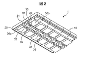
- FIG. 2 is a perspective view showing the configuration of the insulating substrate 1 according to Embodiment 1 of the present invention.
- the heat dissipation layer 10 is formed on one surface of the insulating layer 20, and the wiring layers 30a and 30b are formed on the other surface.
- the insulating layer 20 has a role of electrically insulating between the heat dissipation layer 10 and the wiring layers 30a and 30b.
- a part of the wiring layers 30 a and 30 b is formed as a control signal input circuit 31.
- the control signal input circuit 31 includes a wiring 32 and a connection terminal 35.
- the connection terminal 35 is a terminal for connecting the wiring 32 and the semiconductor element 40 (see FIG. 4).
- the insulating layer 20 can be formed using a ceramic material such as Al 2 O 3 , AlN, or Si 3 N 4 .
- FIG. 3 is a perspective view showing the internal structure of the control signal input circuit 31.
- a part of the wiring 32 is formed as a resistance layer 36.
- the resistance value of the resistance layer 36 is adjusted so that the resistance value (input resistance to the gate electrode) between the circuit that outputs the control signal to the control signal input circuit 31 and the gate electrode of each semiconductor element 40 becomes substantially the same. By doing so, the switching speed of each semiconductor element 40 can be made uniform.
- a terminal that connects the gate electrode in the semiconductor element 40 to the outside of the element is a gate terminal 42. Since the resistance value between the gate electrode and the gate terminal 42 is sufficiently small, it can be ignored.
- a paste containing glass powder is disposed on the insulating layer 20, and then a metal paste (for example, Cu or Ag and glass powder is added) for forming the wiring 32 thereon.
- the metal oxide paste for forming the resistance layer 36 (for example, a paste containing RuO 2 and glass powder) is printed and molded. Thereafter, the insulating layer 20 / glass powder paste / metal paste / metal oxide paste are collectively fired. Thereby, the insulating layer 20 and the control signal input circuit 31 can be formed integrally.
- the glass powder / metal (wiring 32) / metal oxide (resistance layer 36) forming the control signal input circuit 31 are also integrally formed.
- the resistance layer 36 is formed integrally with the wiring 32 as a part of the wiring 32, so that it is not necessary to provide a resistor as a separate chip component.
- the control signal input circuit 31 is formed once without covering the resistance layer 36 as shown in FIG. Thereafter, the resistance value can be finely adjusted by adjusting the length and width of the resistance layer 36 by, for example, laser processing.
- the wiring 32 and the resistance layer 36 are covered, the wiring 32 and the resistance layer 36 can be covered as shown in FIG. 2 by arranging a glass powder paste after fine adjustment and firing the whole again.
- a material that can be laminated and fired on a ceramic material substrate for forming the insulating layer 20 is desirable.
- a material for the glass powder a material that can be laminated and fired on a ceramic material substrate for forming the insulating layer 20 is desirable.
- b) glass powder containing SiO 2 , B 2 O 3 , Al 2 O 3 , alkaline earth metal oxide C) SiO 2 , B 2 O 3 , glass powder containing alkaline earth metal oxide,
- d) SiO 2 , B 2 O 3 , ZrO 2 glass powder containing alkali metal oxide
- One containing silicon oxide such as glass powder containing SiO 2 , alkali metal oxide, or alkaline earth metal oxide, is conceivable.
- FIG. 4 is an internal view showing a state where the semiconductor element 40 is mounted on the insulating substrate 1.
- a state in which some of the components are removed so that the internal structure can be seen is illustrated.
- a mounting state in which the member of reference numeral 31 is absent and the semiconductor element 40 is present is illustrated.
- the wiring 32 is connected to the gate terminal 42 via the connection terminal 35.
- a layer formed by sintering glass powder is formed around the wiring 32, whereby the control signal input circuit 31 is formed as a layer constituting a part of the wiring layers 30a and 30b.
- the glass portion around the wiring 32 also serves to insulate the wiring 32 from the wiring layers (30a, 30b) on both sides thereof.
- the terminal 41 is electrically connected to the wiring layers 30a and 30b and outputs power through the wiring layers 30a and 30b.
- the wiring 32 is formed so as to overlap two adjacent semiconductor elements 40 in the stacking direction of the insulating substrate 1. That is, the wiring 32 is disposed so as to straddle the opposite sides of the two adjacent semiconductor elements 40. Accordingly, compared with the structure in which the control signal input circuit 31 is disposed between the two semiconductor elements 40 as described in FIG. 1, the two semiconductor elements in FIG. 4 are disposed at positions closer to each other. It will be. Therefore, since the length of the wiring 32 can be made shorter than that in FIG. 1, the overall size of the insulating substrate 1 can be reduced, and the electrical resistance due to the wiring 32 can be suppressed.
- A Solder using Sn, Ag, Cu, In, Sb, Pb or the like as a bonding agent for connecting between the gate terminal 42 and the connection terminal 35 and between the terminal 41 and the wiring layers 30a and 30b.
- B Joining material using nano-sized particles such as Ag, Cu, Au, Ni, etc.
- c Submicron-sized Ag particles, Cu particles, and oxides of Ni particles can be used.
- the control signal circuit layer can also be formed of a material containing ceramic powder.
- alumina powder is used instead of glass powder.
- the resistance value of the resistance layer 36 is set so that the resistance value between the circuit that outputs the control signal to the control signal input circuit 31 and the gate electrode of each semiconductor element 40 is substantially the same. It is adjusted.
- the resistance layer 36 is integrally formed with the signal propagation path as a part of the wiring 32.
- the specific resistance value of the resistance layer 36 formed of the metal oxide is generally sufficiently large, and the resistance value necessary for adjusting the switching speed of the semiconductor element 40 can be realized in a small size, so that the size of the insulating substrate 1 can be increased. Can be suppressed.
- the resistance value of the resistance layer 36 can be set to a desired value without unnecessarily increasing the wiring inductance and reducing the control accuracy.
- FIG. 5 is a schematic perspective view showing a part of the insulating substrate 1 according to Embodiment 2 of the present invention.
- a coil 37 for measuring a current passing through the wiring layer 30b is formed inside the wiring layer 30b.
- the coil 37 is formed as a wiring that surrounds the terminal 41 while ensuring insulation.
- the coil 37 can be formed by a method similar to the method for forming the control signal input circuit 31.
- the coil 37 is connected to the control signal input circuit 31, and the current flowing through the terminal 41 can be measured by acquiring the current flowing through the coil 37 via the control signal input circuit 31. Since the coil 37 is disposed in the vicinity of the terminal 41 to be measured, the measurement accuracy is improved and the control accuracy of the semiconductor element 40 is improved as compared with the case where the current is acquired from the terminal 41 via a lead wire or the like. Can be increased.
- FIG. 6 is a perspective view showing a mounting example of the coil 37.
- the coil 37 is not necessarily provided for each semiconductor element 40, and can be provided for only some of the semiconductor elements 40.
- FIG. 6 the example which provided the coil 37 in the two semiconductor elements 40 located diagonally was shown. By separating the interval between the coils 37, the interaction between the coils 37 can be suppressed and the measurement accuracy can be maintained.
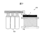
- FIG. 7 is a diagram illustrating a configuration of a unit cell portion of the power conversion device 100 according to the third embodiment of the present invention.
- the power conversion device 100 is a device such as an inverter, a converter, or a power conditioner, for example.
- the power conversion apparatus 100 includes the insulating substrate 1, the heat radiation fin 110, and the smoothing capacitor 120 illustrated in FIG.
- the semiconductor element 40 mounted on the insulating substrate 1 in FIG. 4 is an element that converts DC power into AC power by, for example, a switching element. By using the insulating substrate 1 according to the first and second embodiments, the conversion efficiency of the power conversion device 100 can be improved.
- RuO 2 is exemplified as the metal oxide for forming the resistance layer 36, but other metal oxides can also be used.
- IrO 2 , RhO 2 or the like can be used.
- a mixture of Ag / Pd can be used, and in addition to these, gold, platinum, palladium, silver, copper, or the like can be mixed and used.
- additives such as CuO, V 2 O 5 , MnO 2 , TiO 2 , (c) glass,
- the mixed paste is printed and molded as a part of the control signal input circuit 31 and sintered together with the insulating layer 20.
- the material of the insulating layer 20 for example, silicon nitride ceramics can be used.
- a material of the control signal input circuit 31 for example, a low thermal expansion ceramic having a thermal expansion coefficient close to that of the insulating layer 20 and a material that can be bonded to the insulating layer 20 can be used. Since the thermal expansion coefficient ⁇ of the silicon nitride ceramic substrate is about 3 (ppm / K), for example, a material having a thermal expansion coefficient ⁇ of about 10 (ppm / K) or less is used as the material of the control signal input circuit 31. Good.
- laser processing has been described as a method of adjusting the resistance value of the resistance layer 36, but it can also be adjusted by other methods.
- changing the composition of the material can be mentioned.
- the resistance value of the resistance layer 36 can be adjusted by changing the composition and composition ratio of the materials. Further, it may be possible to realize a desired resistance value by adjusting the dimensions and resistivity of the resistance layer 36 in advance.
- the example in which the semiconductor element 40 is mounted on the insulating substrate 1 has been shown.
- the same configuration as the present invention is adopted. By doing so, it is possible to improve the operation accuracy by aligning the gate resistance value for each circuit element.
- the power conversion device 100 is illustrated as an example of a device provided with the insulating substrate 1, but the operating efficiency of the semiconductor element 40 is improved by using the insulating substrate 1 according to the present invention in other semiconductor devices. Can be made.
- insulating substrate 10 heat dissipation layer 20: insulating layer 30: wiring layers 30a, 30b: wiring layer 31: control signal input circuit 31a: control signal input circuit 32: wiring 32a: wiring 33: bonding wire 34: resistor 35: Connection terminal 36: Resistance layer 37: Coil 40: Semiconductor element 41: Terminal 42: Gate terminal 100: Power converter 110: Radiation fin 120: Smoothing capacitor
Landscapes
- Engineering & Computer Science (AREA)
- Microelectronics & Electronic Packaging (AREA)
- Power Engineering (AREA)
- Inverter Devices (AREA)
- Semiconductor Integrated Circuits (AREA)
- Structures For Mounting Electric Components On Printed Circuit Boards (AREA)
- Parts Printed On Printed Circuit Boards (AREA)
- Power Conversion In General (AREA)
- Chemical & Material Sciences (AREA)
- Ceramic Engineering (AREA)
- Physics & Mathematics (AREA)
- Condensed Matter Physics & Semiconductors (AREA)
- General Physics & Mathematics (AREA)
Abstract
パワー半導体素子のゲート抵抗値を大きくすることによりスイッチング時間のばらつきを調整することができる一方で、ゲート抵抗による損失が大きくなり、システム全体としての電力効率が低下するという課題がある。そこで、回路素子の電力効率に対する影響を抑制しつつ、回路素子のスイッチング速度を揃えることができる、絶縁基板を提供する。本発明に係る絶縁基板において、配線層の一部は制御信号回路層として形成されており、前記制御信号回路層の一部は回路素子が制御信号を受け取るときの入力抵抗値を増加させる抵抗層として形成されている(図2参照)。
Description
本発明は、絶縁基板に関するものである。
パワー半導体素子として、たとえば、IGBT(Insulated Gate Bipolar Transistor)、パワーMOSFETトランジスタ(Metal Oxide Semiconductor Field Effect Transistor)、MOSGTO(MOS Gate Turn-off Thyristor)などが知られている。これらのパワー半導体素子は、素子を制御するための信号をゲート部に対して入力して素子をオン/オフすることにより、電力を制御する。
パワー半導体素子のゲート部は、絶縁基板上に形成された配線と接続され、配線を介してゲート部に対して制御信号を入力する。複数のパワー半導体素子が配線に対して並列接続されている場合、各パワー半導体素子は同時にオン/オフすることが想定されているのが通常である。しかし各パワー半導体素子のスイッチング速度が同一でない場合、先にオン状態となった半導体素子や、オフ状態へ切り替わるのが遅い半導体素子に対して電流が集中し、素子寿命低下や素子破壊が生じる可能性が高まる。
ゲート抵抗値を大きくすると半導体素子のスイッチング時間は長くなり、小さくするとスイッチング時間が短くなる。そこで、ゲート抵抗値を大きくすることにより、スイッチング速度を遅くし、オン/オフ時間のずれが小さくなるように調整することができる。さらに半導体素子内部のゲート抵抗値バラツキなどに起因して各半導体素子のスイッチング時間が大きくばらつかないように、半導体素子内のゲート抵抗の他に、チップ部品として構成されたゲート抵抗部品を、配線とゲート端子との間に設ける場合もある。
下記特許文献1は、ゲート抵抗値を調整する技術について記載している。同文献においては、ゲート電極に接続される端子の一部を固有抵抗の大きい材料によって形成し、この部分の断面積や長さを調節することにより、ゲート抵抗値を調整している。下記特許文献2は、ガラス粉末ペーストと金属ペーストを焼成した基板として、焼結基板上に積層構造を形成する構成例を記載している。
特許文献1記載の技術においては、パワー半導体素子のゲート抵抗値を大きくすることによりスイッチング時間のばらつきを調整することができる一方で、ゲート抵抗による損失が大きくなり、システム全体としての電力効率が低下するという課題がある。
本発明は、上記のような課題に鑑みてなされたものであり、回路素子(例えばパワー半導体素子)の電力効率に対する影響を抑制しつつ、回路素子のスイッチング速度を揃えることができる、絶縁基板を提供することを目的とする。
本発明に係る絶縁基板において、配線層の一部は制御信号回路層として形成されており、前記制御信号回路層の一部は回路素子が制御信号を受け取るときの入力抵抗値を増加させる抵抗層として形成されている。
本開示の絶縁基板は、
放熱層、
第1および第2回路素子と接続する配線が形成された配線層、
前記配線層と前記放熱層との間を電気的に絶縁する絶縁層、
を備え、
前記配線層の一部は、前記第1および第2回路素子に対する制御信号を伝搬する制御信号回路層として形成されており、
前記制御信号回路層の一部は、前記第1および第2回路素子が前記制御信号を受け取るときの入力抵抗値を増加させる抵抗層として形成されている。
放熱層、
第1および第2回路素子と接続する配線が形成された配線層、
前記配線層と前記放熱層との間を電気的に絶縁する絶縁層、
を備え、
前記配線層の一部は、前記第1および第2回路素子に対する制御信号を伝搬する制御信号回路層として形成されており、
前記制御信号回路層の一部は、前記第1および第2回路素子が前記制御信号を受け取るときの入力抵抗値を増加させる抵抗層として形成されている。
前記抵抗層は、前記制御信号回路層の信号伝搬経路を形成する信号配線の一部として、前記信号配線と一体になって形成されていてもよい。
前記制御信号回路層は、ケイ素酸化物を含む材料によって形成されており、
前記抵抗層は、金属酸化物を含む材料によって形成されていてもよい。
前記抵抗層は、金属酸化物を含む材料によって形成されていてもよい。
前記制御信号回路層は、セラミックスを含む材料によって形成されており、
前記抵抗層は、金属酸化物を含む材料によって形成されていてもよい。
前記抵抗層は、金属酸化物を含む材料によって形成されていてもよい。
前記第1回路素子の入力抵抗値と前記第2回路素子の入力抵抗値との間の差は、前記制御信号回路層の信号伝搬経路を形成する信号配線のうち前記抵抗層を除く部分同士の抵抗値の差にくらべて小さいこととしてもよい。
前記抵抗層は、前記第1回路素子の前記入力抵抗値と前記第2回路素子の前記入力抵抗値が同一となる抵抗値を有してもよい。
前記第1回路素子と前記第2回路素子の少なくともいずれかは、電力を出力する電力端子を備え、
前記配線層の一部には、前記電力端子の周囲を取り囲むように配置されたコイルが形成されていてもよい。
前記配線層の一部には、前記電力端子の周囲を取り囲むように配置されたコイルが形成されていてもよい。
前記制御信号回路層の内部には、前記制御信号を伝搬する信号配線が形成されており、 前記信号配線は、前記放熱層、前記絶縁層、および前記配線層の積層方向に沿って前記第1および第2回路素子と重なる位置に形成されていてもよい。
前記第1および第2回路素子は、前記制御信号回路層に対して電気的に互いに並列に接続されていてもよい。
前記絶縁層は、セラミックス材料を用いて形成されていてもよい。
本開示の半導体装置は、
前記絶縁基板上に配置された前記第1および第2回路素子、
を備え、
前記第1および第2回路素子は、半導体素子として構成されている。
前記絶縁基板上に配置された前記第1および第2回路素子、
を備え、
前記第1および第2回路素子は、半導体素子として構成されている。
本発明に係る絶縁基板によれば、ゲート抵抗値の増加による電力効率低下を抑制しつつ、回路素子のスイッチング速度を揃えることができる。
<従来の絶縁基板について>
以下では本発明の理解を容易にするため、まず従来の絶縁基板の構成とその課題について説明する。その後、本発明に係る絶縁基板の構成について説明する。
以下では本発明の理解を容易にするため、まず従来の絶縁基板の構成とその課題について説明する。その後、本発明に係る絶縁基板の構成について説明する。
図1は、従来の絶縁基板の構成を示す斜視図である。絶縁基板は、半導体素子40を搭載する絶縁基板である。半導体素子40は、例えば電力を変換する半導体素子であり、ゲート端子42を介して制御信号を入力することにより制御することができる。端子41は、電力を出力する端子である。
絶縁基板は、放熱層10、絶縁層20、配線層30を備える。配線層30上には、制御信号入力回路31aが形成されている。制御信号入力回路31aは配線32aを備え、配線32aとボンディングワイヤ33を介してゲート端子42に対して制御信号が入力される。各半導体素子40は、制御信号入力回路31aに対して互いに並列に接続されている。
制御信号入力回路31aはさらに、各半導体素子40のスイッチング速度を揃えるため、配線32a上に抵抗器34を備えている場合もある。抵抗器34は、例えばチップ状の独立した電気部品である。
抵抗器34が、完成品として提供されるチップ部品である場合、各抵抗器34の抵抗値を個別に微調整することは困難である。そこで各半導体素子40のスイッチング速度の差を無視できる程度に抑制するため、抵抗器34として抵抗値が比較的大きいものが選択される場合がある。抵抗値が大きければスイッチング速度が遅くなり、個々のスイッチング速度の差が相対的に無視できる範囲内に収まるからである。
しかしこの場合、各半導体素子40全体からなるシステムの電力効率が低下する課題がある。またチップ部品を設けるためにはそのための実装面積が必要であり、絶縁基板1全体のサイズを制約するとともに、その実装面積を確保することによって配線32aが長くなり、さらに抵抗値が増してしまう。
チップ状の抵抗器34を用いることに代えて、例えば特許文献1記載のように、ゲート端子の一部を固有抵抗の大きい材料によって形成し、その材料部分の長さや幅を変化させることにより、抵抗値を調整することも考えられる。この場合、抵抗値を大きくするためには、抵抗部分を長くするかあるいは幅を狭くする必要がある。しかしゲート端子長そのものを長くすると絶縁基板全体としてのサイズが大きくなってしまうので、例えば端子を折り曲げて螺旋状にし、ゲート端子長を抑制する必要がある。また、ゲート端子幅そのものを狭くすると端子としての剛性が低下し、熱負荷によりゲート端子や接続部の信頼性が低下する可能性があるので、ゲート端子幅を狭くすることは望ましくない。さらに、半導体素子40のスイッチングを高精度に制御するためには、スイッチング周波数を上げる必要があるが、端子長増加や端子幅縮小は配線のインダクタンス上昇につながり、高い周波数で半導体素子40を精度よく制御することが困難になる。
そこで本発明においては、スイッチング速度を調整するための抵抗を配線と一体的に形成することにより、半導体素子外部に設ける抵抗部の実装面積を抑制することを図る。さらに抵抗層を配線の一部として形成することにより、抵抗層を形成した後に加工を施して抵抗値を微調整できるようにする。
<実施の形態1>
図2は、本発明の実施形態1に係る絶縁基板1の構成を示す斜視図である。絶縁層20の片面には放熱層10が形成され、他面には配線層30a,30bが形成されている。絶縁層20は放熱層10と配線層30a,30bとの間を電気的に絶縁する役割を有する。配線層30a,30bの一部は、制御信号入力回路31として形成されている。制御信号入力回路31は、配線32と接続端子35を有する。接続端子35は、配線32と半導体素子40(図4を参照)を接続するための端子である。絶縁層20は、例えばAl2O3、AlN或いはSi3N4などのセラミックス材料を用いて形成することができる。
図2は、本発明の実施形態1に係る絶縁基板1の構成を示す斜視図である。絶縁層20の片面には放熱層10が形成され、他面には配線層30a,30bが形成されている。絶縁層20は放熱層10と配線層30a,30bとの間を電気的に絶縁する役割を有する。配線層30a,30bの一部は、制御信号入力回路31として形成されている。制御信号入力回路31は、配線32と接続端子35を有する。接続端子35は、配線32と半導体素子40(図4を参照)を接続するための端子である。絶縁層20は、例えばAl2O3、AlN或いはSi3N4などのセラミックス材料を用いて形成することができる。
図3は、制御信号入力回路31の内部構造を示す斜視図である。配線32の一部は、抵抗層36として形成されている。制御信号入力回路31に対して制御信号を出力する回路と各半導体素子40のゲート電極との間の抵抗値(ゲート電極に対する入力抵抗)が略同一となるように抵抗層36の抵抗値を調整することにより、各半導体素子40のスイッチング速度を揃えることができる。半導体素子40内のゲート電極を素子外部に接続する端子がゲート端子42である。ゲート電極とゲート端子42間の抵抗値は十分に小さいので無視して差し支えない。
制御信号入力回路31を形成する際には、まず絶縁層20上にガラス粉末を配合したペーストを配置し、その上に配線32を形成するための金属ペースト(例えばCuやAgとガラス粉末を配合したペースト)を印刷成型し、さらに抵抗層36を形成するための金属酸化物ペースト(例えばRuO2とガラス粉末を配合したペースト)を印刷成型する。その後、絶縁層20/ガラス粉末ペースト/金属ペースト/金属酸化物ペーストをまとめて焼成する。これにより、絶縁層20と制御信号入力回路31を一体的に形成することができる。
絶縁層20と制御信号入力回路31を焼成する過程において、制御信号入力回路31を形成するガラス粉末/金属(配線32)/金属酸化物(抵抗層36)も一体的に形成される。これにより、抵抗層36は配線32の一部として配線32と一体になって形成されるので、別途チップ部品として抵抗器を設ける必要はない。
抵抗層36の抵抗値を微調整する場合、まず図3に示すように抵抗層36を被覆しない状態で制御信号入力回路31をいったん形成する。その後、例えばレーザ加工などにより抵抗層36の長さや幅を調整することにより、抵抗値を微調整することができる。配線32や抵抗層36をカバーする場合は、微調整後にさらにガラス粉末ペーストを配して改めて全体を焼成することにより、図2に示すように配線32や抵抗層36を被覆することができる。
ガラス粉末の材料としては、絶縁層20を形成するセラミックス材料の基板に積層して焼成することができるものが望ましい。例えば、(a)SiO2、B2O3、アルカリ金属酸化物を含有するガラス粉末、(b)SiO2、B2O3、Al2O3、アルカリ土類金属酸化物を含有するガラス粉末、(c)SiO2、B2O3、アルカリ土類金属酸化物を含有するガラス粉末、(d)SiO2、B2O3、ZrO2、アルカリ金属酸化物を含有するガラス粉末、(e)SiO2、アルカリ金属酸化物、アルカリ土類金属酸化物を含有するガラス粉末、などのように、ケイ素酸化物を含有するものが考えられる。
図4は、絶縁基板1に半導体素子40を実装した状態を示す内部図である。説明の便宜上、内部の構造が見えるように構成要素の一部を取り除いた状態を図示する。ここでは図2~図3で説明した放熱層10/絶縁層20/配線層30a,30bの積層構造(符号31の部材有り)と、放熱層10/絶縁層20/配線層30の積層構造(符号31の部材無し。半導体素子40有り)とを重ね合わせた実装状態を例示する。
配線32は、接続端子35を介してゲート端子42と接続されている。配線32の周りは、ガラス粉末を焼結することにより形成された層が形成され、これにより制御信号入力回路31は配線層30a,30bの一部を構成する層として形成されている。配線32の周りのガラス部分は、配線32をその両側の配線層(30a,30b)から絶縁する役割も有する。端子41は、配線層30a,30bと電気的に接続され、配線層30a,30bを介して電力を出力する。
配線32は、絶縁基板1の積層方向において、隣接する2つの半導体素子40と重なるように形成されている。すなわち配線32は、隣接する2つの半導体素子40の対向辺にまたがるように配置されている。これにより、図1で説明したような2つの半導体素子40の間に制御信号入力回路31が配置されている構造と比較すると、図4における2つの半導体素子は互いにより接近した位置に配置されることになる。したがって、図1と比較して配線32の長さをより短くすることができるので、絶縁基板1全体のサイズを小さくできるとともに、配線32による電気抵抗を抑制することができる。
ゲート端子42と接続端子35との間、および端子41と配線層30a,30bとの間を接続する接合剤としては、(a)Sn、Ag、Cu、In、Sb、Pbなどを用いたはんだ、(b)Ag、Cu、Au、Niなどのナノサイズ粒子を用いた接合材、(c)サブミクロンサイズのAg粒子やCu粒子およびNi粒子の酸化物、などを用いることができる。
セラミックス粉末を含む材料で制御信号回路層を形成することもできる。例えば、実施形態1の構成について、ガラス粉末に代えてアルミナ粉末を用いる。但し、実施形態1のようにガラス粉末ペーストと金属ペーストを用いる方が、効率よく同時焼成を進めて安定して制御信号回路層を形成できるのでより好ましい。
制御信号回路層の信号伝搬経路を形成する信号配線(但し、抵抗層を除く)同士の抵抗値の差にくらべて、回路素子の入力抵抗同士の差が小さいほどよい。例えば1つ目の半導体素子40の入力抵抗値と2つ目の半導体素子40の入力抵抗値との間の差分は、1つ目の半導体素子40に接続された信号配線の抵抗値と2つ目の半導体素子40に接続された信号配線の抵抗値との間の差分よりも小さいほどよい。したがって、実施形態1では、制御信号入力回路31に対して制御信号を出力する回路と各半導体素子40のゲート電極との間の抵抗値が略同一となるように、抵抗層36の抵抗値を調整している。
<実施の形態1:まとめ>
本実施形態1に係る絶縁基板1において、抵抗層36は、配線32の一部として信号伝搬経路と一体になって形成されている。金属酸化物によって形成された抵抗層36の固有抵抗値は一般に充分に大きく、半導体素子40のスイッチング速度を調整するために必要な抵抗値を小さなサイズで実現できるので、絶縁基板1のサイズ増加を抑制することができる。
本実施形態1に係る絶縁基板1において、抵抗層36は、配線32の一部として信号伝搬経路と一体になって形成されている。金属酸化物によって形成された抵抗層36の固有抵抗値は一般に充分に大きく、半導体素子40のスイッチング速度を調整するために必要な抵抗値を小さなサイズで実現できるので、絶縁基板1のサイズ増加を抑制することができる。
本実施形態1に係る絶縁基板1において、抵抗層36の抵抗値を高くするために配線長を増やしたり配線幅を狭くしたりする必要はない。したがって、配線のインダクタンスを不必要に高くして制御精度を低下させることなく、抵抗層36の抵抗値を所望値にすることができる。
<実施の形態2>
図5は、本発明の実施形態2に係る絶縁基板1の一部を示す概略斜視図である。本実施形態2においては、配線層30bの内部に、配線層30bを通過する電流を計測するためのコイル37が形成されている。コイル37は、絶縁を確保しつつ端子41の周りを取り囲む配線として形成されている。コイル37は、制御信号入力回路31を形成する方法と同様の方法により形成することができる。
図5は、本発明の実施形態2に係る絶縁基板1の一部を示す概略斜視図である。本実施形態2においては、配線層30bの内部に、配線層30bを通過する電流を計測するためのコイル37が形成されている。コイル37は、絶縁を確保しつつ端子41の周りを取り囲む配線として形成されている。コイル37は、制御信号入力回路31を形成する方法と同様の方法により形成することができる。
端子41に電流が流れると、コイル37にも電流が誘導される。コイル37は制御信号入力回路31に接続されており、制御信号入力回路31を介してコイル37に流れる電流を取得することにより、端子41に流れる電流を計測することができる。コイル37は計測対象である端子41の近傍に配置されているので、引き出し線などを介して端子41から電流を取得する場合と比較して、計測精度を向上させ、半導体素子40の制御精度をより高めることができる。
図6は、コイル37の実装例を示す斜視図である。コイル37は、必ずしも半導体素子40ごとに設ける必要はなく、いずれか一部の半導体素子40についてのみ設けることもできる。図6においては、対角上に位置する2つの半導体素子40にコイル37を設けた例を示した。コイル37間の間隔を離すことにより、コイル37間の相互作用を抑制し、計測精度を保つことができる。
<実施の形態3>
図7は、本発明の実施形態3に係る電力変換装置100のユニットセル部分の構成を表す図である。電力変換装置100は、例えばインバータ、コンバータ、パワーコンディショナなどの装置である。電力変換装置100は、実施形態1~2いずれかで説明した図4の絶縁基板1、放熱フィン110、平滑コンデンサ120を備えている。図4の絶縁基板1が実装している半導体素子40は、例えばスイッチング素子によって直流電力を交流電力に変換する素子である。実施形態1~2に係る絶縁基板1を用いることにより、電力変換装置100の変換効率を向上させることができる。
図7は、本発明の実施形態3に係る電力変換装置100のユニットセル部分の構成を表す図である。電力変換装置100は、例えばインバータ、コンバータ、パワーコンディショナなどの装置である。電力変換装置100は、実施形態1~2いずれかで説明した図4の絶縁基板1、放熱フィン110、平滑コンデンサ120を備えている。図4の絶縁基板1が実装している半導体素子40は、例えばスイッチング素子によって直流電力を交流電力に変換する素子である。実施形態1~2に係る絶縁基板1を用いることにより、電力変換装置100の変換効率を向上させることができる。
<本発明の変形例について>
本発明は上記実施形態に限定されるものではなく、様々な変形例が含まれる。例えば、上記した実施形態は本発明を分かりやすく説明するために詳細に説明したものであり、必ずしも説明した全ての構成を備えるものに限定されるものではない。
本発明は上記実施形態に限定されるものではなく、様々な変形例が含まれる。例えば、上記した実施形態は本発明を分かりやすく説明するために詳細に説明したものであり、必ずしも説明した全ての構成を備えるものに限定されるものではない。
以上の実施形態において、抵抗層36を形成するための金属酸化物としてRuO2を例示したが、その他金属酸化物を用いることもできる。例えばIrO2、RhO2などを用いることができる。さらには、Ag/Pdの混合物を用いることもできるし、これらに加えて金、白金、パラジウム、銀、銅などを混合して用いることもできる。抵抗層36を形成する際には、例えば(a)これら金属酸化物または金属の粉体、(b)CuO、V2O5、MnO2、TiO2などの添加物、(c)ガラス、を混合したペーストを制御信号入力回路31の一部として印刷成型し、絶縁層20とともに焼結する。
以上の実施形態において、絶縁層20の材料としては、例えば窒化珪素セラミックスを用いることができる。制御信号入力回路31の材料としては、例えば絶縁層20と熱膨張係数が近い低熱膨張性セラミックスであって、絶縁層20に接合することができる材料を用いることができる。窒化珪素セラミックス基板の熱膨張係数αは3(ppm/K)程度であるので、制御信号入力回路31の材料としては、例えば熱膨張係数αが10(ppm/K)以下程度のものを用いればよい。
以上の実施形態において、抵抗層36の抵抗値を調整する方法としてレーザ加工することを説明したが、その他方法により調整することもできる。例えば材料の配合を変更することが挙げられる。例えば抵抗層36の材料として、(a)RuO2のみを用いる、(b)ケイ素酸化物とRuO2の混合物を用いる、(c)上記(a)(b)に対して銀を加える、などが考えられる。材料の配合や組成比を変えることにより、抵抗層36の抵抗値を調整することができる。さらには、抵抗層36の寸法や抵抗率をあらかじめ調整しておくことにより、所望の抵抗値を実現することも考えられる。
以上の実施形態において、絶縁基板1上に半導体素子40を実装した例を示したが、半導体素子40以外の回路素子を絶縁基板1上に実装する場合においても、本発明と同様の構成を採用することにより、各回路素子に対するゲート抵抗値を揃えて動作精度を向上させることができる。
以上の実施形態において、絶縁基板1を備えた装置の例として電力変換装置100を例示したが、その他半導体装置においても本発明に係る絶縁基板1を用いることにより、半導体素子40の動作効率を向上させることができる。
1:絶縁基板
10:放熱層
20:絶縁層
30:配線層
30a、30b:配線層
31:制御信号入力回路
31a:制御信号入力回路
32:配線
32a:配線
33:ボンディングワイヤ
34:抵抗器
35:接続端子
36:抵抗層
37:コイル
40:半導体素子
41:端子
42:ゲート端子
100:電力変換装置
110:放熱フィン
120:平滑コンデンサ
10:放熱層
20:絶縁層
30:配線層
30a、30b:配線層
31:制御信号入力回路
31a:制御信号入力回路
32:配線
32a:配線
33:ボンディングワイヤ
34:抵抗器
35:接続端子
36:抵抗層
37:コイル
40:半導体素子
41:端子
42:ゲート端子
100:電力変換装置
110:放熱フィン
120:平滑コンデンサ
Claims (11)
- 放熱層、
第1および第2回路素子と接続する配線が形成された配線層、
前記配線層と前記放熱層との間を電気的に絶縁する絶縁層、
を備え、
前記配線層の一部は、前記第1および第2回路素子に対する制御信号を伝搬する制御信号回路層として形成されており、
前記制御信号回路層の一部は、前記第1および第2回路素子が前記制御信号を受け取るときの入力抵抗値を増加させる抵抗層として形成されている
ことを特徴とする絶縁基板。 - 前記抵抗層は、前記制御信号回路層の信号伝搬経路を形成する信号配線の一部として、前記信号配線と一体になって形成されている
ことを特徴とする請求項1記載の絶縁基板。 - 前記制御信号回路層は、ケイ素酸化物を含む材料によって形成されており、
前記抵抗層は、金属酸化物を含む材料によって形成されている
ことを特徴とする請求項1記載の絶縁基板。 - 前記制御信号回路層は、セラミックスを含む材料によって形成されており、
前記抵抗層は、金属酸化物を含む材料によって形成されている
ことを特徴とする請求項1記載の絶縁基板。 - 前記第1回路素子の入力抵抗値と前記第2回路素子の入力抵抗値との間の差は、前記制御信号回路層の信号伝搬経路を形成する信号配線のうち前記抵抗層を除く部分同士の抵抗値の差にくらべて小さい
ことを特徴とする請求項1記載の絶縁基板。 - 前記抵抗層は、前記第1回路素子の前記入力抵抗値と前記第2回路素子の前記入力抵抗値が同一となる抵抗値を有する
ことを特徴とする請求項1記載の絶縁基板。 - 前記第1回路素子と前記第2回路素子の少なくともいずれかは、電力を出力する電力端子を備え、
前記配線層の一部には、前記電力端子の周囲を取り囲むように配置されたコイルが形成されている
ことを特徴とする請求項1記載の絶縁基板。 - 前記制御信号回路層の内部には、前記制御信号を伝搬する信号配線が形成されており、 前記信号配線は、前記放熱層、前記絶縁層、および前記配線層の積層方向に沿って前記第1および第2回路素子と重なる位置に形成されている
ことを特徴とする請求項1記載の絶縁基板。 - 前記第1および第2回路素子は、前記制御信号回路層に対して電気的に互いに並列に接続されている
ことを特徴とする請求項1記載の絶縁基板。 - 前記絶縁層は、セラミックス材料を用いて形成されている
ことを特徴とする請求項1記載の絶縁基板。 - 請求項1から10のいずれか1項記載の絶縁基板、
前記絶縁基板上に配置された前記第1および第2回路素子、
を備え、
前記第1および第2回路素子は、半導体素子として構成されている
ことを特徴とする半導体装置。
Priority Applications (3)
| Application Number | Priority Date | Filing Date | Title |
|---|---|---|---|
| JP2018537089A JP6721051B2 (ja) | 2016-09-01 | 2017-08-09 | 絶縁基板およびこれを用いた半導体装置 |
| DE112017001953.2T DE112017001953B4 (de) | 2016-09-01 | 2017-08-09 | Isolierendes Substrat und Halbleitervorrichtung, die dieses verwendet |
| US16/099,457 US10559509B2 (en) | 2016-09-01 | 2017-08-09 | Insulating substrate and semiconductor device using same |
Applications Claiming Priority (2)
| Application Number | Priority Date | Filing Date | Title |
|---|---|---|---|
| JP2016171196 | 2016-09-01 | ||
| JP2016-171196 | 2016-09-01 |
Publications (1)
| Publication Number | Publication Date |
|---|---|
| WO2018043076A1 true WO2018043076A1 (ja) | 2018-03-08 |
Family
ID=61300527
Family Applications (1)
| Application Number | Title | Priority Date | Filing Date |
|---|---|---|---|
| PCT/JP2017/028889 Ceased WO2018043076A1 (ja) | 2016-09-01 | 2017-08-09 | 絶縁基板およびこれを用いた半導体装置 |
Country Status (4)
| Country | Link |
|---|---|
| US (1) | US10559509B2 (ja) |
| JP (1) | JP6721051B2 (ja) |
| DE (1) | DE112017001953B4 (ja) |
| WO (1) | WO2018043076A1 (ja) |
Cited By (2)
| Publication number | Priority date | Publication date | Assignee | Title |
|---|---|---|---|---|
| JP2019197763A (ja) * | 2018-05-08 | 2019-11-14 | 三菱電機株式会社 | 半導体パワーモジュール |
| WO2025196919A1 (ja) * | 2024-03-18 | 2025-09-25 | 三菱電機株式会社 | 電子機器 |
Families Citing this family (1)
| Publication number | Priority date | Publication date | Assignee | Title |
|---|---|---|---|---|
| CN119673883B (zh) * | 2024-12-03 | 2025-10-14 | 珠海格力电子元器件有限公司 | 智能功率模块 |
Citations (5)
| Publication number | Priority date | Publication date | Assignee | Title |
|---|---|---|---|---|
| JPH0472650U (ja) * | 1990-11-06 | 1992-06-26 | ||
| JPH11317495A (ja) * | 1998-05-06 | 1999-11-16 | Mitsubishi Electric Corp | 絶縁ゲート型バイポーラトランジスタモジュールおよび駆動回路付絶縁ゲート型バイポーラトランジスタモジュール |
| JP2000171491A (ja) * | 1998-12-03 | 2000-06-23 | Mitsubishi Electric Corp | パワー半導体モジュール |
| JP2007317904A (ja) * | 2006-05-26 | 2007-12-06 | Toppan Printing Co Ltd | 抵抗素子及び抵抗素子内蔵配線回路板 |
| JP2012084621A (ja) * | 2010-10-08 | 2012-04-26 | Meidensha Corp | 電極端子及び半導体モジュール |
Family Cites Families (2)
| Publication number | Priority date | Publication date | Assignee | Title |
|---|---|---|---|---|
| JP3476612B2 (ja) | 1995-12-21 | 2003-12-10 | 三菱電機株式会社 | 半導体装置 |
| JP5463235B2 (ja) | 2010-07-30 | 2014-04-09 | 日立オートモティブシステムズ株式会社 | 車載用電子機器に用いる基板構造 |
-
2017
- 2017-08-09 WO PCT/JP2017/028889 patent/WO2018043076A1/ja not_active Ceased
- 2017-08-09 DE DE112017001953.2T patent/DE112017001953B4/de active Active
- 2017-08-09 JP JP2018537089A patent/JP6721051B2/ja active Active
- 2017-08-09 US US16/099,457 patent/US10559509B2/en active Active
Patent Citations (5)
| Publication number | Priority date | Publication date | Assignee | Title |
|---|---|---|---|---|
| JPH0472650U (ja) * | 1990-11-06 | 1992-06-26 | ||
| JPH11317495A (ja) * | 1998-05-06 | 1999-11-16 | Mitsubishi Electric Corp | 絶縁ゲート型バイポーラトランジスタモジュールおよび駆動回路付絶縁ゲート型バイポーラトランジスタモジュール |
| JP2000171491A (ja) * | 1998-12-03 | 2000-06-23 | Mitsubishi Electric Corp | パワー半導体モジュール |
| JP2007317904A (ja) * | 2006-05-26 | 2007-12-06 | Toppan Printing Co Ltd | 抵抗素子及び抵抗素子内蔵配線回路板 |
| JP2012084621A (ja) * | 2010-10-08 | 2012-04-26 | Meidensha Corp | 電極端子及び半導体モジュール |
Cited By (2)
| Publication number | Priority date | Publication date | Assignee | Title |
|---|---|---|---|---|
| JP2019197763A (ja) * | 2018-05-08 | 2019-11-14 | 三菱電機株式会社 | 半導体パワーモジュール |
| WO2025196919A1 (ja) * | 2024-03-18 | 2025-09-25 | 三菱電機株式会社 | 電子機器 |
Also Published As
| Publication number | Publication date |
|---|---|
| US20190221489A1 (en) | 2019-07-18 |
| JP6721051B2 (ja) | 2020-07-08 |
| DE112017001953T5 (de) | 2018-12-27 |
| US10559509B2 (en) | 2020-02-11 |
| DE112017001953B4 (de) | 2021-08-19 |
| JPWO2018043076A1 (ja) | 2019-06-24 |
Similar Documents
| Publication | Publication Date | Title |
|---|---|---|
| CN102956610B (zh) | 半导体装置 | |
| CN103403862B (zh) | 功率半导体模块和用于制造与温度传感器一起烧结的功率半导体模块的方法 | |
| CN112053994B (zh) | 半导体衬底和半导体装置 | |
| CN110176446B (zh) | 半导体装置 | |
| CN106856669A (zh) | 半导体装置及其制造方法 | |
| US12599006B2 (en) | Electronic device | |
| JP6721051B2 (ja) | 絶縁基板およびこれを用いた半導体装置 | |
| JP6261642B2 (ja) | 電力半導体装置 | |
| WO2012026418A1 (ja) | 半導体装置 | |
| WO2021251126A1 (ja) | 半導体装置 | |
| CN107871733A (zh) | 半导体模块 | |
| JP6585847B2 (ja) | 電動機のための電力モジュール | |
| JP7288043B2 (ja) | プリント基板に表面実装するための抵抗部品、および少なくとも1つの抵抗部品が配置されたプリント基板 | |
| JP2005129826A (ja) | パワー半導体装置 | |
| JP2021182575A (ja) | 半導体装置内部スナバ回路接続構造及びこれを用いたパワーモジュール構造 | |
| CN108933087B (zh) | 功率模块 | |
| CN103681552B (zh) | 功率半导体模块和用于制造功率半导体模块的方法 | |
| JP7557525B2 (ja) | 半導体装置 | |
| JP2012084621A (ja) | 電極端子及び半導体モジュール | |
| CN112309994B (zh) | 半导体模块装置 | |
| JP2016001644A (ja) | 半導体モジュール | |
| CN111584422B (zh) | 半导体装置及其制造方法 | |
| CN112397473B (zh) | 具有集成多抽头阻抗结构的封装体 | |
| JP2020161680A (ja) | パワーモジュール | |
| JP2024133026A (ja) | ノイズフィルタおよび電子機器 |
Legal Events
| Date | Code | Title | Description |
|---|---|---|---|
| 121 | Ep: the epo has been informed by wipo that ep was designated in this application |
Ref document number: 17846085 Country of ref document: EP Kind code of ref document: A1 |
|
| ENP | Entry into the national phase |
Ref document number: 2018537089 Country of ref document: JP Kind code of ref document: A |
|
| 122 | Ep: pct application non-entry in european phase |
Ref document number: 17846085 Country of ref document: EP Kind code of ref document: A1 |