WO2018042711A1 - 液晶表示装置 - Google Patents
液晶表示装置 Download PDFInfo
- Publication number
- WO2018042711A1 WO2018042711A1 PCT/JP2017/007313 JP2017007313W WO2018042711A1 WO 2018042711 A1 WO2018042711 A1 WO 2018042711A1 JP 2017007313 W JP2017007313 W JP 2017007313W WO 2018042711 A1 WO2018042711 A1 WO 2018042711A1
- Authority
- WO
- WIPO (PCT)
- Prior art keywords
- data
- latch
- level
- pixels
- liquid crystal
- Prior art date
- Legal status (The legal status is an assumption and is not a legal conclusion. Google has not performed a legal analysis and makes no representation as to the accuracy of the status listed.)
- Ceased
Links
Images


Classifications
-
- G—PHYSICS
- G09—EDUCATION; CRYPTOGRAPHY; DISPLAY; ADVERTISING; SEALS
- G09G—ARRANGEMENTS OR CIRCUITS FOR CONTROL OF INDICATING DEVICES USING STATIC MEANS TO PRESENT VARIABLE INFORMATION
- G09G3/00—Control arrangements or circuits, of interest only in connection with visual indicators other than cathode-ray tubes
- G09G3/20—Control arrangements or circuits, of interest only in connection with visual indicators other than cathode-ray tubes for presentation of an assembly of a number of characters, e.g. a page, by composing the assembly by combination of individual elements arranged in a matrix no fixed position being assigned to or needed to be assigned to the individual characters or partial characters
- G09G3/2007—Display of intermediate tones
- G09G3/2018—Display of intermediate tones by time modulation using two or more time intervals
- G09G3/2022—Display of intermediate tones by time modulation using two or more time intervals using sub-frames
-
- G—PHYSICS
- G02—OPTICS
- G02F—OPTICAL DEVICES OR ARRANGEMENTS FOR THE CONTROL OF LIGHT BY MODIFICATION OF THE OPTICAL PROPERTIES OF THE MEDIA OF THE ELEMENTS INVOLVED THEREIN; NON-LINEAR OPTICS; FREQUENCY-CHANGING OF LIGHT; OPTICAL LOGIC ELEMENTS; OPTICAL ANALOGUE/DIGITAL CONVERTERS
- G02F1/00—Devices or arrangements for the control of the intensity, colour, phase, polarisation or direction of light arriving from an independent light source, e.g. switching, gating or modulating; Non-linear optics
- G02F1/01—Devices or arrangements for the control of the intensity, colour, phase, polarisation or direction of light arriving from an independent light source, e.g. switching, gating or modulating; Non-linear optics for the control of the intensity, phase, polarisation or colour
- G02F1/13—Devices or arrangements for the control of the intensity, colour, phase, polarisation or direction of light arriving from an independent light source, e.g. switching, gating or modulating; Non-linear optics for the control of the intensity, phase, polarisation or colour based on liquid crystals, e.g. single liquid crystal display cells
- G02F1/133—Constructional arrangements; Operation of liquid crystal cells; Circuit arrangements
- G02F1/1333—Constructional arrangements; Manufacturing methods
- G02F1/1335—Structural association of cells with optical devices, e.g. polarisers or reflectors
- G02F1/133553—Reflecting elements
-
- G—PHYSICS
- G02—OPTICS
- G02F—OPTICAL DEVICES OR ARRANGEMENTS FOR THE CONTROL OF LIGHT BY MODIFICATION OF THE OPTICAL PROPERTIES OF THE MEDIA OF THE ELEMENTS INVOLVED THEREIN; NON-LINEAR OPTICS; FREQUENCY-CHANGING OF LIGHT; OPTICAL LOGIC ELEMENTS; OPTICAL ANALOGUE/DIGITAL CONVERTERS
- G02F1/00—Devices or arrangements for the control of the intensity, colour, phase, polarisation or direction of light arriving from an independent light source, e.g. switching, gating or modulating; Non-linear optics
- G02F1/01—Devices or arrangements for the control of the intensity, colour, phase, polarisation or direction of light arriving from an independent light source, e.g. switching, gating or modulating; Non-linear optics for the control of the intensity, phase, polarisation or colour
- G02F1/13—Devices or arrangements for the control of the intensity, colour, phase, polarisation or direction of light arriving from an independent light source, e.g. switching, gating or modulating; Non-linear optics for the control of the intensity, phase, polarisation or colour based on liquid crystals, e.g. single liquid crystal display cells
- G02F1/133—Constructional arrangements; Operation of liquid crystal cells; Circuit arrangements
- G02F1/1333—Constructional arrangements; Manufacturing methods
- G02F1/1343—Electrodes
- G02F1/13439—Electrodes characterised by their electrical, optical, physical properties; materials therefor; method of making
-
- G—PHYSICS
- G02—OPTICS
- G02F—OPTICAL DEVICES OR ARRANGEMENTS FOR THE CONTROL OF LIGHT BY MODIFICATION OF THE OPTICAL PROPERTIES OF THE MEDIA OF THE ELEMENTS INVOLVED THEREIN; NON-LINEAR OPTICS; FREQUENCY-CHANGING OF LIGHT; OPTICAL LOGIC ELEMENTS; OPTICAL ANALOGUE/DIGITAL CONVERTERS
- G02F1/00—Devices or arrangements for the control of the intensity, colour, phase, polarisation or direction of light arriving from an independent light source, e.g. switching, gating or modulating; Non-linear optics
- G02F1/01—Devices or arrangements for the control of the intensity, colour, phase, polarisation or direction of light arriving from an independent light source, e.g. switching, gating or modulating; Non-linear optics for the control of the intensity, phase, polarisation or colour
- G02F1/13—Devices or arrangements for the control of the intensity, colour, phase, polarisation or direction of light arriving from an independent light source, e.g. switching, gating or modulating; Non-linear optics for the control of the intensity, phase, polarisation or colour based on liquid crystals, e.g. single liquid crystal display cells
- G02F1/133—Constructional arrangements; Operation of liquid crystal cells; Circuit arrangements
- G02F1/136—Liquid crystal cells structurally associated with a semi-conducting layer or substrate, e.g. cells forming part of an integrated circuit
- G02F1/1362—Active matrix addressed cells
- G02F1/136277—Active matrix addressed cells formed on a semiconductor substrate, e.g. of silicon
-
- G—PHYSICS
- G09—EDUCATION; CRYPTOGRAPHY; DISPLAY; ADVERTISING; SEALS
- G09G—ARRANGEMENTS OR CIRCUITS FOR CONTROL OF INDICATING DEVICES USING STATIC MEANS TO PRESENT VARIABLE INFORMATION
- G09G3/00—Control arrangements or circuits, of interest only in connection with visual indicators other than cathode-ray tubes
- G09G3/20—Control arrangements or circuits, of interest only in connection with visual indicators other than cathode-ray tubes for presentation of an assembly of a number of characters, e.g. a page, by composing the assembly by combination of individual elements arranged in a matrix no fixed position being assigned to or needed to be assigned to the individual characters or partial characters
- G09G3/34—Control arrangements or circuits, of interest only in connection with visual indicators other than cathode-ray tubes for presentation of an assembly of a number of characters, e.g. a page, by composing the assembly by combination of individual elements arranged in a matrix no fixed position being assigned to or needed to be assigned to the individual characters or partial characters by control of light from an independent source
- G09G3/36—Control arrangements or circuits, of interest only in connection with visual indicators other than cathode-ray tubes for presentation of an assembly of a number of characters, e.g. a page, by composing the assembly by combination of individual elements arranged in a matrix no fixed position being assigned to or needed to be assigned to the individual characters or partial characters by control of light from an independent source using liquid crystals
- G09G3/3611—Control of matrices with row and column drivers
- G09G3/3685—Details of drivers for data electrodes
- G09G3/3688—Details of drivers for data electrodes suitable for active matrices only
-
- G—PHYSICS
- G02—OPTICS
- G02F—OPTICAL DEVICES OR ARRANGEMENTS FOR THE CONTROL OF LIGHT BY MODIFICATION OF THE OPTICAL PROPERTIES OF THE MEDIA OF THE ELEMENTS INVOLVED THEREIN; NON-LINEAR OPTICS; FREQUENCY-CHANGING OF LIGHT; OPTICAL LOGIC ELEMENTS; OPTICAL ANALOGUE/DIGITAL CONVERTERS
- G02F2203/00—Function characteristic
- G02F2203/02—Function characteristic reflective
-
- G—PHYSICS
- G02—OPTICS
- G02F—OPTICAL DEVICES OR ARRANGEMENTS FOR THE CONTROL OF LIGHT BY MODIFICATION OF THE OPTICAL PROPERTIES OF THE MEDIA OF THE ELEMENTS INVOLVED THEREIN; NON-LINEAR OPTICS; FREQUENCY-CHANGING OF LIGHT; OPTICAL LOGIC ELEMENTS; OPTICAL ANALOGUE/DIGITAL CONVERTERS
- G02F2203/00—Function characteristic
- G02F2203/30—Gray scale
-
- G—PHYSICS
- G09—EDUCATION; CRYPTOGRAPHY; DISPLAY; ADVERTISING; SEALS
- G09G—ARRANGEMENTS OR CIRCUITS FOR CONTROL OF INDICATING DEVICES USING STATIC MEANS TO PRESENT VARIABLE INFORMATION
- G09G2300/00—Aspects of the constitution of display devices
- G09G2300/04—Structural and physical details of display devices
- G09G2300/0439—Pixel structures
-
- G—PHYSICS
- G09—EDUCATION; CRYPTOGRAPHY; DISPLAY; ADVERTISING; SEALS
- G09G—ARRANGEMENTS OR CIRCUITS FOR CONTROL OF INDICATING DEVICES USING STATIC MEANS TO PRESENT VARIABLE INFORMATION
- G09G2300/00—Aspects of the constitution of display devices
- G09G2300/08—Active matrix structure, i.e. with use of active elements, inclusive of non-linear two terminal elements, in the pixels together with light emitting or modulating elements
- G09G2300/0809—Several active elements per pixel in active matrix panels
- G09G2300/0842—Several active elements per pixel in active matrix panels forming a memory circuit, e.g. a dynamic memory with one capacitor
- G09G2300/0857—Static memory circuit, e.g. flip-flop
-
- G—PHYSICS
- G09—EDUCATION; CRYPTOGRAPHY; DISPLAY; ADVERTISING; SEALS
- G09G—ARRANGEMENTS OR CIRCUITS FOR CONTROL OF INDICATING DEVICES USING STATIC MEANS TO PRESENT VARIABLE INFORMATION
- G09G2310/00—Command of the display device
- G09G2310/02—Addressing, scanning or driving the display screen or processing steps related thereto
- G09G2310/0264—Details of driving circuits
- G09G2310/027—Details of drivers for data electrodes, the drivers handling digital grey scale data, e.g. use of D/A converters
-
- G—PHYSICS
- G09—EDUCATION; CRYPTOGRAPHY; DISPLAY; ADVERTISING; SEALS
- G09G—ARRANGEMENTS OR CIRCUITS FOR CONTROL OF INDICATING DEVICES USING STATIC MEANS TO PRESENT VARIABLE INFORMATION
- G09G2310/00—Command of the display device
- G09G2310/08—Details of timing specific for flat panels, other than clock recovery
-
- G—PHYSICS
- G09—EDUCATION; CRYPTOGRAPHY; DISPLAY; ADVERTISING; SEALS
- G09G—ARRANGEMENTS OR CIRCUITS FOR CONTROL OF INDICATING DEVICES USING STATIC MEANS TO PRESENT VARIABLE INFORMATION
- G09G2320/00—Control of display operating conditions
- G09G2320/02—Improving the quality of display appearance
- G09G2320/0204—Compensation of DC component across the pixels in flat panels
-
- G—PHYSICS
- G09—EDUCATION; CRYPTOGRAPHY; DISPLAY; ADVERTISING; SEALS
- G09G—ARRANGEMENTS OR CIRCUITS FOR CONTROL OF INDICATING DEVICES USING STATIC MEANS TO PRESENT VARIABLE INFORMATION
- G09G2320/00—Control of display operating conditions
- G09G2320/02—Improving the quality of display appearance
- G09G2320/0223—Compensation for problems related to R-C delay and attenuation in electrodes of matrix panels, e.g. in gate electrodes or on-substrate video signal electrodes
-
- G—PHYSICS
- G09—EDUCATION; CRYPTOGRAPHY; DISPLAY; ADVERTISING; SEALS
- G09G—ARRANGEMENTS OR CIRCUITS FOR CONTROL OF INDICATING DEVICES USING STATIC MEANS TO PRESENT VARIABLE INFORMATION
- G09G3/00—Control arrangements or circuits, of interest only in connection with visual indicators other than cathode-ray tubes
- G09G3/20—Control arrangements or circuits, of interest only in connection with visual indicators other than cathode-ray tubes for presentation of an assembly of a number of characters, e.g. a page, by composing the assembly by combination of individual elements arranged in a matrix no fixed position being assigned to or needed to be assigned to the individual characters or partial characters
- G09G3/34—Control arrangements or circuits, of interest only in connection with visual indicators other than cathode-ray tubes for presentation of an assembly of a number of characters, e.g. a page, by composing the assembly by combination of individual elements arranged in a matrix no fixed position being assigned to or needed to be assigned to the individual characters or partial characters by control of light from an independent source
- G09G3/36—Control arrangements or circuits, of interest only in connection with visual indicators other than cathode-ray tubes for presentation of an assembly of a number of characters, e.g. a page, by composing the assembly by combination of individual elements arranged in a matrix no fixed position being assigned to or needed to be assigned to the individual characters or partial characters by control of light from an independent source using liquid crystals
Definitions
- the present invention relates to a liquid crystal display device, for example, a liquid crystal display device suitable for suppressing IR drop.
- a subframe driving method As a halftone display method in a liquid crystal display device, a subframe driving method is known.
- a predetermined period for example, one frame, which is a display unit of one image in the case of a moving image
- the pixel is driven by a combination of the corresponding subframes.
- the gradation to be displayed is determined by the ratio of the pixel driving period in a predetermined period, and this ratio is specified by a combination of subframes.
- Some liquid crystal display devices adopting the sub-frame driving method include each pixel including a master latch and a slave latch, a liquid crystal display element, and a plurality of switching transistors.
- 1-bit first data is applied to the input terminal of the master latch through the first switching transistor, and when the row selection signal applied through the row scanning line is activated, the first switching transistor is activated. The on state is entered and the first data is written to the master latch.
- each pixel can perform a desired gradation display by a combination of a plurality of subframes constituting one frame.
- the periods of a plurality of subframes constituting one frame are allocated in advance to the same or different predetermined periods. For example, in each pixel, when the maximum gradation display is performed (white is displayed), the display is performed in all of a plurality of subframes constituting one frame, and the minimum gradation display is performed (black is displayed). In the case where no display is performed in all of a plurality of subframes constituting one frame, and other gradation display is performed, a subframe to be displayed is selected according to the gradation to be displayed.
- the liquid crystal display device adopting this conventional method uses digital data indicating gradation as input data, and adopts a digital drive system having a two-stage latch configuration (see, for example, Patent Document 1).
- n pieces of subframe data directed to n pixels in a row selected as a data writing target are provided in correspondence with the n pixels. Are output in parallel and simultaneously to the column data.
- the number of column data lines increases as the number of pixels increases, current flows in parallel and simultaneously to these column data lines.
- the current flowing toward the terminal increases momentarily (that is, the peak current consumption increases).
- an IR drop phenomenon occurs in which the power supply voltage VDD decreases or the ground voltage GND increases.
- a malfunction may occur or image quality may deteriorate.
- the present invention has been made in view of the above points, and an object of the present invention is to provide a liquid crystal display device capable of preventing the occurrence of IR drop by suppressing the peak current consumption.
- a liquid crystal display device includes a plurality of pixels provided in a matrix shape that displays an image having a gradation level obtained by combining a plurality of 1-bit subframe data for each frame, and the plurality of pixels N latch circuits for supplying sub-frame data to each of n pixels in a row selected as a data write target, and a sub circuit from the n latch circuits to the n pixels.
- a timing adjustment circuit that adjusts the supply timing of each of the frame data.
- liquid crystal display device capable of suppressing IR drop by suppressing peak current consumption.
- FIG. 1 is a block diagram showing a liquid crystal display device according to a first exemplary embodiment.
- FIG. 2 is a circuit diagram illustrating a specific configuration of a pixel provided in the liquid crystal display device illustrated in FIG. 1.
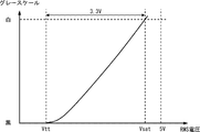
- FIG. 3 is a circuit diagram showing a specific configuration of an inverter constituting a first data holding unit provided in the pixel shown in FIG. 2. It is a schematic sectional drawing of the pixel shown in FIG. 2 is a timing chart illustrating an operation of the liquid crystal display device illustrated in FIG. 1. It is a figure which shows the relationship between the applied voltage (RMS voltage) of a liquid crystal, and the gray scale value of a liquid crystal.
- RMS voltage applied voltage
- FIG. 4 is a circuit diagram showing a specific configuration of a latch unit provided in the liquid crystal display device according to the concept prior to the first embodiment.
- FIG. FIG. 2 is a circuit diagram illustrating a specific configuration example of a latch unit provided in the liquid crystal display device illustrated in FIG. 1.
- 3 is a timing chart illustrating an operation of a latch unit provided in the liquid crystal display device illustrated in FIG. 1.
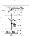
- FIG. 1 is a block diagram showing a liquid crystal display device 10 according to the first embodiment.
- the liquid crystal display device 10 includes an image display unit 11, a timing generator 13, a vertical shift register 14, a data latch circuit 15, and a horizontal driver 16.
- the horizontal driver 16 includes a horizontal shift register 161, a latch unit 162, and a level shifter / pixel driver 163.
- the image display unit 11 has a plurality of pixels 12 regularly arranged.
- the plurality of pixels 12 are connected to the vertical shift register 14 at one end and extend in the row direction (X direction) with m (m is a natural number of 2 or more) row scanning lines g1 to gm, and a level shifter / pixel driver 163.
- m is a natural number of 2 or more row scanning lines g1 to gm
- n column data lines d1 to dn a natural number of 2 or more
- All the pixels 12 in the image display unit 11 are commonly connected to trigger lines trig and trigb, one end of which is connected to the timing generator 13.
- the forward trigger pulse TRI transmitted by the forward trigger pulse trigger line trig and the inverted trigger pulse TRIB transmitted by the inverted trigger pulse trigger line trig are always in an inverse logical value relationship (complementary relationship). is there.
- the timing generator 13 receives external signals such as a vertical synchronization signal Vst, a horizontal synchronization signal Hst, and a basic clock CLK output from the host device 20 as input signals, and based on these external signals, AC signals FR, V Various internal signals such as a start pulse VST, an H start pulse HST, clock signals VCK and HCK, a latch pulse LT, and trigger pulses TRI and TRIB are generated.
- external signals such as a vertical synchronization signal Vst, a horizontal synchronization signal Hst, and a basic clock CLK output from the host device 20 as input signals, and based on these external signals, AC signals FR, V
- Various internal signals such as a start pulse VST, an H start pulse HST, clock signals VCK and HCK, a latch pulse LT, and trigger pulses TRI and TRIB are generated.
- the AC signal FR is a signal whose polarity is inverted every subframe, and is supplied to the common electrode of the liquid crystal display element in the pixel 12 constituting the image display unit 11 as a common electrode voltage Vcom described later.
- the start pulse VST is a pulse signal output at the start timing of each subframe described later, and switching of subframes is controlled by the start pulse VST.
- the start pulse HST is a pulse signal output to the horizontal shift register 161 at the start timing of the horizontal shift register 161.
- the clock signal VCK is a shift clock that defines one horizontal scanning period (1H) in the vertical shift register 14, and the vertical shift register 14 performs a shift operation at the timing of the clock signal VCK.
- the clock signal HCK is a shift clock in the horizontal shift register 161, and is a signal for shifting data with a 32-bit width.
- the latch pulse LT is a pulse signal that is output at a timing when the horizontal shift register 161 has finished shifting the data for the number of pixels in one row in the horizontal direction.
- the forward trigger pulse TRI and the inversion trigger pulse TRIB are pulse signals supplied to all the pixels 12 in the image display unit 11 via the trigger lines trig and trigb, respectively.
- the forward trigger pulse TRI and the inversion trigger pulse TRIB are output from the timing generator 13 after data is written in the first data holding units in all the pixels 12 in the image display unit 11 in a certain subframe period. Is done. Thereby, in the subframe period, the data held in the first data holding unit in all the pixels 12 in the image display unit 11 is transferred to the second data holding unit in the corresponding pixel 12 all at once.
- the vertical shift register 14 transfers the V start pulse VST supplied at the start timing of each subframe in accordance with the clock signal VCK, and sequentially supplies the row scanning signals to the row scanning lines g1 to gm sequentially in units of 1H. . Thereby, the row scanning lines are sequentially selected in units of 1H from the uppermost row scanning line g1 of the image display unit 11 to the lowermost row scanning line gm.
- the data latch circuit 15 latches 32-bit width data in units of one subframe supplied from an external circuit (not shown) based on the basic clock CLK from the host device 20, and then performs horizontal shift in synchronization with the basic clock CLK. Output to the register 161.
- the liquid crystal display device 10 divides one frame of the video signal into a plurality of subframes having a display period shorter than the one frame period of the video signal, and performs gradation display by combining these subframes. . Therefore, the external circuit converts the gradation data indicating the gradation of each pixel into a plurality of 1-bit subframe data corresponding to a plurality of subframes. Further, the external circuit collectively supplies the sub-frame data for 32 pixels belonging to the same sub-frame to the data latch circuit 15 as 32-bit width data.
- the horizontal shift register 161 When viewed as a 1-bit serial data processing system, the horizontal shift register 161 starts shifting by a start pulse HST supplied at the beginning of 1H from the timing generator 13, and 32-bit width data supplied from the data latch circuit 15. Are shifted in synchronization with the clock signal HCK.
- the latch unit 162 synchronizes with the latch pulse LT supplied from the timing generator 13
- Data of n bits (that is, subframe data of n pixels) supplied in parallel from the horizontal shift register 161 is latched and output to the level shifter of the level shifter / pixel driver 163.
- the start pulse HST is output again from the timing generator 13
- the horizontal shift register 161 resumes the 32-bit width data shift from the data latch circuit 15 in accordance with the clock signal HCK.
- the level shifter of the level shifter / pixel driver 163 shifts the signal level of n subframe data corresponding to n pixels in one row transferred from the latch unit 162 to the liquid crystal drive voltage amplitude.
- the pixel driver of the level shifter / pixel driver 163 outputs n pieces of subframe data corresponding to n pixels in one row after the level shift to n column data lines d1 to dn in parallel.
- the horizontal driver 16 outputs subframe data to pixels in a row selected as a data writing target in one horizontal scanning period, and outputs pixels in a row selected as a data writing target in the next one horizontal scanning period. Therefore, the subframe data is shifted in parallel. Then, in a certain horizontal scanning period, n subframe data corresponding to n pixels in one row are simultaneously output in parallel to the n column data lines d1 to dn as data signals.
- n pixels 12 in one row selected by the row scanning signal from the vertical shift register 14 are one row output from the level shifter / pixel driver 163 all at once.
- N subframe data are sampled via n column data lines d1 to dn and written in a first data holding unit (to be described later) in each pixel 12.
- the inverted data of the input data held in the storage unit SM1 is applied to the reflective electrode PE. That is, the pixel 12 has a function of inverting the input data supplied from the level shifter / pixel driver 163.
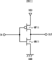
- FIG. 2 is a circuit diagram showing a specific configuration of the pixel 12.
- the pixel 12 has one of row scanning lines g1 to gm (hereinafter referred to as row scanning line g) and one of column data lines d1 to dn (hereinafter referred to as column data line d). ) And are provided at the intersection.
- the pixel 12 includes an SRAM cell 201, a DRAM cell 202, and a liquid crystal display element LC.
- the SRAM cell 201 includes a switch SW1 that is a first switch and a storage unit SM1 that is a first data holding unit.
- the DRAM cell 202 includes a switch SW2 that is a second switch and a storage unit DM2 that is a second data holding unit.
- the liquid crystal display element LC has a known structure in which a liquid crystal LCM is filled and enclosed in a space between a reflective electrode PE, which is a pixel electrode having light reflection characteristics arranged in a spaced-apart relationship, and a common electrode CE having light transmittance. It is.
- the switch SW1 is composed of, for example, an N-channel MOS transistor (hereinafter referred to as NMOS transistor) MN1.
- NMOS transistor MN1 N-channel MOS transistor
- the source is connected to the input terminal (node a) of the storage unit SM1
- the drain is connected to the column data line d
- the gate is connected to the row scanning line g.
- the storage unit SM1 is a self-holding memory composed of two inverters INV11 and INV12 having one output terminal connected to the other input terminal. More specifically, the input terminal of the inverter INV11 is connected to the output terminal of the inverter INV12 and the source of the NMOS transistor MN1 constituting the switch SW1. The input terminal of the inverter INV12 is connected to the switch SW2 and the output terminal of the inverter INV11.
- FIG. 3 is a circuit diagram showing a specific configuration of the inverter INV11.
- the inverter INV11 has a P-channel MOS transistor (hereinafter referred to as PMOS transistor) MP11 and an NMOS transistor MN11 connected in series, and inverts the input signals supplied to the respective gates.
- PMOS transistor P-channel MOS transistor
- MN11 NMOS transistor
- This is a well-known CMOS inverter that outputs from the drain of each of them.
- the inverter INV12 has a PMOS transistor MP12 and an NMOS transistor MN12 connected in series, and is a known CMOS inverter that inverts an input signal supplied to each gate and outputs it from each drain.
- the driving capabilities of the inverters INV11 and INV12 are different. Specifically, out of the inverters INV11 and INV12 constituting the storage unit SM1, the drive capability of the transistors MP11 and MN11 in the inverter INV11 on the input side when viewed from the switch SW1 is the inverter on the output side when viewed from the switch SW1. It is larger than the drive capability of the transistors MP12 and MN12 in the INV12. As a result, data easily propagates from the column data line d to the storage unit SM1 via the switch SW1, while data does not easily propagate from the storage unit DM2 to the storage unit SM1 via the switch SW2.
- the driving capability of the NMOS transistor MN1 constituting the switch SW1 is larger than the driving capability of the NMOS transistor MN12 constituting the inverter INV12. Accordingly, for example, when data indicating the H level on the column data line d is stored in the storage unit SM1, the current flowing from the column data line d to the input terminal (node a) of the storage unit SM1 via the switch SW1 is: Since the current flows from the input terminal of the storage unit SM1 to the ground voltage terminal GND via the NMOS transistor MN12, the data can be accurately stored in the storage unit SM1.
- the switch SW2 is a known transmission gate including an NMOS transistor MN2 and a PMOS transistor MP2 connected in parallel. More specifically, in the NMOS transistor MN2 and the PMOS transistor MP2, each source is commonly connected to the output terminal of the storage unit SM1, and each drain is connected to the input terminal of the storage unit DM2 and the reflective electrode PE of the liquid crystal display element LC. Commonly connected.
- the gate of the NMOS transistor MN2 is connected to the normal trigger pulse trigger line trig, and the gate of the PMOS transistor MP2 is connected to the inverted trigger pulse trigger line trigger.
- the switch SW2 is turned on when the normal rotation trigger pulse supplied via the trigger line trig is H level (the reverse trigger pulse supplied via the trigger line trigb is L level), and the switch SW2 is turned on.
- the read data is transferred to the storage unit DM2 and the reflective electrode PE.
- the switch SW2 is turned off when the normal rotation trigger pulse supplied via the trigger line trig is L level (the reverse trigger pulse supplied via the trigger line trigb is H level), and the switch SW2 The stored data is not read.
- the switch SW2 Since the switch SW2 is a known transmission gate, it can transfer a wide range of voltages from the ground voltage GND to the power supply voltage VDD in the on state. More specifically, when the voltage applied from the storage unit SM1 to the sources of the transistors MN2 and MP2 is the ground voltage GND level (L level), the source / drain of the PMOS transistor MP2 is not conducted, but the NMOS transistor MN2 The source / drain can be conducted with low resistance. On the other hand, when the voltage applied from the storage unit SM1 to the sources of the transistors MN2 and MP2 is the power supply voltage VDD level (H level), the source and drain of the PMOS transistor MP2 are It can conduct with low resistance. As described above, in the switch SW2, since the source and drain of the transmission gate can be conducted with low resistance, a wide range of voltages from the ground voltage GND to the power supply voltage VDD can be transferred in the on state.
- the storage unit DM2 is configured by a capacity C1.
- the capacitor C1 include a MIM (Metal Insulator Metal) capacitor that forms a capacitor between wirings, a Diffusion capacitor that forms a capacitor between a substrate and polysilicon, or a PIP (Poly) that forms a capacitor between two layers of polysilicon. Insulator Poly) capacity or the like can be used.
- the switch SW2 When the switch SW2 is turned on, the data stored in the storage unit SM1 is read and transferred to the capacitor C1 and the reflection electrode PE in the storage unit DM2 via the switch SW2. Thereby, the data stored in the storage unit DM2 is rewritten.
- the data held in the capacitor C1 also affects the input gate of the inverter INV12 constituting the storage unit SM1.
- the inverter INV11 since the drive capability of the inverter INV11 is larger than the drive capability of the inverter INV12, the inverter INV11 rewrites the data of the capacitor C1 before the inverter INV12 is affected by the data of the capacitor C1. Therefore, the data stored in the storage unit SM1 is not unintentionally rewritten by the data held in the capacitor C1.
- the liquid crystal display device 10 uses the pixel 12 including one SRAM cell and one DRAM cell, so that the pixel is more effective than the case where the pixel including two SRAM cells is used. By reducing the number of transistors that are configured, the size of the pixel is reduced.
- the switch SW2 includes the PMOS transistor MP2 and the NMOS transistor MN2 has been described, but the present invention is not limited to this.
- the switch SW2 can be appropriately changed to a configuration in which any one of the PMOS transistor MP2 and the NMOS transistor MN2 is provided. In that case, only one of the trigger lines trig, trigb is provided.
- the liquid crystal display device 10 can not only reduce the size of the pixel by reducing the number of transistors constituting the pixel, but also store the storage units SM1 and DM2 and the reflection electrode PE as described below. It is also possible to reduce the size of the pixels by arranging them effectively in the direction. Hereinafter, it demonstrates in detail using FIG.
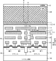
- FIG. 4 is a schematic cross-sectional view showing the main part of the pixel 12.
- FIG. 4 illustrates an example in which the capacitor C1 is configured by an MIM that forms a capacitor between wirings.
- an N well 101 and a P well 102 are formed on a silicon substrate 100.
- the PMOS transistor MP2 of the switch SW2 and the PMOS transistor MP11 of the inverter INV11 are formed on the N well 101. More specifically, a common diffusion layer serving as the source of each of the PMOS transistors MP2 and MP11 and two diffusion layers serving as the drain are formed on the N well 101, and the common diffusion layer, the two diffusion layers, Polysilicon serving as the gates of the PMOS transistors MP2 and MP11 is formed on the channel region between the two through a gate oxide film.
- an NMOS transistor MN2 of the switch SW2 and an NMOS transistor MN11 of the inverter INV11 are formed on the P well 102. More specifically, a common diffusion layer serving as the source of each of the NMOS transistors MN2 and MN11 and two diffusion layers serving as the drain are formed on the P well 102, and the common diffusion layer, the two diffusion layers, Polysilicon serving as the gates of the NMOS transistors MN2 and MN11 is formed on the channel region between the two through a gate oxide film.
- An element isolation oxide film 103 is formed between the active region (diffusion layer and channel region) on the N well and the active region on the P well.
- an interlayer insulating film 105 is interposed between the metals, the first metal 106, the second metal 108, the third metal 110, the MIM electrode 112, the fourth metal 114, and A fifth metal 116 is laminated.
- the fifth metal 116 constitutes a reflective electrode PE formed for each pixel.
- Each diffusion layer that constitutes each drain of the transistors MN2 and MP2 includes a contact 118, a first metal 106, a through hole 119a, a second metal 108, a through hole 119b, a third metal 110, a through hole 119c, a fourth metal 114, And, it is electrically connected to the fifth metal 116 through the through hole 119e. Further, each diffusion layer constituting each drain of the transistors MN2 and MP2 includes a contact 118, a first metal 106, a through hole 119a, a second metal 108, a through hole 119b, a third metal 110, a through hole 119c, and a fourth metal. 114 and the through hole 119d are electrically connected to the MIM electrode 112. That is, the sources of the transistors MN2 and MP2 constituting the switch SW2 are electrically connected to the reflective electrode PE and the MIM electrode 112.
- the reflective electrode PE (fifth metal 116) is disposed so as to be opposed to the common electrode CE, which is a transparent electrode, via a passivation film (PSV) 117, which is a protective film formed on the upper surface thereof.
- a liquid crystal LCM is filled and sealed between the reflective electrode PE and the common electrode CE.
- a liquid crystal display element LC is configured by the reflective electrode PE, the common electrode CE, and the liquid crystal LCM therebetween.
- the MIM electrode 112 is formed on the third metal 110 via the interlayer insulating film 105.
- the MIM electrode 112, the third metal 110, and the interlayer insulating film 105 between them constitute a capacitor C1. Therefore, the switches SW1 and SW2 and the storage unit SM1 are formed using the first metal 106 and the second metal 108, which are the first and second layer wirings, and the transistor, whereas the storage unit DM2 It is formed using the third metal 110 and the MIM electrode 112 which are upper layers. That is, the switches SW1 and SW2, the storage unit SM1, and the storage unit DM2 are formed in different layers.
- Light from a light source passes through the common electrode CE and the liquid crystal LCM, is incident on the reflective electrode PE (fifth metal 116), is reflected, and travels backward through the original incident path and is emitted through the common electrode CE. .
- the liquid crystal display device 10 uses the fifth metal 116 that is the fifth layer wiring as the reflective electrode PE, the third metal 110 that is the third layer wiring as a part of the memory unit DM2,
- the first metal 106 and the second metal 108 which are two-layer wiring, and the transistor as the memory unit SM1, etc.
- the pixel can be further reduced in size.
- pixels with a pitch of 3 ⁇ m or less can be configured with transistors having a power supply voltage of 3.3V.
- a liquid crystal display panel having a diagonal length of 0.55 inches and a horizontal direction of 4000 pixels and a vertical direction of 2000 pixels can be realized.
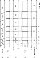
- FIG. 5 is a timing chart showing the operation of the liquid crystal display device 10.
- the row scanning lines g 1 to gm are sequentially selected in units of 1H by the row scanning signal from the vertical shift register 14. Data is written to each pixel 12 in units of n pixels in one row commonly connected to the selected row scanning line. Then, when data is written in all of the plurality of pixels 12 constituting the image display unit 11, thereafter, the data of all the pixels 12 are simultaneously read based on the trigger pulses TRI and TRIB (more specifically, Data in the storage unit SM1 in all the pixels 12 is transferred to the storage unit DM2 and the reflective electrode PE all at once).
- FIG. 5 shows changes in subframe data stored in each pixel 12.
- the vertical axis represents the row number, and the horizontal axis represents time.
- the boundary line of the subframe data has a lower right side. This indicates that the sub-frame data is written later as the pixel having a larger row number.
- a period from one end to the other end of the boundary line corresponds to a subframe data writing period.
- B0b, B1b, and B2b indicate inverted data of subframe data of bits B0, B1, and B2, respectively.
- FIG. 5B shows the output timing (rise timing) of the trigger pulse TRI.
- the trigger pulse TRIB is omitted because it always indicates a logically inverted value of the trigger pulse TRI.
- FIG. 5C schematically shows the bits of the subframe data applied to the reflective electrode PE.
- FIG. 5D shows a change in the value of the common electrode voltage Vcom.
- FIG. 5E shows a change in voltage applied to the liquid crystal LCM.
- the switch SW1 is turned on, so that the normal subframe data of the bit B0 output from the horizontal driver 16 to the column data line d is sampled by the switch SW1 and stored in the storage unit.
- SM1 normal rotation subframe data of bit B0 is written in the storage unit SM1 of all the pixels 12 constituting the image display unit 11.
- the H level trigger pulse TRI and the L level trigger pulse TRIB is simultaneously supplied to all the pixels 12 constituting the image display unit 11 (time T1).
- the switches SW2 of all the pixels 12 are turned on, so that the normal subframe data of the bit B0 stored in the storage unit SM1 is transferred to the storage unit DM2 all at once through the switch SW2 and held.
- B0 normal rotation subframe data is applied to the reflective electrode PE.
- the retention period of the normal subframe data of bit B0 by the storage unit DM2 (application period of the normal subframe data of bit B0 to the reflective electrode PE). Is one subframe period from the time when the trigger pulse TRI becomes H level (time T1) to the time when it again becomes H level (time T2).
- the power supply voltage VDD (3.3 V in this case) is applied to the reflective electrode PE
- the bit value is “0”, that is, L level.
- a ground voltage GND (0 V) is applied to the reflective electrode PE.
- a free voltage can be applied to the common electrode CE as the common electrode voltage Vcom without being limited to the ground voltage GND and the power supply voltage VDD.
- the common electrode voltage Vcom is controlled to be switched to a predetermined voltage in synchronization.
- the common electrode voltage Vcom is equal to the threshold voltage Vtt of the liquid crystal rather than 0V, as shown in FIG. 5D, during the subframe period in which the normal subframe data of bit B0 is applied to the reflective electrode PE. Set to low voltage.
- FIG. 6 shows the relationship between the applied voltage (RMS voltage) of the liquid crystal and the gray scale value of the liquid crystal.
- the storage unit SM1 of all the pixels 12 constituting the image display unit 11 is stored. Writing of the inverted subframe data of bit B0 is sequentially started. When the inverted subframe data of bit B0 is written to the storage unit SM1 of all the pixels 12 constituting the image display unit 11, the H level is then applied to all the pixels 12 constituting the image display unit 11. Trigger pulse TRI (and L level trigger pulse TRIB) are simultaneously supplied (time T2).
- the switches SW2 of all the pixels 12 are turned on, so that the inverted subframe data of the bit B0 stored in the storage unit SM1 is simultaneously transferred to and held in the storage unit DM2 through the switch SW2, and the bit B0
- the inverted subframe data is applied to the reflective electrode PE.
- the retention period of the inverted subframe data of bit B0 by the storage unit DM2 is as follows. This is one subframe period from the time when the trigger pulse TRI becomes H level (time T2) to the time when it again becomes H level (time T3).
- the inverted subframe data of bit B0 is always in an inverse logical value relationship with the normal subframe data of bit B0, when the normal subframe data of bit B0 is “1”, “0” When the normal rotation subframe data of B0 is “0”, it is “1”.
- the common electrode voltage Vcom is higher than the 3.3V threshold voltage Vtt as shown in FIG. 5D during the subframe period in which the inverted subframe data of the bit B0 is applied to the reflective electrode PE.
- the bit value of the normal subframe data of bit B0 is “1”
- the bit value of the inverted subframe data of bit B0 applied subsequently is “0”.
- the applied voltage of the liquid crystal LCM is ⁇ (3.3V + Vtt), and the potential direction is reversed but the absolute value is the same as compared to when the normal rotation subframe data of the bit B0 is applied. . Therefore, the pixel 12 displays white when the inverted subframe data of the bit B0 is applied, similarly to when the normal frame data of the bit B0 is applied.
- the bit value of the normal subframe data of bit B0 is “0”
- the bit value of the inverted subframe data of bit B0 applied subsequently is “1”.
- the voltage applied to the liquid crystal LCM is ⁇ Vtt, and the potential direction is reversed but the absolute value is the same as when the normal subframe data of the bit B0 is applied. Therefore, the pixel 12 displays black when the inverted subframe data of the bit B0 is applied, similarly to when the normal frame data of the bit B0 is applied.
- the pixel 12 displays the same gradation in the bit B0 and the complementary bit B0b of the bit B0 during the two subframe periods from time T1 to time T3, and the liquid crystal LCM Since AC driving in which the potential direction is reversed for each subframe is performed, burn-in of the liquid crystal LCM can be prevented.
- the normal subframe data of bit B1 is written to the storage unit SM1 of all the pixels 12.
- the H level trigger is then applied to all the pixels 12 constituting the image display unit 11.
- the pulse TRI (and the L level trigger pulse TRIB) is simultaneously supplied (time T3).
- the switches SW2 of all the pixels 12 are turned on, so that the normal subframe data of the bit B1 stored in the storage unit SM1 is transferred to the storage unit DM2 all at once through the switch SW2, and held.
- the normal rotation subframe data of bit B1 is applied to the reflective electrode PE.
- the retention period of the normal subframe data of bit B1 by the storage unit DM2 Is one subframe period from the time when the trigger pulse TRI becomes H level (time T3) to the time when it again becomes H level (time T4).
- the switches SW2 of all the pixels 12 are turned on, so that the inverted subframe data of the bit B1 stored in the storage unit SM1 is transferred and held all at once to the storage unit DM2 through the switch SW2, and the bit B1
- the inverted subframe data is applied to the reflective electrode PE.
- the retention period of the inverted subframe data of the bit B1 by the storage unit DM2 is: This is one subframe period from when the trigger pulse TRI becomes H level (time T4) until it becomes H level again (time T5).
- the inverted subframe data of bit B1 is always in the relationship of the inverse logical value with the normal subframe data of bit B1.
- the common electrode voltage Vcom is higher than the 3.3V threshold voltage Vtt as shown in FIG. 5D during the subframe period in which the inverted subframe data of the bit B1 is applied to the reflective electrode PE.
- the pixel 12 displays the same gradation in the bit B1 and the complementary bit B1b of the bit B1 and the liquid crystal LCM during the two subframes from time T3 to T5. Since the alternating current driving in which the potential direction is inverted every subframe, the burn-in of the liquid crystal LCM can be prevented. The same operation is repeated for bits B2 and thereafter.
- the liquid crystal display device 10 performs gradation display using a combination of a plurality of subframes.
- the display periods of bit B0 and complementary bit B0b are the same first subframe period, and the display periods of bit B1 and complementary bit B1b are also the same second subframe period.
- the subframe period and the second subframe period are not necessarily the same.
- the second subframe period is set to be twice the first subframe period.
- the third subframe period which is the display period of the bit B2 and the complementary bit B2b, is set to be twice the second subframe period. The same can be said for other subframe periods.
- the length of each subframe period and the number of subframes can be arbitrarily set according to the system specifications and the like.
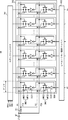
- FIG. 7 is a circuit diagram showing a specific configuration of the latch unit 562 according to the concept before reaching the first embodiment. 7 also shows a horizontal shift register 161 and a level shifter / pixel driver 163 which are peripheral circuits of the latch unit 562.
- the latch unit 562 includes n latch circuits 564 corresponding to n columns of the plurality of pixels 12 arranged in a matrix.
- Each of the n latch circuits 564 is disposed opposite to the n pixels 12 arranged in the row direction, and has a pitch (width in the row direction) corresponding to the pitch of the n pixels 12. Yes.
- the latch unit 562 is supplied with pulse signals P1, P1b, P2, and P2b obtained by normalizing or inverting the latch pulse LT from the timing generator 13. More specifically, the latch unit 562 is supplied with pulse signals P1 and P2b obtained by normalizing the latch pulse LT by the buffer BF1, and pulse signals P1b and P2 obtained by inverting the latch pulse LT by the inverter IV1. Supplied.
- the switch SW21 is a known transmission gate including an NMOS transistor MN21 and a PMOS transistor MP21 connected in parallel. More specifically, in the NMOS transistor MN21 and the PMOS transistor MP21, each source is commonly connected to a corresponding output terminal in the horizontal shift register 161, and each drain is commonly connected to an input terminal of the inverter IV21.
- a pulse signal P1 is supplied to the gate of the NMOS transistor MN21, and a pulse signal P1b that is an inverted signal of the pulse signal P1 is supplied to the gate of the PMOS transistor MP21.
- the output terminal of the inverter IV21 is connected to the input terminal of the inverter IV22 and the corresponding input terminal of the level shifter / pixel driver 163.
- the switch SW22 is a known transmission gate including an NMOS transistor MN22 and a PMOS transistor MP22 connected in parallel. More specifically, in the NMOS transistor MN22 and the PMOS transistor MP22, the respective sources are commonly connected to the output terminal of the inverter IV22, and the respective drains are commonly connected to the input terminal of the inverter IV21.
- a pulse signal P2 is supplied to the gate of the NMOS transistor MN22, and a pulse signal P2b that is an inverted signal of the pulse signal P2 is supplied to the gate of the PMOS transistor MP22.
- the pulse signals P1 and P2b indicate the L level and the pulse signals P1b and P2 indicate the H level, so that the switch SW21 is turned off and the switch SW22 is turned on.
- the pulse signals P1 and P2b indicate the H level and the pulse signals P1b and P2 indicate the L level, so that the switch SW21 is turned on and the switch SW22 is turned off.
- the latch pulse LT indicates the L level. Accordingly, since the pulse signals P1 and P2b indicate the L level and the pulse signals P1b and P2 indicate the H level, the switch SW21 is turned off and the switch SW22 is turned on.
- the horizontal shift register 161 starts shifting by the start pulse HST supplied from the timing generator 13 at the beginning of 1H, and is supplied from the data latch circuit 15 as 32 bits. The width data is shifted in synchronization with the clock signal HCK.
- the latch pulse LT rises (switches from L level to H level).
- the pulse signals P1 and P2b rise (switch from L level to H level) and the pulse signals P1b and P2 fall (switch from H level to L level), so the switch SW21 is turned on and the switch SW22 is turned off.
- n-bit data that is, sub-frame data for n pixels
- the level shifter of the level shifter / pixel driver 163 shifts the signal level of n subframe data corresponding to n pixels in one row transferred from the latch unit 562 to the liquid crystal drive voltage amplitude.
- the pixel driver of the level shifter / pixel driver 163 outputs n subframe data corresponding to n pixels in one row after the level shift to n column data lines d1 to dn in parallel. That is, in a certain horizontal scanning period, n subframe data corresponding to n pixels in one row are simultaneously output in parallel to n column data lines d1 to dn as data signals.
- the latch pulse LT falls. Accordingly, the pulse signals P1 and P2b fall and the pulse signals P1b and P2 rise, so that the switch SW21 is turned off and the switch SW22 is turned on. Accordingly, the latch unit 562 is disconnected from the horizontal shift register 161, but continues to hold the sub-frame data for n pixels supplied from the horizontal shift register 161 until immediately before. Therefore, the latch unit 562 can continue to output the sub-frame data for the n pixels in parallel to the n column data lines d1 to dn.
- next 1H start pulse HST is supplied from the timing generator 13 to the horizontal shift register 161 during the period when the latch pulse LT is at the L level. Accordingly, the horizontal shift register 161 resumes the operation of shifting the 32-bit width data supplied from the data latch circuit 15.
- the horizontal driver 56 outputs the subframe data toward the pixel of the row selected as the data writing target in one horizontal scanning period and the pixel of the row selected as the data writing target in the next horizontal scanning period.
- the subframe data is shifted in parallel with the above.
- n sub-frame data directed to the n pixels 12 are parallel and simultaneously to the n column data lines d1 to dn in synchronization with the rising edge of the latch pulse LT. Is output. Accordingly, in the liquid crystal display device equipped with the latch unit 562, the current flowing from the power supply voltage terminal to the ground voltage terminal increases momentarily (that is, the peak current consumption increases), and thus the power supply voltage VDD decreases. There is a problem that an IR drop phenomenon occurs in which the ground voltage GND increases. As a result, in the liquid crystal display device equipped with the latch unit 562, for example, a malfunction may occur or the image quality may deteriorate.
- the latch unit 162 and the liquid crystal display device 10 equipped with the latch unit 162 have been found so that the IR drop can be prevented by suppressing the peak current consumption.
- FIG. 8 is a circuit diagram illustrating a specific configuration example of the latch unit 162 according to the first embodiment. 8 also shows a horizontal shift register 161 and a level shifter / pixel driver 163, which are peripheral circuits of the latch unit 162.
- the latch unit 162 includes n latch circuits 164 provided corresponding to n columns of the plurality of pixels 12 arranged in a matrix.
- Each of the n latch circuits 164 is arranged to face the n pixels 12 arranged in the row direction, and has a pitch (width in the row direction) corresponding to the pitch of the n pixels 12. Yes.
- the latch unit 162 includes delay buffers D1L, D1bL, D2L, D2bL, and delay buffers D1R, D1bR, D2R, D2bR. These delay buffers serve as a timing adjustment circuit that adjusts the supply timing of subframe data to each of the n pixels 12 provided in each row of the plurality of pixels 12. Details will be described later.
- n latch circuits 164 are divided into a plurality of latch circuit groups.
- n latch circuits 164 include n / 3 latch circuits 164 (latch circuit group 1642) arranged in the center, and the negative side in the row direction (left side of the drawing) than latch circuit group 1642.
- N / 3 latch circuits 164 (latch circuit group 1641) arranged in the n, and n / 3 latch circuits 164 (latch circuits) arranged on the positive side in the row direction (right side of the drawing) from the latch circuit group 1642 Group 1643).
- the latch circuit group 1642 provided in the center of the latch unit 162 is supplied with pulse signals P1, P1b, P2, and P2b obtained by normal rotation or inversion of the latch pulse LT from the timing generator 13. More specifically, the latch circuit group 1642 is supplied with pulse signals P1 and P2b obtained by normalizing the latch pulse LT by the buffer BF1, and pulse signals P1b and P2 obtained by inverting the latch pulse LT by the inverter IV1. Is supplied.
- the latch circuit group 1641 provided in the left region of the latch unit 162 includes pulse signals P1L, P1bL obtained by delaying the pulse signals P1, P1b, P2, P2b using delay buffers D1L, D1bL, D2L, D2bL, respectively. , P2L, P2bL are supplied.
- the latch circuit group 1643 provided in the right region of the latch unit 162 includes pulse signals P1R, P1bR obtained by delaying the pulse signals P1, P1b, P2, P2b using the delay buffers D1R, D1bR, D2R, D2bR, respectively. , P2R, P2bR are supplied.
- the switch SW21 is a known transmission gate including an NMOS transistor MN21 and a PMOS transistor MP21 connected in parallel. More specifically, in the NMOS transistor MN21 and the PMOS transistor MP21, each source is commonly connected to a corresponding output terminal in the horizontal shift register 161, and each drain is commonly connected to an input terminal of the inverter IV21.
- a pulse signal P1 is supplied to the gate of the NMOS transistor MN21, and a pulse signal P1b that is an inverted signal of the pulse signal P1 is supplied to the gate of the PMOS transistor MP21.
- the output terminal of the inverter IV21 is connected to the input terminal of the inverter IV22 and the corresponding input terminal of the level shifter / pixel driver 163.
- the switch SW22 is a known transmission gate including an NMOS transistor MN22 and a PMOS transistor MP22 connected in parallel. More specifically, in the NMOS transistor MN22 and the PMOS transistor MP22, the respective sources are commonly connected to the output terminal of the inverter IV22, and the respective drains are commonly connected to the input terminal of the inverter IV21.
- a pulse signal P2 is supplied to the gate of the NMOS transistor MN22, and a pulse signal P2b that is an inverted signal of the pulse signal P2 is supplied to the gate of the PMOS transistor MP22.
- the switch SW21 is turned off and the switch SW22 is turned on.
- the pulse signals P1 and P2b indicate the H level
- the pulse signals P1b and P2 indicate the L level.
- each latch circuit 164 of the latch circuit group 1641 provided in the left region of the latch unit 162 the pulse signal P1L is supplied to the gate of the NMOS transistor MN21, and the inverted signal of the pulse signal P1L is supplied to the gate of the PMOS transistor MP21.
- the pulse signal P1bL is supplied.
- a pulse signal P2L is supplied to the gate of the NMOS transistor MN22, and a pulse signal P2bL that is an inverted signal of the pulse signal P2L is supplied to the gate of the PMOS transistor MP22.
- the other configuration of each latch circuit 164 in the latch circuit group 1641 is the same as the configuration of each latch circuit 164 in the latch circuit group 1642, and thus description thereof is omitted.
- the pulse signals P1, P2b indicate the L level
- the pulse signals P1b, P2 indicate the H level
- the pulse signals P1L, P2bL are L level is indicated
- the pulse signals P1bL and P2L indicate H level. Accordingly, in each latch circuit 164 of the latch circuit group 1641, the switch SW21 is turned off and the switch SW22 is turned on.
- the pulse signals P1 and P2b indicate the H level
- the pulse signals P1b and P2 indicate the L level
- the pulse signals P1L and P2bL are The H level is indicated
- the pulse signals P1bL and P2L indicate the L level. Accordingly, in each latch circuit 164 of the latch circuit group 1641, the switch SW21 is turned on and the switch SW22 is turned off.
- each latch circuit 164 of the latch circuit group 1643 provided in the right region of the latch unit 162, the pulse signal P1R is supplied to the gate of the NMOS transistor MN21, and the inverted signal of the pulse signal P1R is supplied to the gate of the PMOS transistor MP21.
- a pulse signal P1bR is supplied.
- the pulse signal P2R is supplied to the gate of the NMOS transistor MN22, and the pulse signal P2bR that is an inverted signal of the pulse signal P2R is supplied to the gate of the PMOS transistor MP22.
- the other configuration of each latch circuit 164 in the latch circuit group 1643 is the same as the configuration of each latch circuit 164 in the latch circuit group 1642, and thus description thereof is omitted.
- the pulse signals P1 and P2b indicate the L level
- the pulse signals P1b and P2 indicate the H level
- the pulse signals P1R and P2bR are The L level is indicated
- the pulse signals P1bR and P2R indicate the H level. Accordingly, in each latch circuit 164 of the latch circuit group 1643, the switch SW21 is turned off and the switch SW22 is turned on.
- the pulse signals P1 and P2b indicate the H level
- the pulse signals P1b and P2 indicate the L level
- the pulse signals P1R and P2bR are The H level is indicated
- the pulse signals P1bR and P2R indicate the L level. Accordingly, in each latch circuit 164 of the latch circuit group 1643, the switch SW21 is turned on and the switch SW22 is turned off.
- signal lines through which the pulse signals P1, P1b, P2, and P2b propagate are mainly wired to a wiring layer (for example, an upper wiring layer) different from the wiring layer that constitutes the latch circuit 164.
- the signal line through which the pulse signals P1L, P1bL, P2L, and P2bL propagate and the signal line through which the pulse signals P1R, P1bR, P2R, and P2bR propagate are mainly different from the wiring layers that constitute the latch circuit 164. It is partially disposed on a wiring layer (for example, an upper wiring layer).
- the delay buffers D1L, D1bL, D2L, D2bL and the delay buffers D1R, D1bR, D2R, D2bR are all formed in a region different from the region constituting the latch circuit 164 (for example, the upper side in FIG. 8).
- the n latch circuits 164 can be arranged to face the n pixels 12 arranged in the row direction without being affected by the delay buffer and without disturbing the pitch. Thereby, the liquid crystal display device 10 can display the entire image displayed on the image display unit 11 uniformly.
- the delay buffer is arranged in a different area from the latch circuit 164, the size and the number of stages can be changed with a high degree of freedom.
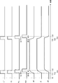
- FIG. 9 is a timing chart showing the operation of the latch unit 162.
- FIG. 9 shows an example in which “1” is written to the n pixels 12 in the first row and “0” is written to the n pixels 12 in the second row.
- the latch pulse LT indicates the L level (time T0). Accordingly, since the pulse signals P1 and P2b indicate the L level and the pulse signals P1b and P2 indicate the H level, in each latch circuit 164 of the latch circuit group 1642, the switch SW21 is turned off and the switch SW22 is turned on. . Further, since the pulse signals P1L and P2bL indicate the L level and the pulse signals P1bL and P2L indicate the H level, in each latch circuit 164 of the latch circuit group 1641, the switch SW21 is turned off and the switch SW22 is turned on. Further, since the pulse signals P1R and P2bR indicate L level and the pulse signals P1bR and P2R indicate H level, in each latch circuit 164 of the latch circuit group 1643, the switch SW21 is turned off and the switch SW22 is turned on.
- the level shifter of the level shifter / pixel driver 163 shifts the level of the n / 3 subframe data transferred from the latch unit 162 to the liquid crystal drive voltage amplitude.
- the pixel driver of the level shifter / pixel driver 163 converts the n / 3 subframe data after the level shift into n / 3 column data lines d () corresponding to the latch circuits 164 of the latch circuit group 1642.
- the data is output in parallel to the column data line group dM). Thereby, the voltage level of each column data line d of the column data line group dM is switched from the L level to the H level (time T11).
- the pulse signals P1 and P2b rise and the pulse signals P1b and P2 fall the pulse signals P1L and P2bL rise and the pulse signals P1bL and P2L fall after a predetermined delay time (time T12). Accordingly, in each latch circuit 164 of the latch circuit group 1641, the switch SW21 is turned on and the switch SW22 is turned off. Accordingly, n / 3 subframe data corresponding to each latch circuit 164 of the latch circuit group 1641 out of the subframe data for n pixels in the first row output from the horizontal shift register 161 is converted into level shifters / pixels. It is transferred to the driver 163.
- the level shifter of the level shifter / pixel driver 163 shifts the level of the n / 3 subframe data transferred from the latch unit 162 to the liquid crystal drive voltage amplitude.
- the pixel driver of the level shifter / pixel driver 163 converts the n / 3 subframe data after the level shift into n / 3 column data lines d () corresponding to the latch circuits 164 of the latch circuit group 1641.
- the data is output in parallel to the column data line group dL).
- the voltage level of each column data line d in the column data line group dL is switched from the L level to the H level (time T12).
- FIG. 9 shows a case where the delay buffers D1R, D1bR, D2R, D2bR in FIG. 8 are delayed from the delay buffers D1L, D1bL, D2L, D2bL. This is because the peak current consumption is reduced by reducing the number of circuits operating at one time by making the left and right delay times different.
- the delay buffers D1R, D1bR, D2R, and D2bR can be set to the same delay time as the delay buffers D1L, D1bL, D2L, and D2bL. Accordingly, in each latch circuit 164 of the latch circuit group 1643, the switch SW21 is turned on and the switch SW22 is turned off. Accordingly, n / 3 subframe data corresponding to each latch circuit 164 of the latch circuit group 1643 among the subframe data for n pixels in the first row output from the horizontal shift register 161 is converted into level shifters / pixels. It is transferred to the driver 163.
- the level shifter of the level shifter / pixel driver 163 shifts the level of the n / 3 subframe data transferred from the latch unit 162 to the liquid crystal drive voltage amplitude.
- the pixel driver of the level shifter / pixel driver 163 converts the n / 3 subframe data after the level shift into n / 3 column data lines d (provided corresponding to the latch circuits 164 of the latch circuit group 1643).
- the data is output in parallel to the column data line group dR).
- the voltage level of each column data line d in the column data line group dR is switched from the L level to the H level (time T13).
- the latch pulse LT falls (time T14).
- the latch unit 162 is disconnected from the horizontal shift register 161, but continues to hold the sub-frame data for n pixels supplied from the horizontal shift register 161 until immediately before. Therefore, the latch unit 162 can continue to output the sub-frame data for the n pixels in parallel to the n column data lines d1 to dn. As a result, the voltage levels of the n column data lines d1 to dn are maintained at the H level.
- the level shifter of the level shifter / pixel driver 163 shifts the level of the n / 3 subframe data transferred from the latch unit 162 to the liquid crystal drive voltage amplitude.
- the pixel driver of the level shifter / pixel driver 163 converts the n / 3 subframe data after the level shift into n / 3 column data lines d () corresponding to the latch circuits 164 of the latch circuit group 1642.
- the data is output in parallel to the column data line group dM). Thereby, the voltage level of each column data line d in the column data line group dM is switched from the H level to the L level (time T21).
- the pulse signals P1 and P2b rise and the pulse signals P1b and P2 fall the pulse signals P1L and P2bL rise and the pulse signals P1bL and P2L fall after a predetermined delay time (time T22). Accordingly, in each latch circuit 164 of the latch circuit group 1641, the switch SW21 is turned on and the switch SW22 is turned off. Accordingly, n / 3 subframe data corresponding to each latch circuit 164 of the latch circuit group 1641 out of the subframe data for n pixels in the second row output from the horizontal shift register 161 is converted into level shifters / pixels. It is transferred to the driver 163.
- the level shifter of the level shifter / pixel driver 163 shifts the level of the n / 3 subframe data transferred from the latch unit 162 to the liquid crystal drive voltage amplitude.
- the pixel driver of the level shifter / pixel driver 163 converts the n / 3 subframe data after the level shift into n / 3 column data lines d () corresponding to the latch circuits 164 of the latch circuit group 1641.
- the data is output in parallel to the column data line group dL). Thereby, the voltage level of each column data line d of the column data line group dL is switched from the H level to the L level (time T22).
- the pulse signals P1 and P2b rise and the pulse signals P1b and P2 fall the pulse signals P1R and P2bR rise and the pulse signals P1bR and P2R fall after a predetermined delay time (time T23). Accordingly, in each latch circuit 164 of the latch circuit group 1643, the switch SW21 is turned on and the switch SW22 is turned off. Accordingly, n / 3 subframe data corresponding to each latch circuit 164 of the latch circuit group 1643 out of the subframe data for n pixels in the second row output from the horizontal shift register 161 is converted into level shifters / pixels. It is transferred to the driver 163.
- the level shifter of the level shifter / pixel driver 163 shifts the level of the n / 3 subframe data transferred from the latch unit 162 to the liquid crystal drive voltage amplitude.
- the pixel driver of the level shifter / pixel driver 163 converts the n / 3 subframe data after the level shift into n / 3 column data lines d (provided corresponding to the latch circuits 164 of the latch circuit group 1643).
- the data is output in parallel to the column data line group dR). Thereby, the voltage level of each column data line d in the column data line group dR is switched from the H level to the L level (time T23).
- the latch pulse LT falls (time T24).
- the latch unit 162 is disconnected from the horizontal shift register 161, but continues to hold the sub-frame data for n pixels supplied from the horizontal shift register 161 until immediately before. Therefore, the latch unit 162 can continue to output the sub-frame data for the n pixels in parallel to the n column data lines d1 to dn. As a result, the voltage levels of the n column data lines d1 to dn are maintained at the L level.
- the delay time XL from time T11 to time T12 and the delay time XL from time T21 to time T22 can be adjusted by changing the size and the number of stages of the delay buffers D1L, D1bL, D2L, and D2bL.
- the delay time XR from time T11 to time T13 and the delay time XR from time T21 to time T23 can be adjusted by changing the size and the number of stages of the delay buffers D1R, D1bR, D2R, D2bR.
- the circuit configuration is not complicated as compared with the configuration in which the delay times XL and XR are adjusted in synchronization with the operation clock, and the cycle of the operation clock.
- the delay times XL and XR can be adjusted with finer precision.
- the liquid crystal display device includes a timing adjustment circuit that adjusts the supply timing of n subframe data to each of the n pixels 12 provided in each row.
- the timing adjustment circuit is, for example, a delay buffer, and subframe data for some column data lines among n column data lines provided corresponding to n pixels 12 provided in each row.
- the supply timing is different from the supply timing of subframe data to some other column data lines.
- the delay buffer is arranged in a different area from the n latch circuits 164. Therefore, the n latch circuits 164 can be arranged to face the n pixels 12 arranged in the row direction without being affected by the delay buffer and without disturbing the pitch. Thereby, the liquid crystal display device 10 according to the present embodiment can uniformly display the entire image displayed on the image display unit 11 without unevenness.
- the delay buffer is arranged in a different area from the n latch circuits 164, the size and the number of stages can be changed with a high degree of freedom.
- a large number of delay buffers are arranged in advance, and a timing adjustment circuit is configured using only the required number of delay buffers. After that, for example, when a problem occurs, an unused delay buffer is replaced.
- the timing adjustment circuit can be reconfigured. Alternatively, when timing adjustment is unnecessary, a timing adjustment circuit using a delay buffer may not be configured.
- n latch circuits 164 are divided into three latch circuit groups, and the subframe data supply timings by the three latch circuit groups are different from each other.
- the n latch circuits 164 can be divided into two or more arbitrary number of latch circuit groups, and the sub-frame data supply timing by these latch circuit groups can be changed appropriately.
- the peak current consumption can be more effectively suppressed as the number of latch circuits constituting one latch circuit group is reduced and the number of latch circuit groups as timing control units is increased.
- the number of latch circuits constituting one latch circuit group is increased and the number of latch circuit groups as timing control units is decreased, an increase in delay time due to the delay buffer can be suppressed.
- the operating time per 1H of the driver 16 can be easily kept within the allowable time. If the operation time per 1H of the horizontal driver 16 cannot be kept within the allowable time for a prototype wafer, the size and number of stages of the delay buffer are changed, or the wiring pattern is changed. Thus, it is possible to adjust the operating time per 1 H of the horizontal driver 16 within an allowable range.
- the present invention is not limited to this.
- the number of latch circuits constituting each of the latch circuit groups 1641 to 1643 may be different.
- the present invention can be suitably applied to a liquid crystal display device mounted on a projector or the like.
Landscapes
- Physics & Mathematics (AREA)
- Engineering & Computer Science (AREA)
- Nonlinear Science (AREA)
- General Physics & Mathematics (AREA)
- Chemical & Material Sciences (AREA)
- Crystallography & Structural Chemistry (AREA)
- Optics & Photonics (AREA)
- Mathematical Physics (AREA)
- Computer Hardware Design (AREA)
- Theoretical Computer Science (AREA)
- Microelectronics & Electronic Packaging (AREA)
- Control Of Indicators Other Than Cathode Ray Tubes (AREA)
- Liquid Crystal (AREA)
- Liquid Crystal Display Device Control (AREA)
Priority Applications (1)
| Application Number | Priority Date | Filing Date | Title |
|---|---|---|---|
| US16/289,431 US20190197938A1 (en) | 2016-08-31 | 2019-02-28 | Liquid crystal display apparatus |
Applications Claiming Priority (2)
| Application Number | Priority Date | Filing Date | Title |
|---|---|---|---|
| JP2016168951A JP6774599B2 (ja) | 2016-08-31 | 2016-08-31 | 液晶表示装置 |
| JP2016-168951 | 2016-08-31 |
Related Child Applications (1)
| Application Number | Title | Priority Date | Filing Date |
|---|---|---|---|
| US16/289,431 Continuation US20190197938A1 (en) | 2016-08-31 | 2019-02-28 | Liquid crystal display apparatus |
Publications (1)
| Publication Number | Publication Date |
|---|---|
| WO2018042711A1 true WO2018042711A1 (ja) | 2018-03-08 |
Family
ID=61300370
Family Applications (1)
| Application Number | Title | Priority Date | Filing Date |
|---|---|---|---|
| PCT/JP2017/007313 Ceased WO2018042711A1 (ja) | 2016-08-31 | 2017-02-27 | 液晶表示装置 |
Country Status (3)
| Country | Link |
|---|---|
| US (1) | US20190197938A1 (enExample) |
| JP (1) | JP6774599B2 (enExample) |
| WO (1) | WO2018042711A1 (enExample) |
Cited By (1)
| Publication number | Priority date | Publication date | Assignee | Title |
|---|---|---|---|---|
| WO2020017259A1 (ja) * | 2018-07-18 | 2020-01-23 | 株式会社ジャパンディスプレイ | 表示装置 |
Families Citing this family (2)
| Publication number | Priority date | Publication date | Assignee | Title |
|---|---|---|---|---|
| JP6870596B2 (ja) * | 2017-11-30 | 2021-05-12 | 株式会社Jvcケンウッド | 液晶表示装置及びその駆動方法 |
| KR20230146697A (ko) * | 2022-04-12 | 2023-10-20 | 삼성디스플레이 주식회사 | 데이터 구동 회로 및 그것을 포함하는 표시 장치 |
Citations (8)
| Publication number | Priority date | Publication date | Assignee | Title |
|---|---|---|---|---|
| JPH07239675A (ja) * | 1994-02-28 | 1995-09-12 | Toshiba Corp | 液晶駆動装置 |
| JP2000035777A (ja) * | 1998-07-21 | 2000-02-02 | Mitsubishi Electric Corp | 液晶表示装置 |
| JP2000242241A (ja) * | 1999-02-22 | 2000-09-08 | Samsung Electronics Co Ltd | 液晶表示装置の駆動システム及び液晶パネル駆動方法 |
| JP2002108287A (ja) * | 2000-09-27 | 2002-04-10 | Nec Kansai Ltd | 液晶駆動用半導体集積回路装置 |
| JP2005099770A (ja) * | 2003-09-01 | 2005-04-14 | Semiconductor Energy Lab Co Ltd | 表示装置とその駆動方法 |
| JP2007133434A (ja) * | 1994-08-16 | 2007-05-31 | Semiconductor Energy Lab Co Ltd | 液晶電気光学装置の周辺駆動回路 |
| JP2009265460A (ja) * | 2008-04-28 | 2009-11-12 | Seiko Epson Corp | 電気光学装置、その駆動方法および電子機器 |
| US20150302795A1 (en) * | 2012-11-01 | 2015-10-22 | Imec Vzw | Digital Driving of Active Matrix Displays |
Family Cites Families (2)
| Publication number | Priority date | Publication date | Assignee | Title |
|---|---|---|---|---|
| JP4425556B2 (ja) * | 2003-03-28 | 2010-03-03 | シャープ株式会社 | 駆動装置およびそれを備えた表示モジュール |
| US7545396B2 (en) * | 2005-06-16 | 2009-06-09 | Aurora Systems, Inc. | Asynchronous display driving scheme and display |
-
2016
- 2016-08-31 JP JP2016168951A patent/JP6774599B2/ja active Active
-
2017
- 2017-02-27 WO PCT/JP2017/007313 patent/WO2018042711A1/ja not_active Ceased
-
2019
- 2019-02-28 US US16/289,431 patent/US20190197938A1/en not_active Abandoned
Patent Citations (8)
| Publication number | Priority date | Publication date | Assignee | Title |
|---|---|---|---|---|
| JPH07239675A (ja) * | 1994-02-28 | 1995-09-12 | Toshiba Corp | 液晶駆動装置 |
| JP2007133434A (ja) * | 1994-08-16 | 2007-05-31 | Semiconductor Energy Lab Co Ltd | 液晶電気光学装置の周辺駆動回路 |
| JP2000035777A (ja) * | 1998-07-21 | 2000-02-02 | Mitsubishi Electric Corp | 液晶表示装置 |
| JP2000242241A (ja) * | 1999-02-22 | 2000-09-08 | Samsung Electronics Co Ltd | 液晶表示装置の駆動システム及び液晶パネル駆動方法 |
| JP2002108287A (ja) * | 2000-09-27 | 2002-04-10 | Nec Kansai Ltd | 液晶駆動用半導体集積回路装置 |
| JP2005099770A (ja) * | 2003-09-01 | 2005-04-14 | Semiconductor Energy Lab Co Ltd | 表示装置とその駆動方法 |
| JP2009265460A (ja) * | 2008-04-28 | 2009-11-12 | Seiko Epson Corp | 電気光学装置、その駆動方法および電子機器 |
| US20150302795A1 (en) * | 2012-11-01 | 2015-10-22 | Imec Vzw | Digital Driving of Active Matrix Displays |
Cited By (1)
| Publication number | Priority date | Publication date | Assignee | Title |
|---|---|---|---|---|
| WO2020017259A1 (ja) * | 2018-07-18 | 2020-01-23 | 株式会社ジャパンディスプレイ | 表示装置 |
Also Published As
| Publication number | Publication date |
|---|---|
| JP2018036454A (ja) | 2018-03-08 |
| US20190197938A1 (en) | 2019-06-27 |
| JP6774599B2 (ja) | 2020-10-28 |
Similar Documents
| Publication | Publication Date | Title |
|---|---|---|
| JP6263862B2 (ja) | 液晶表示装置 | |
| JP5733154B2 (ja) | 液晶表示装置 | |
| JP6870596B2 (ja) | 液晶表示装置及びその駆動方法 | |
| JP6255709B2 (ja) | 液晶表示装置 | |
| JP5065942B2 (ja) | ゲート駆動回路及びこれを備える表示装置の駆動方法 | |
| JP5765205B2 (ja) | 液晶表示装置及びその画素検査方法 | |
| JP6597294B2 (ja) | 液晶表示装置及びその画素検査方法 | |
| JP6774599B2 (ja) | 液晶表示装置 | |
| JP7052309B2 (ja) | 反射型液晶表示装置 | |
| US8115719B2 (en) | Electro-optical device | |
| JP2014215495A (ja) | 液晶表示装置及び液晶表示装置の検査方法 | |
| JP6394716B2 (ja) | 液晶表示装置及び液晶表示装置の検査方法 | |
| JP2013101285A (ja) | 液晶表示装置 | |
| JP5284543B2 (ja) | 液晶表示装置 | |
| JP6319138B2 (ja) | 液晶表示装置及びその製造方法 | |
| JP2014132355A (ja) | 液晶表示装置 | |
| JP7218086B2 (ja) | 反射型液晶表示装置 | |
| JP7322941B2 (ja) | 反射型液晶表示装置 | |
| JP2014215496A (ja) | 液晶表示装置及び液晶表示装置の検査方法 | |
| KR20110036215A (ko) | 액정표시장치 | |
| JP2017173513A (ja) | 液晶表示装置 |
Legal Events
| Date | Code | Title | Description |
|---|---|---|---|
| 121 | Ep: the epo has been informed by wipo that ep was designated in this application |
Ref document number: 17845722 Country of ref document: EP Kind code of ref document: A1 |
|
| NENP | Non-entry into the national phase |
Ref country code: DE |
|
| 122 | Ep: pct application non-entry in european phase |
Ref document number: 17845722 Country of ref document: EP Kind code of ref document: A1 |