WO2018042711A1 - 液晶表示装置 - Google Patents
液晶表示装置 Download PDFInfo
- Publication number
- WO2018042711A1 WO2018042711A1 PCT/JP2017/007313 JP2017007313W WO2018042711A1 WO 2018042711 A1 WO2018042711 A1 WO 2018042711A1 JP 2017007313 W JP2017007313 W JP 2017007313W WO 2018042711 A1 WO2018042711 A1 WO 2018042711A1
- Authority
- WO
- WIPO (PCT)
- Prior art keywords
- data
- latch
- level
- pixels
- liquid crystal
- Prior art date
- Legal status (The legal status is an assumption and is not a legal conclusion. Google has not performed a legal analysis and makes no representation as to the accuracy of the status listed.)
- Ceased
Links
Images


Classifications
-
- G—PHYSICS
- G09—EDUCATION; CRYPTOGRAPHY; DISPLAY; ADVERTISING; SEALS
- G09G—ARRANGEMENTS OR CIRCUITS FOR CONTROL OF INDICATING DEVICES USING STATIC MEANS TO PRESENT VARIABLE INFORMATION
- G09G3/00—Control arrangements or circuits, of interest only in connection with visual indicators other than cathode-ray tubes
- G09G3/20—Control arrangements or circuits, of interest only in connection with visual indicators other than cathode-ray tubes for presentation of an assembly of a number of characters, e.g. a page, by composing the assembly by combination of individual elements arranged in a matrix no fixed position being assigned to or needed to be assigned to the individual characters or partial characters
- G09G3/2007—Display of intermediate tones
- G09G3/2018—Display of intermediate tones by time modulation using two or more time intervals
- G09G3/2022—Display of intermediate tones by time modulation using two or more time intervals using sub-frames
-
- G—PHYSICS
- G02—OPTICS
- G02F—OPTICAL DEVICES OR ARRANGEMENTS FOR THE CONTROL OF LIGHT BY MODIFICATION OF THE OPTICAL PROPERTIES OF THE MEDIA OF THE ELEMENTS INVOLVED THEREIN; NON-LINEAR OPTICS; FREQUENCY-CHANGING OF LIGHT; OPTICAL LOGIC ELEMENTS; OPTICAL ANALOGUE/DIGITAL CONVERTERS
- G02F1/00—Devices or arrangements for the control of the intensity, colour, phase, polarisation or direction of light arriving from an independent light source, e.g. switching, gating or modulating; Non-linear optics
- G02F1/01—Devices or arrangements for the control of the intensity, colour, phase, polarisation or direction of light arriving from an independent light source, e.g. switching, gating or modulating; Non-linear optics for the control of the intensity, phase, polarisation or colour
- G02F1/13—Devices or arrangements for the control of the intensity, colour, phase, polarisation or direction of light arriving from an independent light source, e.g. switching, gating or modulating; Non-linear optics for the control of the intensity, phase, polarisation or colour based on liquid crystals, e.g. single liquid crystal display cells
- G02F1/133—Constructional arrangements; Operation of liquid crystal cells; Circuit arrangements
-
- G—PHYSICS
- G02—OPTICS
- G02F—OPTICAL DEVICES OR ARRANGEMENTS FOR THE CONTROL OF LIGHT BY MODIFICATION OF THE OPTICAL PROPERTIES OF THE MEDIA OF THE ELEMENTS INVOLVED THEREIN; NON-LINEAR OPTICS; FREQUENCY-CHANGING OF LIGHT; OPTICAL LOGIC ELEMENTS; OPTICAL ANALOGUE/DIGITAL CONVERTERS
- G02F1/00—Devices or arrangements for the control of the intensity, colour, phase, polarisation or direction of light arriving from an independent light source, e.g. switching, gating or modulating; Non-linear optics
- G02F1/01—Devices or arrangements for the control of the intensity, colour, phase, polarisation or direction of light arriving from an independent light source, e.g. switching, gating or modulating; Non-linear optics for the control of the intensity, phase, polarisation or colour
- G02F1/13—Devices or arrangements for the control of the intensity, colour, phase, polarisation or direction of light arriving from an independent light source, e.g. switching, gating or modulating; Non-linear optics for the control of the intensity, phase, polarisation or colour based on liquid crystals, e.g. single liquid crystal display cells
- G02F1/133—Constructional arrangements; Operation of liquid crystal cells; Circuit arrangements
- G02F1/1333—Constructional arrangements; Manufacturing methods
- G02F1/1335—Structural association of cells with optical devices, e.g. polarisers or reflectors
- G02F1/133553—Reflecting elements
-
- G—PHYSICS
- G02—OPTICS
- G02F—OPTICAL DEVICES OR ARRANGEMENTS FOR THE CONTROL OF LIGHT BY MODIFICATION OF THE OPTICAL PROPERTIES OF THE MEDIA OF THE ELEMENTS INVOLVED THEREIN; NON-LINEAR OPTICS; FREQUENCY-CHANGING OF LIGHT; OPTICAL LOGIC ELEMENTS; OPTICAL ANALOGUE/DIGITAL CONVERTERS
- G02F1/00—Devices or arrangements for the control of the intensity, colour, phase, polarisation or direction of light arriving from an independent light source, e.g. switching, gating or modulating; Non-linear optics
- G02F1/01—Devices or arrangements for the control of the intensity, colour, phase, polarisation or direction of light arriving from an independent light source, e.g. switching, gating or modulating; Non-linear optics for the control of the intensity, phase, polarisation or colour
- G02F1/13—Devices or arrangements for the control of the intensity, colour, phase, polarisation or direction of light arriving from an independent light source, e.g. switching, gating or modulating; Non-linear optics for the control of the intensity, phase, polarisation or colour based on liquid crystals, e.g. single liquid crystal display cells
- G02F1/133—Constructional arrangements; Operation of liquid crystal cells; Circuit arrangements
- G02F1/1333—Constructional arrangements; Manufacturing methods
- G02F1/1343—Electrodes
- G02F1/13439—Electrodes characterised by their electrical, optical, physical properties; materials therefor; method of making
-
- G—PHYSICS
- G02—OPTICS
- G02F—OPTICAL DEVICES OR ARRANGEMENTS FOR THE CONTROL OF LIGHT BY MODIFICATION OF THE OPTICAL PROPERTIES OF THE MEDIA OF THE ELEMENTS INVOLVED THEREIN; NON-LINEAR OPTICS; FREQUENCY-CHANGING OF LIGHT; OPTICAL LOGIC ELEMENTS; OPTICAL ANALOGUE/DIGITAL CONVERTERS
- G02F1/00—Devices or arrangements for the control of the intensity, colour, phase, polarisation or direction of light arriving from an independent light source, e.g. switching, gating or modulating; Non-linear optics
- G02F1/01—Devices or arrangements for the control of the intensity, colour, phase, polarisation or direction of light arriving from an independent light source, e.g. switching, gating or modulating; Non-linear optics for the control of the intensity, phase, polarisation or colour
- G02F1/13—Devices or arrangements for the control of the intensity, colour, phase, polarisation or direction of light arriving from an independent light source, e.g. switching, gating or modulating; Non-linear optics for the control of the intensity, phase, polarisation or colour based on liquid crystals, e.g. single liquid crystal display cells
- G02F1/133—Constructional arrangements; Operation of liquid crystal cells; Circuit arrangements
- G02F1/136—Liquid crystal cells structurally associated with a semi-conducting layer or substrate, e.g. cells forming part of an integrated circuit
- G02F1/1362—Active matrix addressed cells
- G02F1/136277—Active matrix addressed cells formed on a semiconductor substrate, e.g. of silicon
-
- G—PHYSICS
- G09—EDUCATION; CRYPTOGRAPHY; DISPLAY; ADVERTISING; SEALS
- G09G—ARRANGEMENTS OR CIRCUITS FOR CONTROL OF INDICATING DEVICES USING STATIC MEANS TO PRESENT VARIABLE INFORMATION
- G09G3/00—Control arrangements or circuits, of interest only in connection with visual indicators other than cathode-ray tubes
- G09G3/20—Control arrangements or circuits, of interest only in connection with visual indicators other than cathode-ray tubes for presentation of an assembly of a number of characters, e.g. a page, by composing the assembly by combination of individual elements arranged in a matrix no fixed position being assigned to or needed to be assigned to the individual characters or partial characters
- G09G3/34—Control arrangements or circuits, of interest only in connection with visual indicators other than cathode-ray tubes for presentation of an assembly of a number of characters, e.g. a page, by composing the assembly by combination of individual elements arranged in a matrix no fixed position being assigned to or needed to be assigned to the individual characters or partial characters by control of light from an independent source
- G09G3/36—Control arrangements or circuits, of interest only in connection with visual indicators other than cathode-ray tubes for presentation of an assembly of a number of characters, e.g. a page, by composing the assembly by combination of individual elements arranged in a matrix no fixed position being assigned to or needed to be assigned to the individual characters or partial characters by control of light from an independent source using liquid crystals
- G09G3/3611—Control of matrices with row and column drivers
- G09G3/3685—Details of drivers for data electrodes
- G09G3/3688—Details of drivers for data electrodes suitable for active matrices only
-
- G—PHYSICS
- G02—OPTICS
- G02F—OPTICAL DEVICES OR ARRANGEMENTS FOR THE CONTROL OF LIGHT BY MODIFICATION OF THE OPTICAL PROPERTIES OF THE MEDIA OF THE ELEMENTS INVOLVED THEREIN; NON-LINEAR OPTICS; FREQUENCY-CHANGING OF LIGHT; OPTICAL LOGIC ELEMENTS; OPTICAL ANALOGUE/DIGITAL CONVERTERS
- G02F2203/00—Function characteristic
- G02F2203/02—Function characteristic reflective
-
- G—PHYSICS
- G02—OPTICS
- G02F—OPTICAL DEVICES OR ARRANGEMENTS FOR THE CONTROL OF LIGHT BY MODIFICATION OF THE OPTICAL PROPERTIES OF THE MEDIA OF THE ELEMENTS INVOLVED THEREIN; NON-LINEAR OPTICS; FREQUENCY-CHANGING OF LIGHT; OPTICAL LOGIC ELEMENTS; OPTICAL ANALOGUE/DIGITAL CONVERTERS
- G02F2203/00—Function characteristic
- G02F2203/30—Gray scale
-
- G—PHYSICS
- G09—EDUCATION; CRYPTOGRAPHY; DISPLAY; ADVERTISING; SEALS
- G09G—ARRANGEMENTS OR CIRCUITS FOR CONTROL OF INDICATING DEVICES USING STATIC MEANS TO PRESENT VARIABLE INFORMATION
- G09G2300/00—Aspects of the constitution of display devices
- G09G2300/04—Structural and physical details of display devices
- G09G2300/0439—Pixel structures
-
- G—PHYSICS
- G09—EDUCATION; CRYPTOGRAPHY; DISPLAY; ADVERTISING; SEALS
- G09G—ARRANGEMENTS OR CIRCUITS FOR CONTROL OF INDICATING DEVICES USING STATIC MEANS TO PRESENT VARIABLE INFORMATION
- G09G2300/00—Aspects of the constitution of display devices
- G09G2300/08—Active matrix structure, i.e. with use of active elements, inclusive of non-linear two terminal elements, in the pixels together with light emitting or modulating elements
- G09G2300/0809—Several active elements per pixel in active matrix panels
- G09G2300/0842—Several active elements per pixel in active matrix panels forming a memory circuit, e.g. a dynamic memory with one capacitor
- G09G2300/0857—Static memory circuit, e.g. flip-flop
-
- G—PHYSICS
- G09—EDUCATION; CRYPTOGRAPHY; DISPLAY; ADVERTISING; SEALS
- G09G—ARRANGEMENTS OR CIRCUITS FOR CONTROL OF INDICATING DEVICES USING STATIC MEANS TO PRESENT VARIABLE INFORMATION
- G09G2310/00—Command of the display device
- G09G2310/02—Addressing, scanning or driving the display screen or processing steps related thereto
- G09G2310/0264—Details of driving circuits
- G09G2310/027—Details of drivers for data electrodes, the drivers handling digital grey scale data, e.g. use of D/A converters
-
- G—PHYSICS
- G09—EDUCATION; CRYPTOGRAPHY; DISPLAY; ADVERTISING; SEALS
- G09G—ARRANGEMENTS OR CIRCUITS FOR CONTROL OF INDICATING DEVICES USING STATIC MEANS TO PRESENT VARIABLE INFORMATION
- G09G2310/00—Command of the display device
- G09G2310/08—Details of timing specific for flat panels, other than clock recovery
-
- G—PHYSICS
- G09—EDUCATION; CRYPTOGRAPHY; DISPLAY; ADVERTISING; SEALS
- G09G—ARRANGEMENTS OR CIRCUITS FOR CONTROL OF INDICATING DEVICES USING STATIC MEANS TO PRESENT VARIABLE INFORMATION
- G09G2320/00—Control of display operating conditions
- G09G2320/02—Improving the quality of display appearance
- G09G2320/0204—Compensation of DC component across the pixels in flat panels
-
- G—PHYSICS
- G09—EDUCATION; CRYPTOGRAPHY; DISPLAY; ADVERTISING; SEALS
- G09G—ARRANGEMENTS OR CIRCUITS FOR CONTROL OF INDICATING DEVICES USING STATIC MEANS TO PRESENT VARIABLE INFORMATION
- G09G2320/00—Control of display operating conditions
- G09G2320/02—Improving the quality of display appearance
- G09G2320/0223—Compensation for problems related to R-C delay and attenuation in electrodes of matrix panels, e.g. in gate electrodes or on-substrate video signal electrodes
-
- G—PHYSICS
- G09—EDUCATION; CRYPTOGRAPHY; DISPLAY; ADVERTISING; SEALS
- G09G—ARRANGEMENTS OR CIRCUITS FOR CONTROL OF INDICATING DEVICES USING STATIC MEANS TO PRESENT VARIABLE INFORMATION
- G09G3/00—Control arrangements or circuits, of interest only in connection with visual indicators other than cathode-ray tubes
- G09G3/20—Control arrangements or circuits, of interest only in connection with visual indicators other than cathode-ray tubes for presentation of an assembly of a number of characters, e.g. a page, by composing the assembly by combination of individual elements arranged in a matrix no fixed position being assigned to or needed to be assigned to the individual characters or partial characters
- G09G3/34—Control arrangements or circuits, of interest only in connection with visual indicators other than cathode-ray tubes for presentation of an assembly of a number of characters, e.g. a page, by composing the assembly by combination of individual elements arranged in a matrix no fixed position being assigned to or needed to be assigned to the individual characters or partial characters by control of light from an independent source
- G09G3/36—Control arrangements or circuits, of interest only in connection with visual indicators other than cathode-ray tubes for presentation of an assembly of a number of characters, e.g. a page, by composing the assembly by combination of individual elements arranged in a matrix no fixed position being assigned to or needed to be assigned to the individual characters or partial characters by control of light from an independent source using liquid crystals
Definitions
- the present invention relates to a liquid crystal display device, for example, a liquid crystal display device suitable for suppressing IR drop.
- a subframe driving method As a halftone display method in a liquid crystal display device, a subframe driving method is known.
- a predetermined period for example, one frame, which is a display unit of one image in the case of a moving image
- the pixel is driven by a combination of the corresponding subframes.
- the gradation to be displayed is determined by the ratio of the pixel driving period in a predetermined period, and this ratio is specified by a combination of subframes.
- Some liquid crystal display devices adopting the sub-frame driving method include each pixel including a master latch and a slave latch, a liquid crystal display element, and a plurality of switching transistors.
- 1-bit first data is applied to the input terminal of the master latch through the first switching transistor, and when the row selection signal applied through the row scanning line is activated, the first switching transistor is activated. The on state is entered and the first data is written to the master latch.
- each pixel can perform a desired gradation display by a combination of a plurality of subframes constituting one frame.
- the periods of a plurality of subframes constituting one frame are allocated in advance to the same or different predetermined periods. For example, in each pixel, when the maximum gradation display is performed (white is displayed), the display is performed in all of a plurality of subframes constituting one frame, and the minimum gradation display is performed (black is displayed). In the case where no display is performed in all of a plurality of subframes constituting one frame, and other gradation display is performed, a subframe to be displayed is selected according to the gradation to be displayed.
- the liquid crystal display device adopting this conventional method uses digital data indicating gradation as input data, and adopts a digital drive system having a two-stage latch configuration (see, for example, Patent Document 1).
- n pieces of subframe data directed to n pixels in a row selected as a data writing target are provided in correspondence with the n pixels. Are output in parallel and simultaneously to the column data.
- the number of column data lines increases as the number of pixels increases, current flows in parallel and simultaneously to these column data lines.
- the current flowing toward the terminal increases momentarily (that is, the peak current consumption increases).
- an IR drop phenomenon occurs in which the power supply voltage VDD decreases or the ground voltage GND increases.
- a malfunction may occur or image quality may deteriorate.
- the present invention has been made in view of the above points, and an object of the present invention is to provide a liquid crystal display device capable of preventing the occurrence of IR drop by suppressing the peak current consumption.
- a liquid crystal display device includes a plurality of pixels provided in a matrix shape that displays an image having a gradation level obtained by combining a plurality of 1-bit subframe data for each frame, and the plurality of pixels N latch circuits for supplying sub-frame data to each of n pixels in a row selected as a data write target, and a sub circuit from the n latch circuits to the n pixels.
- a timing adjustment circuit that adjusts the supply timing of each of the frame data.
- liquid crystal display device capable of suppressing IR drop by suppressing peak current consumption.
- FIG. 1 is a block diagram showing a liquid crystal display device according to a first exemplary embodiment.
- FIG. 2 is a circuit diagram illustrating a specific configuration of a pixel provided in the liquid crystal display device illustrated in FIG. 1.
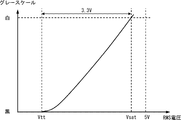
- FIG. 3 is a circuit diagram showing a specific configuration of an inverter constituting a first data holding unit provided in the pixel shown in FIG. 2. It is a schematic sectional drawing of the pixel shown in FIG. 2 is a timing chart illustrating an operation of the liquid crystal display device illustrated in FIG. 1. It is a figure which shows the relationship between the applied voltage (RMS voltage) of a liquid crystal, and the gray scale value of a liquid crystal.
- RMS voltage applied voltage
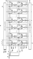
- FIG. 4 is a circuit diagram showing a specific configuration of a latch unit provided in the liquid crystal display device according to the concept prior to the first embodiment.
- FIG. FIG. 2 is a circuit diagram illustrating a specific configuration example of a latch unit provided in the liquid crystal display device illustrated in FIG. 1.
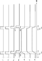
- 3 is a timing chart illustrating an operation of a latch unit provided in the liquid crystal display device illustrated in FIG. 1.
- FIG. 1 is a block diagram showing a liquid crystal display device 10 according to the first embodiment.
- the liquid crystal display device 10 includes an image display unit 11, a timing generator 13, a vertical shift register 14, a data latch circuit 15, and a horizontal driver 16.
- the horizontal driver 16 includes a horizontal shift register 161, a latch unit 162, and a level shifter / pixel driver 163.
- the image display unit 11 has a plurality of pixels 12 regularly arranged.
- the plurality of pixels 12 are connected to the vertical shift register 14 at one end and extend in the row direction (X direction) with m (m is a natural number of 2 or more) row scanning lines g1 to gm, and a level shifter / pixel driver 163.
- m is a natural number of 2 or more row scanning lines g1 to gm
- n column data lines d1 to dn a natural number of 2 or more
- All the pixels 12 in the image display unit 11 are commonly connected to trigger lines trig and trigb, one end of which is connected to the timing generator 13.
- the forward trigger pulse TRI transmitted by the forward trigger pulse trigger line trig and the inverted trigger pulse TRIB transmitted by the inverted trigger pulse trigger line trig are always in an inverse logical value relationship (complementary relationship). is there.
- the timing generator 13 receives external signals such as a vertical synchronization signal Vst, a horizontal synchronization signal Hst, and a basic clock CLK output from the host device 20 as input signals, and based on these external signals, AC signals FR, V Various internal signals such as a start pulse VST, an H start pulse HST, clock signals VCK and HCK, a latch pulse LT, and trigger pulses TRI and TRIB are generated.
- external signals such as a vertical synchronization signal Vst, a horizontal synchronization signal Hst, and a basic clock CLK output from the host device 20 as input signals, and based on these external signals, AC signals FR, V
- Various internal signals such as a start pulse VST, an H start pulse HST, clock signals VCK and HCK, a latch pulse LT, and trigger pulses TRI and TRIB are generated.
- the AC signal FR is a signal whose polarity is inverted every subframe, and is supplied to the common electrode of the liquid crystal display element in the pixel 12 constituting the image display unit 11 as a common electrode voltage Vcom described later.
- the start pulse VST is a pulse signal output at the start timing of each subframe described later, and switching of subframes is controlled by the start pulse VST.
- the start pulse HST is a pulse signal output to the horizontal shift register 161 at the start timing of the horizontal shift register 161.
- the clock signal VCK is a shift clock that defines one horizontal scanning period (1H) in the vertical shift register 14, and the vertical shift register 14 performs a shift operation at the timing of the clock signal VCK.
- the clock signal HCK is a shift clock in the horizontal shift register 161, and is a signal for shifting data with a 32-bit width.
- the latch pulse LT is a pulse signal that is output at a timing when the horizontal shift register 161 has finished shifting the data for the number of pixels in one row in the horizontal direction.
- the forward trigger pulse TRI and the inversion trigger pulse TRIB are pulse signals supplied to all the pixels 12 in the image display unit 11 via the trigger lines trig and trigb, respectively.
- the forward trigger pulse TRI and the inversion trigger pulse TRIB are output from the timing generator 13 after data is written in the first data holding units in all the pixels 12 in the image display unit 11 in a certain subframe period. Is done. Thereby, in the subframe period, the data held in the first data holding unit in all the pixels 12 in the image display unit 11 is transferred to the second data holding unit in the corresponding pixel 12 all at once.
- the vertical shift register 14 transfers the V start pulse VST supplied at the start timing of each subframe in accordance with the clock signal VCK, and sequentially supplies the row scanning signals to the row scanning lines g1 to gm sequentially in units of 1H. . Thereby, the row scanning lines are sequentially selected in units of 1H from the uppermost row scanning line g1 of the image display unit 11 to the lowermost row scanning line gm.
- the data latch circuit 15 latches 32-bit width data in units of one subframe supplied from an external circuit (not shown) based on the basic clock CLK from the host device 20, and then performs horizontal shift in synchronization with the basic clock CLK. Output to the register 161.
- the liquid crystal display device 10 divides one frame of the video signal into a plurality of subframes having a display period shorter than the one frame period of the video signal, and performs gradation display by combining these subframes. . Therefore, the external circuit converts the gradation data indicating the gradation of each pixel into a plurality of 1-bit subframe data corresponding to a plurality of subframes. Further, the external circuit collectively supplies the sub-frame data for 32 pixels belonging to the same sub-frame to the data latch circuit 15 as 32-bit width data.
- the horizontal shift register 161 When viewed as a 1-bit serial data processing system, the horizontal shift register 161 starts shifting by a start pulse HST supplied at the beginning of 1H from the timing generator 13, and 32-bit width data supplied from the data latch circuit 15. Are shifted in synchronization with the clock signal HCK.
- the latch unit 162 synchronizes with the latch pulse LT supplied from the timing generator 13
- Data of n bits (that is, subframe data of n pixels) supplied in parallel from the horizontal shift register 161 is latched and output to the level shifter of the level shifter / pixel driver 163.
- the start pulse HST is output again from the timing generator 13
- the horizontal shift register 161 resumes the 32-bit width data shift from the data latch circuit 15 in accordance with the clock signal HCK.
- the level shifter of the level shifter / pixel driver 163 shifts the signal level of n subframe data corresponding to n pixels in one row transferred from the latch unit 162 to the liquid crystal drive voltage amplitude.
- the pixel driver of the level shifter / pixel driver 163 outputs n pieces of subframe data corresponding to n pixels in one row after the level shift to n column data lines d1 to dn in parallel.
- the horizontal driver 16 outputs subframe data to pixels in a row selected as a data writing target in one horizontal scanning period, and outputs pixels in a row selected as a data writing target in the next one horizontal scanning period. Therefore, the subframe data is shifted in parallel. Then, in a certain horizontal scanning period, n subframe data corresponding to n pixels in one row are simultaneously output in parallel to the n column data lines d1 to dn as data signals.
- n pixels 12 in one row selected by the row scanning signal from the vertical shift register 14 are one row output from the level shifter / pixel driver 163 all at once.
- N subframe data are sampled via n column data lines d1 to dn and written in a first data holding unit (to be described later) in each pixel 12.
- the inverted data of the input data held in the storage unit SM1 is applied to the reflective electrode PE. That is, the pixel 12 has a function of inverting the input data supplied from the level shifter / pixel driver 163.
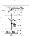
- FIG. 2 is a circuit diagram showing a specific configuration of the pixel 12.
- the pixel 12 has one of row scanning lines g1 to gm (hereinafter referred to as row scanning line g) and one of column data lines d1 to dn (hereinafter referred to as column data line d). ) And are provided at the intersection.
- the pixel 12 includes an SRAM cell 201, a DRAM cell 202, and a liquid crystal display element LC.
- the SRAM cell 201 includes a switch SW1 that is a first switch and a storage unit SM1 that is a first data holding unit.
- the DRAM cell 202 includes a switch SW2 that is a second switch and a storage unit DM2 that is a second data holding unit.
- the liquid crystal display element LC has a known structure in which a liquid crystal LCM is filled and enclosed in a space between a reflective electrode PE, which is a pixel electrode having light reflection characteristics arranged in a spaced-apart relationship, and a common electrode CE having light transmittance. It is.
- the switch SW1 is composed of, for example, an N-channel MOS transistor (hereinafter referred to as NMOS transistor) MN1.
- NMOS transistor MN1 N-channel MOS transistor
- the source is connected to the input terminal (node a) of the storage unit SM1
- the drain is connected to the column data line d
- the gate is connected to the row scanning line g.
- the storage unit SM1 is a self-holding memory composed of two inverters INV11 and INV12 having one output terminal connected to the other input terminal. More specifically, the input terminal of the inverter INV11 is connected to the output terminal of the inverter INV12 and the source of the NMOS transistor MN1 constituting the switch SW1. The input terminal of the inverter INV12 is connected to the switch SW2 and the output terminal of the inverter INV11.
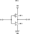
- FIG. 3 is a circuit diagram showing a specific configuration of the inverter INV11.
- the inverter INV11 has a P-channel MOS transistor (hereinafter referred to as PMOS transistor) MP11 and an NMOS transistor MN11 connected in series, and inverts the input signals supplied to the respective gates.
- PMOS transistor P-channel MOS transistor
- MN11 NMOS transistor
- This is a well-known CMOS inverter that outputs from the drain of each of them.
- the inverter INV12 has a PMOS transistor MP12 and an NMOS transistor MN12 connected in series, and is a known CMOS inverter that inverts an input signal supplied to each gate and outputs it from each drain.
- the driving capabilities of the inverters INV11 and INV12 are different. Specifically, out of the inverters INV11 and INV12 constituting the storage unit SM1, the drive capability of the transistors MP11 and MN11 in the inverter INV11 on the input side when viewed from the switch SW1 is the inverter on the output side when viewed from the switch SW1. It is larger than the drive capability of the transistors MP12 and MN12 in the INV12. As a result, data easily propagates from the column data line d to the storage unit SM1 via the switch SW1, while data does not easily propagate from the storage unit DM2 to the storage unit SM1 via the switch SW2.
- the driving capability of the NMOS transistor MN1 constituting the switch SW1 is larger than the driving capability of the NMOS transistor MN12 constituting the inverter INV12. Accordingly, for example, when data indicating the H level on the column data line d is stored in the storage unit SM1, the current flowing from the column data line d to the input terminal (node a) of the storage unit SM1 via the switch SW1 is: Since the current flows from the input terminal of the storage unit SM1 to the ground voltage terminal GND via the NMOS transistor MN12, the data can be accurately stored in the storage unit SM1.
- the switch SW2 is a known transmission gate including an NMOS transistor MN2 and a PMOS transistor MP2 connected in parallel. More specifically, in the NMOS transistor MN2 and the PMOS transistor MP2, each source is commonly connected to the output terminal of the storage unit SM1, and each drain is connected to the input terminal of the storage unit DM2 and the reflective electrode PE of the liquid crystal display element LC. Commonly connected.
- the gate of the NMOS transistor MN2 is connected to the normal trigger pulse trigger line trig, and the gate of the PMOS transistor MP2 is connected to the inverted trigger pulse trigger line trigger.
- the switch SW2 is turned on when the normal rotation trigger pulse supplied via the trigger line trig is H level (the reverse trigger pulse supplied via the trigger line trigb is L level), and the switch SW2 is turned on.
- the read data is transferred to the storage unit DM2 and the reflective electrode PE.
- the switch SW2 is turned off when the normal rotation trigger pulse supplied via the trigger line trig is L level (the reverse trigger pulse supplied via the trigger line trigb is H level), and the switch SW2 The stored data is not read.
- the switch SW2 Since the switch SW2 is a known transmission gate, it can transfer a wide range of voltages from the ground voltage GND to the power supply voltage VDD in the on state. More specifically, when the voltage applied from the storage unit SM1 to the sources of the transistors MN2 and MP2 is the ground voltage GND level (L level), the source / drain of the PMOS transistor MP2 is not conducted, but the NMOS transistor MN2 The source / drain can be conducted with low resistance. On the other hand, when the voltage applied from the storage unit SM1 to the sources of the transistors MN2 and MP2 is the power supply voltage VDD level (H level), the source and drain of the PMOS transistor MP2 are It can conduct with low resistance. As described above, in the switch SW2, since the source and drain of the transmission gate can be conducted with low resistance, a wide range of voltages from the ground voltage GND to the power supply voltage VDD can be transferred in the on state.
- the storage unit DM2 is configured by a capacity C1.
- the capacitor C1 include a MIM (Metal Insulator Metal) capacitor that forms a capacitor between wirings, a Diffusion capacitor that forms a capacitor between a substrate and polysilicon, or a PIP (Poly) that forms a capacitor between two layers of polysilicon. Insulator Poly) capacity or the like can be used.
- the switch SW2 When the switch SW2 is turned on, the data stored in the storage unit SM1 is read and transferred to the capacitor C1 and the reflection electrode PE in the storage unit DM2 via the switch SW2. Thereby, the data stored in the storage unit DM2 is rewritten.
- the data held in the capacitor C1 also affects the input gate of the inverter INV12 constituting the storage unit SM1.
- the inverter INV11 since the drive capability of the inverter INV11 is larger than the drive capability of the inverter INV12, the inverter INV11 rewrites the data of the capacitor C1 before the inverter INV12 is affected by the data of the capacitor C1. Therefore, the data stored in the storage unit SM1 is not unintentionally rewritten by the data held in the capacitor C1.
- the liquid crystal display device 10 uses the pixel 12 including one SRAM cell and one DRAM cell, so that the pixel is more effective than the case where the pixel including two SRAM cells is used. By reducing the number of transistors that are configured, the size of the pixel is reduced.
- the switch SW2 includes the PMOS transistor MP2 and the NMOS transistor MN2 has been described, but the present invention is not limited to this.
- the switch SW2 can be appropriately changed to a configuration in which any one of the PMOS transistor MP2 and the NMOS transistor MN2 is provided. In that case, only one of the trigger lines trig, trigb is provided.
- the liquid crystal display device 10 can not only reduce the size of the pixel by reducing the number of transistors constituting the pixel, but also store the storage units SM1 and DM2 and the reflection electrode PE as described below. It is also possible to reduce the size of the pixels by arranging them effectively in the direction. Hereinafter, it demonstrates in detail using FIG.
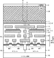
- FIG. 4 is a schematic cross-sectional view showing the main part of the pixel 12.
- FIG. 4 illustrates an example in which the capacitor C1 is configured by an MIM that forms a capacitor between wirings.
- an N well 101 and a P well 102 are formed on a silicon substrate 100.
- the PMOS transistor MP2 of the switch SW2 and the PMOS transistor MP11 of the inverter INV11 are formed on the N well 101. More specifically, a common diffusion layer serving as the source of each of the PMOS transistors MP2 and MP11 and two diffusion layers serving as the drain are formed on the N well 101, and the common diffusion layer, the two diffusion layers, Polysilicon serving as the gates of the PMOS transistors MP2 and MP11 is formed on the channel region between the two through a gate oxide film.
- an NMOS transistor MN2 of the switch SW2 and an NMOS transistor MN11 of the inverter INV11 are formed on the P well 102. More specifically, a common diffusion layer serving as the source of each of the NMOS transistors MN2 and MN11 and two diffusion layers serving as the drain are formed on the P well 102, and the common diffusion layer, the two diffusion layers, Polysilicon serving as the gates of the NMOS transistors MN2 and MN11 is formed on the channel region between the two through a gate oxide film.
- An element isolation oxide film 103 is formed between the active region (diffusion layer and channel region) on the N well and the active region on the P well.
- an interlayer insulating film 105 is interposed between the metals, the first metal 106, the second metal 108, the third metal 110, the MIM electrode 112, the fourth metal 114, and A fifth metal 116 is laminated.
- the fifth metal 116 constitutes a reflective electrode PE formed for each pixel.
- Each diffusion layer that constitutes each drain of the transistors MN2 and MP2 includes a contact 118, a first metal 106, a through hole 119a, a second metal 108, a through hole 119b, a third metal 110, a through hole 119c, a fourth metal 114, And, it is electrically connected to the fifth metal 116 through the through hole 119e. Further, each diffusion layer constituting each drain of the transistors MN2 and MP2 includes a contact 118, a first metal 106, a through hole 119a, a second metal 108, a through hole 119b, a third metal 110, a through hole 119c, and a fourth metal. 114 and the through hole 119d are electrically connected to the MIM electrode 112. That is, the sources of the transistors MN2 and MP2 constituting the switch SW2 are electrically connected to the reflective electrode PE and the MIM electrode 112.
- the reflective electrode PE (fifth metal 116) is disposed so as to be opposed to the common electrode CE, which is a transparent electrode, via a passivation film (PSV) 117, which is a protective film formed on the upper surface thereof.
- a liquid crystal LCM is filled and sealed between the reflective electrode PE and the common electrode CE.
- a liquid crystal display element LC is configured by the reflective electrode PE, the common electrode CE, and the liquid crystal LCM therebetween.
- the MIM electrode 112 is formed on the third metal 110 via the interlayer insulating film 105.
- the MIM electrode 112, the third metal 110, and the interlayer insulating film 105 between them constitute a capacitor C1. Therefore, the switches SW1 and SW2 and the storage unit SM1 are formed using the first metal 106 and the second metal 108, which are the first and second layer wirings, and the transistor, whereas the storage unit DM2 It is formed using the third metal 110 and the MIM electrode 112 which are upper layers. That is, the switches SW1 and SW2, the storage unit SM1, and the storage unit DM2 are formed in different layers.
- Light from a light source passes through the common electrode CE and the liquid crystal LCM, is incident on the reflective electrode PE (fifth metal 116), is reflected, and travels backward through the original incident path and is emitted through the common electrode CE. .
- the liquid crystal display device 10 uses the fifth metal 116 that is the fifth layer wiring as the reflective electrode PE, the third metal 110 that is the third layer wiring as a part of the memory unit DM2,
- the first metal 106 and the second metal 108 which are two-layer wiring, and the transistor as the memory unit SM1, etc.
- the pixel can be further reduced in size.
- pixels with a pitch of 3 ⁇ m or less can be configured with transistors having a power supply voltage of 3.3V.
- a liquid crystal display panel having a diagonal length of 0.55 inches and a horizontal direction of 4000 pixels and a vertical direction of 2000 pixels can be realized.
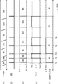
- FIG. 5 is a timing chart showing the operation of the liquid crystal display device 10.
- the row scanning lines g 1 to gm are sequentially selected in units of 1H by the row scanning signal from the vertical shift register 14. Data is written to each pixel 12 in units of n pixels in one row commonly connected to the selected row scanning line. Then, when data is written in all of the plurality of pixels 12 constituting the image display unit 11, thereafter, the data of all the pixels 12 are simultaneously read based on the trigger pulses TRI and TRIB (more specifically, Data in the storage unit SM1 in all the pixels 12 is transferred to the storage unit DM2 and the reflective electrode PE all at once).
- FIG. 5 shows changes in subframe data stored in each pixel 12.
- the vertical axis represents the row number, and the horizontal axis represents time.
- the boundary line of the subframe data has a lower right side. This indicates that the sub-frame data is written later as the pixel having a larger row number.
- a period from one end to the other end of the boundary line corresponds to a subframe data writing period.
- B0b, B1b, and B2b indicate inverted data of subframe data of bits B0, B1, and B2, respectively.
- FIG. 5B shows the output timing (rise timing) of the trigger pulse TRI.
- the trigger pulse TRIB is omitted because it always indicates a logically inverted value of the trigger pulse TRI.
- FIG. 5C schematically shows the bits of the subframe data applied to the reflective electrode PE.
- FIG. 5D shows a change in the value of the common electrode voltage Vcom.
- FIG. 5E shows a change in voltage applied to the liquid crystal LCM.
- the switch SW1 is turned on, so that the normal subframe data of the bit B0 output from the horizontal driver 16 to the column data line d is sampled by the switch SW1 and stored in the storage unit.
- SM1 normal rotation subframe data of bit B0 is written in the storage unit SM1 of all the pixels 12 constituting the image display unit 11.
- the H level trigger pulse TRI and the L level trigger pulse TRIB is simultaneously supplied to all the pixels 12 constituting the image display unit 11 (time T1).
- the switches SW2 of all the pixels 12 are turned on, so that the normal subframe data of the bit B0 stored in the storage unit SM1 is transferred to the storage unit DM2 all at once through the switch SW2 and held.
- B0 normal rotation subframe data is applied to the reflective electrode PE.
- the retention period of the normal subframe data of bit B0 by the storage unit DM2 (application period of the normal subframe data of bit B0 to the reflective electrode PE). Is one subframe period from the time when the trigger pulse TRI becomes H level (time T1) to the time when it again becomes H level (time T2).
- the power supply voltage VDD (3.3 V in this case) is applied to the reflective electrode PE
- the bit value is “0”, that is, L level.
- a ground voltage GND (0 V) is applied to the reflective electrode PE.
- a free voltage can be applied to the common electrode CE as the common electrode voltage Vcom without being limited to the ground voltage GND and the power supply voltage VDD.
- the common electrode voltage Vcom is controlled to be switched to a predetermined voltage in synchronization.
- the common electrode voltage Vcom is equal to the threshold voltage Vtt of the liquid crystal rather than 0V, as shown in FIG. 5D, during the subframe period in which the normal subframe data of bit B0 is applied to the reflective electrode PE. Set to low voltage.
- FIG. 6 shows the relationship between the applied voltage (RMS voltage) of the liquid crystal and the gray scale value of the liquid crystal.
- the storage unit SM1 of all the pixels 12 constituting the image display unit 11 is stored. Writing of the inverted subframe data of bit B0 is sequentially started. When the inverted subframe data of bit B0 is written to the storage unit SM1 of all the pixels 12 constituting the image display unit 11, the H level is then applied to all the pixels 12 constituting the image display unit 11. Trigger pulse TRI (and L level trigger pulse TRIB) are simultaneously supplied (time T2).
- the switches SW2 of all the pixels 12 are turned on, so that the inverted subframe data of the bit B0 stored in the storage unit SM1 is simultaneously transferred to and held in the storage unit DM2 through the switch SW2, and the bit B0
- the inverted subframe data is applied to the reflective electrode PE.
- the retention period of the inverted subframe data of bit B0 by the storage unit DM2 is as follows. This is one subframe period from the time when the trigger pulse TRI becomes H level (time T2) to the time when it again becomes H level (time T3).
- the inverted subframe data of bit B0 is always in an inverse logical value relationship with the normal subframe data of bit B0, when the normal subframe data of bit B0 is “1”, “0” When the normal rotation subframe data of B0 is “0”, it is “1”.
- the common electrode voltage Vcom is higher than the 3.3V threshold voltage Vtt as shown in FIG. 5D during the subframe period in which the inverted subframe data of the bit B0 is applied to the reflective electrode PE.
- the bit value of the normal subframe data of bit B0 is “1”
- the bit value of the inverted subframe data of bit B0 applied subsequently is “0”.
- the applied voltage of the liquid crystal LCM is ⁇ (3.3V + Vtt), and the potential direction is reversed but the absolute value is the same as compared to when the normal rotation subframe data of the bit B0 is applied. . Therefore, the pixel 12 displays white when the inverted subframe data of the bit B0 is applied, similarly to when the normal frame data of the bit B0 is applied.
- the bit value of the normal subframe data of bit B0 is “0”
- the bit value of the inverted subframe data of bit B0 applied subsequently is “1”.
- the voltage applied to the liquid crystal LCM is ⁇ Vtt, and the potential direction is reversed but the absolute value is the same as when the normal subframe data of the bit B0 is applied. Therefore, the pixel 12 displays black when the inverted subframe data of the bit B0 is applied, similarly to when the normal frame data of the bit B0 is applied.
- the pixel 12 displays the same gradation in the bit B0 and the complementary bit B0b of the bit B0 during the two subframe periods from time T1 to time T3, and the liquid crystal LCM Since AC driving in which the potential direction is reversed for each subframe is performed, burn-in of the liquid crystal LCM can be prevented.
- the normal subframe data of bit B1 is written to the storage unit SM1 of all the pixels 12.
- the H level trigger is then applied to all the pixels 12 constituting the image display unit 11.
- the pulse TRI (and the L level trigger pulse TRIB) is simultaneously supplied (time T3).
- the switches SW2 of all the pixels 12 are turned on, so that the normal subframe data of the bit B1 stored in the storage unit SM1 is transferred to the storage unit DM2 all at once through the switch SW2, and held.
- the normal rotation subframe data of bit B1 is applied to the reflective electrode PE.
- the retention period of the normal subframe data of bit B1 by the storage unit DM2 Is one subframe period from the time when the trigger pulse TRI becomes H level (time T3) to the time when it again becomes H level (time T4).
- the switches SW2 of all the pixels 12 are turned on, so that the inverted subframe data of the bit B1 stored in the storage unit SM1 is transferred and held all at once to the storage unit DM2 through the switch SW2, and the bit B1
- the inverted subframe data is applied to the reflective electrode PE.
- the retention period of the inverted subframe data of the bit B1 by the storage unit DM2 is: This is one subframe period from when the trigger pulse TRI becomes H level (time T4) until it becomes H level again (time T5).
- the inverted subframe data of bit B1 is always in the relationship of the inverse logical value with the normal subframe data of bit B1.
- the common electrode voltage Vcom is higher than the 3.3V threshold voltage Vtt as shown in FIG. 5D during the subframe period in which the inverted subframe data of the bit B1 is applied to the reflective electrode PE.
- the pixel 12 displays the same gradation in the bit B1 and the complementary bit B1b of the bit B1 and the liquid crystal LCM during the two subframes from time T3 to T5. Since the alternating current driving in which the potential direction is inverted every subframe, the burn-in of the liquid crystal LCM can be prevented. The same operation is repeated for bits B2 and thereafter.
- the liquid crystal display device 10 performs gradation display using a combination of a plurality of subframes.
- the display periods of bit B0 and complementary bit B0b are the same first subframe period, and the display periods of bit B1 and complementary bit B1b are also the same second subframe period.
- the subframe period and the second subframe period are not necessarily the same.
- the second subframe period is set to be twice the first subframe period.
- the third subframe period which is the display period of the bit B2 and the complementary bit B2b, is set to be twice the second subframe period. The same can be said for other subframe periods.
- the length of each subframe period and the number of subframes can be arbitrarily set according to the system specifications and the like.
- FIG. 7 is a circuit diagram showing a specific configuration of the latch unit 562 according to the concept before reaching the first embodiment. 7 also shows a horizontal shift register 161 and a level shifter / pixel driver 163 which are peripheral circuits of the latch unit 562.
- the latch unit 562 includes n latch circuits 564 corresponding to n columns of the plurality of pixels 12 arranged in a matrix.
- Each of the n latch circuits 564 is disposed opposite to the n pixels 12 arranged in the row direction, and has a pitch (width in the row direction) corresponding to the pitch of the n pixels 12. Yes.
- the latch unit 562 is supplied with pulse signals P1, P1b, P2, and P2b obtained by normalizing or inverting the latch pulse LT from the timing generator 13. More specifically, the latch unit 562 is supplied with pulse signals P1 and P2b obtained by normalizing the latch pulse LT by the buffer BF1, and pulse signals P1b and P2 obtained by inverting the latch pulse LT by the inverter IV1. Supplied.
- the switch SW21 is a known transmission gate including an NMOS transistor MN21 and a PMOS transistor MP21 connected in parallel. More specifically, in the NMOS transistor MN21 and the PMOS transistor MP21, each source is commonly connected to a corresponding output terminal in the horizontal shift register 161, and each drain is commonly connected to an input terminal of the inverter IV21.
- a pulse signal P1 is supplied to the gate of the NMOS transistor MN21, and a pulse signal P1b that is an inverted signal of the pulse signal P1 is supplied to the gate of the PMOS transistor MP21.
- the output terminal of the inverter IV21 is connected to the input terminal of the inverter IV22 and the corresponding input terminal of the level shifter / pixel driver 163.
- the switch SW22 is a known transmission gate including an NMOS transistor MN22 and a PMOS transistor MP22 connected in parallel. More specifically, in the NMOS transistor MN22 and the PMOS transistor MP22, the respective sources are commonly connected to the output terminal of the inverter IV22, and the respective drains are commonly connected to the input terminal of the inverter IV21.
- a pulse signal P2 is supplied to the gate of the NMOS transistor MN22, and a pulse signal P2b that is an inverted signal of the pulse signal P2 is supplied to the gate of the PMOS transistor MP22.
- the pulse signals P1 and P2b indicate the L level and the pulse signals P1b and P2 indicate the H level, so that the switch SW21 is turned off and the switch SW22 is turned on.
- the pulse signals P1 and P2b indicate the H level and the pulse signals P1b and P2 indicate the L level, so that the switch SW21 is turned on and the switch SW22 is turned off.
- the latch pulse LT indicates the L level. Accordingly, since the pulse signals P1 and P2b indicate the L level and the pulse signals P1b and P2 indicate the H level, the switch SW21 is turned off and the switch SW22 is turned on.
- the horizontal shift register 161 starts shifting by the start pulse HST supplied from the timing generator 13 at the beginning of 1H, and is supplied from the data latch circuit 15 as 32 bits. The width data is shifted in synchronization with the clock signal HCK.
- the latch pulse LT rises (switches from L level to H level).
- the pulse signals P1 and P2b rise (switch from L level to H level) and the pulse signals P1b and P2 fall (switch from H level to L level), so the switch SW21 is turned on and the switch SW22 is turned off.
- n-bit data that is, sub-frame data for n pixels
- the level shifter of the level shifter / pixel driver 163 shifts the signal level of n subframe data corresponding to n pixels in one row transferred from the latch unit 562 to the liquid crystal drive voltage amplitude.
- the pixel driver of the level shifter / pixel driver 163 outputs n subframe data corresponding to n pixels in one row after the level shift to n column data lines d1 to dn in parallel. That is, in a certain horizontal scanning period, n subframe data corresponding to n pixels in one row are simultaneously output in parallel to n column data lines d1 to dn as data signals.
- the latch pulse LT falls. Accordingly, the pulse signals P1 and P2b fall and the pulse signals P1b and P2 rise, so that the switch SW21 is turned off and the switch SW22 is turned on. Accordingly, the latch unit 562 is disconnected from the horizontal shift register 161, but continues to hold the sub-frame data for n pixels supplied from the horizontal shift register 161 until immediately before. Therefore, the latch unit 562 can continue to output the sub-frame data for the n pixels in parallel to the n column data lines d1 to dn.
- next 1H start pulse HST is supplied from the timing generator 13 to the horizontal shift register 161 during the period when the latch pulse LT is at the L level. Accordingly, the horizontal shift register 161 resumes the operation of shifting the 32-bit width data supplied from the data latch circuit 15.
- the horizontal driver 56 outputs the subframe data toward the pixel of the row selected as the data writing target in one horizontal scanning period and the pixel of the row selected as the data writing target in the next horizontal scanning period.
- the subframe data is shifted in parallel with the above.
- n sub-frame data directed to the n pixels 12 are parallel and simultaneously to the n column data lines d1 to dn in synchronization with the rising edge of the latch pulse LT. Is output. Accordingly, in the liquid crystal display device equipped with the latch unit 562, the current flowing from the power supply voltage terminal to the ground voltage terminal increases momentarily (that is, the peak current consumption increases), and thus the power supply voltage VDD decreases. There is a problem that an IR drop phenomenon occurs in which the ground voltage GND increases. As a result, in the liquid crystal display device equipped with the latch unit 562, for example, a malfunction may occur or the image quality may deteriorate.
- the latch unit 162 and the liquid crystal display device 10 equipped with the latch unit 162 have been found so that the IR drop can be prevented by suppressing the peak current consumption.
- FIG. 8 is a circuit diagram illustrating a specific configuration example of the latch unit 162 according to the first embodiment. 8 also shows a horizontal shift register 161 and a level shifter / pixel driver 163, which are peripheral circuits of the latch unit 162.
- the latch unit 162 includes n latch circuits 164 provided corresponding to n columns of the plurality of pixels 12 arranged in a matrix.
- Each of the n latch circuits 164 is arranged to face the n pixels 12 arranged in the row direction, and has a pitch (width in the row direction) corresponding to the pitch of the n pixels 12. Yes.
- the latch unit 162 includes delay buffers D1L, D1bL, D2L, D2bL, and delay buffers D1R, D1bR, D2R, D2bR. These delay buffers serve as a timing adjustment circuit that adjusts the supply timing of subframe data to each of the n pixels 12 provided in each row of the plurality of pixels 12. Details will be described later.
- n latch circuits 164 are divided into a plurality of latch circuit groups.
- n latch circuits 164 include n / 3 latch circuits 164 (latch circuit group 1642) arranged in the center, and the negative side in the row direction (left side of the drawing) than latch circuit group 1642.
- N / 3 latch circuits 164 (latch circuit group 1641) arranged in the n, and n / 3 latch circuits 164 (latch circuits) arranged on the positive side in the row direction (right side of the drawing) from the latch circuit group 1642 Group 1643).
- the latch circuit group 1642 provided in the center of the latch unit 162 is supplied with pulse signals P1, P1b, P2, and P2b obtained by normal rotation or inversion of the latch pulse LT from the timing generator 13. More specifically, the latch circuit group 1642 is supplied with pulse signals P1 and P2b obtained by normalizing the latch pulse LT by the buffer BF1, and pulse signals P1b and P2 obtained by inverting the latch pulse LT by the inverter IV1. Is supplied.
- the latch circuit group 1641 provided in the left region of the latch unit 162 includes pulse signals P1L, P1bL obtained by delaying the pulse signals P1, P1b, P2, P2b using delay buffers D1L, D1bL, D2L, D2bL, respectively. , P2L, P2bL are supplied.
- the latch circuit group 1643 provided in the right region of the latch unit 162 includes pulse signals P1R, P1bR obtained by delaying the pulse signals P1, P1b, P2, P2b using the delay buffers D1R, D1bR, D2R, D2bR, respectively. , P2R, P2bR are supplied.
- the switch SW21 is a known transmission gate including an NMOS transistor MN21 and a PMOS transistor MP21 connected in parallel. More specifically, in the NMOS transistor MN21 and the PMOS transistor MP21, each source is commonly connected to a corresponding output terminal in the horizontal shift register 161, and each drain is commonly connected to an input terminal of the inverter IV21.
- a pulse signal P1 is supplied to the gate of the NMOS transistor MN21, and a pulse signal P1b that is an inverted signal of the pulse signal P1 is supplied to the gate of the PMOS transistor MP21.
- the output terminal of the inverter IV21 is connected to the input terminal of the inverter IV22 and the corresponding input terminal of the level shifter / pixel driver 163.
- the switch SW22 is a known transmission gate including an NMOS transistor MN22 and a PMOS transistor MP22 connected in parallel. More specifically, in the NMOS transistor MN22 and the PMOS transistor MP22, the respective sources are commonly connected to the output terminal of the inverter IV22, and the respective drains are commonly connected to the input terminal of the inverter IV21.
- a pulse signal P2 is supplied to the gate of the NMOS transistor MN22, and a pulse signal P2b that is an inverted signal of the pulse signal P2 is supplied to the gate of the PMOS transistor MP22.
- the switch SW21 is turned off and the switch SW22 is turned on.
- the pulse signals P1 and P2b indicate the H level
- the pulse signals P1b and P2 indicate the L level.
- each latch circuit 164 of the latch circuit group 1641 provided in the left region of the latch unit 162 the pulse signal P1L is supplied to the gate of the NMOS transistor MN21, and the inverted signal of the pulse signal P1L is supplied to the gate of the PMOS transistor MP21.
- the pulse signal P1bL is supplied.
- a pulse signal P2L is supplied to the gate of the NMOS transistor MN22, and a pulse signal P2bL that is an inverted signal of the pulse signal P2L is supplied to the gate of the PMOS transistor MP22.
- the other configuration of each latch circuit 164 in the latch circuit group 1641 is the same as the configuration of each latch circuit 164 in the latch circuit group 1642, and thus description thereof is omitted.
- the pulse signals P1, P2b indicate the L level
- the pulse signals P1b, P2 indicate the H level
- the pulse signals P1L, P2bL are L level is indicated
- the pulse signals P1bL and P2L indicate H level. Accordingly, in each latch circuit 164 of the latch circuit group 1641, the switch SW21 is turned off and the switch SW22 is turned on.
- the pulse signals P1 and P2b indicate the H level
- the pulse signals P1b and P2 indicate the L level
- the pulse signals P1L and P2bL are The H level is indicated
- the pulse signals P1bL and P2L indicate the L level. Accordingly, in each latch circuit 164 of the latch circuit group 1641, the switch SW21 is turned on and the switch SW22 is turned off.
- each latch circuit 164 of the latch circuit group 1643 provided in the right region of the latch unit 162, the pulse signal P1R is supplied to the gate of the NMOS transistor MN21, and the inverted signal of the pulse signal P1R is supplied to the gate of the PMOS transistor MP21.
- a pulse signal P1bR is supplied.
- the pulse signal P2R is supplied to the gate of the NMOS transistor MN22, and the pulse signal P2bR that is an inverted signal of the pulse signal P2R is supplied to the gate of the PMOS transistor MP22.
- the other configuration of each latch circuit 164 in the latch circuit group 1643 is the same as the configuration of each latch circuit 164 in the latch circuit group 1642, and thus description thereof is omitted.
- the pulse signals P1 and P2b indicate the L level
- the pulse signals P1b and P2 indicate the H level
- the pulse signals P1R and P2bR are The L level is indicated
- the pulse signals P1bR and P2R indicate the H level. Accordingly, in each latch circuit 164 of the latch circuit group 1643, the switch SW21 is turned off and the switch SW22 is turned on.
- the pulse signals P1 and P2b indicate the H level
- the pulse signals P1b and P2 indicate the L level
- the pulse signals P1R and P2bR are The H level is indicated
- the pulse signals P1bR and P2R indicate the L level. Accordingly, in each latch circuit 164 of the latch circuit group 1643, the switch SW21 is turned on and the switch SW22 is turned off.
- signal lines through which the pulse signals P1, P1b, P2, and P2b propagate are mainly wired to a wiring layer (for example, an upper wiring layer) different from the wiring layer that constitutes the latch circuit 164.
- the signal line through which the pulse signals P1L, P1bL, P2L, and P2bL propagate and the signal line through which the pulse signals P1R, P1bR, P2R, and P2bR propagate are mainly different from the wiring layers that constitute the latch circuit 164. It is partially disposed on a wiring layer (for example, an upper wiring layer).
- the delay buffers D1L, D1bL, D2L, D2bL and the delay buffers D1R, D1bR, D2R, D2bR are all formed in a region different from the region constituting the latch circuit 164 (for example, the upper side in FIG. 8).
- the n latch circuits 164 can be arranged to face the n pixels 12 arranged in the row direction without being affected by the delay buffer and without disturbing the pitch. Thereby, the liquid crystal display device 10 can display the entire image displayed on the image display unit 11 uniformly.
- the delay buffer is arranged in a different area from the latch circuit 164, the size and the number of stages can be changed with a high degree of freedom.
- FIG. 9 is a timing chart showing the operation of the latch unit 162.
- FIG. 9 shows an example in which “1” is written to the n pixels 12 in the first row and “0” is written to the n pixels 12 in the second row.
- the latch pulse LT indicates the L level (time T0). Accordingly, since the pulse signals P1 and P2b indicate the L level and the pulse signals P1b and P2 indicate the H level, in each latch circuit 164 of the latch circuit group 1642, the switch SW21 is turned off and the switch SW22 is turned on. . Further, since the pulse signals P1L and P2bL indicate the L level and the pulse signals P1bL and P2L indicate the H level, in each latch circuit 164 of the latch circuit group 1641, the switch SW21 is turned off and the switch SW22 is turned on. Further, since the pulse signals P1R and P2bR indicate L level and the pulse signals P1bR and P2R indicate H level, in each latch circuit 164 of the latch circuit group 1643, the switch SW21 is turned off and the switch SW22 is turned on.
- the level shifter of the level shifter / pixel driver 163 shifts the level of the n / 3 subframe data transferred from the latch unit 162 to the liquid crystal drive voltage amplitude.
- the pixel driver of the level shifter / pixel driver 163 converts the n / 3 subframe data after the level shift into n / 3 column data lines d () corresponding to the latch circuits 164 of the latch circuit group 1642.
- the data is output in parallel to the column data line group dM). Thereby, the voltage level of each column data line d of the column data line group dM is switched from the L level to the H level (time T11).
- the pulse signals P1 and P2b rise and the pulse signals P1b and P2 fall the pulse signals P1L and P2bL rise and the pulse signals P1bL and P2L fall after a predetermined delay time (time T12). Accordingly, in each latch circuit 164 of the latch circuit group 1641, the switch SW21 is turned on and the switch SW22 is turned off. Accordingly, n / 3 subframe data corresponding to each latch circuit 164 of the latch circuit group 1641 out of the subframe data for n pixels in the first row output from the horizontal shift register 161 is converted into level shifters / pixels. It is transferred to the driver 163.
- the level shifter of the level shifter / pixel driver 163 shifts the level of the n / 3 subframe data transferred from the latch unit 162 to the liquid crystal drive voltage amplitude.
- the pixel driver of the level shifter / pixel driver 163 converts the n / 3 subframe data after the level shift into n / 3 column data lines d () corresponding to the latch circuits 164 of the latch circuit group 1641.
- the data is output in parallel to the column data line group dL).
- the voltage level of each column data line d in the column data line group dL is switched from the L level to the H level (time T12).
- FIG. 9 shows a case where the delay buffers D1R, D1bR, D2R, D2bR in FIG. 8 are delayed from the delay buffers D1L, D1bL, D2L, D2bL. This is because the peak current consumption is reduced by reducing the number of circuits operating at one time by making the left and right delay times different.
- the delay buffers D1R, D1bR, D2R, and D2bR can be set to the same delay time as the delay buffers D1L, D1bL, D2L, and D2bL. Accordingly, in each latch circuit 164 of the latch circuit group 1643, the switch SW21 is turned on and the switch SW22 is turned off. Accordingly, n / 3 subframe data corresponding to each latch circuit 164 of the latch circuit group 1643 among the subframe data for n pixels in the first row output from the horizontal shift register 161 is converted into level shifters / pixels. It is transferred to the driver 163.
- the level shifter of the level shifter / pixel driver 163 shifts the level of the n / 3 subframe data transferred from the latch unit 162 to the liquid crystal drive voltage amplitude.
- the pixel driver of the level shifter / pixel driver 163 converts the n / 3 subframe data after the level shift into n / 3 column data lines d (provided corresponding to the latch circuits 164 of the latch circuit group 1643).
- the data is output in parallel to the column data line group dR).
- the voltage level of each column data line d in the column data line group dR is switched from the L level to the H level (time T13).
- the latch pulse LT falls (time T14).
- the latch unit 162 is disconnected from the horizontal shift register 161, but continues to hold the sub-frame data for n pixels supplied from the horizontal shift register 161 until immediately before. Therefore, the latch unit 162 can continue to output the sub-frame data for the n pixels in parallel to the n column data lines d1 to dn. As a result, the voltage levels of the n column data lines d1 to dn are maintained at the H level.
- the level shifter of the level shifter / pixel driver 163 shifts the level of the n / 3 subframe data transferred from the latch unit 162 to the liquid crystal drive voltage amplitude.
- the pixel driver of the level shifter / pixel driver 163 converts the n / 3 subframe data after the level shift into n / 3 column data lines d () corresponding to the latch circuits 164 of the latch circuit group 1642.
- the data is output in parallel to the column data line group dM). Thereby, the voltage level of each column data line d in the column data line group dM is switched from the H level to the L level (time T21).
- the pulse signals P1 and P2b rise and the pulse signals P1b and P2 fall the pulse signals P1L and P2bL rise and the pulse signals P1bL and P2L fall after a predetermined delay time (time T22). Accordingly, in each latch circuit 164 of the latch circuit group 1641, the switch SW21 is turned on and the switch SW22 is turned off. Accordingly, n / 3 subframe data corresponding to each latch circuit 164 of the latch circuit group 1641 out of the subframe data for n pixels in the second row output from the horizontal shift register 161 is converted into level shifters / pixels. It is transferred to the driver 163.
- the level shifter of the level shifter / pixel driver 163 shifts the level of the n / 3 subframe data transferred from the latch unit 162 to the liquid crystal drive voltage amplitude.
- the pixel driver of the level shifter / pixel driver 163 converts the n / 3 subframe data after the level shift into n / 3 column data lines d () corresponding to the latch circuits 164 of the latch circuit group 1641.
- the data is output in parallel to the column data line group dL). Thereby, the voltage level of each column data line d of the column data line group dL is switched from the H level to the L level (time T22).
- the pulse signals P1 and P2b rise and the pulse signals P1b and P2 fall the pulse signals P1R and P2bR rise and the pulse signals P1bR and P2R fall after a predetermined delay time (time T23). Accordingly, in each latch circuit 164 of the latch circuit group 1643, the switch SW21 is turned on and the switch SW22 is turned off. Accordingly, n / 3 subframe data corresponding to each latch circuit 164 of the latch circuit group 1643 out of the subframe data for n pixels in the second row output from the horizontal shift register 161 is converted into level shifters / pixels. It is transferred to the driver 163.
- the level shifter of the level shifter / pixel driver 163 shifts the level of the n / 3 subframe data transferred from the latch unit 162 to the liquid crystal drive voltage amplitude.
- the pixel driver of the level shifter / pixel driver 163 converts the n / 3 subframe data after the level shift into n / 3 column data lines d (provided corresponding to the latch circuits 164 of the latch circuit group 1643).
- the data is output in parallel to the column data line group dR). Thereby, the voltage level of each column data line d in the column data line group dR is switched from the H level to the L level (time T23).
- the latch pulse LT falls (time T24).
- the latch unit 162 is disconnected from the horizontal shift register 161, but continues to hold the sub-frame data for n pixels supplied from the horizontal shift register 161 until immediately before. Therefore, the latch unit 162 can continue to output the sub-frame data for the n pixels in parallel to the n column data lines d1 to dn. As a result, the voltage levels of the n column data lines d1 to dn are maintained at the L level.
- the delay time XL from time T11 to time T12 and the delay time XL from time T21 to time T22 can be adjusted by changing the size and the number of stages of the delay buffers D1L, D1bL, D2L, and D2bL.
- the delay time XR from time T11 to time T13 and the delay time XR from time T21 to time T23 can be adjusted by changing the size and the number of stages of the delay buffers D1R, D1bR, D2R, D2bR.
- the circuit configuration is not complicated as compared with the configuration in which the delay times XL and XR are adjusted in synchronization with the operation clock, and the cycle of the operation clock.
- the delay times XL and XR can be adjusted with finer precision.
- the liquid crystal display device includes a timing adjustment circuit that adjusts the supply timing of n subframe data to each of the n pixels 12 provided in each row.
- the timing adjustment circuit is, for example, a delay buffer, and subframe data for some column data lines among n column data lines provided corresponding to n pixels 12 provided in each row.
- the supply timing is different from the supply timing of subframe data to some other column data lines.
- the delay buffer is arranged in a different area from the n latch circuits 164. Therefore, the n latch circuits 164 can be arranged to face the n pixels 12 arranged in the row direction without being affected by the delay buffer and without disturbing the pitch. Thereby, the liquid crystal display device 10 according to the present embodiment can uniformly display the entire image displayed on the image display unit 11 without unevenness.
- the delay buffer is arranged in a different area from the n latch circuits 164, the size and the number of stages can be changed with a high degree of freedom.
- a large number of delay buffers are arranged in advance, and a timing adjustment circuit is configured using only the required number of delay buffers. After that, for example, when a problem occurs, an unused delay buffer is replaced.
- the timing adjustment circuit can be reconfigured. Alternatively, when timing adjustment is unnecessary, a timing adjustment circuit using a delay buffer may not be configured.
- n latch circuits 164 are divided into three latch circuit groups, and the subframe data supply timings by the three latch circuit groups are different from each other.
- the n latch circuits 164 can be divided into two or more arbitrary number of latch circuit groups, and the sub-frame data supply timing by these latch circuit groups can be changed appropriately.
- the peak current consumption can be more effectively suppressed as the number of latch circuits constituting one latch circuit group is reduced and the number of latch circuit groups as timing control units is increased.
- the number of latch circuits constituting one latch circuit group is increased and the number of latch circuit groups as timing control units is decreased, an increase in delay time due to the delay buffer can be suppressed.
- the operating time per 1H of the driver 16 can be easily kept within the allowable time. If the operation time per 1H of the horizontal driver 16 cannot be kept within the allowable time for a prototype wafer, the size and number of stages of the delay buffer are changed, or the wiring pattern is changed. Thus, it is possible to adjust the operating time per 1 H of the horizontal driver 16 within an allowable range.
- the present invention is not limited to this.
- the number of latch circuits constituting each of the latch circuit groups 1641 to 1643 may be different.
- the present invention can be suitably applied to a liquid crystal display device mounted on a projector or the like.
Landscapes
- Physics & Mathematics (AREA)
- Engineering & Computer Science (AREA)
- Nonlinear Science (AREA)
- General Physics & Mathematics (AREA)
- Chemical & Material Sciences (AREA)
- Crystallography & Structural Chemistry (AREA)
- Optics & Photonics (AREA)
- Mathematical Physics (AREA)
- Computer Hardware Design (AREA)
- Theoretical Computer Science (AREA)
- Microelectronics & Electronic Packaging (AREA)
- Control Of Indicators Other Than Cathode Ray Tubes (AREA)
- Liquid Crystal (AREA)
- Liquid Crystal Display Device Control (AREA)
Abstract
一実施の形態によれば、液晶表示装置(10)は、1フレーム毎に複数の1ビットのサブフレームデータを組み合わせた階調レベルの画像を表示する、マトリックス状に設けられた複数の画素(12)と、複数の画素(12)のうちデータ書き込み対象として選択された行のn個の画素(12)のそれぞれに対してサブフレームデータを供給するn個のラッチ回路(164)と、n個のラッチ回路(164)からn個の画素(12)へのサブフレームデータのそれぞれの供給タイミングを調整するタイミング調整回路と、を備える。
Description
本発明は、液晶表示装置に関し、例えばIRドロップを抑制するのに適した液晶表示装置に関する。
液晶表示装置における中間調表示方式の1つとして、サブフレーム駆動方式が知られている。時間軸変調方式の一種であるサブフレーム駆動方式では、所定の期間(例えば、動画の場合には1画像の表示単位である1フレーム)を複数のサブフレームに分割し、表示すべき階調に応じたサブフレームの組み合わせにより画素を駆動する。表示される階調は、所定の期間に占める画素の駆動期間の割合によって決まり、この割合は、サブフレームの組み合わせによって特定される。
サブフレーム駆動方式が採用された液晶表示装置の中には、各画素が、マスターラッチ及びスレーブラッチと、液晶表示素子と、複数のスイッチングトランジスタと、によって構成されているものがある。
この画素では、マスターラッチの入力端子に1ビットの第1のデータが第1のスイッチングトランジスタを通して印加され、行走査線を介して印加される行選択信号がアクティブになると、第1のスイッチングトランジスタがオン状態になり、第1のデータがマスターラッチに書き込まれる。
全ての画素に設けられたマスターラッチへのデータの書き込みが完了すると、そのサブフレーム期間内において、全ての画素に設けられた第2のスイッチングトランジスタがオン状態になる。それにより、全ての画素に設けられたマスターラッチのデータが一斉に読み出されてスレーブラッチに書き込まれるとともに、当該スレーブラッチに書き込まれたデータが液晶表示素子の画素電極に印加される。各サブフレーム期間において、全ての画素に対して同様の処理が行われる。その結果、各画素は、1フレームを構成する複数のサブフレームの組み合わせにより所望の階調表示を行うことができる。
なお、1フレームを構成する複数のサブフレームの期間は、それぞれ同一又は異なる所定の期間に予め割り当てられている。例えば、各画素において、最大階調表示を行う(白を表示させる)場合には1フレームを構成する複数のサブフレームの全てにおいて表示を行い、最小階調表示を行う(黒を表示させる)場合には1フレームを構成する複数のサブフレームの全てにおいて表示を行わず、それ以外の階調表示を行う場合には、表示する階調に応じて表示するサブフレームを選択する。この従来からの手法を採用した液晶表示装置は、階調を示すデジタルデータを入力データとしており、また、2段ラッチ構成のデジタル駆動方式を採用している(例えば、特許文献1参照)。
特許文献1に開示された液晶表示装置では、データ書き込み対象として選択された行のn個の画素に向けたn個のサブフレームデータが、当該n個の画素に対応して設けられたn本の列データに並列かつ一斉に出力される。この場合、通常は十分な機能を発揮するものの、画素数の増加に伴って列データ線の本数が増加すると、これらの列データ線に並列かつ一斉に電流が流れるため、電源電圧端子から接地電圧端子に向けて流れる電流が瞬間的に大きくなる(即ち、ピーク消費電流が大きくなる)。それにより、電源電圧VDDが低下したり接地電圧GNDが上昇したりするIRドロップ現象が発生してしまうという問題があった。その結果、特許文献1に開示された液晶表示装置では、例えば、誤動作が発生したり、画質が劣化したりしてしまう可能性があった。
本発明は以上の点に鑑みなされたもので、ピーク消費電流を抑制することによりIRドロップの発生を防止することが可能な液晶表示装置を提供することを目的とする。
本実施形態の一態様にかかる液晶表示装置は、1フレーム毎に複数の1ビットのサブフレームデータを組み合わせた階調レベルの画像を表示する、マトリックス状に設けられた複数の画素と、前記複数の画素のうちデータ書き込み対象として選択された行のn個の画素のそれぞれに対してサブフレームデータを供給するn個のラッチ回路と、前記n個のラッチ回路から前記n個の画素へのサブフレームデータのそれぞれの供給タイミングを調整するタイミング調整回路と、を備える。
本実施形態によれば、ピーク消費電流を抑制することによりIRドロップを抑制することが可能な液晶表示装置を提供することができる。
<実施の形態1>
以下、図面を用いて本発明の実施形態について説明する。
以下、図面を用いて本発明の実施形態について説明する。
図1は、実施の形態1に係る液晶表示装置10を示すブロック図である。
図1に示すように、液晶表示装置10は、画像表示部11と、タイミングジェネレータ13と、垂直シフトレジスタ14と、データラッチ回路15と、水平ドライバ16と、を備える。水平ドライバ16は、水平シフトレジスタ161と、ラッチ部162と、レベルシフタ/画素ドライバ163と、により構成される。
図1に示すように、液晶表示装置10は、画像表示部11と、タイミングジェネレータ13と、垂直シフトレジスタ14と、データラッチ回路15と、水平ドライバ16と、を備える。水平ドライバ16は、水平シフトレジスタ161と、ラッチ部162と、レベルシフタ/画素ドライバ163と、により構成される。
画像表示部11は、規則的に配置された複数の画素12を有する。複数の画素12は、垂直シフトレジスタ14に一端が接続されて行方向(X方向)に延在するm本(mは2以上の自然数)の行走査線g1~gmと、レベルシフタ/画素ドライバ163に一端が接続されて列方向(Y方向)に延在するn本(nは2以上の自然数)の列データ線d1~dnと、がそれぞれ交差する複数の交差部に二次元マトリクス状に配置されている。画像表示部11内の全ての画素12は、一端がタイミングジェネレータ13に接続されたトリガ線trig,trigbに共通接続されている。
なお、正転トリガパルス用トリガ線trigが伝送する正転トリガパルスTRIと、反転トリガパルス用トリガ線trigbが伝送する反転トリガパルスTRIBとは、常に逆論理値の関係(相補的な関係)にある。
タイミングジェネレータ13は、上位装置20から出力された垂直同期信号Vst、水平同期信号Hst、及び、基本クロックCLK等の外部信号を入力信号として受け取り、これら外部信号に基づいて、交流化信号FR、VスタートパルスVST、HスタートパルスHST、クロック信号VCK,HCK、ラッチパルスLT、及び、トリガパルスTRI,TRIB等の各種の内部信号を生成する。
交流化信号FRは、1サブフレーム毎に極性反転する信号であり、画像表示部11を構成する画素12内の液晶表示素子の共通電極に、後述する共通電極電圧Vcomとして供給される。
スタートパルスVSTは、後述する各サブフレームの開始タイミングで出力されるパルス信号であり、このスタートパルスVSTによって、サブフレームの切替わりが制御される。
スタートパルスHSTは、水平シフトレジスタ161の開始タイミングで当該水平シフトレジスタ161に対して出力されるパルス信号である。
クロック信号VCKは、垂直シフトレジスタ14における1水平走査期間(1H)を規定するシフトクロックであり、クロック信号VCKのタイミングで垂直シフトレジスタ14がシフト動作を行う。
クロック信号HCKは、水平シフトレジスタ161におけるシフトクロックであり、32ビット幅でデータをシフトさせるための信号である。
ラッチパルスLTは、水平シフトレジスタ161が水平方向の1行の画素数分のデータをシフトし終わったタイミングで出力されるパルス信号である。
正転トリガパルスTRI及び反転トリガパルスTRIBは、それぞれトリガ線trig,trigbを介して、画像表示部11内の全ての画素12に供給されるパルス信号である。
ここで、正転トリガパルスTRI及び反転トリガパルスTRIBは、あるサブフレーム期間において、画像表示部11内の全ての画素12内の第1データ保持部にデータが書き込まれた後にタイミングジェネレータ13から出力される。それにより、そのサブフレーム期間において、画像表示部11内の全ての画素12内の第1データ保持部に保持されたデータが、それぞれ対応する画素12内の第2データ保持部に一斉に転送される。
垂直シフトレジスタ14は、各サブフレームの開始タイミングで供給されるVスタートパルスVSTをクロック信号VCKに従って転送し、行走査信号を行走査線g1~gmに対して1H単位で順次排他的に供給する。それにより、画像表示部11の最も上にある行走査線g1から最も下にある行走査線gmにかけて、行走査線が1本ずつ1H単位で順次選択されていく。
データラッチ回路15は、図示しない外部回路から供給される1サブフレーム単位の32ビット幅のデータを、上位装置20からの基本クロックCLKに基づいてラッチした後、基本クロックCLKに同期して水平シフトレジスタ161へ出力する。
なお、液晶表示装置10は、映像信号の1フレームを、その映像信号の1フレーム期間より短い表示期間を持つ複数のサブフレームに分割し、これらサブフレームの組み合わせにて階調表示を行っている。そのため、上記の外部回路は、各画素の階調を示す階調データを、複数のサブフレームに対応する複数の1ビットのサブフレームデータに変換している。さらに、上記の外部回路は、同じサブフレームに属する32画素分のサブフレームデータをまとめて32ビット幅のデータとしてデータラッチ回路15に供給している。
水平シフトレジスタ161は、1ビットシリアルデータの処理系としてみた場合、タイミングジェネレータ13から1Hの初期に供給されるスタートパルスHSTによりシフトを開始し、データラッチ回路15から供給される32ビット幅のデータをクロック信号HCKに同期してシフトする。
ラッチ部162は、水平シフトレジスタ161が画像表示部11の1行分の画素数nと同じnビット分のデータをシフトし終わると、タイミングジェネレータ13から供給されるラッチパルスLTに同期して、水平シフトレジスタ161から並列に供給されるnビット分のデータ(即ち、n画素分のサブフレームデータ)をラッチし、レベルシフタ/画素ドライバ163のレベルシフタへ出力する。なお、ラッチ部162のデータ転送が終了すると、タイミングジェネレータ13からスタートパルスHSTが再び出力され、水平シフトレジスタ161はクロック信号HCKに従ってデータラッチ回路15からの32ビット幅のデータのシフトを再開する。
レベルシフタ/画素ドライバ163のレベルシフタは、ラッチ部162から転送された1行のn画素に対応するn個のサブフレームデータの信号レベルを液晶駆動電圧振幅までレベルシフトする。レベルシフタ/画素ドライバ163の画素ドライバは、レベルシフト後の1行のn画素に対応したn個のサブフレームデータをn本の列データ線d1~dnに並列に出力する。
水平ドライバ16は、1水平走査期間において、データ書き込み対象として選択されている行の画素に向けたサブフレームデータの出力と、次の1水平走査期間にデータ書き込み対象として選択される行の画素のためのサブフレームデータのシフトと、を並行して行っている。そして、ある水平走査期間において、1行のn画素に対応するn個のサブフレームデータが、データ信号としてそれぞれn本の列データ線d1~dnに並列に、かつ、一斉に出力される。
画像表示部11を構成する複数の画素12のうち、垂直シフトレジスタ14からの行走査信号により選択された1行のn個の画素12は、レベルシフタ/画素ドライバ163から一斉に出力された1行分のn個のサブフレームデータをn本の列データ線d1~dnを介してサンプリングして各画素12内の後述する第1データ保持部に書き込む。
画素12の詳細については後述するが、画素12では、記憶部SM1に保持された入力データの反転データが反射電極PEに印加される。つまり、画素12は、レベルシフタ/画素ドライバ163から供給された入力データを反転する機能を有している。
(画素12の具体的構成)
続いて、画素12の具体的構成について説明する。
図2は、画素12の具体的構成を示す回路図である。
続いて、画素12の具体的構成について説明する。
図2は、画素12の具体的構成を示す回路図である。
図2に示すように、画素12は、行走査線g1~gmの何れか(以下、行走査線gと称す)と、列データ線d1~dnの何れか(以下、列データ線dと称す)と、が交差する交差部分に設けられている。
画素12は、SRAMセル201と、DRAMセル202と、液晶表示素子LCと、を備える。SRAMセル201は、第1スイッチであるスイッチSW1と、第1データ保持部である記憶部SM1と、により構成されている。DRAMセル202は、第2スイッチであるスイッチSW2と、第2データ保持部である記憶部DM2と、により構成されている。液晶表示素子LCは、離間対向配置された光反射特性を有する画素電極である反射電極PEと、光透過性を有する共通電極CEとの間の空間に、液晶LCMが充填封入された公知の構造である。
(SRAMセル201の構成)
スイッチSW1は、例えばNチャネルMOS型トランジスタ(以下、NMOSトランジスタという)MN1により構成されている。スイッチSW1を構成するNMOSトランジスタMN1では、ソースが記憶部SM1の入力端子(ノードa)に接続され、ドレインが列データ線dに接続され、ゲートが行走査線gに接続されている。
スイッチSW1は、例えばNチャネルMOS型トランジスタ(以下、NMOSトランジスタという)MN1により構成されている。スイッチSW1を構成するNMOSトランジスタMN1では、ソースが記憶部SM1の入力端子(ノードa)に接続され、ドレインが列データ線dに接続され、ゲートが行走査線gに接続されている。
記憶部SM1は、一方の出力端子が他方の入力端子に接続された2つのインバータINV11,INV12からなる自己保持型メモリである。より具体的には、インバータINV11の入力端子は、インバータINV12の出力端子及びスイッチSW1を構成するNMOSトランジスタMN1のソースに接続されている。インバータINV12の入力端子は、スイッチSW2及びインバータINV11の出力端子に接続されている。
図3は、インバータINV11の具体的構成を示す回路図である。
図3に示すように、インバータINV11は、直列接続されたPチャネルMOS型トランジスタ(以下、PMOSトランジスタという)MP11及びNMOSトランジスタMN11を有し、それぞれのゲートに供給された入力信号を反転してそれぞれのドレインから出力する公知のCMOSインバータである。同じく、インバータINV12は、直列接続されたPMOSトランジスタMP12及びNMOSトランジスタMN12を有し、それぞれのゲートに供給された入力信号を反転してそれぞれのドレインから出力する公知のCMOSインバータである。
図3に示すように、インバータINV11は、直列接続されたPチャネルMOS型トランジスタ(以下、PMOSトランジスタという)MP11及びNMOSトランジスタMN11を有し、それぞれのゲートに供給された入力信号を反転してそれぞれのドレインから出力する公知のCMOSインバータである。同じく、インバータINV12は、直列接続されたPMOSトランジスタMP12及びNMOSトランジスタMN12を有し、それぞれのゲートに供給された入力信号を反転してそれぞれのドレインから出力する公知のCMOSインバータである。
ここで、インバータINV11,INV12の駆動能力は異なる。具体的には、記憶部SM1を構成するインバータINV11,INV12のうち、スイッチSW1から見て入力側となるインバータINV11内のトランジスタMP11,MN11の駆動能力は、スイッチSW1から見て出力側となるインバータINV12内のトランジスタMP12,MN12の駆動能力よりも大きい。それにより、列データ線dからスイッチSW1を介して記憶部SM1にデータが伝搬しやすくなり、一方で、スイッチSW2を介して記憶部DM2から記憶部SM1にデータが伝搬しにくくなる。
さらに、スイッチSW1を構成するNMOSトランジスタMN1の駆動能力は、インバータINV12を構成するNMOSトランジスタMN12の駆動能力よりも大きい。それにより、例えば、列データ線d上でHレベルを示すデータを記憶部SM1に記憶させる場合、列データ線dからスイッチSW1を介して記憶部SM1の入力端子(ノードa)に流れる電流が、記憶部SM1の入力端子からNMOSトランジスタMN12を介して接地電圧端子GNDに流れる電流よりも大きくなるため、データを正確に記憶部SM1に記憶させることができる。
(DRAMセル202の構成)
スイッチSW2は、並列接続されたNMOSトランジスタMN2及びPMOSトランジスタMP2からなる公知のトランスミッションゲートである。より具体的には、NMOSトランジスタMN2及びPMOSトランジスタMP2では、それぞれのソースが記憶部SM1の出力端子に共通接続され、それぞれのドレインが記憶部DM2の入力端子及び液晶表示素子LCの反射電極PEに共通接続されている。そして、NMOSトランジスタMN2のゲートは、正転トリガパルス用トリガ線trigに接続され、PMOSトランジスタMP2のゲートは、反転トリガパルス用トリガ線trigbに接続されている。
スイッチSW2は、並列接続されたNMOSトランジスタMN2及びPMOSトランジスタMP2からなる公知のトランスミッションゲートである。より具体的には、NMOSトランジスタMN2及びPMOSトランジスタMP2では、それぞれのソースが記憶部SM1の出力端子に共通接続され、それぞれのドレインが記憶部DM2の入力端子及び液晶表示素子LCの反射電極PEに共通接続されている。そして、NMOSトランジスタMN2のゲートは、正転トリガパルス用トリガ線trigに接続され、PMOSトランジスタMP2のゲートは、反転トリガパルス用トリガ線trigbに接続されている。
例えば、スイッチSW2は、トリガ線trigを介して供給される正転トリガパルスがHレベル(トリガ線trigbを介して供給される反転トリガパルスがLレベル)の場合にオン状態となり、記憶部SM1から読み出されたデータを記憶部DM2及び反射電極PEへ転送する。また、スイッチSW2は、トリガ線trigを介して供給される正転トリガパルスがLレベル(トリガ線trigbを介して供給される反転トリガパルスがHレベル)の場合にオフ状態となり、記憶部SM1の記憶データの読み出しは行わない。
スイッチSW2は、公知のトランスミッションゲートであるため、オン状態において接地電圧GNDから電源電圧VDDまでの広範囲の電圧を転送することができる。より具体的には、記憶部SM1からトランジスタMN2,MP2のソースに印加される電圧が接地電圧GNDレベル(Lレベル)の場合、PMOSトランジスタMP2のソース・ドレインが導通しない代わりに、NMOSトランジスタMN2のソース・ドレインは低抵抗で導通することができる。一方、記憶部SM1からトランジスタMN2,MP2のソースに印加される電圧が電源電圧VDDレベル(Hレベル)の場合、NMOSトランジスタMN2のソース・ドレインが導通しない代わりに、PMOSトランジスタMP2のソース・ドレインは低抵抗で導通することができる。このように、スイッチSW2では、トランスミッションゲートのソース・ドレインが低抵抗で導通することができるため、オン状態において接地電圧GNDから電源電圧VDDまでの広範囲の電圧を転送することができる。
記憶部DM2は、容量C1により構成されている。容量C1には、例えば、配線間で容量を形成するMIM(Metal Insulator Metal)容量、基板-ポリシリコン間で容量を形成するDiffusion容量、又は、2層ポリシリコン間で容量を形成するPIP(Poly Insulator Poly)容量等を用いることができる。
スイッチSW2がオンすると、記憶部SM1に記憶されたデータが読み出され、スイッチSW2を介して、記憶部DM2内の容量C1及び反射電極PEへ転送される。それにより、記憶部DM2に記憶されたデータが書き換えられる。
ここで、スイッチSW2がオンしている場合、容量C1に保持されたデータは記憶部SM1を構成するインバータINV12の入力ゲートにも影響を与える。しかしながら、インバータINV11の駆動能力をインバータINV12の駆動能力より大きくしているため、インバータINV12が容量C1のデータの影響を受ける前に、インバータINV11が容量C1のデータを書き換えてしまう。したがって、容量C1の保持データによって記憶部SM1のデータが意図せず書き換えられてしまうことはない。
このように、本実施の形態に係る液晶表示装置10は、SRAMセル及びDRAMセルを1つずつ備えた画素12を用いることにより、SRAMセルを2つ備えた画素を用いる場合よりも、画素を構成するトランジスタの数を少なくして、画素の小型化を実現している。
本実施の形態では、スイッチSW2がPMOSトランジスタMP2及びNMOSトランジスタMN2により構成される場合について説明したが、これに限られない。スイッチSW2は、PMOSトランジスタMP2及びNMOSトランジスタMN2の何れか一つが設けられた構成に適宜変更可能である。その場合、トリガ線trig,trigbの一方のみが設けられることとなる。
なお、液晶表示装置10は、画素を構成するトランジスタの数を少なくすることで画素の小型化を実現できるだけでなく、以下に説明するように記憶部SM1,DM2及び反射電極PEを素子の高さ方向に有効に配置することによっても画素の小型化を実現することができる。以下、図4を用いて、詳細に説明する。
(画素12の断面構造)
図4は、画素12の要部を示す概略断面図である。また、図4では、容量C1が配線間で容量を形成するMIMにより構成された場合を例に説明する。
図4は、画素12の要部を示す概略断面図である。また、図4では、容量C1が配線間で容量を形成するMIMにより構成された場合を例に説明する。
図4に示すように、シリコン基板100上にはNウエル101及びPウエル102が形成されている。
Nウエル101上には、スイッチSW2のPMOSトランジスタMP2、及び、インバータINV11のPMOSトランジスタMP11が形成されている。より具体的には、Nウエル101上には、PMOSトランジスタMP2,MP11のそれぞれのソースとなる共通拡散層、及び、ドレインとなる2つの拡散層が形成され、共通拡散層と2つの拡散層との間のチャネル領域上には、PMOSトランジスタMP2,MP11のそれぞれのゲートとなるポリシリコンがゲート酸化膜を介して形成されている。
Pウエル102上には、スイッチSW2のNMOSトランジスタMN2、及び、インバータINV11のNMOSトランジスタMN11が形成されている。より具体的には、Pウエル102上には、NMOSトランジスタMN2,MN11のそれぞれのソースとなる共通拡散層、及び、ドレインとなる2つの拡散層が形成され、共通拡散層と2つの拡散層との間のチャネル領域上には、NMOSトランジスタMN2,MN11のそれぞれのゲートとなるポリシリコンがゲート酸化膜を介して形成されている。
なお、Nウエル上の活性領域(拡散層及びチャネル領域)と、Pウエル上の活性領域と、の間には、素子分離酸化膜103が形成されている。
トランジスタMP2,MP11,MN2,MN11の上方には、層間絶縁膜105をメタル間に介在させて第1メタル106、第2メタル108、第3メタル110、MIM電極112、第4メタル114、及び、第5メタル116が積層されている。
第5メタル116は、画素毎に形成される反射電極PEを構成している。
トランジスタMN2,MP2の各ドレインを構成する各拡散層は、コンタクト118、第1メタル106、スルーホール119a、第2メタル108、スルーホール119b、第3メタル110、スルーホール119c、第4メタル114、及び、スルーホール119eを介して、第5メタル116に電気的に接続されている。さらに、トランジスタMN2,MP2の各ドレインを構成する各拡散層は、コンタクト118、第1メタル106、スルーホール119a、第2メタル108、スルーホール119b、第3メタル110、スルーホール119c、第4メタル114、及び、スルーホール119dを介してMIM電極112に電気的に接続されている。即ち、スイッチSW2を構成するトランジスタMN2,MP2の各ソースは、反射電極PE及びMIM電極112に電気的に接続されている。
反射電極PE(第5メタル116)は、その上面に形成された保護膜であるパッシベーション膜(PSV)117を介して、透明電極である共通電極CEに離間対向配置されている。反射電極PEと共通電極CEとの間には、液晶LCMが充填封止されている。反射電極PE、共通電極CE、及び、それらの間の液晶LCMによって液晶表示素子LCが構成される。
ここで、MIM電極112は、第3メタル110上に層間絶縁膜105を介して形成されている。このMIM電極112、第3メタル110、及び、それらの間の層間絶縁膜105によって容量C1が構成される。そのため、スイッチSW1,SW2及び記憶部SM1が、第1,2層配線である第1メタル106及び第2メタル108と、トランジスタと、を用いて形成されるのに対し、記憶部DM2は、それらの上層である第3メタル110及びMIM電極112を用いて形成されることとなる。つまり、スイッチSW1,SW2及び記憶部SM1と、記憶部DM2とは、それぞれ異なる層にて形成されることとなる。
図示しない光源からの光は、共通電極CE及び液晶LCMを透過して反射電極PE(第5メタル116)に入射して反射され、元の入射経路を逆進して共通電極CEを通して出射される。
このように、液晶表示装置10は、第5層配線である第5メタル116を反射電極PEとして用い、第3層配線である第3メタル110を記憶部DM2の一部として用い、第1,2層配線である第1メタル106及び第2メタル108とトランジスタとを記憶部SM1等として用いることで、記憶部SM1、記憶部DM2及び反射電極PEを高さ方向に有効に配置することが可能になるため、画素をさらに小型化することができる。それにより、例えば、3μm以下のピッチの画素を電源電圧3.3Vのトランジスタで構成できる。この3μm以下のピッチの画素を用いることで、対角の長さ0.55インチの横方向4000画素、縦方向2000画素の液晶表示パネルを実現できる。
(液晶表示装置10の動作)
次に、図5を用いて、液晶表示装置10の動作について説明する。
図5は、液晶表示装置10の動作を示すタイミングチャートである。
次に、図5を用いて、液晶表示装置10の動作について説明する。
図5は、液晶表示装置10の動作を示すタイミングチャートである。
前述したように、液晶表示装置10では、垂直シフトレジスタ14からの行走査信号により、行走査線g1~gmが1本ずつ1H単位で順次選択されていくため、画像表示部11を構成する複数の画素12には、選択された行走査線に共通に接続された1行のn個の画素単位でデータが書き込まれる。そして、画像表示部11を構成する複数の画素12の全てにデータが書き込まれると、その後、トリガパルスTRI,TRIBに基づき、全ての画素12のデータが一斉に読み出される(より具体的には、全ての画素12内の記憶部SM1のデータが一斉に記憶部DM2及び反射電極PEに転送される)。
図5の(A)は、各画素12に記憶されるサブフレームデータの変化を示している。なお、縦軸が行番号を表し、横軸が時間を表している。図5の(A)に示すように、サブフレームデータの境界線は右下がりとなっている。これは、行番号の大きな画素ほどサブフレームデータが遅れて書き込まれることを表している。この境界線の一端から他端までの期間がサブフレームデータの書き込み期間に相当する。なお、B0b,B1b,B2bは、それぞれビットB0,B1,B2のサブフレームデータの反転データを示している。
図5の(B)は、トリガパルスTRIの出力タイミング(立ち上がりタイミング)を示している。なお、トリガパルスTRIBは、常にトリガパルスTRIを論理反転した値を示すため、省略されている。図5の(C)は、反射電極PEに印加されるサブフレームデータのビットを模式的に示している。図5の(D)は、共通電極電圧Vcomの値の変化を示している。図5の(E)は、液晶LCMに印加される電圧の変化を示している。
まず、行走査信号により選択された画素12では、スイッチSW1がオンするため、水平ドライバ16から列データ線dに出力されたビットB0の正転サブフレームデータが、スイッチSW1によりサンプリングされて記憶部SM1に書き込まれる。同様にして、画像表示部11を構成する全ての画素12の記憶部SM1に対してビットB0の正転サブフレームデータが書き込まれる。その後、画像表示部11を構成する全ての画素12に対してHレベルのトリガパルスTRI(及びLレベルのトリガパルスTRIB)が同時に供給される(時刻T1)。
これにより、全ての画素12のスイッチSW2がオンするため、記憶部SM1に記憶されているビットB0の正転サブフレームデータがスイッチSW2を通して記憶部DM2に一斉に転送されて保持されるとともに、ビットB0の正転サブフレームデータが反射電極PEに印加される。ここで、図5の(C)を見てもわかるように、記憶部DM2によるビットB0の正転サブフレームデータの保持期間(反射電極PEへのビットB0の正転サブフレームデータの印加期間)は、トリガパルスTRIがHレベルとなってから(時刻T1)、次に再びHレベルとなるまで(時刻T2)の1サブフレーム期間である。
ここで、サブフレームデータのビット値が「1」、すなわちHレベルのときには反射電極PEには電源電圧VDD(ここでは3.3V)が印加され、ビット値が「0」、すなわちLレベルのときには反射電極PEには接地電圧GND(0V)が印加される。一方、共通電極CEには、接地電圧GND及び電源電圧VDDに制限されることなく、自由な電圧が共通電極電圧Vcomとして印加できるようになっており、Hレベルの正転トリガパルスTRIの入力に同期して共通電極電圧Vcomが所定電圧に切り替わるように制御される。本例では、共通電極電圧Vcomは、ビットB0の正転サブフレームデータが反射電極PEに印加されるサブフレーム期間中、図5(D)に示すように、0Vよりも液晶の閾値電圧Vttだけ低い電圧に設定される。
液晶表示素子LCは、反射電極PEの印加電圧と共通電極電圧Vcomとの差電圧の絶対値である液晶LCMの印加電圧に応じた階調表示を行う。したがって、ビットB0の正転サブフレームデータが反射電極PEに印加されるサブフレーム期間(時刻T1~T2)では、液晶LCMの印加電圧は、図5(E)に示すように、サブフレームデータのビット値が「1」のときは3.3V+Vtt(=3.3V-(-Vtt))となり、サブフレームデータのビット値が「0」のときは+Vtt(=0V-(-Vtt))となる。
図6は、液晶の印加電圧(RMS電圧)と液晶のグレースケール値との関係を示す。
図6を参照すると、グレースケール値曲線は、黒のグレースケール値が液晶の閾値電圧VttのRMS電圧に対応し、かつ、白のグレースケール値が液晶の飽和電圧Vsat(=3.3V+Vtt)のRMS電圧に対応するようにシフトされる。グレースケール値を液晶応答曲線の有効部分に一致させることが可能である。したがって、液晶表示素子LCは上記のように液晶LCMの印加電圧が(3.3V+Vtt)のときは白を表示し、+Vttのときは黒を表示する。
図6を参照すると、グレースケール値曲線は、黒のグレースケール値が液晶の閾値電圧VttのRMS電圧に対応し、かつ、白のグレースケール値が液晶の飽和電圧Vsat(=3.3V+Vtt)のRMS電圧に対応するようにシフトされる。グレースケール値を液晶応答曲線の有効部分に一致させることが可能である。したがって、液晶表示素子LCは上記のように液晶LCMの印加電圧が(3.3V+Vtt)のときは白を表示し、+Vttのときは黒を表示する。
図5に戻り、液晶表示素子LCがビットB0の正転サブフレームデータを表示しているサブフレーム期間(時刻T1~T2)において、画像表示部11を構成する全ての画素12の記憶部SM1に対するビットB0の反転サブフレームデータの書き込みが順次開始される。そして、画像表示部11を構成する全ての画素12の記憶部SM1に対してビットB0の反転サブフレームデータが書き込まれると、その後、画像表示部11を構成する全ての画素12に対してHレベルのトリガパルスTRI(及びLレベルのトリガパルスTRIB)が同時に供給される(時刻T2)。
これにより、全ての画素12のスイッチSW2がオンするため、記憶部SM1に記憶されているビットB0の反転サブフレームデータがスイッチSW2を通して記憶部DM2に一斉に転送されて保持されるとともに、ビットB0の反転サブフレームデータが反射電極PEに印加される。ここで、図5の(C)を見てもわかるように、記憶部DM2によるビットB0の反転サブフレームデータの保持期間(反射電極PEへのビットB0の反転サブフレームデータの印加期間)は、トリガパルスTRIがHレベルとなってから(時刻T2)、次に再びHレベルとなるまで(時刻T3)の1サブフレーム期間である。ここで、ビットB0の反転サブフレームデータはビットB0の正転サブフレームデータと常に逆論理値の関係にあるため、ビットB0の正転サブフレームデータが「1」のときは「0」、ビットB0の正転サブフレームデータが「0」のときは「1」である。
一方、共通電極電圧Vcomは、ビットB0の反転サブフレームデータが反射電極PEに印加されるサブフレーム期間中、図5(D)に示すように、3.3Vよりも液晶の閾値電圧Vttだけ高い電圧に設定される。したがって、ビットB0の反転サブフレームデータが反射電極PEに印加されるサブフレーム期間(時刻T2~T3)では、液晶LCMの印加電圧は、サブフレームデータのビット値が「1」のときは-Vtt(=3.3V-(3.3V+Vtt))となり、サブフレームデータのビット値が「0」のときは-3.3V-Vtt(=0V-(3.3V+Vtt))となる。
例えば、ビットB0の正転サブフレームデータのビット値が「1」であった場合には続いて印加されるビットB0の反転サブフレームデータのビット値は「0」となる。このとき、液晶LCMの印加電圧は、-(3.3V+Vtt)となり、ビットB0の正転サブフレームデータが印加されたときと比較して、電位の方向が逆になるが絶対値が同じになる。そのため、画素12は、ビットB0の反転サブフレームデータが印加されたときも、ビットB0の正転フレームデータが印加されたときと同様に、白を表示する。また、ビットB0の正転サブフレームデータのビット値が「0」であった場合には続いて印加されるビットB0の反転サブフレームデータのビット値は「1」となる。このとき、液晶LCMの印加電圧は、-Vttとなり、ビットB0の正転サブフレームデータが印加されたときと比較して、電位の方向が逆になるが絶対値が同じになる。そのため、画素12は、ビットB0の反転サブフレームデータが印加されたときも、ビットB0の正転フレームデータが印加されたときと同様に、黒を表示する。
したがって、画素12は、図5の(E)に示すように、時刻T1~T3の2サブフレーム期間中、ビットB0とビットB0の相補ビットB0bとで同じ階調を表示するとともに、液晶LCMの電位方向がサブフレーム毎に反転する交流駆動を行うため、液晶LCMの焼き付きを防止することができる。
続いて、液晶表示素子LCがビットB0の反転サブフレームデータを表示しているサブフレーム期間(時刻T2~T3)において、全ての画素12の記憶部SM1に対するビットB1の正転サブフレームデータの書き込みが順次開始される。そして、画像表示部11の全画素12の記憶部SM1に対してビットB1の正転サブフレームデータが書き込まれると、その後、画像表示部11を構成するすべての画素12に対してHレベルのトリガパルスTRI(及びLレベルのトリガパルスTRIB)が同時に供給される(時刻T3)。
これにより、全ての画素12のスイッチSW2がオンするため、記憶部SM1に記憶されているビットB1の正転サブフレームデータがスイッチSW2を通して記憶部DM2に一斉に転送されて保持されるととともに、ビットB1の正転サブフレームデータが反射電極PEに印加される。ここで、図5の(C)を見てもわかるように、記憶部DM2によるビットB1の正転サブフレームデータの保持期間(反射電極PEへのビットB1の正転サブフレームデータの印加期間)は、トリガパルスTRIがHレベルとなってから(時刻T3)、次に再びHレベルとなるまで(時刻T4)の1サブフレーム期間である。
一方、共通電極電圧Vcomは、ビットB1の正転サブフレームデータが反射電極PEに印加されるサブフレーム期間は、図5(D)に示すように、0Vよりも液晶の閾値電圧Vttだけ低い電圧に設定される。したがって、ビットB1の正転サブフレームデータが反射電極PEに印加されるサブフレーム期間(時刻T3~T4)では、液晶LCMの印加電圧は、図5(E)に示すように、サブフレームデータのビット値が「1」のときは3.3V+Vtt(=3.3V-(-Vtt))となり、サブフレームデータのビット値が「0」のときは+Vtt(=0V-(-Vtt))となる。
続いて、液晶表示素子LCがビットB1の正転サブフレームデータを表示しているサブフレーム期間(時刻T3~T4)において、画像表示部11を構成する全ての画素12の記憶部SM1に対するビットB1の反転サブフレームデータの書き込みが順次開始される。そして、画像表示部11を構成する全ての画素12の記憶部SM1に対してビットB1の反転サブフレームデータが書き込まれると、その後、画像表示部11を構成する全ての画素12に対してHレベルのトリガパルスTRI(及びLレベルのトリガパルスTRIB)が同時に供給される(時刻T4)。
これにより、全ての画素12のスイッチSW2がオンするため、記憶部SM1に記憶されているビットB1の反転サブフレームデータがスイッチSW2を通して記憶部DM2に一斉に転送されて保持されるとともに、ビットB1の反転サブフレームデータが反射電極PEに印加される。ここで、図5の(C)を見てもわかるように、記憶部DM2によるビットB1の反転サブフレームデータの保持期間(反射電極PEへのビットB1の反転サブフレームデータの印加期間)は、トリガパルスTRIがHレベルとなってから(時刻T4)、次に再びHレベルとなるまで(時刻T5)の1サブフレーム期間である。ここで、ビットB1の反転サブフレームデータはビットB1の正転サブフレームデータと常に逆論理値の関係にある。
一方、共通電極電圧Vcomは、ビットB1の反転サブフレームデータが反射電極PEに印加されるサブフレーム期間中、図5(D)に示すように、3.3Vよりも液晶の閾値電圧Vttだけ高い電圧に設定される。したがって、ビットB1の反転サブフレームデータが反射電極PEに印加されるサブフレーム期間(時刻T4~T5)では、液晶LCMの印加電圧は、サブフレームデータのビット値が「1」のときは-Vtt(=3.3V-(3.3V+Vtt))となり、サブフレームデータのビット値が「0」のときは-3.3V-Vtt(=0V-(3.3V+Vtt))となる。
これにより、画素12は、図5の(E)に示すように、時刻T3~T5の2サブフレーム期間中、ビットB1とビットB1の相補ビットB1bとで同じ階調を表示するとともに、液晶LCMの電位方向がサブフレーム毎に反転する交流駆動を行うため、液晶LCMの焼き付きを防止することができる。ビットB2以降についても同様の動作が繰り返される。
このようにして、液晶表示装置10は、複数のサブフレームの組み合わせにて階調表示を行っている。
なお、ビットB0と相補ビットB0bの各表示期間は同じ第1のサブフレーム期間であり、また、ビットB1と相補ビットB1bの各表示期間も同じ第2のサブフレーム期間であるが、第1のサブフレーム期間と第2のサブフレーム期間とは同一であるとは限らない。ここでは、一例として第2のサブフレーム期間は第1のサブフレーム期間の2倍に設定されている。また、図5(E)に示すように、ビットB2と相補ビットB2bの各表示期間である第3のサブフレーム期間は、第2のサブフレーム期間の2倍に設定されている。他のサブフレーム期間についても同様のことが言える。システムの仕様等に応じて、各サブフレーム期間の長さ、及び、サブフレーム数を任意に設定することができる。
(実施の形態1に至る前の構想に係るラッチ部562の具体的構成)
ここで、水平ドライバ16に設けられたラッチ部162の詳細について説明する前に、まず、本発明者が検討したラッチ部562について説明する。
ここで、水平ドライバ16に設けられたラッチ部162の詳細について説明する前に、まず、本発明者が検討したラッチ部562について説明する。
図7は、実施の形態1に至る前の構想に係るラッチ部562の具体的構成を示す回路図である。なお、図7には、ラッチ部562の周辺回路である水平シフトレジスタ161及びレベルシフタ/画素ドライバ163も示されている。
図7に示すように、ラッチ部562は、マトリックス状に配置された複数の画素12のn個の列(カラム)に対応するn個のラッチ回路564を備える。n個のラッチ回路564は、それぞれ、行方向に配置されたn個の画素12に対向配置され、かつ、当該n個の画素12のピッチに対応したピッチ(行方向の幅)を有している。
なお、ラッチ部562には、タイミングジェネレータ13からのラッチパルスLTを正転又は反転させたパルス信号P1,P1b,P2,P2bが供給される。より具体的には、ラッチ部562には、バッファBF1によってラッチパルスLTを正転させたパルス信号P1,P2bが供給され、かつ、インバータIV1によってラッチパルスLTを反転させたパルス信号P1b,P2が供給される。
スイッチSW21は、並列接続されたNMOSトランジスタMN21及びPMOSトランジスタMP21からなる公知のトランスミッションゲートである。より具体的には、NMOSトランジスタMN21及びPMOSトランジスタMP21では、それぞれのソースが水平シフトレジスタ161における対応する出力端子に共通接続され、それぞれのドレインがインバータIV21の入力端子に共通接続されている。そして、NMOSトランジスタMN21のゲートには、パルス信号P1が供給され、PMOSトランジスタMP21のゲートには、パルス信号P1の反転信号であるパルス信号P1bが供給される。
インバータIV21の出力端子は、インバータIV22の入力端子と、レベルシフタ/画素ドライバ163における対応する入力端子と、に接続される。
スイッチSW22は、並列接続されたNMOSトランジスタMN22及びPMOSトランジスタMP22からなる公知のトランスミッションゲートである。より具体的には、NMOSトランジスタMN22及びPMOSトランジスタMP22では、それぞれのソースがインバータIV22の出力端子に共通接続され、それぞれのドレインがインバータIV21の入力端子に共通接続されている。そして、NMOSトランジスタMN22のゲートには、パルス信号P2が供給され、PMOSトランジスタMP22のゲートには、パルス信号P2の反転信号であるパルス信号P2bが供給される。
例えば、ラッチパルスLTがLレベルの場合、パルス信号P1,P2bがLレベルを示し、パルス信号P1b,P2がHレベルを示すため、スイッチSW21はオフし、スイッチSW22はオンする。他方、ラッチパルスLTがHレベルの場合、パルス信号P1,P2bがHレベルを示し、パルス信号P1b,P2がLレベルを示すため、スイッチSW21はオンし、スイッチSW22はオフする。
(ラッチ部562を備えた水平ドライバ56の動作)
続いて、ラッチ部562を備えた水平ドライバ56の動作について説明する。
例えば、まず、ラッチパルスLTがLレベルを示している。それにより、パルス信号P1,P2bがLレベルを示し、パルス信号P1b,P2がHレベルを示すため、スイッチSW21はオフし、スイッチSW22はオンする。このとき、水平シフトレジスタ161は、1ビットシリアルデータの処理系としてみた場合、タイミングジェネレータ13から1Hの初期に供給されるスタートパルスHSTによりシフトを開始し、データラッチ回路15から供給される32ビット幅のデータをクロック信号HCKに同期してシフトする。
続いて、ラッチ部562を備えた水平ドライバ56の動作について説明する。
例えば、まず、ラッチパルスLTがLレベルを示している。それにより、パルス信号P1,P2bがLレベルを示し、パルス信号P1b,P2がHレベルを示すため、スイッチSW21はオフし、スイッチSW22はオンする。このとき、水平シフトレジスタ161は、1ビットシリアルデータの処理系としてみた場合、タイミングジェネレータ13から1Hの初期に供給されるスタートパルスHSTによりシフトを開始し、データラッチ回路15から供給される32ビット幅のデータをクロック信号HCKに同期してシフトする。
その後、水平シフトレジスタ161が画像表示部11の1行分の画素数nと同じnビット分のデータをシフトし終わると、ラッチパルスLTが立ち上がる(LレベルからHレベルに切り替わる)。それにより、パルス信号P1,P2bが立ち上がり(LレベルからHレベルに切り替わり)、パルス信号P1b,P2が立ち下がる(HレベルからLレベルに切り替わる)ため、スイッチSW21はオンし、スイッチSW22はオフする。それにより、水平シフトレジスタ161から並列に出力されたnビット分のデータ(即ち、n画素分のサブフレームデータ)は、ラッチ部562を介して、レベルシフタ/画素ドライバ163に転送される。
このとき、レベルシフタ/画素ドライバ163のレベルシフタは、ラッチ部562から転送された1行のn画素に対応するn個のサブフレームデータの信号レベルを液晶駆動電圧振幅までレベルシフトする。レベルシフタ/画素ドライバ163の画素ドライバは、レベルシフト後の1行のn画素に対応するn個のサブフレームデータをn本の列データ線d1~dnに並列に出力する。つまり、ある水平走査期間において、1行のn画素に対応するn個のサブフレームデータが、データ信号としてそれぞれn本の列データ線d1~dnに並列に、かつ、一斉に出力される。
その後、ラッチパルスLTが立ち下がる。それにより、パルス信号P1,P2bが立下り、パルス信号P1b,P2が立ち上がるため、スイッチSW21はオフし、スイッチSW22はオンする。それにより、ラッチ部562は、水平シフトレジスタ161と切り離されるが、直前まで水平シフトレジスタ161から供給されていたn画素分のサブフレームデータを保持し続ける。そのため、ラッチ部562は、当該n画素分のサブフレームデータをn本の列データ線d1~dnに並列に出力し続けることができる。
なお、ラッチパルスLTがLレベルを示している期間中、水平シフトレジスタ161には、タイミングジェネレータ13から次の1HのスタートパルスHSTが供給される。それにより、水平シフトレジスタ161は、データラッチ回路15から供給される32ビット幅のデータをシフトする動作を再開する。
つまり、水平ドライバ56は、1水平走査期間において、データ書き込み対象として選択されている行の画素に向けたサブフレームデータの出力と、次の水平走査期間にデータ書き込み対象として選択される行の画素のためのサブフレームデータのシフトと、を並行して行っている。
ここで、ラッチ部562の構成では、n個の画素12に向けたn個のサブフレームデータが、ラッチパルスLTの立ち上がりに同期して、n本の列データ線d1~dnに並列かつ一斉に出力される。それにより、ラッチ部562を搭載した液晶表示装置では、電源電圧端子から接地電圧端子に向けて流れる電流が瞬間的に大きくなるため(即ち、ピーク消費電流が大きくなるため)、電源電圧VDDが低下したり接地電圧GNDが上昇したりするIRドロップ現象が発生してしまうという問題があった。その結果、ラッチ部562を搭載した液晶表示装置では、例えば、誤動作が発生したり、画質が劣化したりしてしまう可能性があった。
そこで、ピーク消費電流を抑制することによりIRドロップの発生を防止することができるように、ラッチ部162及びそれを搭載した液晶表示装置10が見出された。
(実施の形態1に係るラッチ部162の具体的構成例)
図8は、実施の形態1に係るラッチ部162の具体的構成例を示す回路図である。なお、図8には、ラッチ部162の周辺回路である水平シフトレジスタ161及びレベルシフタ/画素ドライバ163も示されている。
図8は、実施の形態1に係るラッチ部162の具体的構成例を示す回路図である。なお、図8には、ラッチ部162の周辺回路である水平シフトレジスタ161及びレベルシフタ/画素ドライバ163も示されている。
図8に示すように、ラッチ部162は、マトリックス状に配置された複数の画素12のn個の列(カラム)に対応して設けられたn個のラッチ回路164を備える。n個のラッチ回路164は、それぞれ、行方向に配置されたn個の画素12に対向配置され、かつ、当該n個の画素12のピッチに対応したピッチ(行方向の幅)を有している。
さらに、ラッチ部162は、遅延バッファD1L,D1bL,D2L,D2bLと、遅延バッファD1R,D1bR,D2R,D2bRと、を備える。これら遅延バッファは、複数の画素12の各行に設けられたn個の画素12のそれぞれに対するサブフレームデータの供給タイミングを調整するタイミング調整回路の役割を果たす。詳細については後述する。
ここで、n個のラッチ回路164は、複数のラッチ回路群に区分されている。本実施の形態では、n個のラッチ回路164は、中央に配置されたn/3個のラッチ回路164(ラッチ回路群1642)と、ラッチ回路群1642よりも行方向負側(紙面の左側)に配置されたn/3個のラッチ回路164(ラッチ回路群1641)と、ラッチ回路群1642よりも行方向正側(紙面の右側)に配置されたn/3個のラッチ回路164(ラッチ回路群1643)と、に区分されている。
ラッチ部162の中央に設けられたラッチ回路群1642には、タイミングジェネレータ13からのラッチパルスLTを正転又は反転させたパルス信号P1,P1b,P2,P2bが供給される。より具体的には、ラッチ回路群1642には、バッファBF1によってラッチパルスLTを正転させたパルス信号P1,P2bが供給され、かつ、インバータIV1によってラッチパルスLTを反転させたパルス信号P1b,P2が供給される。
また、ラッチ部162の左側領域に設けられたラッチ回路群1641には、パルス信号P1,P1b,P2,P2bをそれぞれ遅延バッファD1L,D1bL,D2L,D2bLを用いて遅延させたパルス信号P1L,P1bL,P2L,P2bLが供給される。
さらに、ラッチ部162の右側領域に設けられたラッチ回路群1643には、パルス信号P1,P1b,P2,P2bをそれぞれ遅延バッファD1R,D1bR,D2R,D2bRを用いて遅延させたパルス信号P1R,P1bR,P2R,P2bRが供給される。
ラッチ部162の中央に設けられたラッチ回路群1642の各ラッチ回路164において、スイッチSW21は、並列接続されたNMOSトランジスタMN21及びPMOSトランジスタMP21からなる公知のトランスミッションゲートである。より具体的には、NMOSトランジスタMN21及びPMOSトランジスタMP21では、それぞれのソースが水平シフトレジスタ161における対応する出力端子に共通接続され、それぞれのドレインがインバータIV21の入力端子に共通接続されている。そして、NMOSトランジスタMN21のゲートには、パルス信号P1が供給され、PMOSトランジスタMP21のゲートには、パルス信号P1の反転信号であるパルス信号P1bが供給される。インバータIV21の出力端子は、インバータIV22の入力端子と、レベルシフタ/画素ドライバ163における対応する入力端子と、に接続される。
また、ラッチ回路群1642の各ラッチ回路164において、スイッチSW22は、並列接続されたNMOSトランジスタMN22及びPMOSトランジスタMP22からなる公知のトランスミッションゲートである。より具体的には、NMOSトランジスタMN22及びPMOSトランジスタMP22では、それぞれのソースがインバータIV22の出力端子に共通接続され、それぞれのドレインがインバータIV21の入力端子に共通接続されている。そして、NMOSトランジスタMN22のゲートには、パルス信号P2が供給され、PMOSトランジスタMP22のゲートには、パルス信号P2の反転信号であるパルス信号P2bが供給される。
例えば、ラッチパルスLTがLレベルの場合、パルス信号P1,P2bがLレベルを示し、パルス信号P1b,P2がHレベルを示す。それにより、ラッチ回路群1642の各ラッチ回路164において、スイッチSW21はオフし、スイッチSW22はオンする。他方、ラッチパルスLTがHレベルの場合、パルス信号P1,P2bがHレベルを示し、パルス信号P1b,P2がLレベルを示す。それにより、ラッチ回路群1642の各ラッチ回路164において、スイッチSW21はオンし、スイッチSW22はオフする。
ラッチ部162の左側領域に設けられたラッチ回路群1641の各ラッチ回路164では、NMOSトランジスタMN21のゲートに、パルス信号P1Lが供給され、PMOSトランジスタMP21のゲートに、パルス信号P1Lの反転信号であるパルス信号P1bLが供給される。また、NMOSトランジスタMN22のゲートに、パルス信号P2Lが供給され、PMOSトランジスタMP22のゲートに、パルス信号P2Lの反転信号であるパルス信号P2bLが供給される。ラッチ回路群1641の各ラッチ回路164のその他の構成については、ラッチ回路群1642の各ラッチ回路164の構成と同様であるため、その説明を省略する。
例えば、ラッチパルスLTがLレベルを示した場合、パルス信号P1,P2bがLレベルを示し、パルス信号P1b,P2がHレベルを示した後、所定の遅延時間経過後に、パルス信号P1L,P2bLがLレベルを示し、パルス信号P1bL,P2LがHレベルを示す。それにより、ラッチ回路群1641の各ラッチ回路164において、スイッチSW21はオフし、スイッチSW22はオンする。他方、ラッチパルスLTがHレベルを示した場合、パルス信号P1,P2bがHレベルを示し、パルス信号P1b,P2がLレベルを示した後、所定の遅延時間経過後に、パルス信号P1L,P2bLがHレベルを示し、パルス信号P1bL,P2LがLレベルを示す。それにより、ラッチ回路群1641の各ラッチ回路164において、スイッチSW21はオンし、スイッチSW22はオフする。
ラッチ部162の右側領域に設けられたラッチ回路群1643の各ラッチ回路164では、NMOSトランジスタMN21のゲートに、パルス信号P1Rが供給され、PMOSトランジスタMP21のゲートに、パルス信号P1Rの反転信号であるパルス信号P1bRが供給される。また、NMOSトランジスタMN22のゲートに、パルス信号P2Rが供給され、PMOSトランジスタMP22のゲートに、パルス信号P2Rの反転信号であるパルス信号P2bRが供給される。ラッチ回路群1643の各ラッチ回路164のその他の構成については、ラッチ回路群1642の各ラッチ回路164の構成と同様であるため、その説明を省略する。
例えば、ラッチパルスLTがLレベルを示した場合、パルス信号P1,P2bがLレベルを示し、パルス信号P1b,P2がHレベルを示した後、所定の遅延時間経過後に、パルス信号P1R,P2bRがLレベルを示し、パルス信号P1bR,P2RがHレベルを示す。それにより、ラッチ回路群1643の各ラッチ回路164において、スイッチSW21はオフし、スイッチSW22はオンする。他方、ラッチパルスLTがHレベルを示した場合、パルス信号P1,P2bがHレベルを示し、パルス信号P1b,P2がLレベルを示した後、所定の遅延時間経過後に、パルス信号P1R,P2bRがHレベルを示し、パルス信号P1bR,P2RがLレベルを示す。それにより、ラッチ回路群1643の各ラッチ回路164において、スイッチSW21はオンし、スイッチSW22はオフする。
なお、パルス信号P1,P1b,P2,P2bが伝搬する信号線は、主としてラッチ回路164を構成している配線層とは異なる配線層(例えば上層の配線層)に配線される。同様に、パルス信号P1L,P1bL,P2L,P2bLが伝搬する信号線、及び、パルス信号P1R,P1bR,P2R,P2bRが伝搬する信号線は、主としてラッチ回路164を構成している配線層とは異なる配線層(例えば上層の配線層)に部分的に配置される。さらに、遅延バッファD1L,D1bL,D2L,D2bL、及び、遅延バッファD1R,D1bR,D2R,D2bRは、何れもラッチ回路164を構成している領域とは異なる領域(例えば図8の上側)に形成される。そのため、n個のラッチ回路164は、遅延バッファの影響を受けることなく、ピッチを乱さずに、行方向に配置されたn個の画素12に対向配置されることができる。それにより、液晶表示装置10は、画像表示部11に表示される画像全体をムラなく均一に表示させることができる。一方で、遅延バッファは、ラッチ回路164とは異なる領域に配置されているため、高い自由度でサイズや段数を変更することができる。
(ラッチ部162を備えた水平ドライバ16の動作)
続いて、ラッチ部162を備えた水平ドライバ16の動作について説明する。
図9は、ラッチ部162の動作を示すタイミングチャートである。なお、図9では、1行目のn個の画素12に「1」を書き込み、2行目のn個の画素12に「0」を書き込む場合の例が示されている。
続いて、ラッチ部162を備えた水平ドライバ16の動作について説明する。
図9は、ラッチ部162の動作を示すタイミングチャートである。なお、図9では、1行目のn個の画素12に「1」を書き込み、2行目のn個の画素12に「0」を書き込む場合の例が示されている。
まず、初期状態では、ラッチパルスLTがLレベルを示している(時刻T0)。それにより、パルス信号P1,P2bがLレベルを示し、パルス信号P1b,P2がHレベルを示すため、ラッチ回路群1642の各ラッチ回路164において、スイッチSW21はオフし、スイッチSW22はオンしている。また、パルス信号P1L,P2bLがLレベルを示し、パルス信号P1bL,P2LがHレベルを示すため、ラッチ回路群1641の各ラッチ回路164において、スイッチSW21はオフし、スイッチSW22はオンしている。さらに、パルス信号P1R,P2bRがLレベルを示し、パルス信号P1bR,P2RがHレベルを示すため、ラッチ回路群1643の各ラッチ回路164において、スイッチSW21はオフし、スイッチSW22はオンしている。
その後、ラッチパルスLTが立ち上がると(時刻T11)、それに伴って、パルス信号P1,P2bが立ち上がり、パルス信号P1b,P2が立ち下がる(時刻T11)。それにより、ラッチ回路群1642の各ラッチ回路164において、スイッチSW21はオンし、スイッチSW22はオフする。それにより、水平シフトレジスタ161から出力された1行目のn画素分のサブフレームデータのうち、ラッチ回路群1642の各ラッチ回路164に対応するn/3個のサブフレームデータが、レベルシフタ/画素ドライバ163に転送される。
このとき、レベルシフタ/画素ドライバ163のレベルシフタは、ラッチ部162から転送されたn/3個のサブフレームデータを液晶駆動電圧振幅までレベルシフトする。レベルシフタ/画素ドライバ163の画素ドライバは、レベルシフト後のn/3個のサブフレームデータを、ラッチ回路群1642の各ラッチ回路164に対応して設けられたn/3本の列データ線d(列データ線群dM)に並列に出力する。それにより、列データ線群dMの各列データ線dの電圧レベルはLレベルからHレベルに切り替わる(時刻T11)。
続いて、パルス信号P1,P2bが立ち上がり、パルス信号P1b,P2が立ち下がった後、所定の遅延時間経過後に、パルス信号P1L,P2bLが立ち上がり、パルス信号P1bL,P2Lが立ち下がる(時刻T12)。それにより、ラッチ回路群1641の各ラッチ回路164において、スイッチSW21はオンし、スイッチSW22はオフする。それにより、水平シフトレジスタ161から出力された1行目のn画素分のサブフレームデータのうち、ラッチ回路群1641の各ラッチ回路164に対応するn/3個のサブフレームデータが、レベルシフタ/画素ドライバ163に転送される。
このとき、レベルシフタ/画素ドライバ163のレベルシフタは、ラッチ部162から転送されたn/3個のサブフレームデータを液晶駆動電圧振幅までレベルシフトする。レベルシフタ/画素ドライバ163の画素ドライバは、レベルシフト後のn/3個のサブフレームデータを、ラッチ回路群1641の各ラッチ回路164に対応して設けられたn/3本の列データ線d(列データ線群dL)に並列に出力する。それにより、列データ線群dLの各列データ線dの電圧レベルはLレベルからHレベルに切り替わる(時刻T12)。
続いて、パルス信号P1,P2bが立ち上がり、パルス信号P1b,P2が立ち下がった後、所定の遅延時間経過後に、パルス信号P1R,P2bRが立ち上がり、パルス信号P1bR,P2Rが立ち下がる(時刻T13)。図9では図8における遅延バッファD1R、D1bR、D2R、D2bRを、遅延バッファD1L、D1bL、D2L、D2bLよりも遅延させた場合である。これは、左右の遅延時間を異ならせることにより、一度に動作する回路を少なくすることによってピーク消費電流を低減させるためである。もちろん、遅延バッファD1R、D1bR、D2R、D2bRを、遅延バッファD1L、D1bL、D2L、D2bLと同じ遅延時間に設定することも可能である。それにより、ラッチ回路群1643の各ラッチ回路164において、スイッチSW21はオンし、スイッチSW22はオフする。それにより、水平シフトレジスタ161から出力された1行目のn画素分のサブフレームデータのうち、ラッチ回路群1643の各ラッチ回路164に対応するn/3個のサブフレームデータが、レベルシフタ/画素ドライバ163に転送される。
このとき、レベルシフタ/画素ドライバ163のレベルシフタは、ラッチ部162から転送されたn/3個のサブフレームデータを液晶駆動電圧振幅までレベルシフトする。レベルシフタ/画素ドライバ163の画素ドライバは、レベルシフト後のn/3個のサブフレームデータを、ラッチ回路群1643の各ラッチ回路164に対応して設けられたn/3本の列データ線d(列データ線群dR)に並列に出力する。それにより、列データ線群dRの各列データ線dの電圧レベルはLレベルからHレベルに切り替わる(時刻T13)。
なお、各列データ線dには、m行分の画素12のそれぞれに設けられたスイッチSW1のドレイン電極の寄生容量と、列データ線自体の配線容量と、が付加されている。そのため、各列データ線dの電圧レベルの立ち上がりは緩やかである(時刻T11,T12,T13)。
その後、ラッチパルスLTが立ち下がる(時刻T14)。それにより、ラッチ部162は、水平シフトレジスタ161と切り離されるが、直前まで水平シフトレジスタ161から供給されていたn画素分のサブフレームデータを保持し続ける。そのため、ラッチ部162は、当該n画素分のサブフレームデータをn本の列データ線d1~dnに並列に出力し続けることができる。その結果、n本の列データ線d1~dnの電圧レベルはHレベルに維持される。
その後、ラッチパルスLTが再び立ち上がると(時刻T21)、それに伴って、パルス信号P1,P2bが立ち上がり、パルス信号P1b,P2が立ち下がる(時刻T21)。それにより、ラッチ回路群1642の各ラッチ回路164において、スイッチSW21はオンし、スイッチSW22はオフする。それにより、水平シフトレジスタ161から出力された2行目のn画素分のサブフレームデータのうち、ラッチ回路群1642の各ラッチ回路164に対応するn/3個のサブフレームデータが、レベルシフタ/画素ドライバ163に転送される。
このとき、レベルシフタ/画素ドライバ163のレベルシフタは、ラッチ部162から転送されたn/3個のサブフレームデータを液晶駆動電圧振幅までレベルシフトする。レベルシフタ/画素ドライバ163の画素ドライバは、レベルシフト後のn/3個のサブフレームデータを、ラッチ回路群1642の各ラッチ回路164に対応して設けられたn/3本の列データ線d(列データ線群dM)に並列に出力する。それにより、列データ線群dMの各列データ線dの電圧レベルはHレベルからLレベルに切り替わる(時刻T21)。
続いて、パルス信号P1,P2bが立ち上がり、パルス信号P1b,P2が立ち下がった後、所定の遅延時間経過後に、パルス信号P1L,P2bLが立ち上がり、パルス信号P1bL,P2Lが立ち下がる(時刻T22)。それにより、ラッチ回路群1641の各ラッチ回路164において、スイッチSW21はオンし、スイッチSW22はオフする。それにより、水平シフトレジスタ161から出力された2行目のn画素分のサブフレームデータのうち、ラッチ回路群1641の各ラッチ回路164に対応するn/3個のサブフレームデータが、レベルシフタ/画素ドライバ163に転送される。
このとき、レベルシフタ/画素ドライバ163のレベルシフタは、ラッチ部162から転送されたn/3個のサブフレームデータを液晶駆動電圧振幅までレベルシフトする。レベルシフタ/画素ドライバ163の画素ドライバは、レベルシフト後のn/3個のサブフレームデータを、ラッチ回路群1641の各ラッチ回路164に対応して設けられたn/3本の列データ線d(列データ線群dL)に並列に出力する。それにより、列データ線群dLの各列データ線dの電圧レベルはHレベルからLレベルに切り替わる(時刻T22)。
続いて、パルス信号P1,P2bが立ち上がり、パルス信号P1b,P2が立ち下がった後、所定の遅延時間経過後に、パルス信号P1R,P2bRが立ち上がり、パルス信号P1bR,P2Rが立ち下がる(時刻T23)。それにより、ラッチ回路群1643の各ラッチ回路164において、スイッチSW21はオンし、スイッチSW22はオフする。それにより、水平シフトレジスタ161から出力された2行目のn画素分のサブフレームデータのうち、ラッチ回路群1643の各ラッチ回路164に対応するn/3個のサブフレームデータが、レベルシフタ/画素ドライバ163に転送される。
このとき、レベルシフタ/画素ドライバ163のレベルシフタは、ラッチ部162から転送されたn/3個のサブフレームデータを液晶駆動電圧振幅までレベルシフトする。レベルシフタ/画素ドライバ163の画素ドライバは、レベルシフト後のn/3個のサブフレームデータを、ラッチ回路群1643の各ラッチ回路164に対応して設けられたn/3本の列データ線d(列データ線群dR)に並列に出力する。それにより、列データ線群dRの各列データ線dの電圧レベルはHレベルからLレベルに切り替わる(時刻T23)。
なお、各列データ線dには、m行分の画素12のそれぞれに設けられたスイッチSW1のドレイン電極の寄生容量と、列データ線自体の配線容量と、が付加されている。そのため、各列データ線dの電圧レベルの立ち上がりは緩やかである(時刻T21,T22,T23)。
その後、ラッチパルスLTが立ち下がる(時刻T24)。それにより、ラッチ部162は、水平シフトレジスタ161と切り離されるが、直前まで水平シフトレジスタ161から供給されていたn画素分のサブフレームデータを保持し続ける。そのため、ラッチ部162は、当該n画素分のサブフレームデータをn本の列データ線d1~dnに並列に出力し続けることができる。その結果、n本の列データ線d1~dnの電圧レベルはLレベルに維持される。
このような動作を3行目~m行目の画素12に対しても繰り返すことで、最終的に画像表示部11の1画面のデータが書き込まれていく。
なお、時刻T11から時刻T12までの遅延時間XL、及び、時刻T21から時刻T22までの遅延時間XLは、遅延バッファD1L,D1bL,D2L,D2bLのサイズや段数を変更することによって調整可能である。時刻T11から時刻T13までの遅延時間XR、及び、時刻T21から時刻T23までの遅延時間XRは、遅延バッファD1R,D1bR,D2R,D2bRのサイズや段数を変更することによって調整可能である。遅延バッファを用いて遅延時間XL,XRを調整する構成では、動作クロックに同期して遅延時間XL,XRを調整する構成と比較して、回路構成が複雑にならず、また、動作クロックの周期よりも細かい精度で遅延時間XL,XRの調整が可能である。
このように、本実施の形態に係る液晶表示装置は、各行に設けられたn個の画素12のそれぞれに対するn個のサブフレームデータの供給タイミングを調整するタイミング調整回路を備える。タイミング調整回路は、例えば、遅延バッファであって、各行に設けられたn個の画素12に対応して設けられたn本の列データ線のうち、一部の列データ線に対するサブフレームデータの供給タイミングと、他の一部の列データ線に対するサブフレームデータの供給タイミングと、を異ならせる。それにより、本実施の形態に係る液晶表示装置は、ピーク消費電流を抑制することができるため、IRドロップの発生を防止することができる。その結果、例えば、本実施の形態に係る液晶表示装置は、誤動作を抑制したり、画質の劣化を抑制したりすることができる。
また、本実施の形態では、遅延バッファがn個のラッチ回路164とは異なる領域に配置されている。そのため、n個のラッチ回路164は、遅延バッファの影響を受けることなく、ピッチを乱さずに、行方向に配置されたn個の画素12に対向配置されることができる。それにより、本実施の形態に係る液晶表示装置10は、画像表示部11に表示される画像全体をムラなく均一に表示させることができる。
一方で、遅延バッファは、n個のラッチ回路164とは異なる領域に配置されているため、高い自由度でサイズや段数を変更することができる。ここで、予め多数の遅延バッファを配置しておき、そのうち必要な数の遅延バッファのみを用いてタイミング調整回路を構成し、その後、例えば不具合が発生した場合には、未使用の遅延バッファを代わりに用いてタイミング調整回路を構成しなおすこともできる。あるいは、タイミング調整が不要である場合には、遅延バッファを用いたタイミング調整回路を構成しないようにすることもできる。
本実施の形態では、n個のラッチ回路164を3つのラッチ回路群に区分して、当該3つのラッチ回路群によるサブフレームデータの供給タイミングを互いに異ならせる場合を例に説明したが、これに限られない。n個のラッチ回路164を2つ以上の任意の数のラッチ回路群に区分して、これらラッチ回路群によるサブフレームデータの供給タイミングを互いに異ならせる構成に適宜変更可能である。
例えば、1つのラッチ回路群を構成するラッチ回路の数を少なくして、タイミング制御単位であるラッチ回路群の数を多くするほど、ピーク消費電流をより効果的に抑制することができる。他方、1つのラッチ回路群を構成するラッチ回路の数を多くして、タイミング制御単位であるラッチ回路群の数を少なくするほど、遅延バッファによる遅延時間の増大を抑制することができるため、水平ドライバ16の1H当たりの動作時間を許容時間内に容易に収めることができる。なお、仮に試作段階のウエハで水平ドライバ16の1H当たりの動作時間を許容時間内に収めることができなかった場合には、遅延バッファのサイズや段数を変更したり、配線パターンを変更したりすることによって、水平ドライバ16の1H当たりの動作時間を許容範囲内に調整することが可能である。
また、本実施の形態では、各ラッチ回路群1641~1643を構成するラッチ回路の数が同じ(n/3個)である場合を例に説明したが、これに限られない。各ラッチ回路群1641~1643を構成するラッチ回路の数は異なっていてもよい。
この出願は、2016年8月31日に出願された日本出願特願2016-168951を基礎とする優先権を主張し、その開示の全てをここに取り込む。
本発明は、プロジェクタ等に搭載される液晶表示装置に好適に適用することができる。
10 液晶表示装置
11 画像表示部
12 画素
13 タイミングジェネレータ
14 垂直シフトレジスタ
15 データラッチ回路
16 水平ドライバ
20 上位装置
100 シリコン基板
101 Nウエル
102 Pウエル
103 素子分離酸化膜
105 層間絶縁膜
106 第1メタル
108 第2メタル
110 第3メタル
112 MIM電極
114 第4メタル
116 第5メタル
118 コンタクト
119a~119e スルーホール
161 水平シフトレジスタ
162 ラッチ部
163 レベルシフタ/画素ドライバ
164 ラッチ回路
1641~1643 ラッチ回路群
201 SRAMセル
202 DRAMセル
d1~dn 列データ線
dL,dM,dR 列データ線群
g1~gm 行走査線
trig,trigb トリガ線
BF1 バッファ
C1 容量
CE 共通電極
D1L,D1bL,D2L,D2bL 遅延バッファ
D1R,D1bR,D2R,D2bR 遅延バッファ
DM2 記憶部
INV11,INV12 インバータ
IV1 インバータ
IV21,IV22 インバータ
LC 液晶表示素子
LCM 液晶
MN1,MN2 NMOSトランジスタ
MN11,MN12 NMOSトランジスタ
MN21,MN22 NMOSトランジスタ
MP2 PMOSトランジスタ
MP11,MP12 PMOSトランジスタ
MP21,MP22 PMOSトランジスタ
PE 反射電極
SM1 記憶部
SW1,SW2 スイッチ
SW21,SW22 スイッチ
11 画像表示部
12 画素
13 タイミングジェネレータ
14 垂直シフトレジスタ
15 データラッチ回路
16 水平ドライバ
20 上位装置
100 シリコン基板
101 Nウエル
102 Pウエル
103 素子分離酸化膜
105 層間絶縁膜
106 第1メタル
108 第2メタル
110 第3メタル
112 MIM電極
114 第4メタル
116 第5メタル
118 コンタクト
119a~119e スルーホール
161 水平シフトレジスタ
162 ラッチ部
163 レベルシフタ/画素ドライバ
164 ラッチ回路
1641~1643 ラッチ回路群
201 SRAMセル
202 DRAMセル
d1~dn 列データ線
dL,dM,dR 列データ線群
g1~gm 行走査線
trig,trigb トリガ線
BF1 バッファ
C1 容量
CE 共通電極
D1L,D1bL,D2L,D2bL 遅延バッファ
D1R,D1bR,D2R,D2bR 遅延バッファ
DM2 記憶部
INV11,INV12 インバータ
IV1 インバータ
IV21,IV22 インバータ
LC 液晶表示素子
LCM 液晶
MN1,MN2 NMOSトランジスタ
MN11,MN12 NMOSトランジスタ
MN21,MN22 NMOSトランジスタ
MP2 PMOSトランジスタ
MP11,MP12 PMOSトランジスタ
MP21,MP22 PMOSトランジスタ
PE 反射電極
SM1 記憶部
SW1,SW2 スイッチ
SW21,SW22 スイッチ
Claims (6)
- 1フレーム毎に複数の1ビットのサブフレームデータを組み合わせた階調レベルの画像を表示する、マトリックス状に設けられた複数の画素と、
前記複数の画素のうちデータ書き込み対象として選択された行のn個の画素のそれぞれに対してサブフレームデータを供給するn個のラッチ回路と、
前記n個のラッチ回路から前記n個の画素へのサブフレームデータのそれぞれの供給タイミングを調整するタイミング調整回路と、
を備えた、液晶表示装置。 - 前記タイミング調整回路は、前記n個のラッチ回路のうちの一部である第1ラッチ回路群から対応する画素へのサブフレームデータの供給タイミングと、前記n個のラッチ回路のうちの他の一部である第2ラッチ回路群から対応する画素へのサブフレームデータの供給タイミングと、を異ならせる、
請求項1に記載の液晶表示装置。 - 前記タイミング調整回路は、
前記第2ラッチ回路群からのサブフレームデータの出力を、前記第1ラッチ回路群からのサブフレームデータの出力よりも所定時間遅延させる遅延バッファを有する、
請求項2に記載の液晶表示装置。 - 前記タイミング調整回路は、前記n個のラッチ回路のうちの一部である第1ラッチ回路群から対応する画素へのサブフレームデータの供給タイミングと、前記n個のラッチ回路のうちの他の一部である第2ラッチ回路群から対応する画素へのサブフレームデータの供給タイミングと、前記n個のラッチ回路のうちのさらに他の一部である第3ラッチ回路群から対応する画素へのサブフレームデータの供給タイミングと、を互いに異ならせる、
請求項1に記載の液晶表示装置。 - 前記タイミング調整回路は、
前記第2ラッチ回路群からのサブフレームデータの出力を、前記第1ラッチ回路群からのサブフレームデータの出力よりも第1所定時間遅延させる第1遅延バッファと、
前記第3ラッチ回路群からのサブフレームデータの出力を、前記第1ラッチ回路群からのサブフレームデータの出力よりも第2所定時間遅延させる第2遅延バッファと、
を有する、請求項4に記載の液晶表示装置。 - 前記タイミング調整回路は、前記n個のラッチ回路が配置される領域とは異なる領域に形成されている、
請求項1~5の何れか一項に記載の液晶表示装置。
Priority Applications (1)
| Application Number | Priority Date | Filing Date | Title |
|---|---|---|---|
| US16/289,431 US20190197938A1 (en) | 2016-08-31 | 2019-02-28 | Liquid crystal display apparatus |
Applications Claiming Priority (2)
| Application Number | Priority Date | Filing Date | Title |
|---|---|---|---|
| JP2016168951A JP6774599B2 (ja) | 2016-08-31 | 2016-08-31 | 液晶表示装置 |
| JP2016-168951 | 2016-08-31 |
Related Child Applications (1)
| Application Number | Title | Priority Date | Filing Date |
|---|---|---|---|
| US16/289,431 Continuation US20190197938A1 (en) | 2016-08-31 | 2019-02-28 | Liquid crystal display apparatus |
Publications (1)
| Publication Number | Publication Date |
|---|---|
| WO2018042711A1 true WO2018042711A1 (ja) | 2018-03-08 |
Family
ID=61300370
Family Applications (1)
| Application Number | Title | Priority Date | Filing Date |
|---|---|---|---|
| PCT/JP2017/007313 Ceased WO2018042711A1 (ja) | 2016-08-31 | 2017-02-27 | 液晶表示装置 |
Country Status (3)
| Country | Link |
|---|---|
| US (1) | US20190197938A1 (ja) |
| JP (1) | JP6774599B2 (ja) |
| WO (1) | WO2018042711A1 (ja) |
Cited By (1)
| Publication number | Priority date | Publication date | Assignee | Title |
|---|---|---|---|---|
| WO2020017259A1 (ja) * | 2018-07-18 | 2020-01-23 | 株式会社ジャパンディスプレイ | 表示装置 |
Families Citing this family (2)
| Publication number | Priority date | Publication date | Assignee | Title |
|---|---|---|---|---|
| JP6870596B2 (ja) * | 2017-11-30 | 2021-05-12 | 株式会社Jvcケンウッド | 液晶表示装置及びその駆動方法 |
| KR20230146697A (ko) | 2022-04-12 | 2023-10-20 | 삼성디스플레이 주식회사 | 데이터 구동 회로 및 그것을 포함하는 표시 장치 |
Citations (8)
| Publication number | Priority date | Publication date | Assignee | Title |
|---|---|---|---|---|
| JPH07239675A (ja) * | 1994-02-28 | 1995-09-12 | Toshiba Corp | 液晶駆動装置 |
| JP2000035777A (ja) * | 1998-07-21 | 2000-02-02 | Mitsubishi Electric Corp | 液晶表示装置 |
| JP2000242241A (ja) * | 1999-02-22 | 2000-09-08 | Samsung Electronics Co Ltd | 液晶表示装置の駆動システム及び液晶パネル駆動方法 |
| JP2002108287A (ja) * | 2000-09-27 | 2002-04-10 | Nec Kansai Ltd | 液晶駆動用半導体集積回路装置 |
| JP2005099770A (ja) * | 2003-09-01 | 2005-04-14 | Semiconductor Energy Lab Co Ltd | 表示装置とその駆動方法 |
| JP2007133434A (ja) * | 1994-08-16 | 2007-05-31 | Semiconductor Energy Lab Co Ltd | 液晶電気光学装置の周辺駆動回路 |
| JP2009265460A (ja) * | 2008-04-28 | 2009-11-12 | Seiko Epson Corp | 電気光学装置、その駆動方法および電子機器 |
| US20150302795A1 (en) * | 2012-11-01 | 2015-10-22 | Imec Vzw | Digital Driving of Active Matrix Displays |
Family Cites Families (2)
| Publication number | Priority date | Publication date | Assignee | Title |
|---|---|---|---|---|
| JP4425556B2 (ja) * | 2003-03-28 | 2010-03-03 | シャープ株式会社 | 駆動装置およびそれを備えた表示モジュール |
| US7545396B2 (en) * | 2005-06-16 | 2009-06-09 | Aurora Systems, Inc. | Asynchronous display driving scheme and display |
-
2016
- 2016-08-31 JP JP2016168951A patent/JP6774599B2/ja active Active
-
2017
- 2017-02-27 WO PCT/JP2017/007313 patent/WO2018042711A1/ja not_active Ceased
-
2019
- 2019-02-28 US US16/289,431 patent/US20190197938A1/en not_active Abandoned
Patent Citations (8)
| Publication number | Priority date | Publication date | Assignee | Title |
|---|---|---|---|---|
| JPH07239675A (ja) * | 1994-02-28 | 1995-09-12 | Toshiba Corp | 液晶駆動装置 |
| JP2007133434A (ja) * | 1994-08-16 | 2007-05-31 | Semiconductor Energy Lab Co Ltd | 液晶電気光学装置の周辺駆動回路 |
| JP2000035777A (ja) * | 1998-07-21 | 2000-02-02 | Mitsubishi Electric Corp | 液晶表示装置 |
| JP2000242241A (ja) * | 1999-02-22 | 2000-09-08 | Samsung Electronics Co Ltd | 液晶表示装置の駆動システム及び液晶パネル駆動方法 |
| JP2002108287A (ja) * | 2000-09-27 | 2002-04-10 | Nec Kansai Ltd | 液晶駆動用半導体集積回路装置 |
| JP2005099770A (ja) * | 2003-09-01 | 2005-04-14 | Semiconductor Energy Lab Co Ltd | 表示装置とその駆動方法 |
| JP2009265460A (ja) * | 2008-04-28 | 2009-11-12 | Seiko Epson Corp | 電気光学装置、その駆動方法および電子機器 |
| US20150302795A1 (en) * | 2012-11-01 | 2015-10-22 | Imec Vzw | Digital Driving of Active Matrix Displays |
Cited By (1)
| Publication number | Priority date | Publication date | Assignee | Title |
|---|---|---|---|---|
| WO2020017259A1 (ja) * | 2018-07-18 | 2020-01-23 | 株式会社ジャパンディスプレイ | 表示装置 |
Also Published As
| Publication number | Publication date |
|---|---|
| JP2018036454A (ja) | 2018-03-08 |
| JP6774599B2 (ja) | 2020-10-28 |
| US20190197938A1 (en) | 2019-06-27 |
Similar Documents
| Publication | Publication Date | Title |
|---|---|---|
| JP6263862B2 (ja) | 液晶表示装置 | |
| JP5733154B2 (ja) | 液晶表示装置 | |
| JP6870596B2 (ja) | 液晶表示装置及びその駆動方法 | |
| JP6255709B2 (ja) | 液晶表示装置 | |
| JP5065942B2 (ja) | ゲート駆動回路及びこれを備える表示装置の駆動方法 | |
| JP5765205B2 (ja) | 液晶表示装置及びその画素検査方法 | |
| JP6597294B2 (ja) | 液晶表示装置及びその画素検査方法 | |
| JP2015161836A (ja) | 液晶表示装置 | |
| JP6774599B2 (ja) | 液晶表示装置 | |
| JP7052309B2 (ja) | 反射型液晶表示装置 | |
| US8115719B2 (en) | Electro-optical device | |
| JP2014215495A (ja) | 液晶表示装置及び液晶表示装置の検査方法 | |
| JP2013101285A (ja) | 液晶表示装置 | |
| JP7322941B2 (ja) | 反射型液晶表示装置 | |
| JP2017126075A (ja) | 液晶表示装置及び液晶表示装置の検査方法 | |
| JP5284543B2 (ja) | 液晶表示装置 | |
| JP6319138B2 (ja) | 液晶表示装置及びその製造方法 | |
| JP2014132355A (ja) | 液晶表示装置 | |
| JP7218086B2 (ja) | 反射型液晶表示装置 | |
| JP2014215496A (ja) | 液晶表示装置及び液晶表示装置の検査方法 | |
| KR101578219B1 (ko) | 액정표시장치 | |
| JP2017173513A (ja) | 液晶表示装置 |
Legal Events
| Date | Code | Title | Description |
|---|---|---|---|
| 121 | Ep: the epo has been informed by wipo that ep was designated in this application |
Ref document number: 17845722 Country of ref document: EP Kind code of ref document: A1 |
|
| NENP | Non-entry into the national phase |
Ref country code: DE |
|
| 122 | Ep: pct application non-entry in european phase |
Ref document number: 17845722 Country of ref document: EP Kind code of ref document: A1 |