WO2018030197A1 - 電気部品用ソケット - Google Patents
電気部品用ソケット Download PDFInfo
- Publication number
- WO2018030197A1 WO2018030197A1 PCT/JP2017/027711 JP2017027711W WO2018030197A1 WO 2018030197 A1 WO2018030197 A1 WO 2018030197A1 JP 2017027711 W JP2017027711 W JP 2017027711W WO 2018030197 A1 WO2018030197 A1 WO 2018030197A1
- Authority
- WO
- WIPO (PCT)
- Prior art keywords
- electrical component
- socket
- package
- conductive member
- contact
- Prior art date
- Legal status (The legal status is an assumption and is not a legal conclusion. Google has not performed a legal analysis and makes no representation as to the accuracy of the status listed.)
- Ceased
Links
Images








Classifications
-
- G—PHYSICS
- G01—MEASURING; TESTING
- G01R—MEASURING ELECTRIC VARIABLES; MEASURING MAGNETIC VARIABLES
- G01R31/00—Arrangements for testing electric properties; Arrangements for locating electric faults; Arrangements for electrical testing characterised by what is being tested not provided for elsewhere
- G01R31/26—Testing of individual semiconductor devices
-
- G—PHYSICS
- G01—MEASURING; TESTING
- G01R—MEASURING ELECTRIC VARIABLES; MEASURING MAGNETIC VARIABLES
- G01R1/00—Details of instruments or arrangements of the types included in groups G01R5/00 - G01R13/00 and G01R31/00
- G01R1/02—General constructional details
- G01R1/04—Housings; Supporting members; Arrangements of terminals
- G01R1/0408—Test fixtures or contact fields; Connectors or connecting adaptors; Test clips; Test sockets
- G01R1/0433—Sockets for IC's or transistors
- G01R1/0441—Details
- G01R1/0458—Details related to environmental aspects, e.g. temperature
-
- G—PHYSICS
- G01—MEASURING; TESTING
- G01R—MEASURING ELECTRIC VARIABLES; MEASURING MAGNETIC VARIABLES
- G01R31/00—Arrangements for testing electric properties; Arrangements for locating electric faults; Arrangements for electrical testing characterised by what is being tested not provided for elsewhere
- G01R31/28—Testing of electronic circuits, e.g. by signal tracer
- G01R31/2851—Testing of integrated circuits [IC]
- G01R31/2855—Environmental, reliability or burn-in testing
- G01R31/286—External aspects, e.g. related to chambers, contacting devices or handlers
- G01R31/2863—Contacting devices, e.g. sockets, burn-in boards or mounting fixtures
-
- G—PHYSICS
- G01—MEASURING; TESTING
- G01R—MEASURING ELECTRIC VARIABLES; MEASURING MAGNETIC VARIABLES
- G01R31/00—Arrangements for testing electric properties; Arrangements for locating electric faults; Arrangements for electrical testing characterised by what is being tested not provided for elsewhere
- G01R31/28—Testing of electronic circuits, e.g. by signal tracer
- G01R31/2851—Testing of integrated circuits [IC]
- G01R31/2886—Features relating to contacting the IC under test, e.g. probe heads; chucks
-
- H—ELECTRICITY
- H01—ELECTRIC ELEMENTS
- H01R—ELECTRICALLY-CONDUCTIVE CONNECTIONS; STRUCTURAL ASSOCIATIONS OF A PLURALITY OF MUTUALLY-INSULATED ELECTRICAL CONNECTING ELEMENTS; COUPLING DEVICES; CURRENT COLLECTORS
- H01R33/00—Coupling devices specially adapted for supporting apparatus and having one part acting as a holder providing support and electrical connection via a counterpart which is structurally associated with the apparatus, e.g. lamp holders; Separate parts thereof
- H01R33/74—Devices having four or more poles, e.g. holders for compact fluorescent lamps
- H01R33/76—Holders with sockets, clips, or analogous contacts adapted for axially-sliding engagement with parallely-arranged pins, blades, or analogous contacts on counterpart, e.g. electronic tube socket
Definitions
- the present invention relates to an electrical component socket which is disposed on a wiring board and accommodates the electrical component for testing an electrical component such as a semiconductor device (hereinafter referred to as “IC package”).
- IC package an electrical component socket which is disposed on a wiring board and accommodates the electrical component for testing an electrical component such as a semiconductor device (hereinafter referred to as “IC package”).
- an IC socket for detachably storing an IC package and performing an operation test of the IC package.
- an object of the present invention is to provide an electrical component socket capable of reducing a temperature difference between the electrical components sufficiently when a plurality of electrical components are accommodated simultaneously to perform an operation test.
- an electrical component socket is an electrical component socket in which a first electrical component and a second electrical component are accommodated and disposed on a wiring board.
- a socket body that is disposed on the wiring board and accommodates the first electrical component and the second electrical component, the socket body including an upper accommodating portion that accommodates the first electrical component;
- a lower housing part that houses the second electrical component, the upper housing part having a housing body having an opening, and a thermal conductivity higher than that of the housing body disposed in the opening.
- a high heat conductive member, and the heat conductive member includes the first electric component housed in the upper housing portion and the second electric component housed in the lower housing portion. It is comprised so that both may be contacted.
- the opening is provided at a substantially central portion of the upper accommodating portion.
- the heat conductive member has an insulating property.
- the thermally conductive member is disposed so as to be in contact with the lower surface of the main body of the first electrical component and in contact with the upper surface of the main body of the second electrical component.
- the electrical component socket of the present invention preferably further includes a heating mechanism for heating the upper surface of the main body of the first electrical component.
- the heating mechanism includes a heat sink that presses the upper surface of the main body of the first electrical component, and a heater that heats the heat sink.
- the first electrical component and the second electrical component are two IC packages mounted on a circuit board in a stacked state.
- the upper housing portion is heated more than the housing body so as to contact both the first electrical component housed in the upper housing portion and the second electrical component housed in the lower housing portion. Since the heat conductive member having high conductivity is disposed, heat can be easily transmitted between the upper and lower electrical components with a simple structure, and thereby the temperature difference between the upper and lower electrical components can be reduced. As a result, the test can be performed with the upper and lower electrical components in a state close to a preset temperature.
- an opening is provided in a substantially central portion of the upper housing portion, and the heat conductive member is disposed in the opening, whereby the heat conductive member is attached to the first electric component and the second electric component. Both can be brought into contact with a sufficiently large area. Therefore, the temperature difference between the upper and lower electrical components can be sufficiently reduced.
- the heat conductive member is disposed so as to be in contact with the lower surface of the main body of the first electric component and in contact with the upper surface of the main body of the second electric component.
- the second electrical component can be brought into contact with a sufficiently large area. Therefore, the temperature difference between the upper and lower electrical components can be sufficiently reduced.
- the heat conducting member when the heating mechanism for heating the upper surface of the main body of the first electrical component is provided, the heat generated by the heating mechanism is transferred to the first and second electrical components. It can be conducted substantially evenly.
- the first electric component can be effectively fixed and heated by heating while pressing the upper surface of the main body of the first electric component with a heat sink having a heater.
- a test of two IC packages mounted on a circuit board in a state where they are stacked one above the other can be performed under conditions close to the mounting state.
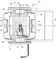
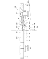
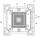
- FIG. 1 is a perspective view showing an IC socket according to an embodiment of the present invention. It is a disassembled perspective view which shows the IC socket which concerns on the same embodiment. It is a top view which shows the IC socket which concerns on the same embodiment.
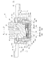
- FIG. 4 is a cross-sectional view taken along line AA of FIG. 3 in the IC socket according to the same embodiment, in which the right side is a state diagram before locking, and the left side is a state diagram at locking.
- FIG. 4 is a cross-sectional view taken along line BB of FIG. 3 in the IC socket according to the same embodiment. It is a top view which shows the state which removed the cover of the IC socket which concerns on the same embodiment.
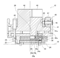
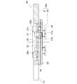
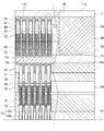
- FIG. 7 is a cross-sectional view taken along the line CC of FIG. 6 in the IC socket according to the same embodiment.
- FIG. 7 is a cross-sectional view taken along line DD of FIG. 6 in the IC socket according to the same embodiment. It is a top view which shows the state which removed the cover and upper module of the IC socket which concern on the embodiment.
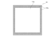
- FIG. 44E is a front view showing the appearance of the memory package according to the embodiment. 2 is a plan view showing an appearance of a memory package according to the same embodiment.
- FIG. 2 is a front view showing an appearance of a processor package according to the embodiment.
- FIG. 2 is a plan view showing an appearance of a memory package according to the same embodiment.
- FIG. It is an isotherm figure which shows the temperature distribution at the time of the heating of the IC socket which concerns on the same embodiment. It is an isotherm figure which shows the temperature distribution at the time of the heating of the IC socket which concerns on a comparative example.
- 1 to 15A show an embodiment of the present invention.
- the IC socket 10 corresponds to the “socket for electrical parts” of the present invention, and as shown in FIGS. 1 and 2, the upper module 20 as the “upper housing portion” of the present invention and the “lower side” It has a socket body 10a having a bottom module 30 as an “accommodating portion”.
- the upper module 20 accommodates the memory package 11 as the “first electrical component” of the present invention. Further, the bottom module 30 accommodates the processor package 12 as the “second electrical component” of the present invention.
- the substantially rectangular cover 40 in plan view corresponds to the “pressing member” of the present invention.
- the bottom module 30 is assembled below the cover 40 with the upper module 20 interposed therebetween.
- the memory package 11 and the processor package 12 are accommodated in a state where the memory package 11 is stacked on the upper side of the processor package 12. That is, the IC socket 10 of the present embodiment can execute the operation test of the memory package 11 and the processor package 12 in an environment close to a state where the memory package 11 and the processor package 12 are mounted so as to form a so-called package on package (PoP) structure. .
- PoP package on package
- the memory package 11 of the present embodiment is a so-called BGA (Ball Grid Array) as shown in FIGS. 13A and 13B. That is, the memory package 11 has a main body portion 11a having a substantially square shape in plan view, and a plurality of hemispherical terminals 11b projecting downward from the peripheral edge of the square frame shape on the lower surface of the main body portion 11a. Is provided.
- BGA Bit Grid Array
- the processor package 12 of this embodiment is also a so-called BGA as shown in FIGS. 14A and 14B.
- the processor package 12 has a main body 12a that is substantially square in plan view and has the same size as the main body 11a of the memory package 11.
- a plurality of hemispherical lower terminals 12b for contacting the wiring board 19 are formed on the lower surface of the main body 12a so as to protrude downward.
- a hemispherical upper terminal 12c is formed on the upper surface of the main body 12a to bring the terminal 11b of the memory package 11 into contact with the periphery of the rectangular frame shape (see FIG. 12).
- the shape of each terminal described above is not limited to a hemispherical shape, and may be another shape such as a substantially flat plate shape.
- the bottom module 30 of the IC socket 10 has a module body 30a as shown in FIG. 2 and FIG.
- the module main body 30a has a frame-shaped portion 31, and a plate-shaped contact unit 32 having a substantially square shape in plan view is fitted to the center portion thereof.
- the contact unit 32 has a lower plate member 33, an upper plate member 34, and a floating member 35.
- the floating member 35 is biased in a direction away from the lower plate member 33 and the upper plate member 34 by a spring (not shown).
- the lower plate member 33 includes an upper first lower plate member 33a and a lower second lower plate member 33b. These first and second lower plate members 33a and 33b are held by a holding member (not shown).
- the floating member 35 is brought close to the upper plate member 34 and the lower plate member 33 by being pushed down against the urging force of the above-described spring in a state where the processor package 12 is arranged in the lower arrangement portion 38 provided on the upper surface thereof. So that it can move up and down.
- a large number of contact pins 70 are arranged in the contact unit 32 in a state of being directed in the vertical direction.
- These contact pins 70 are provided between the first plunger 71 to be in contact with the lower terminal 12 b of the processor package 12, the second plunger 72 to be in contact with the wiring board 19, and the first plunger 71 and the second plunger 72.
- an urging member 73 such as a coil spring that is provided and urges the both in the direction of separating them.
- these contact pins 70 have a first plunger as shown in FIG.
- the upper end portion of 71 comes into contact with the lower terminal 12b of the processor package 12 placed on the lower arrangement portion 38 of the bottom module 30, and the lower end portion of the second plunger 72 serves as an electrode (not shown) of the wiring board 19. Contact.
- a pair of engaged pieces 30b for engaging with a pair of latches 51 of the cover 40 described later are provided on the outside of the module main body 30a.
- Each engaged piece 30b has an upper engaged portion 30c and a lower engaged portion 30d.
- the upper engaged portion 30c and the lower engaged portion 30d are both formed outward so as to face the claw portions 51a provided in the latches 51 of the cover 40.
- the vertical position difference between the upper engaged portion 30c and the lower engaged portion 30d (the height of the lower engaged portion 30d is subtracted from the height of the upper engaged portion 30c. 4
- the assembly height of the upper module 20 (that is, the position of the bottom module 30 when the upper module 20 is interposed between the cover 40 and the bottom module 30)
- the cover 40 (The difference from the position of the bottom module 30 when the upper module 20 is not interposed between the bottom module 30 and the bottom module 30).
- the claw portion 51 a provided on the latch 51 of the cover 40 is engaged with the upper engaged portion 30 c provided on the engaged piece 30 b of the bottom module 30.
- the bottom module 30 can be assembled to the cover 40 with the upper module 20 interposed.
- the upper module 20 is not interposed by engaging the claw portion 51a provided on the latch 51 of the cover 40 with the lower engaged portion 30d provided on the engaged piece 30b of the bottom module 30.
- the bottom module 30 can also be assembled to the cover 40 in the state.
- the upper module 20 has a module main body 20a as the “accommodating main body” of the present invention, as shown in FIG. 2 and FIGS.
- the module main body 20a has a frame-shaped portion 21, and a plate-shaped contact unit 22 having a substantially square shape in plan view is fitted to the center portion thereof.
- the contact unit 22 has a lower plate member 23, an upper plate member 24, and a floating member 25 as shown in FIGS. As shown in FIG. 8, the floating member 25 is biased by a spring 26 in a direction away from the lower plate member 23 and the upper plate member 24.
- the upper module 20 includes a stopper member 27 that penetrates the lower plate member 23, the upper plate member 24, and the floating member 25.
- the stopper member 27 fixes the lower plate member 23 and the upper plate member 24 by a lower screw portion 27a and a small flange portion 27b provided on the upper side thereof and wider than the screw portion 27a.
- the highest rising position of the floating member 25 is regulated by a large flange portion 27c which is provided above the small flange portion 27b and is wider than the small flange portion 27b.
- an upper arrangement portion 28 for arranging the memory package 11 is provided on the upper surface of the floating member 25, on the upper surface of the floating member 25, an upper arrangement portion 28 for arranging the memory package 11 is provided. Since the floating member 25 can be raised / lowered between the upper plate member 24 and the large flange portion 27c of the stopper member 27, the upper arrangement portion 28 can also be moved up and down between the highest raised position and the lowest lowered position. is there. In addition, guides 28 a that define the arrangement position of the memory package 11 are provided at the four corners of the upper arrangement portion 28.
- contact pins 60 are arranged below the peripheral edge of the upper arrangement portion 28 so as to face in the vertical direction.
- These contact pins 60 are a plunger 61 that contacts the terminal 11b of the memory package 11, and an urging force such as a coil spring that is inserted into the lower portion of the plunger 61 and contacts the upper terminal 12c of the processor package 12.
- Member 62 is a large number of contact pins 60 that contacts the terminal 11b of the memory package 11, and an urging force such as a coil spring that is inserted into the lower portion of the plunger 61 and contacts the upper terminal 12c of the processor package 12.
- the upper end portion of the plunger 61 is placed on the upper arrangement portion 28 of the upper module 20 as shown in FIG.
- the lower end portion of the biasing member 62 contacts the upper terminal 12c of the processor package 12 disposed on the lower placement portion 38 of the bottom module 30 with a predetermined contact pressure. To do.
- the contact unit 22 of the upper module 20 includes the lower plate member 23, the upper plate member 24, and the floating member 25 (see FIGS. 8, 8, 12 and the like). At substantially central portions of the members 23, 24, and 25, openings 23b, 24b, and 25b having substantially square shapes in plan view are provided. And these opening parts 23b, 24b, and 25b comprise the opening part 20b of the contact unit 22.
- FIG. 1 the contact unit 22 of the upper module 20 includes the lower plate member 23, the upper plate member 24, and the floating member 25 (see FIGS. 8, 8, 12 and the like).
- a substantially square heat conductive member 29 is disposed in the opening 20b in plan view.
- the heat conductive member 29 is formed so as to easily conduct heat and to have an insulating property.
- the heat conductive member 29 is formed by forming an insulating film on the surface of an aluminum member by alumite processing.
- the upper surface and the lower surface of the heat conductive member 29 are substantially flat so that the contact area between the upper surface and the memory package 11 and the contact area between the lower surface and the processor package 12 are sufficiently large. Is formed.
- the heat conductive member 29 has a flange-shaped protrusion 29a formed on the side surface so as to protrude outward over the entire circumference.
- the upper plate member 24 is provided with a notch 24a from the lower portion to the lower surface of the inner peripheral surface of the upper plate opening 24b.
- cover 40 of the IC socket 10 has a cover body 41 having a substantially rectangular parallelepiped frame shape as shown in FIGS.
- a heat sink 42 is attached to the inside of the cover body 41 so as to be movable up and down along the positioning pins 43 while being urged upward by a spring (not shown).
- the cover body 41 has a substantially U-shaped bail (operating lever) 45 that is rotatable about the shaft 46 in the directions of arrows M and N by about 180 °. Is attached. As a result, the bail 45 rotates between the standby position P1 (right side in FIG. 4) and the test position P2 (left side in FIG. 4).
- One cam 47 is attached to each end of the bail 45. These cams 47 rotate around the shaft 46 by rotating the bail 45.
- latches 51 are respectively attached to the two opposing sides on the outer peripheral surface of the cover main body 41.
- Each of these latches 51 is configured to open and close by rotating in the directions of arrows K and L around the shaft 52.
- Each latch 51 has an operation portion 51b formed at the upper end portion and a tapered claw portion 51a formed inward at the lower end portion.
- each latch 51 has two coil springs 53 provided between the operation unit 51 b at the upper end of each latch 51 and the cover main body 41.
- the operation part 51 b of the latch 51 is always urged to the outside of the cover body 41 by these coil springs 53. Accordingly, the latch 51 is always given a biasing force that rotates in the direction of the arrow L (see FIG. 4), that is, a biasing force in the closing direction.
- a pair of substantially cylindrical lock pins 49 are embedded in the cover body 41 in a state of protruding outward in the horizontal direction (that is, in a direction facing the corresponding latch 51). ing. With these lock pins 49, each latch 51 can be locked in a closed state while the heat sink 42 is pushed down.
- a heater 44 is disposed inside the heat sink 42 described above.
- the heat sink 42 is heated by the heater 44 with the heat sink 42 pressed against the memory package 11.
- the heat of the heat sink 42 heats the memory package 11 housed in the upper module 20.
- the heat generated in the heat sink 42 is conducted from the memory package 11 to the processor package 12 accommodated in the bottom module 30 through the heat conductive member 29.
- the heat sink 42 is provided with a thermocouple 44 a for managing the temperature of the heater 44.
- the temperature in the burn-in apparatus is raised to a predetermined high temperature (for example, 80 ° C.), and the temperature of the sheet sink is raised to the test temperature (for example, 120 ° C.) by the heater 44.
- the processor package 12 is accommodated on the lower arrangement portion 38 of the bottom module 30 and the memory package 11 is accommodated on the upper arrangement portion 28 of the upper module 20.
- the processor package 12 faces the lower surface of the heat conductive member 29 on the upper surface of the main body portion 12a
- the memory package 11 faces the upper surface of the heat conductive member 29 on the lower surface of the main body portion 11a.
- the claw portion 51a of the latch 51 is engaged with the engaged piece 30b of the bottom module 30 in a state where the bail 45 of the cover 40 is located at the standby position P1.
- the upper module 20 and the bottom module 30 are attached to the lower side of the cover 40.
- the bottom module 30 is assembled to the cover 40 via the upper module 20.
- the IC socket 10 is disposed on the wiring board 19, and then the bail 45 of the cover 40 is rotated in the direction of arrow N as shown on the left side of FIG. Rotate to position P2.
- the pressing portion 47b (see FIG. 5) of the cam 47 presses the upper surface of the protruding portion 42a of the heat sink 42 to lower the heat sink 42.
- the heat sink 42 lowers the memory package 11 placed on the upper arrangement portion 28 of the upper module 20 in the module body 20a.
- the contact pin 60 contacts the upper terminal 12c of the processor package 12 and the terminal 11b of the memory package 11 with a predetermined contact pressure, and the upper terminal 12c and the terminal 11b are electrically connected. (See FIG. 7).
- the processor package 12 placed on the lower arrangement portion 38 of the bottom module 30 is pushed down by the upper module 20 in the module main body 30a.
- the contact pins 70 come into contact with the electrodes (not shown) of the wiring board 19 and the lower terminals 12b of the processor package 12 with a predetermined contact pressure.
- the lower terminal 12b and the electrode of the wiring board 19 are electrically connected.
- the processor package 12 comes into contact with the lower surface of the heat conductive member 29 on the upper surface of the main body portion 12a, and the memory package 11 contacts the lower surface of the heat conductive member 29 on the lower surface of the main body portion 11a. It comes into contact with the top surface.
- the temperature in the burn-in device (not shown) is raised to a set temperature (for example, 80 ° C.).
- the heater 44 provided on the cover 40 of the IC socket 10 is turned on to heat the heat sink 42.
- the heat of the heat sink 42 is conducted to the memory package 11 and the temperature of the memory package 11 rises.
- heat is conducted from the lower surface of the main body portion 11a of the memory package 11 to the upper surface of the heat conductive member 29, and the temperature of the heat conductive member 29 rises.
- heat is conducted from the lower surface of the heat conductive member 29 to the upper surface of the main body 12a of the processor package 12, and the temperature of the processor package 12 rises.
- the surface temperature of the memory package 11 and the processor package 12 is set to a predetermined temperature (for example, 120 ° C.).
- the heat conductive member 29 is disposed between the memory package 11 and the upper module 20 so that the lower surface of the memory package 11 and the upper surface of the heat conductive member 29 are in contact with each other.
- the lower surface of the heat conductive member 29 is in contact with the upper surface of the processor package 12.
- the current is passed through two types of electrical components (the memory package 11 and the processor package 12) to perform the test.
- the burn-in test of the processor package 12 and the memory package 11 can be performed simultaneously under substantially equal temperature conditions.
- FIGS. 15A and 15B a comparative experiment between an IC socket having the thermal conductive member 29 (IC socket 10 of the present embodiment) and an IC socket not having the thermal conductive member 29 will be described. I will explain.
- the curve in the frame is an isotherm.
- the IC socket 10 according to the present embodiment was manufactured, and the memory package 11 and the processor package 12 were accommodated. At the same time, the memory package 11 and the processor package 12 were accommodated in the comparative IC socket.
- the comparative IC socket is different from the IC socket of this embodiment only in that the thermal conductive member 29 is not provided.
- the IC socket 10 has a small temperature difference between the packages 11 and 12 as shown in FIG. 15A.
- the memory package 11 is 145.75 degC
- the heat conductive member 29 is 142.04 degC
- the processor package 12 is 141.23 degC
- the temperature difference between the memory package 11 and the processor package 12 is 4.52 degC. .
- the temperature difference between the packages 11 and 12 is larger than that in the case of the IC socket 10 of the present embodiment, as shown in FIG. 15B. .
- the memory package 11 was 149.14 degC and the processor package 12 was 128.23 degC, and the temperature difference between the memory package 11 and the processor package 12 was 20.91 degC.
- the IC socket 10 according to the present embodiment having the heat conductive member 29 reduces the temperature difference between the packages 11 and 12 as compared with the state without the heat conductive member 29. I was able to.
- the heat conductive member 29 is provided in the IC socket 10 for performing a test or the like in a state where the memory package 11 and the processor package 12 are arranged one above the other. 12 were in contact with each other.
- the thermal conductivity of the thermal conductive member 29 be higher than the thermal conductivity of the module main body 20a provided in the upper module 20. According to the present embodiment, heat can be easily transferred from the upper memory package 11 to the lower processor package 12 with a simple structure, whereby a temperature difference between the upper memory package 11 and the lower processor package 12 can be achieved. Can be reduced. As a result, the test can be performed with the memory package 11 and the processor package 12 in a state close to the set temperature state.
- the heat conductive member 29 is disposed in the opening 20b provided in the substantially central portion of the upper module 20, both the memory package 11 and the processor package 12 are used.
- the contact can be made in a wide area. Also in this respect, the temperature difference between the memory package 11 and the processor package 12 can be reduced.
- the IC socket 10 of the present embodiment since the surface of the heat conductive member 29 is insulative, the plurality of terminals 11b of the package 11 and the plurality of upper terminals 12c of the package 12 are electrically connected. A short circuit can be prevented.
- the IC socket 10 of the present embodiment is provided with a heat sink 42 above the upper module 20, and by providing a heater 44 on the heat sink 42, the temperature that can be set by the burn-in device in which the IC socket 10 is disposed
- the memory package 11 and the processor package 12 can be further heated.
- the heat conductive member 29 is disposed between the memory package 11 and the processor package 12 as described above, the memory package 11 and the processor are connected to each other even though the upper surface of the memory package 11 is heated by the heat sink 42.
- the temperature difference with the package 12 can be very small.
- the IC socket 10 of this embodiment is suitable for use in testing an IC package mounted on a mounting circuit having a so-called package-on-package structure.
- the package-on-package structure is a mounting method in which two IC packages are stacked so as to be in direct contact with each other on a circuit board.
- the heat conductive member 29 is disposed between two IC packages (that is, the memory package 11 and the processor package 12), the temperature condition is very close to the mounting circuit of the package-on-package structure. Thus, these two IC packages can be tested.
- the memory package 11 is heated from the upper surface using the heat sink 42.
- the present invention can also be applied to an IC socket that is not heated by the heat sink 42 or the like, and in that case, the effect of reducing the temperature difference between the two IC packages stacked one above the other can be obtained. it can.
- the present invention is not limited to this, and can be applied to sockets that accommodate other types of electrical parts.
- the IC socket according to the present embodiment is suitable for testing an IC package applied to a packaged circuit having a package-on-package structure, but of course, it can also be used for testing a mounted circuit other than the package-on-package structure. It is.
- IC socket (socket for electrical parts) 10a socket body 11 memory package (first electrical component) 12 Processor package (second electrical component) 19 Wiring board 20 Upper module (upper housing) 20a Module body (housing body) 20b Opening 29 Thermally conductive member 30 Bottom module (lower housing part) 40 Cover (pressing member) 44 Heater
Landscapes
- Engineering & Computer Science (AREA)
- Physics & Mathematics (AREA)
- General Physics & Mathematics (AREA)
- Computer Hardware Design (AREA)
- Microelectronics & Electronic Packaging (AREA)
- General Engineering & Computer Science (AREA)
- Environmental & Geological Engineering (AREA)
- Testing Of Individual Semiconductor Devices (AREA)
- Connecting Device With Holders (AREA)
Abstract
【課題】2個の電気部品が上下に配置された状態で試験等を行う電気部品用ソケットにおいて、これら2個の電気部品の温度差を低減する。 【解決手段】 本発明の電気部品用ソケットは、第1の電気部品を収容する上側収容部と、第2の電気部品を収容する下側収容部とを有する。上側収容部は、開口部を有する収容本体と、該開口部に配設されて収容本体よりも熱伝導率の高い熱伝導性部材とを有する。この熱伝導性部材は、上側収容部に収容された第1の電気部品と下側収容部に収容された第2の電気部品の双方に接触するように配置される。
Description
本発明は、配線基板上に配設されて、半導体装置(以下「ICパッケージ」という)等の電気部品の試験等を行うためにこの電気部品を収容する、電気部品用ソケットに関するものである。
従来、ICパッケージを着脱自在に収容して、そのICパッケージの動作試験を行うためのICソケットがある。
また、そのような動作試験用のICソケットとして、複数個のICパッケージを同時に収容して動作試験を行うものが知られている(特許文献1参照)。
更に、これら複数個のICパッケージをヒータでそれぞれ加熱して、高温下での動作試験を行うICソケットが、知られている。
しかしながら、従来のICソケットでは、複数個のICパッケージに対して同時に高温下で動作試験を行う際に、これら複数個のICパッケージに温度差が生じる虞があり、このため、これら複数のICパッケージに対して、意図した温度で信頼性の高い動作試験を行うことが難しかった。
そこで、本発明は、複数の電気部品を同時に収容して動作試験を行う際に、それら電気部品間の温度差を十分に小さい状態にできる電気部品用ソケットを提供することを課題としている。
かかる課題を達成するために、本発明に係る電気部品用ソケットは、第1の電気部品と第2の電気部品が収容されて配線基板上に配設される電気部品用ソケットであって、前記配線基板上に配設され、前記第1の電気部品と前記第2の電気部品を収容するソケット本体を有し、該ソケット本体は、前記第1の電気部品を収容する上側収容部と、前記第2の電気部品を収容する下側収容部とを有しており、前記上側収容部は、開口部を有する収容本体と、該開口部に配設されて前記収容本体よりも熱伝導率の高い熱伝導性部材とを有しており、該熱伝導性部材が、前記上側収容部に収容された前記第1の電気部品と前記下側収容部に収容された前記第2の電気部品の双方に接触するように構成されていることを特徴とする。
本発明の電気部品用ソケットにおいて、前記開口部は、前記上側収容部の略中央部に設けられることが望ましい。
本発明の電気部品用ソケットにおいて、前記熱伝導性部材は、絶縁性を有していることが望ましい。
本発明の電気部品用ソケットにおいて、前記熱伝導性部材は、前記第1の電気部品の本体下面と接すると共に、前記第2の電気部品の本体上面と接するように配置されることが望ましい。
本発明の電気部品用ソケットにおいては、前記第1の電気部品の本体上面を加熱する加熱機構を更に有することが望ましい。
本発明の電気部品用ソケットにおいて、前記加熱機構は、前記第1の電気部品の前記本体上面を押圧するヒートシンクと、該ヒートシンクを加熱するヒータとを有することが望ましい。
本発明の電気部品用ソケットにおいて、前記第1の電気部品及び前記第2の電気部品は、上下に積み重ねられた状態で回路基板に実装される2個のICパッケージであることが望ましい。
本発明によれば、上側収容部に収容された第1の電気部品と下側収容部に収容された第2の電気部品の双方に接触するように、上側収容部にその収容本体よりも熱伝導率の高い熱伝導性部材を配設したため、簡単な構造で、上下の電気部品同士で熱を伝わり易くすることができ、これにより、上下の電気部品の温度差を小さくできる。その結果、上下の電気部品を、予め設定した温度に近い状態にして試験を行うことができる。
本発明において、上側収容部の略中央部に開口部を設けてその開口部に熱伝導性部材を配置することにより、この熱伝導性部材を、第1の電気部品及び第2の電気部品の双方に、十分に広い面積で接触させることができる。そのため、上下の電気部品の温度差を、十分に小さくすることができる。
本発明において、絶縁性の熱伝導性部材を使用することにより、第1及び第2の電気部品の、端子間での短絡を防止できる。
本発明において、熱伝導性部材を、第1の電気部品の本体下面と接すると共に第2の電気部品の本体上面と接するように配置することにより、この熱伝導性部材を、第1の電気部品及び第2の電気部品の双方に、十分に広い面積で接触させることができる。そのため、上下の電気部品の温度差を、十分に小さくすることができる。
本発明によれば、熱伝導部材を設けたので、第1の電気部品の本体上面を加熱する加熱機構を設けた場合に、この加熱機構で発生した熱を第1及び第2の電気部品へ略均等に伝導させることができる。
本発明において、ヒータを有するヒートシンクで第1の電気部品の本体上面を押圧しながら加熱することにより、第1の電気部品の固定と加熱とを有効に行うことができる。
本発明において、ヒータを有するヒートシンクで第1の電気部品の本体上面を押圧しながら加熱することにより、第1の電気部品の固定と加熱とを有効に行うことができる。
本発明によれば、上下に積み重ねられた状態で回路基板に実装される2個のICパッケージの試験を、実装状態に近い条件下で行うことができる。
以下、本発明の実施形態について説明する。
図1~図15Aには、本発明の実施形態を示す。
まず構成を説明する。
本実施形態に係るICソケット10は、本発明の「電気部品用ソケット」に相当し、図1及び図2に示すように、本発明の「上側収容部」としてのアッパーモジュール20と「下側収容部」としてのボトムモジュール30を有するソケット本体10aを有している。
アッパーモジュール20には、本発明の「第1の電気部品」としてのメモリパッケージ11が収容される。また、ボトムモジュール30には、本発明の「第2の電気部品」としてのプロセッサパッケージ12が収容される。
平面視略四角形のカバー40は、本発明の「押圧部材」に相当する。このカバー40の下側には、アッパーモジュール20を挟んで、ボトムモジュール30が組み付けられる。
そして、図4に示すように、配線基板19上にボトムモジュール30を配設することにより、2種類の電気部品(すなわち、メモリパッケージ11及びプロセッサパッケージ12)を、同時に試験することができる。
このように、本実施形態のICソケット10では、メモリパッケージ11とプロセッサパッケージ12とが、プロセッサパッケージ12の上側にメモリパッケージ11が積層された状態で収容される。すなわち、本実施形態のICソケット10は、メモリパッケージ11及びプロセッサパッケージ12の動作試験を、所謂パッケージオンパッケージ(PoP)構造を成すように実装された状態に近い環境下で、実行することができる。
本実施形態のメモリパッケージ11は、図13A及び図13Bに示すように、所謂BGA(Ball Grid Array)である。すなわち、このメモリパッケージ11は、平面視略正方形の本体部11aを有し、また、この本体部11aの下面には、四角枠形状の周縁部から下向きに突出する、複数の半球状の端子11bが設けられている。
また、本実施形態のプロセッサパッケージ12も、図14A及び図14Bに示すように、所謂BGAである。このプロセッサパッケージ12は、平面視で略正方形の、メモリパッケージ11の本体部11aと同様の大きさの本体部12aを有する。そして、この本体部12aの下面には、配線基板19に接触させるための複数の半球状の下側端子12bが、下向きに突出して形成されている。また、本体部12aの上面には、四角枠形状の周縁部に、メモリパッケージ11の端子11bを接触させて導通させるための、半球状の上側端子12cが形成されている(図12参照)。なお、上記した各端子の形状は、半球状に限るものではなく、略平板状等の他の形状であっても良い。
一方、ICソケット10のボトムモジュール30は、図2や図10に示すように、モジュール本体30aを有している。このモジュール本体30aは、枠状部31を有しており、その中央部には、平面視が略正方形で板状のコンタクトユニット32が嵌合されている。このコンタクトユニット32は、図11、12に示すように、下板部材33と上板部材34とフローティング部材35を有している。フローティング部材35は、スプリング(図示省略)によって、下板部材33及び上板部材34から離れる方向へ付勢されている。下板部材33は、上側の第1下板部材33aと下側の第2下板部材33bとで構成されている。これら第1、第2下板部材33a,33bが図示しない保持部材によって保持されている。フローティング部材35は、その上面に設けられた下側配置部38にプロセッサパッケージ12を配置した状態で、上述のスプリングの付勢力に逆らって押し下げることで、上板部材34と下板部材33に近づけることができるように、上下動自在に支持されている。
また、このコンタクトユニット32には、図10~12に示すように、多数のコンタクトピン70が、上下方向を向いた状態で配設されている。
これらのコンタクトピン70は、プロセッサパッケージ12の下側端子12bに当接させる第1プランジャ71と、配線基板19に当接させる第2プランジャ72と、第1プランジャ71と第2プランジャ72の間に設けられて双方を離間する方向に付勢する、コイルスプリング等の付勢部材73とを有している。
これらのコンタクトピン70は、ボトムモジュール30及びアッパーモジュール20がカバー40に組み付けられて配線基板19上に設置された状態(図4参照)では、図11(b)に示すように、第1プランジャ71の上端部がボトムモジュール30の下側配置部38に載置されたプロセッサパッケージ12の下側端子12bに接触するとともに、第2プランジャ72の下端部が配線基板19の電極(図示省略)に接触する。
さらに、モジュール本体30aの外側には、図4に示すように、後述するカバー40の一対のラッチ51と係合させるための、一対の被係合片30bが設けられている。各被係合片30bは、それぞれ、上側被係合部30cおよび下側被係合部30dを有している。これらの上側被係合部30c、下側被係合部30dは、いずれも、カバー40の各ラッチ51に設けられた爪部51aに対向するように、外向きに形成されている。
ここで、上側被係合部30cと下側被係合部30dとの、上下方向の位置の差(上側被係合部30cの高さから下側被係合部30dの高さを減じたもの)は、図4に示すように、アッパーモジュール20の組付高さ(すなわち、カバー40とボトムモジュール30との間にアッパーモジュール20を介在させたときのボトムモジュール30の位置と、カバー40ボトムモジュール30との間にアッパーモジュール20を介在させなかったときのボトムモジュール30の位置との差)にほぼ等しくなっている。
そのため、ICソケット10では、図4に示すように、カバー40のラッチ51に設けた爪部51aをボトムモジュール30の被係合片30bに設けた上側被係合部30cに係合させることにより、アッパーモジュール20を介在させた状態でボトムモジュール30をカバー40に組み付けることができる。その一方で、カバー40のラッチ51に設けた爪部51aをボトムモジュール30の被係合片30bに設けた下側被係合部30dに係合させることにより、アッパーモジュール20を介在させていない状態でボトムモジュール30をカバー40に組み付けることもできる。
アッパーモジュール20は、図2及び図4~6に示すように、本発明の「収容本体」としてのモジュール本体20aを有している。このモジュール本体20aは、枠状部21を有しており、その中央部には、平面視が略正方形で板状のコンタクトユニット22が嵌合されている。このコンタクトユニット22は、図8,9,12に示すように、下板部材23と上板部材24とフローティング部材25を有している。図8に示したように、フローティング部材25は、スプリング26によって、下板部材23と上板部材24から離れる方向へ付勢されている。
また、アッパーモジュール20は、下板部材23と上板部材24とフローティング部材25とを貫通する、ストッパ部材27を有している。このストッパ部材27は、下方のネジ部27aと、その上側に設けられた、そのネジ部27aより幅広の小フランジ部27bとによって、下板部材23と上板部材24とを固定する。さらに、小フランジ部27bの上側に設けられた、その小フランジ部27bより幅広の大フランジ部27cによって、フローティング部材25の最上昇位置を規制している。
そして、このフローティング部材25の上面には、メモリパッケージ11を配置するための、上側配置部28が設けられている。このフローティング部材25は、上板部材24とストッパ部材27の大フランジ部27cの間で上昇/下降できるので、この上側配置部28も、最上昇位置と最下降位置との間で上下動可能である。また、この上側配置部28の四隅には、メモリパッケージ11の配置位置を規定するガイド28aが設けられている。
また、この上側配置部28の周縁部の下方には、図6,7,12に示すように、多数のコンタクトピン60が上下方向を向いた状態で配設されている。これらのコンタクトピン60は、メモリパッケージ11の端子11bに当接されるプランジャ61と、当該プランジャ61の下部に挿入されてプロセッサパッケージ12の上側端子12cに当接される、コイルスプリング等の付勢部材62とを有している。
そして、ボトムモジュール30及びアッパーモジュール20がカバー40に組み付けられた状態(図1参照)では、図7(b)に示すように、プランジャ61の上端部がアッパーモジュール20の上側配置部28上に配置されたメモリパッケージ11の端子11bに接触するとともに、付勢部材62の下端部がボトムモジュール30の下側配置部38上に配置されたプロセッサパッケージ12の上側端子12cに所定の接圧で接触する。
上述のように、アッパーモジュール20のコンタクトユニット22は、下板部材23、上板部材24及びフローティング部材25を備えている(図8、8、12等参照)。部材23,24,25の略中央部には、平面視で略正方形の開口部23b,24b,25bが設けられている。そして、これら開口部23b,24b,25bによって、コンタクトユニット22の開口部20bが構成されている。
この開口部20bには、図6に示すように、平面視で略正方形の熱伝導性部材29が配設されている。この熱伝導性部材29は、熱を伝導しやすく、かつ、絶縁性を有するように形成される。本実施形態では、アルミニウム部材の表面にアルマイト加工処理で絶縁膜を形成したものを、この熱伝導性部材29として使用する。
また、この熱伝導性部材29は、その上面とメモリパッケージ11との接触面積や、その下面とプロセッサパッケージ12との接触面積が、十分に大きくなるように、その上面及び下面が略平面状に形成されている。
図5に示したように、この熱伝導性部材29は、その側面に、その全周に渡って外側に突出するように形成された、フランジ状の突出部29aを有している。一方、上板部材24には、上板開口部24bの内周面の下部から下面にかけて、切欠部24aが設けられている。この切欠部24aに熱伝導性部材29の突出部29aを挿入した状態で、上板部材24の下面に下板部材23の上面を当接させることにより、この突出部29aが下板部材23と上板部材24とで挟み込まれた状態になる。そして、これら下板部材23と上板部材24とをストッパ部材27で固定することにより、アッパーモジュール20の開口部20bに熱伝導性部材29を収容して保持することができる。
また、ICソケット10のカバー40は、図2~図5に示すように、略直方体枠形状のカバー本体41を有している。このカバー本体41の内側には、ヒートシンク42が、スプリング(図示省略)によって上方へ付勢された状態で、位置決めピン43に沿って上下動自在に取り付けられている。
さらに、図1、図2及び図4に示すように、カバー本体41には、略コ字形のベール(操作レバー)45が、シャフト46を中心として矢印M、N方向に約180°回動自在に、取り付けられている。これにより、このベール45が、待機位置P1(図4の右側)と試験位置P2(図4の左側)との間で、回転移動する。
このベール45の両端部には、カム47が1個ずつ取り付けられている。これらのカム47は、ベール45を回転させることにより、シャフト46を中心として回転する。
ベール45が待機位置P1に位置するとき(図4の左側)、図5に示すように、カム47の押下部47aは最上昇位置にあり、ヒートシンク42の突出部42aを押圧しない。このため、図示しないスプリングの付勢力によって、ヒートシンク42が押し上げられた状態にある。一方、ベール45を試験位置P2まで回転移動させたとき(図4の右側)、カム47の押下部47aが加工してヒートシンク42の突出部42aの上面に接触し、スプリングの付勢力に抗してヒートシンク42を押し下げる。
また、カバー本体41の外周面には、図4に示すように、対向する2辺にそれぞれ、ラッチ51が取り付けられている。これらのラッチ51は、それぞれ、シャフト52を中心として、矢印K、L方向に回転することによって開閉するように構成されている。各ラッチ51には、それぞれ、上端部に操作部51bが形成されているとともに、下端部にテーパ状の爪部51aが内向きに形成されている。
図3に示したように、各ラッチ51の上端部の操作部51bとカバー本体41との間には、それぞれ、2個ずつのコイルスプリング53が設けられている。ラッチ51の操作部51bは、これらのコイルスプリング53によって、常に、カバー本体41の外側に付勢されている。これにより、ラッチ51には、常に、矢印L方向(図4参照)に回転する付勢力、すなわち閉じる方向の付勢力が与えられる。
さらに、カバー本体41には、図4に示すように、一対の略円柱状のロックピン49が、水平方向外向き(すなわち、対応するラッチ51に対向する方向)に突出した状態で、埋設されている。これらのロックピン49により、ヒートシンク42が押し下げられた状態で、各ラッチ51を閉じた状態にロックすることができる。
上述のヒートシンク42の内部には、図3に示すように、ヒータ44が配設されている。試験時には、ヒートシンク42をメモリパッケージ11に押し当てた状態で、このヒータ44で、このヒートシンク42を加熱する。その結果、このヒートシンク42の熱で、アッパーモジュール20に収容されたメモリパッケージ11が加熱される。さらに、ヒートシンク42で発生した熱は、このメモリパッケージ11から熱伝導性部材29を介して、ボトムモジュール30に収容されたプロセッサパッケージ12へ伝導する。
ヒートシンク42には、ヒータ44の温度を管理するための、熱電対44aが設けられている。
なお、通常のバーンイン装置では、装置内部の温度を所定の試験温度(例えば120℃)まで上昇させることは容易ではない。このため、本実施形態では、バーンイン装置内の温度を所定の高温(例えば80℃)まで上昇させると共に、ヒータ44でシートシンクの温度を試験温度(例えば120℃)まで上昇させる。
次に、かかるICソケット10を用いて、2種類の電気部品(本実施形態ではメモリパッケージ11及びプロセッサパッケージ12)の試験(本実施形態ではバーンイン試験)を行う手順を、説明する。
まず、図2に示すように、ボトムモジュール30の下側配置部38上にプロセッサパッケージ12を収容するとともに、アッパーモジュール20の上側配置部28上にメモリパッケージ11を収容する。これにより、プロセッサパッケージ12が本体部12aの上面で熱伝導性部材29の下面と対向すると共に、メモリパッケージ11が本体部11aの下面でこの熱伝導性部材29の上面と対向する状態になる。
次に、図4の右側に示すように、カバー40のベール45が待機位置P1に位置している状態で、ラッチ51の爪部51aをボトムモジュール30の被係合片30bに係合させることにより、カバー40の下側にアッパーモジュール20及びボトムモジュール30を取り付ける。これにより、ボトムモジュール30はアッパーモジュール20を介してカバー40に組み付けられた状態となる。
次に、図4に示すように、このICソケット10を配線基板19上に配設し、その後、図4の左側に示すように、カバー40のベール45を矢印N方向に回動して試験位置P2まで回転させる。この回転に伴って、カム47の押下部47b(図5参照)がヒートシンク42の突出部42aの上面を押圧して、このヒートシンク42を下降させる。
その結果、ヒートシンク42が、アッパーモジュール20の上側配置部28に載置されたメモリパッケージ11をモジュール本体20a内で下降させる。これにより、コンタクトピン60が、プロセッサパッケージ12の上側端子12cと、メモリパッケージ11の端子11bとに、所定の接圧で接触して、これら上側端子12cと端子11bとが電気的に接続される(図7参照)。
それとともに、ボトムモジュール30の下側配置部38に載置されたプロセッサパッケージ12が、モジュール本体30a内で、アッパーモジュール20に押し下げられる。これにより、コンタクトピン70が、配線基板19の電極(図示省略)と、プロセッサパッケージ12の下側端子12bとに、所定の接圧でそれぞれ接触する。これにより、下側端子12bと配線基板19の電極とが、電気的に接続される。
また、ヒートシンク42の下降に伴い、図4の左側に示すように、一対のロックピン49が下降して一対のラッチ51の段差部51cに嵌合される。その結果、これらのラッチ51が閉じた状態にロックされる。
加えて、ヒートシンク42の下降に伴って、プロセッサパッケージ12が本体部12aの上面で熱伝導性部材29の下面に接触すると共に、メモリパッケージ11が本体部11aの下面でこの熱伝導性部材29の上面に接触した状態になる。
その後、バーンイン装置(図示省略)内の温度を、設定温度(例えば80℃)まで上昇させる。更に、ICソケット10のカバー40に設けられたヒータ44をオンにして、ヒートシンク42を加熱する。その結果、このヒートシンク42の熱がメモリパッケージ11に伝導して、このメモリパッケージ11の温度が上昇する。そして、メモリパッケージ11の本体部11aの下面から熱伝導性部材29の上面へ熱が伝導して、この熱伝導性部材29の温度が上昇する。更に、この熱伝導性部材29の下面からプロセッサパッケージ12の本体部12aの上面へ熱が伝導して、このプロセッサパッケージ12の温度が上昇する。このようにして、本実施形態では、メモリパッケージ11及びプロセッサパッケージ12の表面温度を、所定温度(例えば120℃)に設定する。
上述のように、本実施形態では、メモリパッケージ11とアッパーモジュール20との間に熱伝導性部材29を配置して、メモリパッケージ11の下面と熱伝導性部材29の上面とが接すると共に、この熱伝導性部材29の下面とプロセッサパッケージ12の上面とが接するようにした。
その結果、メモリパッケージ11とプロセッサパッケージ12との間で、熱を伝わり易くでき、従って、これらパッケージ11,12の温度差を小さくできる。
この状態で、2種類の電気部品(メモリパッケージ11とプロセッサパッケージ12)に電流を流して試験を行う。
以上説明したように、本実施形態によれば、プロセッサパッケージ12及びメモリパッケージ11のバーンイン試験を、略等しい温度条件で、同時に行うことができる。
次に、熱伝導性部材29を備えたICソケット(本実施形態のICソケット10)と、熱伝導性部材29を有していないICソケットとの比較実験について、図15A及び図15Bを参照して説明する。図15において、枠内の曲線は、等温線である。
この実験では、まず、本実施形態に係るICソケット10を作製して、メモリパッケージ11及びプロセッサパッケージ12を収容した。また、同時に、比較用のICソケットに、メモリパッケージ11及びプロセッサパッケージ12を収容した。比較用のICソケットは、熱伝導性部材29を備えていない点のみが、本実施形態のICソケットと異なる。
続いて、これら2種類のICソケットを、ヒータ150degC(固定)、風無し、環境温度25degC(室温)にて加熱した。そして、温度が上昇して安定した状態で、メモリパッケージ11及びプロセッサパッケージ12の温度を測定した。また、本実施形態に係るICソケット10については、熱伝導性部材29の温度も測定した。
その結果、本実施形態に係るICソケット10は、図15Aに示すようにパッケージ11,12の温度差が小さい状態となった。具体的には、メモリパッケージ11が145.75degC、熱伝導性部材29が142.04degC、プロセッサパッケージ12が141.23degCとなり、メモリパッケージ11とプロセッサパッケージ12との温度差は4.52degCとなった。
これに対し、熱伝導性部材29が設けられていないICソケットでは、図15Bに示すように、パッケージ11,12の温度差が、本実施形態のICソケット10の場合よりも大きい状態となった。具体的には、メモリパッケージ11が149.14degC、プロセッサパッケージ12が128.23degCとなり、メモリパッケージ11とプロセッサパッケージ12との温度差は20.91degCとなった。
このように、熱伝導性部材29を有している本実施形態に係るICソケット10は、熱伝導性部材29を有していない状態と比べて、パッケージ11,12の温度差を小さくすることができた。
以上説明したように、本実施形態では、メモリパッケージ11とプロセッサパッケージ12が上下に配置された状態で試験等を行うICソケット10に、熱伝導性部材29を設けて、メモリパッケージ11及びプロセッサパッケージ12の双方に接触するようにした。
ここで、熱伝導性部材29の熱伝導率は、アッパーモジュール20に設けられたモジュール本体20aの熱伝導率よりも高くすることが望ましい。本実施形態によれば、簡単な構造で、上側のメモリパッケージ11から下側のプロセッサパッケージ12へ熱を伝わり易くでき、これにより、上側のメモリパッケージ11と下側のプロセッサパッケージ12との温度差を小さくできる。その結果、メモリパッケージ11とプロセッサパッケージ12を、設定した温度状態に近い状態にして試験を行うことができる。
また、本実施形態のICソケット10では、熱伝導性部材29が、アッパーモジュール20の略中央部に設けられた開口部20bに配設されているため、メモリパッケージ11とプロセッサパッケージ12の双方により広い面積で当接させることができる。この点でも、メモリパッケージ11とプロセッサパッケージ12の温度差を小さくすることができる。
また、本実施形態のICソケット10によれば、熱伝導性部材29の表面が絶縁性を有しているため、これらパッケージ11の複数の端子11bやパッケージ12の複数の上側端子12cが電気的に短絡することを防止できる。
また、本実施形態のICソケット10は、アッパーモジュール20の上方にヒートシンク42を設けると共に、このヒートシンク42にヒータ44を設けることにより、ICソケット10を配置するバーンイン装置で設定可能な温度よりも、メモリパッケージ11及びプロセッサパッケージ12をさらに高温にすることができる。加えて、上述のように、メモリパッケージ11とプロセッサパッケージ12の間に熱伝導性部材29を配置したので、メモリパッケージ11の上面をヒートシンク42で加熱するにも拘わらず、このメモリパッケージ11とプロセッサパッケージ12との温度差を非常に小さくできる。
本実施形態のICソケット10は、いわゆるパッケージオンパッケージ構造の実装回路に搭載するICパッケージの試験に使用して好適である。周知のように、パッケージオンパッケージ構造とは、回路基板上に、二個のICパッケージを直接接するように積み重ねる実装方法である。本実施形態のICソケット10は、二個のICパッケージ(すなわちメモリパッケージ11及びプロセッサパッケージ12)の間に熱伝導性部材29を配置したので、パッケージオンパッケージ構造の実装回路に非常に近い温度条件で、これら二個のICパッケージの試験を行うことができる。
上述のように、本実施形態では、ヒートシンク42を用いてメモリパッケージ11を上面から加熱することとした。しかし、本発明は、ヒートシンク42等による加熱を行わないICソケットにも適用することができ、その場合にも、上下に積み重ねた2個のICパッケージの温度差を減らせるという効果を得ることができる。
なお、本実施形態では、「電気部品用ソケット」としてICソケット10を採用した場合を説明したが、これに限らず、他の種類の電気部品を収容するソケットにも適用できることは勿論である。
上述のように、本実施形態のICソケットは、パッケージオンパッケージ構造の実装回路に適用するICパッケージの試験に適しているが、パッケージオンパッケージ構造以外の実装回路の試験にも使用できることは、勿論である。
10 ICソケット(電気部品用ソケット)
10aソケット本体
11 メモリパッケージ(第1の電気部品)
12 プロセッサパッケージ(第2の電気部品)
19 配線基板
20 アッパーモジュール(上側収容部)
20a モジュール本体(収容本体)
20b 開口部
29 熱伝導性部材
30 ボトムモジュール(下側収容部)
40 カバー(押圧部材)
44 ヒータ
10aソケット本体
11 メモリパッケージ(第1の電気部品)
12 プロセッサパッケージ(第2の電気部品)
19 配線基板
20 アッパーモジュール(上側収容部)
20a モジュール本体(収容本体)
20b 開口部
29 熱伝導性部材
30 ボトムモジュール(下側収容部)
40 カバー(押圧部材)
44 ヒータ
Claims (7)
- 第1の電気部品と第2の電気部品が収容されて配線基板上に配設される電気部品用ソケットであって、
前記配線基板上に配設され、前記第1の電気部品と前記第2の電気部品を収容するソケット本体を有し、
該ソケット本体は、前記第1の電気部品を収容する上側収容部と、前記第2の電気部品を収容する下側収容部とを有しており、
前記上側収容部は、開口部を有する収容本体と、該開口部に配設されて前記収容本体よりも熱伝導率の高い熱伝導性部材とを有しており、
該熱伝導性部材が、前記上側収容部に収容された前記第1の電気部品と前記下側収容部に収容された前記第2の電気部品の双方に接触するように構成されていることを特徴とする電気部品用ソケット。 - 前記開口部は、前記上側収容部の略中央部に設けられていることを特徴とする請求項1に記載の電気部品用ソケット。
- 前記熱伝導性部材は、絶縁性を有していることを特徴とする請求項1に記載の電気部品用ソケット。
- 前記熱伝導性部材は、前記第1の電気部品の本体下面と接すると共に、前記第2の電気部品の本体上面と接するように配置されたことを特徴とする請求項1に記載の電気部品用ソケット。
- 前記第1の電気部品の本体上面を加熱する加熱機構を更に有することを特徴とする請求項4に記載の電気部品用ソケット。
- 前記加熱機構は、前記第1の電気部品の前記本体上面を押圧するヒートシンクと、該ヒートシンクを加熱するヒータとを有することを特徴とする請求項5に記載の電気部品用ソケット。
- 前記第1の電気部品及び前記第2の電気部品は、上下に積み重ねられた状態で回路基板に実装される2個のICパッケージであることを特徴とする請求項1に記載の電気部品用ソケット。
Priority Applications (1)
| Application Number | Priority Date | Filing Date | Title |
|---|---|---|---|
| KR1020197004049A KR102362735B1 (ko) | 2016-08-09 | 2017-07-31 | 전기 부품용 소켓 |
Applications Claiming Priority (2)
| Application Number | Priority Date | Filing Date | Title |
|---|---|---|---|
| JP2016156950A JP6744173B2 (ja) | 2016-08-09 | 2016-08-09 | 電気部品用ソケット |
| JP2016-156950 | 2016-08-09 |
Publications (1)
| Publication Number | Publication Date |
|---|---|
| WO2018030197A1 true WO2018030197A1 (ja) | 2018-02-15 |
Family
ID=61163272
Family Applications (1)
| Application Number | Title | Priority Date | Filing Date |
|---|---|---|---|
| PCT/JP2017/027711 Ceased WO2018030197A1 (ja) | 2016-08-09 | 2017-07-31 | 電気部品用ソケット |
Country Status (4)
| Country | Link |
|---|---|
| JP (1) | JP6744173B2 (ja) |
| KR (1) | KR102362735B1 (ja) |
| TW (1) | TWI724221B (ja) |
| WO (1) | WO2018030197A1 (ja) |
Families Citing this family (2)
| Publication number | Priority date | Publication date | Assignee | Title |
|---|---|---|---|---|
| TWI819598B (zh) * | 2020-02-07 | 2023-10-21 | 美商莫仕有限公司 | 計算系統 |
| JP7730671B2 (ja) * | 2021-06-10 | 2025-08-28 | Ntt株式会社 | Icソケット及びicモジュールの検査方法 |
Citations (4)
| Publication number | Priority date | Publication date | Assignee | Title |
|---|---|---|---|---|
| JPH0587873A (ja) * | 1991-03-08 | 1993-04-06 | Hewlett Packard Co <Hp> | 集積回路チツプのバーンイン選別方法および装置 |
| JP2000304804A (ja) * | 1999-04-26 | 2000-11-02 | Denken Eng Kk | バーンイン装置及びバーンイン方法 |
| JP2015158493A (ja) * | 2014-02-21 | 2015-09-03 | センサータ テクノロジーズ マサチューセッツ インコーポレーテッド | パッケージオンパッケージ熱強制デバイス |
| WO2017138522A1 (ja) * | 2016-02-08 | 2017-08-17 | 株式会社エンプラス | 電気部品用ソケット |
Family Cites Families (16)
| Publication number | Priority date | Publication date | Assignee | Title |
|---|---|---|---|---|
| JPH08213128A (ja) * | 1995-02-08 | 1996-08-20 | Texas Instr Japan Ltd | ソケット |
| US6323665B1 (en) * | 1997-10-07 | 2001-11-27 | Reliability Incorporated | Apparatus capable of high power dissipation during burn-in of a device under test |
| US6744269B1 (en) * | 1997-10-07 | 2004-06-01 | Reliability Incorporated | Burn-in board with adaptable heat sink device |
| KR101153734B1 (ko) * | 2007-02-23 | 2012-06-08 | 가부시키가이샤 어드밴티스트 | 전자부품 압압 장치 및 전자부품 시험장치 |
| JP4868413B2 (ja) * | 2007-12-04 | 2012-02-01 | センサータ テクノロジーズ インコーポレーテッド | ソケット |
| KR20080030046A (ko) * | 2008-01-24 | 2008-04-03 | 가부시키가이샤 어드밴티스트 | 푸셔, 푸셔 유닛 및 반도체 시험 장치 |
| WO2009096207A1 (ja) * | 2008-01-30 | 2009-08-06 | Seiko Instruments Inc. | 駆動モジュールおよびそれを備える電子機器 |
| KR101168036B1 (ko) * | 2010-06-17 | 2012-07-27 | 주식회사 아이에스시 | 반도체 패키지용 검사소켓 |
| JP2012237669A (ja) * | 2011-05-12 | 2012-12-06 | Advantest Corp | 電子部品試験装置、ソケットボード組立体、及びインタフェース装置 |
| JP2013008499A (ja) | 2011-06-23 | 2013-01-10 | Tdk Corp | ソケット |
| KR101246105B1 (ko) * | 2011-07-07 | 2013-03-20 | 주식회사 오킨스전자 | 반도체 패키지 테스트용 소켓 |
| KR101464990B1 (ko) | 2013-12-24 | 2014-11-26 | 주식회사 아이에스시 | 반도체 디바이스 얼라인 소켓유닛 및 이를 포함하는 반도체 디바이스 검사장치 |
| KR101528172B1 (ko) | 2014-02-11 | 2015-06-12 | 리노공업주식회사 | 검사장치 |
| JP6251104B2 (ja) * | 2014-03-31 | 2017-12-20 | 株式会社エンプラス | 昇降機構及び電気部品用ソケット |
| JP6351334B2 (ja) * | 2014-03-31 | 2018-07-04 | 株式会社エンプラス | ラッチ機構及び電気部品用ソケット |
| KR20160051146A (ko) * | 2014-10-31 | 2016-05-11 | (주)마이크로컨텍솔루션 | 테스트 소켓 및 테스트 소켓 구조체 |
-
2016
- 2016-08-09 JP JP2016156950A patent/JP6744173B2/ja not_active Expired - Fee Related
-
2017
- 2017-07-31 WO PCT/JP2017/027711 patent/WO2018030197A1/ja not_active Ceased
- 2017-07-31 KR KR1020197004049A patent/KR102362735B1/ko not_active Expired - Fee Related
- 2017-08-07 TW TW106126541A patent/TWI724221B/zh not_active IP Right Cessation
Patent Citations (4)
| Publication number | Priority date | Publication date | Assignee | Title |
|---|---|---|---|---|
| JPH0587873A (ja) * | 1991-03-08 | 1993-04-06 | Hewlett Packard Co <Hp> | 集積回路チツプのバーンイン選別方法および装置 |
| JP2000304804A (ja) * | 1999-04-26 | 2000-11-02 | Denken Eng Kk | バーンイン装置及びバーンイン方法 |
| JP2015158493A (ja) * | 2014-02-21 | 2015-09-03 | センサータ テクノロジーズ マサチューセッツ インコーポレーテッド | パッケージオンパッケージ熱強制デバイス |
| WO2017138522A1 (ja) * | 2016-02-08 | 2017-08-17 | 株式会社エンプラス | 電気部品用ソケット |
Also Published As
| Publication number | Publication date |
|---|---|
| JP6744173B2 (ja) | 2020-08-19 |
| TW201823749A (zh) | 2018-07-01 |
| KR102362735B1 (ko) | 2022-02-11 |
| JP2018025451A (ja) | 2018-02-15 |
| TWI724221B (zh) | 2021-04-11 |
| KR20190035742A (ko) | 2019-04-03 |
Similar Documents
| Publication | Publication Date | Title |
|---|---|---|
| TWI713267B (zh) | 在測試受測試裝置時使用之測試插座 | |
| JP5612436B2 (ja) | 電気部品用ソケット | |
| CN1847859B (zh) | 老化板和老化试验方法 | |
| JP6775997B2 (ja) | 電気部品用ソケット | |
| US7393232B2 (en) | Socket for electrical parts | |
| US9110096B2 (en) | Test socket with lower and upper retaining cover | |
| JP2003303658A (ja) | 電気部品用ソケット | |
| US6609923B2 (en) | Semiconductor device-socket | |
| US9807909B1 (en) | Socket for electric component | |
| WO2018030197A1 (ja) | 電気部品用ソケット | |
| JP2003264044A (ja) | 電気部品用ソケット | |
| JP2015195101A (ja) | 電気部品用ソケット | |
| JP5584072B2 (ja) | 電気部品用ソケット | |
| WO2015152035A1 (ja) | ラッチ機構及び電気部品用ソケット | |
| WO2018030196A1 (ja) | 電気部品用ソケット | |
| TWI683488B (zh) | 電氣零件用插座 | |
| TW201813222A (zh) | 電氣零組件用插座 | |
| CN202929056U (zh) | 电连接器 | |
| CN201178164Y (zh) | 电连接器组合 | |
| CN112260024B (zh) | 芯片连接器 | |
| JP6621343B2 (ja) | 電気部品用ソケット | |
| JPWO2017138522A1 (ja) | 電気部品用ソケット | |
| JP2017054717A (ja) | 電気部品用ソケット | |
| TWM448070U (zh) | 電連接器 | |
| KR20130048052A (ko) | 반도체 디바이스 탑재용 인서트 |
Legal Events
| Date | Code | Title | Description |
|---|---|---|---|
| 121 | Ep: the epo has been informed by wipo that ep was designated in this application |
Ref document number: 17839270 Country of ref document: EP Kind code of ref document: A1 |
|
| ENP | Entry into the national phase |
Ref document number: 20197004049 Country of ref document: KR Kind code of ref document: A |
|
| NENP | Non-entry into the national phase |
Ref country code: DE |
|
| 122 | Ep: pct application non-entry in european phase |
Ref document number: 17839270 Country of ref document: EP Kind code of ref document: A1 |