WO2018008573A1 - 電子機器 - Google Patents
電子機器 Download PDFInfo
- Publication number
- WO2018008573A1 WO2018008573A1 PCT/JP2017/024285 JP2017024285W WO2018008573A1 WO 2018008573 A1 WO2018008573 A1 WO 2018008573A1 JP 2017024285 W JP2017024285 W JP 2017024285W WO 2018008573 A1 WO2018008573 A1 WO 2018008573A1
- Authority
- WO
- WIPO (PCT)
- Prior art keywords
- coil
- gap
- conductor
- axis direction
- base material
- Prior art date
- Legal status (The legal status is an assumption and is not a legal conclusion. Google has not performed a legal analysis and makes no representation as to the accuracy of the status listed.)
- Ceased
Links
Images








Classifications
-
- H—ELECTRICITY
- H01—ELECTRIC ELEMENTS
- H01F—MAGNETS; INDUCTANCES; TRANSFORMERS; SELECTION OF MATERIALS FOR THEIR MAGNETIC PROPERTIES
- H01F17/00—Fixed inductances of the signal type
- H01F17/0006—Printed inductances
- H01F17/0013—Printed inductances with stacked layers
-
- H—ELECTRICITY
- H01—ELECTRIC ELEMENTS
- H01F—MAGNETS; INDUCTANCES; TRANSFORMERS; SELECTION OF MATERIALS FOR THEIR MAGNETIC PROPERTIES
- H01F27/00—Details of transformers or inductances, in general
- H01F27/28—Coils; Windings; Conductive connections
- H01F27/2804—Printed windings
-
- H—ELECTRICITY
- H01—ELECTRIC ELEMENTS
- H01F—MAGNETS; INDUCTANCES; TRANSFORMERS; SELECTION OF MATERIALS FOR THEIR MAGNETIC PROPERTIES
- H01F27/00—Details of transformers or inductances, in general
- H01F27/28—Coils; Windings; Conductive connections
- H01F27/32—Insulating of coils, windings, or parts thereof
-
- H—ELECTRICITY
- H05—ELECTRIC TECHNIQUES NOT OTHERWISE PROVIDED FOR
- H05K—PRINTED CIRCUITS; CASINGS OR CONSTRUCTIONAL DETAILS OF ELECTRIC APPARATUS; MANUFACTURE OF ASSEMBLAGES OF ELECTRICAL COMPONENTS
- H05K1/00—Printed circuits
- H05K1/02—Details
-
- H—ELECTRICITY
- H05—ELECTRIC TECHNIQUES NOT OTHERWISE PROVIDED FOR
- H05K—PRINTED CIRCUITS; CASINGS OR CONSTRUCTIONAL DETAILS OF ELECTRIC APPARATUS; MANUFACTURE OF ASSEMBLAGES OF ELECTRICAL COMPONENTS
- H05K1/00—Printed circuits
- H05K1/02—Details
- H05K1/0277—Bendability or stretchability details
- H05K1/028—Bending or folding regions of flexible printed circuits
-
- H—ELECTRICITY
- H05—ELECTRIC TECHNIQUES NOT OTHERWISE PROVIDED FOR
- H05K—PRINTED CIRCUITS; CASINGS OR CONSTRUCTIONAL DETAILS OF ELECTRIC APPARATUS; MANUFACTURE OF ASSEMBLAGES OF ELECTRICAL COMPONENTS
- H05K1/00—Printed circuits
- H05K1/02—Details
- H05K1/11—Printed elements for providing electric connections to or between printed circuits
- H05K1/111—Pads for surface mounting, e.g. lay-out
-
- H—ELECTRICITY
- H05—ELECTRIC TECHNIQUES NOT OTHERWISE PROVIDED FOR
- H05K—PRINTED CIRCUITS; CASINGS OR CONSTRUCTIONAL DETAILS OF ELECTRIC APPARATUS; MANUFACTURE OF ASSEMBLAGES OF ELECTRICAL COMPONENTS
- H05K1/00—Printed circuits
- H05K1/02—Details
- H05K1/14—Structural association of two or more printed circuits
- H05K1/144—Stacked arrangements of planar printed circuit boards
-
- H—ELECTRICITY
- H05—ELECTRIC TECHNIQUES NOT OTHERWISE PROVIDED FOR
- H05K—PRINTED CIRCUITS; CASINGS OR CONSTRUCTIONAL DETAILS OF ELECTRIC APPARATUS; MANUFACTURE OF ASSEMBLAGES OF ELECTRICAL COMPONENTS
- H05K1/00—Printed circuits
- H05K1/02—Details
- H05K1/14—Structural association of two or more printed circuits
- H05K1/147—Structural association of two or more printed circuits at least one of the printed circuits being bent or folded, e.g. by using a flexible printed circuit
-
- H—ELECTRICITY
- H05—ELECTRIC TECHNIQUES NOT OTHERWISE PROVIDED FOR
- H05K—PRINTED CIRCUITS; CASINGS OR CONSTRUCTIONAL DETAILS OF ELECTRIC APPARATUS; MANUFACTURE OF ASSEMBLAGES OF ELECTRICAL COMPONENTS
- H05K1/00—Printed circuits
- H05K1/16—Printed circuits incorporating printed electric components, e.g. printed resistors, capacitors or inductors
-
- H—ELECTRICITY
- H05—ELECTRIC TECHNIQUES NOT OTHERWISE PROVIDED FOR
- H05K—PRINTED CIRCUITS; CASINGS OR CONSTRUCTIONAL DETAILS OF ELECTRIC APPARATUS; MANUFACTURE OF ASSEMBLAGES OF ELECTRICAL COMPONENTS
- H05K1/00—Printed circuits
- H05K1/16—Printed circuits incorporating printed electric components, e.g. printed resistors, capacitors or inductors
- H05K1/165—Printed circuits incorporating printed electric components, e.g. printed resistors, capacitors or inductors incorporating printed inductors
-
- H—ELECTRICITY
- H05—ELECTRIC TECHNIQUES NOT OTHERWISE PROVIDED FOR
- H05K—PRINTED CIRCUITS; CASINGS OR CONSTRUCTIONAL DETAILS OF ELECTRIC APPARATUS; MANUFACTURE OF ASSEMBLAGES OF ELECTRICAL COMPONENTS
- H05K3/00—Apparatus or processes for manufacturing printed circuits
- H05K3/46—Manufacturing multilayer circuits
-
- H—ELECTRICITY
- H01—ELECTRIC ELEMENTS
- H01F—MAGNETS; INDUCTANCES; TRANSFORMERS; SELECTION OF MATERIALS FOR THEIR MAGNETIC PROPERTIES
- H01F27/00—Details of transformers or inductances, in general
- H01F27/28—Coils; Windings; Conductive connections
- H01F27/2804—Printed windings
- H01F2027/2809—Printed windings on stacked layers
-
- H—ELECTRICITY
- H05—ELECTRIC TECHNIQUES NOT OTHERWISE PROVIDED FOR
- H05K—PRINTED CIRCUITS; CASINGS OR CONSTRUCTIONAL DETAILS OF ELECTRIC APPARATUS; MANUFACTURE OF ASSEMBLAGES OF ELECTRICAL COMPONENTS
- H05K2201/00—Indexing scheme relating to printed circuits covered by H05K1/00
- H05K2201/04—Assemblies of printed circuits
- H05K2201/042—Stacked spaced PCBs; Planar parts of folded flexible circuits having mounted components in between or spaced from each other
Definitions
- the present invention relates to an electronic device, and particularly to an electronic device including an inductor bridge having an inductance component.
- FIG. 18 is an exploded perspective view of one inductor bridge 100 shown in Patent Document 1.
- the inductor bridge 100 includes a flexible insulating base material (a laminate of base material layers 11a, 12a, 13a, and 14a) and a helical coil (loop conductors 31a, 32a, 33a, A helical coil composed of 34a.
- Patent Document 1 When a flexible inductor bridge as shown in Patent Document 1 is provided in a limited space inside an electronic device, it may be provided in a state where a predetermined portion is bent. However, when the inductor bridge is bent, the shape of the helical coil is deformed as the insulating base material is deformed, and the line capacitance (interlayer capacitance) of the helical coil may change. Electrical characteristics may change.
- An object of the present invention is to provide an electronic device including an inductor bridge that suppresses fluctuations in electrical characteristics due to bending.
- the electronic device of the present invention An inductor bridge, a first circuit, and a second circuit; The first circuit and the second circuit are connected via the inductor bridge;
- the inductor bridge is An insulating base material having a first main surface and having flexibility;
- a conical coil formed on the insulating substrate and having a winding axis perpendicular to the first main surface;
- Have The conical coil is configured to include a plurality of loop-shaped conductors arranged along the winding axis direction of the conical coil, The change along the winding axis direction of the inner and outer diameters of the plurality of loop-shaped conductors is one direction, The plurality of loop-shaped conductors do not overlap each other when viewed from the winding axis direction, Among the plurality of loop-shaped conductors, the large-diameter loop-shaped conductor having the largest inner / outer diameter has a relatively larger inner / outer diameter along the insulating base material than the other loop-shaped conductors when the
- the large-diameter loop-shaped conductor is disposed at a position where the inner and outer diameters relatively expand along the insulating base material compared to other loop-shaped conductors.
- the loop-shaped conductor and the other loop-shaped conductor do not face each other. Therefore, even if the inductor bridge is bent, the change in the interlayer capacitance between the plurality of loop-shaped conductors is suppressed, and the change in the electrical characteristics of the conical coil due to the bending of the inductor bridge is suppressed.
- the insulating base material is preferably a laminate formed by laminating a plurality of base material layers made of a thermoplastic resin.
- the insulating base material is a thermoplastic resin, the shape can be easily plastically processed according to the mounting state (unevenness or the like of the mounting destination).
- the inductor bridge may partially include a bent portion.
- the conical coil is wound more than two turns, and when viewed from the winding axis direction, the portion of the conical coil that winds most outside is
- the first coil portion is defined as a portion positioned n ⁇ 1 (n is an integer equal to or greater than 2) toward the inner circumferential side with respect to the first coil portion, and is defined as the nth coil portion.
- the gap between the first coil part and the second coil part is defined as the first gap
- the gap between the nth coil part and the (n + 1) th coil part is defined as the nth gap
- the first gap is larger than the other gaps. It is preferable.
- the portion where the first coil portion and the second coil portion run parallel to each other is longer than the portion where the other coil portions run parallel to each other. Therefore, with this configuration, it is possible to effectively reduce the line capacitance of the conical coil and increase the self-resonant frequency of the conical coil, compared to increasing the other gaps.
- the conical coil can be prevented from increasing in size while effectively reducing the line-to-line capacitance of the conical coil as compared with the case where all the gaps are made equally large.
- the nth gap is preferably larger than the (n + 1) th gap.
- the portion where the nth coil portion and the (n + 1) run in parallel with each other is longer than the portion where the (n + 1) th coil portion and the n + 2th coil portion run in parallel with each other. Therefore, by increasing the n-th gap, the line capacity of the conical coil can be effectively reduced and the self-resonance frequency of the conical coil can be increased as compared with increasing the n + 1-th gap.
- the first gap viewed from the winding axis direction may be larger than other gaps viewed from the winding axis direction.
- the nth gap viewed from the winding axis direction may be larger than the n + 1th gap viewed from the winding axis direction.
- the first gap in the winding axis direction may be larger than the other gaps in the winding axis direction.
- the nth gap in the winding axis direction may be larger than the (n + 1) th interval in the winding axis direction.
- the line width of the first coil part is preferably narrower than the line widths of the other coil parts.
- the portion where the first coil portion and the second coil portion run parallel to each other is longer than the portion where the other coil portions run parallel to each other. For this reason, since the opposing area between the first coil part and the second coil part is reduced by this configuration, the opposing area between the other coil parts is made smaller than when the line widths of the other coil parts are reduced. In other words, the line capacity of the conical coil can be effectively reduced, and the self-resonant frequency of the conical coil can be increased.
- a line width of the n-th coil portion is narrower than a line width of the n + 1-th coil portion.
- the portion where the n-th coil portion and the n + 1-th coil portion run parallel to each other is longer than the portion where the n + 1-th coil portion and the n + 2-th coil portion run parallel to each other. Therefore, with this configuration, it is possible to effectively reduce the inter-line capacitance of the conical coil and increase the self-resonant frequency of the conical coil, rather than reducing the line width of the (n + 1) th coil portion.
- an electronic apparatus including an inductor bridge that suppresses fluctuations in electrical characteristics caused by bending.
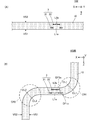
- FIG. 1A is a perspective view of the inductor bridge 101 according to the first embodiment
- FIG. 1B is an exploded perspective view of the inductor bridge 101
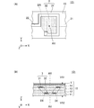
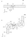
- 2A is a plan view showing a portion of the inductor bridge 101 where the conical coil 3 is formed
- FIG. 2B is a cross-sectional view of that portion
- 3A is a partial cross-sectional view of the inductor bridge 101 before being bent
- FIG. 3B is a partial cross-sectional view of the inductor bridge 101 after being bent.
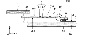
- FIG. 4 is a cross-sectional view showing the main part of the electronic apparatus 301 according to the first embodiment.
- FIG. 5 is a cross-sectional view sequentially illustrating manufacturing steps of the inductor bridge 101A.
- FIG. 6 is a cross-sectional view illustrating a main part of an electronic device 302 according to the second embodiment.
- FIG. 7A is a partial cross-sectional view of the inductor bridge 102 before bending
- FIG. 7B is a partial cross-sectional view of the inductor bridge 102 after bending.
- FIG. 8A is a partial cross-sectional view of another inductor bridge 102 according to the second embodiment before bending
- FIG. 8B is a partial cross-sectional view of the inductor bridge 102A after bending.
- FIG. 9A is a partial cross-sectional view of another inductor bridge 102 according to the second embodiment before bending
- FIG. 9A is a partial cross-sectional view of another inductor bridge 102 according to the second embodiment before bending
- FIG. 9A is a partial cross-sectional view of another inductor bridge 102 according to the second embodiment before bending
- FIG. 9A is a partial cross-sectional view of another inductor
- FIG. 9B is a partial cross-sectional view of the inductor bridge 102B after bending.
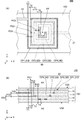
- FIG. 10A is a partial cross-sectional view of another inductor bridge 102 according to the second embodiment before being bent, and FIG. 10B is a partial cross-sectional view of the inductor bridge 102C after being bent. is there.
- FIG. 11A is a perspective view of the inductor bridge 103 according to the third embodiment, and FIG. 11B is an exploded perspective view of the inductor bridge 103.
- FIG. 12A is a plan view showing a portion of the inductor bridge 103 where the conical coil 3A is formed, and FIG. 11B is a cross-sectional view of that portion.
- FIG. 12A is a plan view showing a portion of the inductor bridge 103 where the conical coil 3A is formed
- FIG. 11B is a cross-sectional view of that portion.
- FIG. 13A is a plan view showing a portion of the inductor bridge 104 according to the fourth embodiment where the conical coil 3B is formed, and FIG. 13B is a cross-sectional view of that portion.
- FIG. 14A is a plan view showing a portion of the inductor bridge 105 according to the fifth embodiment where the conical coil 3C is formed, and FIG. 14B is a cross-sectional view of that portion.
- FIG. 15A is a plan view showing a portion of the inductor bridge 106 according to the sixth embodiment where the conical coil 3D is formed, and FIG. 15B is a cross-sectional view of that portion.
- FIG. 14A is a plan view showing a portion of the inductor bridge 106 according to the sixth embodiment where the conical coil 3D is formed
- FIG. 15B is a cross-sectional view of that portion.
- FIG. 16A is a plan view showing each loop-shaped conductor of a portion where the conical coil 3E of the inductor bridge 107 according to the seventh embodiment is formed, and FIG. 16B is each coil portion of that portion.
- FIG. FIG. 17 is a cross-sectional view of a portion of the inductor bridge 107 where the conical coil 3E is formed.
- FIG. 18 is an exploded perspective view of one inductor bridge disclosed in Patent Document 1. In FIG.
- FIG. 1A is a perspective view of the inductor bridge 101 according to the first embodiment
- FIG. 1B is an exploded perspective view of the inductor bridge 101
- 2A is a plan view showing a portion of the inductor bridge 101 where the conical coil 3 is formed
- FIG. 2B is a cross-sectional view of that portion.
- the protective layer 1 and the base material layer 14 are not shown in order to make the structure easy to understand.
- the opening BR surrounded by the large-diameter loop conductor 31 is indicated by a dot pattern.
- the inductor bridge 101 includes an insulating base material 10, a protective layer 1, a conical coil 3 (described later in detail) formed on the insulating base material 10, and connectors 51 and 52.
- the insulating substrate 10 is a rectangular parallelepiped thermoplastic resin flat plate having a first main surface VS1 and a second main surface VS2 facing the first main surface VS1, and having a longitudinal direction coinciding with the X-axis direction.
- the insulating base material 10 is a laminate formed by laminating the base material layers 11, 12, 13, 14 and the protective layer 1, and has flexibility.
- the plurality of base material layers 11, 12, 13, and 14 are sheet-like flat plates made of a thermoplastic resin whose main material is a liquid crystal polymer, for example, whose planar shape is rectangular, the longitudinal direction of which coincides with the X-axis direction. .
- the electrode 41 is formed on the back surface of the base material layer 11.
- the electrode 41 is a conductor pattern having a rectangular planar shape disposed near the first end of the base material layer 11 (the right end of the base material layer 11 in FIG. 1B).
- the electrode 41 is a conductor pattern such as a Cu foil.
- a small-diameter loop conductor 32 and a conductor 21 are formed on the back surface of the base material layer 12.
- the small-diameter loop conductor 32 is a rectangular loop conductor pattern of about 0.7 turns formed near the center of the base material layer 12.
- the conductor 21 is a linear conductor pattern extending in the X-axis direction, and is disposed at a position near the first end of the base material layer 12 from the vicinity of the center of the base material layer 12.
- the small-diameter loop conductor 32 and the conductor 21 are continuously formed, and the first end of the small-diameter loop conductor 32 is connected to the first end of the conductor 21.
- a second end of the conductor 21 is connected to the electrode 41 via an interlayer connection conductor V ⁇ b> 1 formed on the base material layer 11.
- the small-diameter loop conductor 32 and the conductor 21 are conductor patterns such as Cu foil, and the interlayer connection conductor V1 is a via conductor or a through hole, for example.
- a large-diameter loop conductor 31 and a conductor 22 are formed on the surface of the base material layer 13.
- the large-diameter loop conductor 31 is a rectangular loop conductor pattern of about 0.8 turns formed near the center of the base material layer 13. As shown in FIG. 2A, the large-diameter loop conductor 31 has a larger inner and outer diameter than the small-diameter loop conductor 32.
- the conductor 22 is a linear conductor pattern extending in the X-axis direction, and is closer to the second end of the base material layer 13 (the left end of the base material layer 13 in FIG. 1B) from near the center of the base material layer 13. Placed in position.
- the first end of the large-diameter loop conductor 31 is connected to the small-diameter loop conductor 32 via an interlayer connection conductor V2 formed on the base material layers 12 and 13.
- the large-diameter loop conductor 31 and the conductor 22 are formed continuously, and the second end of the large-diameter loop conductor 31 is connected to the first end of the conductor 22.
- the large-diameter loop conductor 31 and the conductor 22 are conductor patterns such as Cu foil, and the interlayer connection conductor V2 is a via conductor or a through hole, for example.
- the “large-diameter loop conductor” in the present invention refers to a loop-shaped conductor having the largest inner and outer diameters (inner diameter and outer diameter) among a plurality of loop conductors constituting the conical coil.
- the electrode 42 is formed on the surface of the base material layer 14.
- the electrode 42 is a conductor pattern having a rectangular planar shape disposed near the second end of the base material layer 14 (the left end of the base material layer 14 in FIG. 1B).
- the electrode 42 is connected to the second end of the conductor 22 via an interlayer connection conductor V3 formed on the base material layer 14.
- the electrode 42 is a conductor pattern such as a Cu foil, and the interlayer connection conductor V3 is a via conductor or a through hole, for example.
- the protective layer 1 has substantially the same planar shape as the base material layer 14 and is laminated on the surface of the base material layer 14.
- the protective layer 1 has an opening AP1 corresponding to the position of the electrode 42. Therefore, the electrode 42 is exposed to the first main surface VS1 of the insulating base material 10.
- the protective layer 1 is, for example, a solder resist film.
- the protective layer 1 is not essential.
- the connector 51 is provided on the second main surface VS2 of the insulating base material 10, and is disposed at the first end in the longitudinal direction of the insulating base material 10 (the right end of the insulating base material 10 in FIG. 1A).
- the connector 51 is connected to the electrode 41.
- the connector 52 is provided on the first main surface VS ⁇ b> 1 of the insulating base 10 and is disposed at the second end in the longitudinal direction of the insulating base 10 (the left end of the insulating base 10).
- the connector 52 is connected to the electrode 42.
- the rectangular conical coil 3 of about 1.5 turns is configured including the small-diameter loop conductor 32, the large-diameter loop conductor 31 and the interlayer connection conductor V2 formed on the plurality of base material layers 12 and 13, respectively. Is done.
- the conical coil 3 has a winding axis AX orthogonal to the first main surface VS1 and the second main surface VS2 (parallel to the Z-axis direction).
- the plurality of loop conductors are arranged along the winding axis AX direction (Z-axis direction) of the conical coil 3.
- the large-diameter loop conductor 31 having the largest inner / outer diameter among the plurality of loop-shaped conductors is another loop shape in the winding axis AX direction (Z-axis direction) of the conical coil 3. It is arranged closer to the first main surface VS1 than the conductor (small-diameter loop conductor 32).
- the change in the Z-axis direction of the inner and outer diameters of the plurality of loop-shaped conductors is one direction (see the outline DE of the conical coil 3 in FIG. 2B).
- “the change along the winding axis direction is one direction” means that the inner and outer diameters of the plurality of loop-shaped conductors change so as to increase (or decrease) along the Z-axis direction.
- the large-diameter loop conductor 31 is disposed closer to the first main surface VS1 than the other loop-shaped conductors (small-diameter loop-shaped conductor 32) in the Z-axis direction.
- the small-diameter loop conductor 32 having the smallest diameter is disposed at a position farthest from the first main surface VS1 in the Z-axis direction as compared with other loop conductors (large-diameter loop conductor 31). That is, as shown in the outline DE of the conical coil 3 in FIG. 2B, the inner and outer diameters of the plurality of loop-shaped conductors are directed in the + Z direction (from the second main surface VS2 side to the first main surface VS1 side). It has changed to become larger.
- the small-diameter loop conductor 32 is disposed inside the opening BR surrounded by the large-diameter loop conductor 31 when viewed from the Z-axis direction. Further, the plurality of loop conductors (the large-diameter loop conductor 31 and the small-diameter loop conductor 32) do not overlap each other when viewed from the Z-axis direction.
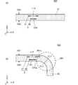
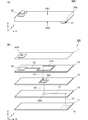
- FIG. 3A is a partial cross-sectional view of the inductor bridge 101 before bending
- FIG. 3B is a partial cross-sectional view of the inductor bridge 101 after bending.
- the inductor bridge 101 is bent in an L shape (with the second main surface VS2 on the inside) along the longitudinal direction (X-axis direction) of the insulating base 10.
- the first main surface VS1 side is deformed to be pulled by the bending displacement of the insulating base material 10, and the second main surface VS2 side is deformed to be compressed.
- the large-diameter loop-shaped conductor 31 located closer to the first main surface VS1 in the Z-axis direction extends toward both ends in the longitudinal direction of the insulating base 10. Displacement (see hollow arrow DF1 in FIG. 3B).
- the small-diameter loop conductor 32 positioned closer to the second main surface VS2 in the Z-axis direction is displaced so as to be contracted (a hollow arrow in FIG. 3B). See DF2.
- the large-diameter loop-shaped conductor 31 has an inner and outer diameter that is smaller than that of other loop-shaped conductors (small-diameter loop-shaped conductor 32) when the inductor bridge 101 is bent. Is disposed at a position (position near the first main surface VS1) that relatively expands along the insulating base 10. More specifically, the large-diameter loop conductor 31 has an inner diameter (L1b) of the large-diameter loop conductor 31 after the inductor bridge 101 is bent, and the large-diameter loop conductor 31 before the inductor bridge 101 is bent. It arrange
- the large-diameter loop conductor 31 and the other loop-shaped conductor may overlap when viewed from the Z-axis direction. No (they do not face each other). Therefore, the amount of change in the interlayer capacitance between the large-diameter loop conductor 31 and the other loop-shaped conductor (small-diameter loop conductor 32) is small.
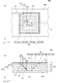
- FIG. 4 is a cross-sectional view showing the main part of the electronic apparatus 301 according to the first embodiment.
- the electronic device 301 includes an inductor bridge 101A, a circuit board 71, and a mounting board 201.
- the circuit configured on the circuit board 71 corresponds to the “first circuit” in the present invention
- the circuit configured on the mounting board 201 corresponds to the “second circuit” in the present invention.
- the inductor bridge 101A differs from the inductor bridge 101 in that the insulating base 10 includes a bent portion CR (bent portion) in part, and the other configurations are substantially the same.
- the inductor bridge 101A is connected to the circuit board 71 and the mounting board 201.
- a conductor 81 is formed on the upper surface of the mounting substrate 201.
- the receptacle 61 is connected to the conductor 81 and is electrically connected to a second circuit configured on the mounting substrate 201.
- the mounting substrate 201 is, for example, a printed wiring board.
- a receptacle 62 is mounted on the lower surface of the circuit board 71.
- the receptacle 62 is electrically connected to a first circuit formed on the circuit board 71.
- the first circuit is, for example, a radiating element of a UHF band antenna.
- the connector 51 is connected to the receptacle 61, and the connector 52 is connected to the receptacle 62.
- FIG. 5 is a cross-sectional view sequentially illustrating manufacturing steps of the inductor bridge 101A.
- a laminated body is formed by laminating a base layer patterned with small-diameter loop conductors, large-diameter loop conductors, conductors, electrodes, etc., and after coating the protective layer, the insulating base material from the aggregate substrate state Individual element bodies are separated to obtain an inductor bridge 101 shown in (1) in FIG.
- the first main surface VS1 and the second main surface of the insulating base 10 are formed along the Z-axis direction using the upper mold 5 and the lower mold 6.
- VS2 is heated and pressurized (see the arrow indicated by (2) in FIG. 5).
- the position to be heated and pressed is a position closer to the first end (the right end of the insulating base material) from the center in the longitudinal direction (X-axis direction) of the insulating base material 10.
- the upper mold 5 and the lower mold 6 have a structure in which a cross-sectional shape is bent into a predetermined shape.
- the inductor bridge 101A is taken out from the upper mold 5 and the lower mold 6.
- an inductor bridge 101A having a bent portion CR (bent portion) is obtained.
- the inductor bridges 101 and 101A according to the present embodiment have the following effects.
- a plurality of loop conductors (large-diameter loop conductor 31 and small-diameter loop conductor 32) having different inner and outer diameters are arranged along the Z-axis direction. Further, the large-diameter loop-shaped conductor 31 does not overlap other loop-shaped conductors (small-diameter loop-shaped conductor 32) when viewed from the Z-axis direction. With this configuration, the loop-shaped conductors (the large-diameter loop-shaped conductor 31 and the small-diameter loop-shaped conductor 32) do not face each other, so that the interlayer capacitance between the multiple loop-shaped conductors is small.
- another loop-shaped conductor (small-diameter loop-shaped conductor 32) is disposed inside the opening BR surrounded by the large-diameter loop-shaped conductor 31 when viewed from the Z-axis direction, and the large-diameter loop
- the conductor 31 and other loop conductors do not overlap each other when viewed from the Z-axis direction.
- the large-diameter loop conductor 31 is disposed at a position where the inner and outer diameters relatively expand along the insulating base material 10 as compared with other loop-shaped conductors when the inductor bridge 101 is bent.
- the plurality of loop conductors (the large diameter loop conductor 31 and the small diameter loop conductor 32) are face to face. Since it does not oppose, the change of the interlayer capacity
- the large-diameter loop conductor 31 when the inductor bridge 101 is bent, the large-diameter loop conductor 31 has a position where the inner and outer diameters extend along the insulating base material 10 (the first main surface rather than the neutral surface of the insulating base material 10).
- the other main conductor VS2 is located at a position where the inner and outer diameters of the other loop conductors (small-diameter loop conductors 32) contract along the insulating base material 10 (the neutral surface of the insulating base material 10 than the neutral surface).
- the large-diameter Both the loop-shaped conductor 31 and the other loop-shaped conductors may be arranged at a position where the inner and outer diameters expand (position closer to the first main surface VS1 than the neutral surface of the insulating base material 10).
- the large-diameter loop-shaped conductor 31 when the inductor bridge 101 is bent, if the inner and outer diameters of the large-diameter loop-shaped conductor 31 are arranged at a position that expands “relatively” compared to other loop-shaped conductors, the large-diameter loop-shaped conductor 31 All of the other loop-shaped conductors may be arranged at positions where the inner and outer diameters are reduced (positions closer to the second main surface VS2 than the neutral surface of the insulating base material 10). Further, when the inductor bridge 101 is bent, the large-diameter loop conductor 31 is arranged so that the inner and outer diameters of the large-diameter loop conductor 31 expand “relatively” compared to other loop-shaped conductors. Any of the other loop-shaped conductors may be disposed on the neutral surface of the insulating substrate 10. This is the same in the embodiments described below.
- the conical coil 3 is configured including the small-diameter loop conductor 32 and the large-diameter loop conductor 31 respectively formed on the plurality of base material layers 12 and 13. With this configuration, a conical coil having a predetermined number of turns and inductance can be formed on the insulating substrate 10.
- the insulating base material 10 is a thermoplastic resin, as shown to (2) in FIG. 5, a shape is easy according to a mounting state (unevenness
- Second Embodiment a structure different from the electronic device shown in the first embodiment will be described.
- FIG. 6 is a cross-sectional view showing the main part of the electronic device 302 according to the second embodiment.
- the electronic device 302 includes an inductor bridge 102, a resin casing 91, and a mounting substrate 202.
- a conductor pattern 4 is formed on the inner surface of the resin casing 91.
- the conductor pattern 4 is, for example, a ground conductor.
- the circuit configured on the mounting substrate 202 corresponds to the “first circuit” in the present invention
- the circuit (ground conductor) configured in the resin casing 91 corresponds to the “second circuit” in the present invention. To do.
- the inductor bridge 102 is connected to the conductor pattern 4 of the resin casing 91 and the conductor 82 of the mounting substrate 202.
- the inductor bridge 102 differs from the inductor bridge 101 in that a part thereof is bent.
- Other configurations are substantially the same as those of the inductor bridge 101.
- a conductor 82 is formed on the upper surface of the mounting substrate 202, and a conductor 83 is formed inside the mounting substrate 202.
- the receptacle 62 is connected to the conductor 82 and is electrically connected to a first circuit configured on the mounting substrate 202.
- the mounting board 202 is, for example, a printed wiring board.
- a receptacle 61 is mounted on the inner surface of the resin casing 91.
- the receptacle 61 is electrically connected to the conductor pattern 4 (ground conductor) formed inside the resin casing 91.
- the connector 51 of the inductor bridge 102 is connected to the receptacle 61, and the connector 52 is connected to the receptacle 62.
- the portion where the conical coil 3 is formed is exposed from the opening OP ⁇ b> 1 formed in the resin casing 91. Therefore, the conical coil 3 is not shielded from the electromagnetic field. Therefore, this inductor bridge 102 can be used as an antenna, and communication with the outside becomes possible.
- the inductor bridge 102 is connected to the mounting substrate 202 and the conductor pattern 4 of the resin casing 91, and the second end from the center in the longitudinal direction of the insulating base 10 (the right end of the insulating base 10 in FIG. 6). The close position is bent. Specifically, as shown in FIG. 6, the inductor bridge 102 is bent in an L shape at a portion where the conical coil 3 is not formed.
- FIG. 7A is a partial cross-sectional view of the inductor bridge 102 before bending
- FIG. 7B is a partial cross-sectional view of the inductor bridge 102 after bending.
- the inductor bridge 102 has a bent portion CR1 bent in an L shape.
- the conical coil 3 is located near the left side of the bent portion CR1.
- stress is applied in the + X direction on the first main surface VS1 side and stress is applied in the ⁇ X direction on the second main surface VS2 side as the insulating base material 10 is bent. Therefore, the large-diameter loop conductor 31 positioned closer to the first main surface VS1 in the Z-axis direction is displaced so that its inner and outer diameters are expanded (see the hollow arrow DF1c in FIG. 7B).
- the other loop-shaped conductor (small-diameter loop-shaped conductor 32) positioned closer to the second main surface VS2 in the Z-axis direction is displaced so that the inner and outer diameters thereof are reduced (see the hollow arrow DF2c in FIG. 7B). ). That is, the large-diameter loop conductor 31 has an inner diameter (L1c) of the large-diameter loop conductor 31 after the inductor bridge 102 is bent, and an inner diameter (L1a) of the large-diameter loop conductor 31 before the inductor bridge 102 is bent. It can be said that it is arranged at a position (L1a ⁇ L1c) that is larger than that.
- the large-diameter loop conductor 31 and the other loop-shaped conductor do not overlap when viewed from the Z-axis direction.
- the amount of change in the interlayer capacitance between the radial loop conductor 31 and the other loop conductor is small.
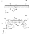
- FIG. 8A is a partial cross-sectional view of another inductor bridge 102 according to the second embodiment before bending
- FIG. 8B is a partial cross-sectional view of the inductor bridge 102A after bending.
- the inductor bridge 102A is different from the inductor bridge 102 in that the entire insulating base material 10 is bent in a U shape along the longitudinal direction (X-axis direction), and the other configuration is the same as that of the inductor bridge 102.
- the bent portions CR1 and CR2 are both bent in an L shape with the second main surface VS2 inside.
- the conical coil 3 is disposed between the bent portion CR1 and the bent portion CR2.
- the large-diameter loop-shaped conductor 31 has a large diameter before bending the inductor bridge 102A so that the inner diameter (L1d) of the large-diameter loop-shaped conductor 31 after bending like the inductor bridge 102A shown in FIG.
- the loop conductor 31 is disposed at a position (L1a ⁇ L1d) that is larger than the inner diameter (L1a) of the loop-shaped conductor 31.
- the inductor bridge 102A is bent as shown in FIG. 8B, the large-diameter loop-shaped conductor 31 and other loop-shaped conductors do not overlap when viewed from the Z-axis direction.
- the amount of change in the interlayer capacitance between the radial loop conductor 31 and the other loop conductor is small.
- FIG. 9A is a partial cross-sectional view of the inductor bridge 102 according to the second embodiment before being bent
- FIG. 9B is a partial cross-sectional view of the inductor bridge 102B after being bent
- FIG. 10A is a partial cross-sectional view of the inductor bridge 102 according to the second embodiment before being bent
- FIG. 10B is a partial cross-sectional view of the inductor bridge 102C after being bent.
- the inductor bridges 102B and 102C differ from the inductor bridge 102 in that the insulating base material 10 is bent in a Z shape along the longitudinal direction (X-axis direction), and the other configurations are the same as the inductor bridge 102.
- the bent portion CR1 is bent in an L shape with the second main surface VS2 inside, and the bent portion CR2 is the first main portion. It is bent in an L shape with the surface VS1 on the inside.
- the amount of deformation of the insulating base material when the inductor bridge is bent depends on the distance from the center line of the adjacent bent portion (the line at the intermediate position between the start point and the end point of the bent portion).
- the conical coil 3 is disposed closer to the center line CL1 than the center line CL2.
- the large-diameter loop-shaped conductor 31 has a large diameter before bending the inductor bridge 102B so that the inner diameter (L1e) of the large-diameter loop-shaped conductor 31 after bending as in the inductor bridge 102B shown in FIG.
- the loop conductor 31 is disposed at a position (L1a ⁇ L1e) which is larger than the inner diameter (L1a) of the loop conductor 31.
- the conical coil 3 is disposed between the bent portion CR1 and the bent portion CR2 and at a position near the bent portion CR2.
- the amount of deformation of the insulating base material when the inductor bridge is bent depends on the distance from the center line of the adjacent bent portion (the line at the intermediate position between the start point and the end point of the bent portion).
- the conical coil 3 is disposed closer to the center line CL2 than the center line CL1.
- the first main surface VS1 side is mainly stressed in the ⁇ X direction
- the second main surface VS2 side is mainly stressed in the + X direction. Therefore, the large-diameter loop conductor 31 positioned closer to the first main surface VS1 in the Z-axis direction is displaced so that its inner and outer diameters are expanded (see the hollow arrow DF1f in FIG. 10B). Further, the other loop-shaped conductor (small-diameter loop-shaped conductor 32) positioned closer to the second main surface VS2 in the Z-axis direction is displaced so that the inner and outer diameters are reduced (see the hollow arrow DF2f in FIG. 10B). ).
- the large-diameter loop-shaped conductor 31 has a large diameter before bending the inductor bridge 102C so that the inner diameter (L1f) of the large-diameter loop-shaped conductor 31 after bending like the inductor bridge 102C shown in FIG.
- the loop conductor 31 is disposed at a position (L1a ⁇ L1f) that is larger than the inner diameter (L1a) of the loop conductor 31.
- the inductor bridge 102 is connected to the conductor pattern 4 formed on the inner surface of the resin casing 91 via the receptacle 61 is shown, but the present invention is not limited to this configuration.
- the inductor bridge may be connected to the metal casing by screwing or the like.
- FIG. 11A is a perspective view of the inductor bridge 103 according to the third embodiment
- FIG. 11B is an exploded perspective view of the inductor bridge 103
- FIG. 12A is a plan view showing a portion of the inductor bridge 103 where the conical coil 3A is formed
- FIG. 11B is a cross-sectional view of that portion.
- the protective layer 1 and the base material layer 14 are not shown, the large-diameter loop conductor 31A is indicated by hatching, and the small-diameter loop conductor 32A is indicated by a dot pattern. Yes.
- the inductor bridge 103 includes an insulating base 10A, a conical coil 3A (described in detail later) formed on the insulating base 10A, and connectors 51 and 52.
- the insulating base material 10A is a rectangular parallelepiped thermoplastic resin flat plate having a first main surface VS1 and a second main surface VS2 facing the first main surface VS1, and having a longitudinal direction coinciding with the X-axis direction.
- the insulating base material 10A is a laminate formed by laminating the base material layers 11, 12, 13, and 14 and the protective layer 1, and has flexibility.
- the electrode 41 is formed on the back surface of the base material layer 11.
- the electrode 41 is a conductor pattern having a rectangular planar shape disposed near the first end of the base material layer 11 (the right end of the base material layer 11 in FIG. 11B).
- a small-diameter loop conductor 33A and a conductor 21 are formed on the back surface of the base material layer 12.
- the small-diameter loop-shaped conductor 33A is a rectangular loop-shaped conductor pattern having a strength of about 0.7 turns formed near the center of the base material layer 12.
- the conductor 21 is a linear conductor pattern extending in the X-axis direction, and is disposed at a position near the first end of the base material layer 12 from the vicinity of the center of the base material layer 12.
- the small-diameter loop conductor 33A and the conductor 21 are formed continuously, and the first end of the small-diameter loop conductor 33A is connected to the first end of the conductor 21.
- a second end of the conductor 21 is connected to the electrode 41 via an interlayer connection conductor V ⁇ b> 1 formed on the base material layer 11.
- a small-diameter loop conductor 32A is formed on the surface of the base material layer 13.
- the small-diameter loop conductor 32 ⁇ / b> A is a rectangular loop-shaped conductor pattern of about one turn formed near the center of the base material layer 13.
- the small-diameter loop conductor 32A has a larger inner and outer diameter than the small-diameter loop conductor 33A.
- a first end of the small-diameter loop conductor 32A is connected to a second end of the small-diameter loop conductor 33A via an interlayer connection conductor V2 formed on the base material layers 12 and 13, respectively.
- the large-diameter loop conductor 31A, the conductor 22, and the electrode 42 are formed on the surface of the base material layer 14.
- the large-diameter loop conductor 31 ⁇ / b> A is a rectangular loop-shaped conductor pattern of about 0.8 turns formed near the center of the base material layer 14.
- the large-diameter loop conductor 31A has a larger inner and outer diameter than the small-diameter loop conductors 32A and 33A.
- the conductor 22 is a linear conductor pattern extending in the X-axis direction, and is close to the second end of the base material layer 14 (the left end of the base material layer 14 in FIG. 11B) from the vicinity of the center of the base material layer 14. Placed in position.
- the electrode 42 is a conductor pattern having a rectangular planar shape disposed near the second end of the base material layer 14 (the left end of the base material layer 14 in FIG. 11B).
- the first end of the large-diameter loop conductor 31A is connected to the second end of the small-diameter loop conductor 32A via an interlayer connection conductor V3 formed in the base material layer 14.
- the second end of the large-diameter loop conductor 31 ⁇ / b> A is connected to the first end of the conductor 22, and the second end of the conductor 22 is connected to the electrode 42.
- the protective layer 1 has substantially the same planar shape as the base material layer 14 and is laminated on the surface of the base material layer 14.
- the protective layer 1 has an opening AP1 corresponding to the position of the electrode 42. Therefore, when the protective layer 1 is laminated on the surface of the base material layer 14, the electrode 42 is exposed to the first main surface VS1 of the insulating base material 10A.
- the connector 51 is provided on the second main surface VS2 of the insulating base 10A, and is arranged at the first end in the longitudinal direction of the insulating base 10A (the right end of the insulating base 10A in FIG. 11A).
- the connector 51 is connected to the electrode 41.
- the connector 52 is provided on the first main surface VS1 of the insulating base 10A, and is disposed at the second end in the longitudinal direction of the insulating base 10A (the left end of the insulating base 10A).
- the connector 52 is connected to the electrode 42.
- Inductor bridge 103 includes a large-diameter loop conductor 31A, small-diameter loop conductors 32A and 33A, and interlayer connection conductors V1 and V2 formed on a plurality of base material layers 12, 13, and 14, respectively, and takes about 2.5 turns.
- a rectangular conical coil 3A is formed. As shown in FIG. 12B, the conical coil 3A has a winding axis AX orthogonal to the first main surface VS1 and the second main surface VS2 (parallel to the Z-axis direction).
- the small-diameter loop conductors 32A and 33A are arranged inside the opening surrounded by the large-diameter loop conductor 31A when viewed from the Z-axis direction.
- the change along the Z-axis direction of the inner and outer diameters of the plurality of loop-shaped conductors is one direction.
- the inner and outer diameters of the plurality of loop conductors are in the + Z direction (from the second main surface VS2 side to the first main surface). It changes so as to increase toward the VS1 side.
- the present invention there may be a plurality of “other loop conductors” (loop conductors other than the large-diameter loop conductor) in the present invention. Even in this case, it is a condition that the plurality of loop conductors (large-diameter loop conductor 31A, small-diameter loop conductors 32A, 33A) do not overlap each other when viewed from the Z-axis direction.
- the small-diameter loop conductor 32A is disposed inside the opening surrounded by the large-diameter loop conductor 31A
- the small-diameter loop conductor 33A is disposed inside the opening surrounded by the small-diameter loop conductor 32A. Has been.
- the inner and outer diameters of the plurality of loop-shaped conductors are not limited to those that change uniformly along the Z-axis direction. That is, the inner and outer diameters of the plurality of loop-shaped conductors are not limited to those that change in one direction in proportion to the movement distance in the Z-axis direction.
- the inner and outer diameters of four loop-shaped conductors (including a large-diameter loop-shaped conductor) in the + Z direction (from the second main surface side to the first main surface side) are 2X ⁇ 4X ⁇ 5X ⁇ 8X (X is an arbitrary value)
- the configuration arranged along the Z-axis direction so as to be in the order of (number) is also included in the “change along the winding axis direction is one direction” in the present invention. In this case, it is a condition that the four loop-shaped conductors do not overlap each other when viewed from the Z-axis direction.
- the inner and outer diameters of the four loop-shaped conductors (including the large-diameter loop-shaped conductor) in the + Z direction are 2X ⁇ 5X ⁇ 3X ⁇ 4X (X is an arbitrary value)
- the configuration arranged along the Z-axis direction so as to be in the order of (number) is excluded from the “change along the winding axis direction is one direction” in the present invention.
- FIG. 13A is a plan view showing a portion of the inductor bridge 104 according to the fourth embodiment where the conical coil 3B is formed, and FIG. 13B is a cross-sectional view of that portion.
- the first coil portion CP1 is indicated by hatching
- the second coil portion CP2 is indicated by a dot pattern
- the fourth coil portion CP4 is indicated by cross hatching.
- the inductor bridge 104 includes an insulating base material 10B, a conical coil 3B (described in detail later) formed on the insulating base material 10B, and the like.
- the basic configuration of the insulating substrate 10B is substantially the same as the insulating substrate 10A according to the third embodiment.
- the conical coil 3B includes a large-diameter loop conductor 31B, a small-diameter loop conductor 32B, a small-diameter loop conductor 33B, a small-diameter loop conductor 34B, and an interlayer connection conductor (not shown).
- the conical coil 3B has a winding axis AX that is orthogonal to the first main surface VS1 and the second main surface VS2 (parallel to the Z-axis direction).
- the conical coil 3B is wound more than two turns (about 4.5 turns), and has a first coil part CP1, a second coil part CP2, a third coil part CP3, and a fourth coil part CP4.
- the first coil portion CP1 is a portion that winds the outermost periphery in the conical coil 3B when viewed from the Z-axis direction.
- the second coil portion CP2 is a portion that is first positioned toward the inner peripheral side with respect to the first coil portion CP1 when viewed from the Z-axis direction.
- the third coil part CP3 is a part that is secondly located toward the inner peripheral side with respect to the first coil part CP1.
- the fourth coil portion CP4 is a portion that is located third in the inner circumferential side with respect to the first coil portion CP1.
- the one-turn large-diameter loop conductor 31B formed on the surface of the base material layer 14 coincides with the first coil portion CP1
- the base material layer A one-turn small-diameter loop-shaped conductor 32B formed on the surface of 13 coincides with the second coil portion CP2.
- the one-turn small-diameter loop conductor 33B formed on the surface of the base material layer 12 coincides with the third coil portion CP3, and the.
- the five-turn small-diameter loop conductor 34B coincides with the fourth coil portion CP4.
- the line widths of the first coil portion CP1, the second coil portion CP2, the third coil portion CP3, and the fourth coil portion CP4 are equal to each other.
- the first coil part CP1, the second coil part CP2, the third coil part CP3, and the fourth coil part CP4 are arranged in this order.
- the overall length of the first coil portion CP1 is longer than the other coil portions, and the overall length of the fourth coil portion CP4 located on the innermost side is shorter than the other coil portions.
- the conical coil 3B has a first gap G1, a second gap G2, and a third gap G3.
- the first gap G1 is a gap between the first coil portion CP1 (large diameter loop conductor 31B) and the second coil portion CP2 (small diameter loop conductor 32B).
- the second gap G2 is a gap between the second coil part CP2 and the third coil part CP3 (small-diameter loop conductor 33B).
- the third gap G3 is a gap between the third coil portion CP3 and the fourth coil portion CP4 (small-diameter loop conductor 34B).
- the first gap G1 is larger than other gaps (the second gap G2 and the third gap G3) other than the first gap G1.
- the second gap G2 is larger than the third gap G3.
- the first gap VG1 in the Z-axis direction is equal to the other gaps (second gap VG2 and third gap VG3) in the Z-axis direction.
- the first gap PG1 viewed from the Z-axis direction is more than the other gaps (second gap PG2 and third gap PG3) viewed from the Z-axis direction. Is also big.
- the second gap PG2 viewed from the Z-axis direction is larger than the third gap PG3 viewed from the Z-axis direction. Therefore, as described above, the first gap G1 is larger than the other gaps (the second gap G2 and the third gap G3), and the second gap G2 is larger than the third gap G3.
- the inductor bridge 104 according to the present embodiment has the following effects in addition to the effects described in the third embodiment.
- the first gap G1 is larger than other gaps (the second gap G2 and the third gap G3) other than the first gap G1.
- the portions where the first coil portion CP1 and the second coil portion CP2 are running in parallel are the other coil portions (the second coil portion CP2 and the third coil portion CP3, or the third coil portion CP3 and the fourth coil).
- the part CP4) is longer than the parts running parallel to each other. Therefore, with this configuration, the line capacity of the conical coil 3B can be effectively reduced and the self-resonant frequency of the conical coil 3B can be increased, compared to increasing the other gaps (second gap G2 and third gap G3).
- the position of each loop-shaped conductor may be shifted due to the stacking error of the base material layers, and the line capacity of the entire conical coil may fluctuate.
- the portion where the first coil portion CP1 and the second coil portion CP2 run parallel to each other is longer than the portion where the other coil portions run parallel to each other.
- the proportion of the line capacitance generated between the first coil portion CP1 and the second coil portion CP2 is large with respect to the inter capacitance.
- the first gap G1 (the gap between the first coil portion CP1 and the second coil portion CP2) is larger than the other gaps, even if the position of each loop conductor is displaced, the conical coil Variation in line capacitance can be suppressed.
- the conical coil 3B can be effectively reduced in line capacitance as compared with the case where all the gaps (the first gap G1, the second gap G2, and the third gap G3) are made equally large.
- the increase in size of the coil 3B can be suppressed.
- the first gap PG1 viewed from the Z-axis direction is larger than the other gaps (second gap PG2 and third gap PG3) viewed from the Z-axis direction.
- the second gap G2 viewed from the Z-axis direction is larger than the third gap G3 viewed from the Z-axis direction. Therefore, compared with the case where the gaps (first gap PG1, second gap PG2, and third gap PG3) viewed from the Z-axis direction are all equally increased, the line capacitance of the conical coil 3B is effectively reduced, An increase in size of the conical coil 3B on the plane (XY plane) can be suppressed. That is, the above configuration is effective when it is desired to reduce the thickness of the conical coil in the Z-axis direction while reducing the line capacitance of the conical coil.
- the second gap G2 is larger than the third gap G3.
- the part where the second coil part CP2 and the third coil part CP3 run parallel to each other is longer than the part where the third coil part CP3 and the fourth coil part CP4 run parallel to each other. Therefore, with this configuration, the line capacity of the conical coil 3B can be effectively reduced and the self-resonant frequency of the conical coil 3B can be increased rather than increasing the third gap G3. That is, the line capacity of the conical coil can be effectively reduced by increasing the gap between the coil portions located on the outer peripheral side.
- the conical coil 3B having four coil parts (first coil part CP1, second coil part CP2, third coil part CP3, and fourth coil part CP4) is shown. Is not to be done.
- the “conical coil” of the present invention may have an n-th coil portion (n is an integer of 2 or more).
- the n-th coil portion refers to a portion located at the (n ⁇ 1) th position toward the inner peripheral side with respect to the first coil portion CP1 when viewed from the Z-axis direction.
- the conical coil 3B having three gaps (the first gap G1, the second gap G2, and the third gap G3) is shown, but the present invention is not limited to this configuration.
- the “conical coil” of the present invention may have an nth gap (n is an integer of 2 or more).
- the nth gap refers to the gap between the nth coil part and the (n + 1) th coil part.
- the first gap G1 is preferably larger than the other gaps.
- the nth gap is preferably larger than the (n + 1) th gap.
- FIG. 14A is a plan view showing a portion of the inductor bridge 105 according to the fifth embodiment where the conical coil 3C is formed, and FIG. 14B is a cross-sectional view of that portion.
- the first coil portion CP1 is indicated by hatching
- the second coil portion CP2 is indicated by a dot pattern
- the fourth coil portion CP4 is indicated by cross hatching.
- the inductor bridge 105 includes an insulating base material 10C, a conical coil 3C (described in detail later) formed on the insulating base material 10C, and the like.
- the basic configuration of the insulating substrate 10C is substantially the same as that of the insulating substrate 10B according to the fourth embodiment.
- the conical coil 3C includes a large-diameter loop conductor 31C, a small-diameter loop conductor 32C, a small-diameter loop conductor 33C, a small-diameter loop conductor 34C, and an interlayer connection conductor (not shown).
- the conical coil 3C has a winding axis AX that is orthogonal to the first main surface VS1 and the second main surface VS2 (parallel to the Z-axis direction).
- the conical coil 3C is wound more than two turns (about 4.5 turns) and has a first coil part CP1, a second coil part CP2, a third coil part CP3, and a fourth coil part CP4.
- the first coil portion CP1, the second coil portion CP2, the third coil portion CP3, and the fourth coil portion CP4 are substantially the same as those described in the fourth embodiment.
- the one-turn large-diameter loop conductor 31C formed on the surface of the base material layer 14 coincides with the first coil portion CP1
- a one-turn small-diameter loop conductor 32C formed on the back surface of the material layer 13 coincides with the second coil portion CP2.
- the one-turn small-diameter loop conductor 33C formed on the back surface of the base material layer 12 is aligned with the third coil portion CP3, and is formed on the back surface of the base material layer 11.
- the 5-turn small-diameter loop conductor 34C coincides with the fourth coil portion CP4.
- the line widths of the first coil portion CP1, the second coil portion CP2, the third coil portion CP3, and the fourth coil portion CP4 are equal to each other.
- the conical coil 3C has a first gap G1, a second gap G2, and a third gap G3. As shown in FIG. 14B, the first gap G1 is larger than other gaps (the second gap G2 and the third gap G3) other than the first gap G1. The second gap G2 is larger than the third gap G3.
- the first gap PG1 viewed from the Z-axis direction is equal to the other gaps (second gap PG2 and third gap PG3) viewed from the Z-axis direction.
- the first gap VG1 in the Z-axis direction is larger than the other gaps (second gap VG2 and third gap VG3) in the Z-axis direction.
- the second gap PG2 viewed from the Z-axis direction is larger than the third gap PG3 viewed from the Z-axis direction. Therefore, as described above, the first gap G1 is larger than the other gaps (the second gap G2 and the third gap G3), and the second gap G2 is larger than the third gap G3.
- the first gap VG1 in the Z-axis direction is larger than the other gaps (second gap VG2 and third gap VG3) in the Z-axis direction.
- the second gap VG2 is larger than the third gap VG3 in the Z-axis direction. That is, the nth gap in the Z-axis direction is larger than the n + 1th gap in the Z-axis direction.
- the above configuration is effective when it is desired to reduce the area of the conical coil (area on the XY plane of the conical coil) viewed from the Z-axis direction while reducing the line capacitance of the conical coil.
- FIG. 15A is a plan view showing a portion of the inductor bridge 106 according to the sixth embodiment where the conical coil 3D is formed, and FIG. 15B is a cross-sectional view of that portion.
- the first coil portion CP1 is indicated by hatching
- the second coil portion CP2 is indicated by a dot pattern
- the fourth coil portion CP4 is indicated by cross hatching.
- the inductor bridge 106 includes an insulating base 10D, a conical coil 3D (described in detail later) formed on the insulating base 10D, and the like.
- the basic configuration of the insulating base 10D is substantially the same as that of the insulating base 10B according to the fourth embodiment.
- the conical coil 3D includes a large-diameter loop conductor 31D, a small-diameter loop conductor 32D, a small-diameter loop conductor 33D, a small-diameter loop conductor 34D, and an interlayer connection conductor (not shown).
- the conical coil 3D has a winding axis AX orthogonal to the first main surface VS1 and the second main surface VS2 (parallel to the Z-axis direction).
- the conical coil 3D is wound more than two turns (about 4.5 turns), and has a first coil part CP1, a second coil part CP2, a third coil part CP3, and a fourth coil part CP4.
- the one-turn large-diameter loop conductor 31D formed on the surface of the base material layer 14 coincides with the first coil portion CP1, and the base material layer
- the one-turn small-diameter loop conductor 32D formed on the surface of 14 coincides with the second coil portion CP2.
- the one-turn small-diameter loop conductor 33D formed on the surface of the base material layer 12 is aligned with the third coil portion CP3 and is formed on the surface of the base material layer 11.
- a 5-turn small-diameter loop conductor 34D coincides with the fourth coil portion CP4.
- the line width of the first coil portion CP1 is the same as that of the other coil portions (the line width T2 of the second coil portion CP2 and the third coil portion CP3. It is narrower than the line width T3 and the line width T4) of the fourth coil portion CP4. Further, the line width of the nth coil part is narrower than the line width of the (n + 1) th coil part. Specifically, the line width T2 of the second coil part CP2 is narrower than the line width T3 of the third coil part CP3, and the line width T3 of the third coil part CP3 is smaller than the line width T4 of the fourth coil part CP4. Is also thin. When the line widths of the coil portions are arranged in order of narrowness, the first coil portion CP1, the second coil portion CP2, the third coil portion CP3, and the fourth coil portion CP4 are arranged in this order.
- the conical coil 3D has a first gap G1, a second gap G2, and a third gap G3. As shown in FIG. 15B, the first gap G1 is equal to other gaps (the second gap G2 and the third gap G3) other than the first gap G1.
- the first gap PG1 viewed from the Z-axis direction is equal to the other gaps (second gap PG2 and third gap PG3) viewed from the Z-axis direction.
- the first gap VG1 in the Z-axis direction is equal to the other gaps (second gap VG2 and third gap VG3) in the Z-axis direction. Therefore, as described above, the first gap G1 is equal to the other gaps (second gap G2 and third gap G3).
- the inductor bridge 106 according to this embodiment has the following effects in addition to the effects described in the third embodiment.
- the line width T1 of the first coil portion CP1 is equal to the line width of the other coil portions (the line width T2 of the second coil portion CP2, the line width T3 of the third coil portion CP3, and the fourth coil). It is narrower than the line width T4) of the part CP4.
- the portions where the first coil portion CP1 and the second coil portion CP2 are running in parallel are the other coil portions (the second coil portion CP2 and the third coil portion CP3, or the third coil portion CP3 and the fourth coil).
- the part CP4) is longer than the parts running parallel to each other.
- the opposing area between the first coil part CP1 and the second coil part CP2 is reduced, so that the line width of the other coil parts is reduced (the opposing area between the other coil parts is reduced). Rather, the line capacitance of the conical coil 3D can be effectively reduced, and the self-resonant frequency of the conical coil 3D can be increased.
- the conical coil linear capacitance without increasing the thickness of the conical coil in the Z-axis direction or the area of the conical coil viewed from the Z-axis direction (the area on the XY plane of the conical coil). Can be reduced.
- the DC resistance is reduced compared to the case where the line widths of all the coil portions (the first coil portion CP1, the second coil portion CP2, the third coil portion CP3, and the fourth coil portion CP4) are reduced.
- the line capacitance of the conical coil 3D can be effectively reduced.
- the line width T2 of the second coil portion CP2 is narrower than the third coil portion CP3T3, and the line width T3 of the third coil portion CP3 is equal to the line width T4 of the fourth coil portion CP4. Thinner than. That is, the line width of the nth coil part is narrower than the line width of the (n + 1) th coil part.
- the portion where the n-th coil portion and the n + 1-th coil portion run parallel to each other is longer than the portion where the n + 1-th coil portion and the n + 2-th coil portion run parallel to each other.
- the line capacitance of the conical coil 3D can be effectively reduced and the self-resonant frequency of the conical coil 3D can be increased, rather than reducing the line width of the (n + 1) th coil portion. That is, the line capacity of the conical coil can be effectively reduced by narrowing the line width of the coil portion located on the outer peripheral side.
- FIG. 16A is a plan view showing each loop-shaped conductor of a portion where the conical coil 3E of the inductor bridge 107 according to the seventh embodiment is formed, and FIG. 16B is each coil portion of that portion.
- FIG. FIG. 17 is a cross-sectional view of a portion of the inductor bridge 107 where the conical coil 3E is formed.
- the large-diameter loop conductor 31E is indicated by hatching
- the small-diameter loop conductor 32E is indicated by a dot pattern
- the small-diameter loop conductor 33E is indicated by cross-hatching.
- the first coil portion CP1 is indicated by hatching
- the second coil portion CP2 is indicated by a dot pattern
- the fourth coil portion CP4 is indicated by cross hatching.
- the inductor bridge 107 includes an insulating base material 10E, a conical coil 3E (described in detail later) formed on the insulating base material 10E, and the like.
- the basic configuration of the insulating base material 10E is substantially the same as that of the insulating base material 10A according to the third embodiment.
- the conical coil 3E includes a large-diameter loop conductor 31E, a small-diameter loop conductor 32E, a small-diameter loop conductor 33E, and an interlayer connection conductor (not shown). Note that the basic configuration of the conical coil 3E is substantially the same as the conical coil 3A described in the third embodiment.
- the conical coil 3E is wound more than 2 turns (about 2.5 turns), and has a first coil part CP1, a second coil part CP2, a third coil part CP3, and a fourth coil part CP4.
- the first coil portion CP1 includes a large-diameter loop conductor 31E formed on the surface of the base material layer 14, and the base material layer 13. And a part of a small-diameter loop-shaped conductor 32E formed on the surface.
- the second coil portion CP2 includes a part of the small-diameter loop conductor 32E formed on the surface of the base material layer 13 and a part of the small-diameter loop conductor 33E formed on the surface of the base material layer 12. It is configured.
- the third coil portion CP3 is constituted by a part of the small-diameter loop conductor 33E.
- the conical coil 3E has a first gap G1 and a second gap G2, as shown in FIG.
- the first gap G1 is larger than other gaps (second gap G2) other than the first gap G1.
- planar shape of an insulating base material is a rectangle
- the planar shape of the insulating substrate can be changed as appropriate within the scope of the effects and effects of the present invention, and may be, for example, a polygon, a circle, an ellipse, an L shape, a crank shape, a T shape, a Y shape, or the like. .
- an inductor bridge including an insulating base material formed by laminating four base material layers has been described.
- the present invention is not limited to this configuration.
- the number of base material layers forming the insulating base material can be appropriately changed within a range where the functions and effects of the present invention are exhibited.
- the base material layer may be a single layer.
- a conical coil of about 1.5 turns, 2.5 turns, or 4.5 turns is configured including loop-shaped conductors respectively formed on a plurality of base material layers.
- the number of turns of the conical coil provided in the inductor bridge can be changed as appropriate.
- the outer shape of the conical coil viewed from the winding axis direction (Z-axis direction) may be, for example, a circle, an ellipse, a rectangle, or a polygon.
- a conical coil including a small-diameter loop conductor and a large-diameter loop conductor of less than one turn has been shown, but a spiral small-diameter loop conductor and a large-diameter loop including one or more turns You may comprise a conical coil including a conductor.
- each embodiment shown above showed the example in which one connector was each provided in each surface of the 1st main surface and 2nd main surface of an insulation base material, it is not limited to this structure. Absent. The two connectors may be provided only on the first main surface of the insulating base material, or may be provided only on the second main surface. Further, the arrangement and number of connectors can be appropriately changed depending on the circuit configuration of the inductor bridge.
- the connector is not essential. You may connect a connection part to a 1st circuit, a 2nd circuit, etc. by electroconductive joining materials, such as solder, without using a connector.
- Opening portion AX ... Conical coil winding axis BR ... Opening portion surrounded by large-diameter loop conductor DE ... Conical coil outline CL1, CL2 ... Center line OP1 ... Opening CR, CR1, CR2 ... Bending portion CP1 ... 1st coil part CP2 ... 2nd coil part CP3 ... 3rd coil part CP4 ... 4th coil part G1 ... 1st gap G2 ... 2nd gap G3 ... 3rd gap PG1 ... 1st gap PG2 seen from a winding axis direction ... second gap PG3 viewed from the winding axis direction ... third gap VG1 viewed from the winding axis direction ...
- first gap VG2 in the winding axis direction ... second gap VG3 in the winding axis direction ... in the winding axis direction
- Body VS1 ... first main surface VS2 of insulating base material ... second main surface 1 of insulating base material ... protective layer 3, 3A, 3B, 3C, 3D ... conical coil 5 ... upper die 6 ...
Landscapes
- Engineering & Computer Science (AREA)
- Microelectronics & Electronic Packaging (AREA)
- Power Engineering (AREA)
- Manufacturing & Machinery (AREA)
- Coils Or Transformers For Communication (AREA)
- Structure Of Printed Boards (AREA)
- Parts Printed On Printed Circuit Boards (AREA)
Abstract
電子機器(301)は、第1回路(回路基板(71))、第2回路(実装基板(201)に構成された回路)、第1回路と第2回路とを接続するインダクタブリッジ(101A)を備える。インダクタブリッジ(101A)は、絶縁基材(10)、絶縁基材(10)に形成されるコニカルコイル(3)を有する。コニカルコイル(3)は、巻回軸方向(Z軸方向)に沿って配置される複数のループ状導体(小径ループ状導体(32)および大径ループ状導体(31))を含む。複数のループ状導体の内外径の、Z軸方向に沿った変化は一方向である。複数のループ状導体のうち内外径の最も大きな大径ループ状導体(31)は、インダクタブリッジ(101A)が屈曲したときに、内外径が他のループ状導体(小径ループ状導体(32))と比べて相対的に絶縁基材(10)に沿って拡がる位置に配置される。
Description
本発明は、電子機器に関し、特にインダクタンス成分を有するインダクタブリッジを備えた電子機器に関するものである。
従来、携帯端末等の小型電子機器において、筐体内に複数の基板等の実装回路部材を備える場合に、例えば特許文献1に示されているように、可撓性を有するフラットケーブルで実装回路部材間が接続される。
図18は、特許文献1に示されている一つのインダクタブリッジ100の分解斜視図である。このインダクタブリッジ100は、可撓性を有する絶縁基材(基材層11a,12a,13a,14aの積層体)と、絶縁基材に形成されるヘリカルコイル(ループ状導体31a,32a,33a,34aで構成されるヘリカル状のコイル)とを備えている。
特許文献1に示されるような可撓性を有するインダクタブリッジは、電子機器の内部の限られた空間に設けられる場合に、所定箇所が屈曲した状態で設けられることがある。ところが、インダクタブリッジが屈曲すると、絶縁基材の変形に伴ってヘリカルコイルの形状が変形し、ヘリカルコイルの線間容量(層間容量)が変化することがあり、インダクタブリッジの屈曲前後でヘリカルコイルの電気的特性が変化する場合がある。
本発明の目的は、屈曲に伴う電気的特性の変動を抑制したインダクタブリッジを備える電子機器を提供することにある。
(1)本発明の電子機器は、
インダクタブリッジと、第1回路と、第2回路と、を備え、
前記第1回路と前記第2回路とが前記インダクタブリッジを介して接続され、
前記インダクタブリッジは、
第1主面を有し、可撓性を有する絶縁基材と、
前記絶縁基材に形成され、前記第1主面に直交する巻回軸を有するコニカルコイルと、
を有し、
前記コニカルコイルは、前記コニカルコイルの巻回軸方向に沿って配置される複数のループ状導体を含んで構成され、
前記複数のループ状導体の内外径の、前記巻回軸方向に沿った変化は一方向であり、
前記複数のループ状導体は、前記巻回軸方向から視て、互いに重ならず、
前記複数のループ状導体のうち内外径の最も大きな大径ループ状導体は、前記インダクタブリッジが曲がったときに、内外径が他のループ状導体と比べて相対的に前記絶縁基材に沿って拡がる位置に配置されることを特徴とする。
インダクタブリッジと、第1回路と、第2回路と、を備え、
前記第1回路と前記第2回路とが前記インダクタブリッジを介して接続され、
前記インダクタブリッジは、
第1主面を有し、可撓性を有する絶縁基材と、
前記絶縁基材に形成され、前記第1主面に直交する巻回軸を有するコニカルコイルと、
を有し、
前記コニカルコイルは、前記コニカルコイルの巻回軸方向に沿って配置される複数のループ状導体を含んで構成され、
前記複数のループ状導体の内外径の、前記巻回軸方向に沿った変化は一方向であり、
前記複数のループ状導体は、前記巻回軸方向から視て、互いに重ならず、
前記複数のループ状導体のうち内外径の最も大きな大径ループ状導体は、前記インダクタブリッジが曲がったときに、内外径が他のループ状導体と比べて相対的に前記絶縁基材に沿って拡がる位置に配置されることを特徴とする。
この構成では、大径ループ状導体が、インダクタブリッジが屈曲したときに、内外径が他のループ状導体と比べて相対的に絶縁基材に沿って拡がる位置に配置されているため、大径ループ状導体と他のループ状導体とが面同士で対向しない。そのため、インダクタブリッジが屈曲しても、複数のループ状導体間の層間容量の変化が抑制され、インダクタブリッジの屈曲に伴うコニカルコイルの電気的特性の変動は抑制される。
(2)上記(1)において、前記絶縁基材は、熱可塑性樹脂からなる複数の基材層を積層して形成される積層体であることが好ましい。この構成では、絶縁基材が熱可塑性樹脂であるため、実装状態(実装先の凹凸等)に合わせて形状を容易に塑性加工できる。
(3)上記(1)または(2)において、前記インダクタブリッジは、一部に屈曲部を備えていてもよい。
(4)上記(1)から(3)のいずれかにおいて、前記コニカルコイルは、2ターンより多く巻回し、前記巻回軸方向から視て、前記コニカルコイルにおいて最も外周を巻回する部分を第1コイル部と定義し、前記第1コイル部に対して内周側に向かってn-1(nは2以上の整数)番目に位置する部分を第nコイル部と定義し、前記第1コイル部と第2コイル部との間隙を第1間隙と定義し、前記第nコイル部と第n+1コイル部との間隙を第n間隙と定義したとき、前記第1間隙はその他の間隙よりも大きいことが好ましい。第1コイル部と第2コイル部とが互いに並走している部分は、その他のコイル部同士が互いに並走している部分よりも長い。そのため、この構成により、その他の間隙を大きくするよりも、コニカルコイルの線間容量を効果的に低減でき、コニカルコイルの自己共振周波数を高くできる。
また、この構成により、全ての間隙を等しく大きくした場合と比べて、コニカルコイルの線間容量を効果的に低減しつつ、コニカルコイルの大型化を抑制できる。
(5)上記(4)において、前記第n間隙は、第n+1間隙よりも大きいことが好ましい。第nコイル部と第n+1とが互いに並走している部分は、第n+1コイル部と第n+2コイル部とが互いに並走している部分よりも長い。そのため、第n間隙を大きくすることにより、第n+1間隙を大きくするよりも、コニカルコイルの線間容量を効果的に低減でき、コニカルコイルの自己共振周波数を高くできる。
(6)上記(4)または(5)において、前記巻回軸方向から視た前記第1間隙は、前記巻回軸方向から視たその他の間隙よりも大きくてもよい。
(7)上記(6)において、前記巻回軸方向から視た前記第n間隙は、前記巻回軸方向から視た前記第n+1間隙よりも大きくてもよい。
(8)上記(4)から(7)のいずれかにおいて、前記巻回軸方向における前記第1間隙は、前記巻回軸方向におけるその他の間隙よりも大きくてもよい。
(9)上記(8)において、前記巻回軸方向における前記第n間隙は、前記巻回軸方向における第n+1間隔よりも大きくてもよい。
(10)上記(4)から(9)のいずれかにおいて、前記第1コイル部の線幅は、その他のコイル部の線幅よりも細いことが好ましい。第1コイル部と第2コイル部とが互いに並走している部分は、その他のコイル部同士が互いに並走している部分よりも長い。そのため、この構成により、第1コイル部と第2コイル部との対向面積が小さくなるため、その他のコイル部の線幅を細くするよりも(すなわち、その他のコイル部同士の対向面積を小さくするよりも)、コニカルコイルの線間容量を効果的に低減でき、コニカルコイルの自己共振周波数を高くできる。
(11)上記(10)において、前記第nコイル部の線幅は、前記第n+1コイル部の線幅よりも細いことが好ましい。第nコイル部と第n+1コイル部とが互いに並走している部分は、第n+1コイル部と第n+2コイル部とが互いに並走している部分よりも長い。そのため、この構成により、第n+1コイル部の線幅を細くするよりも、コニカルコイルの線間容量を効果的に低減でき、コニカルコイルの自己共振周波数を高くできる。
本発明によれば、屈曲に伴う電気的特性の変動を抑制したインダクタブリッジを備える電子機器を実現できる。
以降、図を参照して幾つかの具体的な例を挙げて、本発明を実施するための複数の形態を示す。各図中には同一箇所に同一符号を付している。要点の説明または理解の容易性を考慮して、便宜上実施形態を分けて示すが、異なる実施形態で示した構成の部分的な置換または組み合わせが可能である。第2の実施形態以降では第1の実施形態と共通の事柄についての記述を省略し、異なる点についてのみ説明する。特に、同様の構成による同様の作用効果については実施形態毎には逐次言及しない。
《第1の実施形態》
図1(A)は第1の実施形態に係るインダクタブリッジ101の斜視図であり、図1(B)はインダクタブリッジ101の分解斜視図である。図2(A)はインダクタブリッジ101のコニカルコイル3が形成された部分を示す平面図であり、図2(B)はその部分の断面図である。図2(A)では、構造を解りやすくするため、保護層1および基材層14の図示を省略している。また、図2(A)では、大径ループ状導体31で囲まれる開口部BRをドットパターンで示している。
図1(A)は第1の実施形態に係るインダクタブリッジ101の斜視図であり、図1(B)はインダクタブリッジ101の分解斜視図である。図2(A)はインダクタブリッジ101のコニカルコイル3が形成された部分を示す平面図であり、図2(B)はその部分の断面図である。図2(A)では、構造を解りやすくするため、保護層1および基材層14の図示を省略している。また、図2(A)では、大径ループ状導体31で囲まれる開口部BRをドットパターンで示している。
インダクタブリッジ101は、絶縁基材10、保護層1、絶縁基材10に形成されるコニカルコイル3(後に詳述する)、コネクタ51,52を備える。
絶縁基材10は、第1主面VS1および第1主面VS1に対向する第2主面VS2を有し、長手方向がX軸方向に一致する、直方体状の熱可塑性樹脂の平板である。
絶縁基材10は、基材層11,12,13,14および保護層1を積層して形成される積層体であり、可撓性を有する。複数の基材層11,12,13,14は、それぞれ長手方向がX軸方向に一致する、平面形状が矩形の、例えば液晶ポリマーを主材料とした熱可塑性樹脂からなるシート状の平板である。
基材層11の裏面には電極41が形成される。電極41は、基材層11の第1端(図1(B)における基材層11の右端)付近に配置される平面形状が矩形の導体パターンである。電極41は例えばCu箔等の導体パターンである。
基材層12の裏面には小径ループ状導体32および導体21が形成される。小径ループ状導体32は、基材層12の中央付近に形成される約0.7ターンの矩形ループ状の導体パターンである。導体21は、X軸方向に延伸する線状の導体パターンであり、基材層12の中央付近から基材層12の第1端寄りの位置に配置されている。小径ループ状導体32および導体21は連続形成されており、小径ループ状導体32の第1端は導体21の第1端に接続される。導体21の第2端は、基材層11に形成される層間接続導体V1を介して、電極41に接続される。小径ループ状導体32および導体21は例えばCu箔等の導体パターンであり、層間接続導体V1は例えばビア導体またはスルーホール等である。
基材層13の表面には、大径ループ状導体31および導体22が形成される。大径ループ状導体31は、基材層13の中央付近に形成される約0.8ターンの矩形ループ状の導体パターンである。図2(A)に示すように、大径ループ状導体31は、小径ループ状導体32よりも内外径が大きい。導体22は、X軸方向に延伸する線状の導体パターンであり、基材層13の中央付近から基材層13の第2端(図1(B)における基材層13の左端)寄りの位置に配置されている。大径ループ状導体31の第1端は、基材層12,13に形成される層間接続導体V2を介して、小径ループ状導体32に接続される。大径ループ状導体31および導体22は連続形成されており、大径ループ状導体31の第2端は導体22の第1端に接続される。大径ループ状導体31および導体22は例えばCu箔等の導体パターンであり、層間接続導体V2は例えばビア導体またはスルーホール等である。
なお、本発明における「大径ループ状導体」とは、コニカルコイルを構成する複数のループ状導体のうち最も内外径(内径および外径)の大きなループ状導体を言う。
基材層14の表面には電極42が形成される。電極42は、基材層14の第2端(図1(B)における基材層14の左端)付近に配置される、平面形状が矩形の導体パターンである。電極42は、基材層14に形成される層間接続導体V3を介して、導体22の第2端に接続される。電極42は例えばCu箔等の導体パターンであり、層間接続導体V3は例えばビア導体またはスルーホール等である。
保護層1は平面形状が基材層14と実質的に同一であり、基材層14の表面に積層される。保護層1は電極42の位置に応じた開口部AP1を有する。そのため、電極42は絶縁基材10の第1主面VS1に露出する。保護層1は例えばソルダーレジスト膜である。なお、保護層1は必須ではない。
コネクタ51は、絶縁基材10の第2主面VS2に設けられ、絶縁基材10の長手方向の第1端(図1(A)における絶縁基材10の右端)に配置される。コネクタ51は、電極41に接続される。コネクタ52は、絶縁基材10の第1主面VS1に設けられ、絶縁基材10の長手方向の第2端(絶縁基材10の左端)に配置される。コネクタ52は、電極42に接続される。
インダクタブリッジ101では、複数の基材層12,13にそれぞれ形成される小径ループ状導体32、大径ループ状導体31および層間接続導体V2を含んで約1.5ターンの矩形コニカルコイル3が構成される。図2(B)に示すように、コニカルコイル3は、第1主面VS1および第2主面VS2に直交する(Z軸方向に平行な)巻回軸AXを有する。
図2(B)に示すように、複数のループ状導体(小径ループ状導体32および大径ループ状導体31)は、コニカルコイル3の巻回軸AX方向(Z軸方向)に沿って配置される。図2(B)に示すように、複数のループ状導体のうち内外径の最も大きな大径ループ状導体31は、コニカルコイル3の巻回軸AX方向(Z軸方向)において、他のループ状導体(小径ループ状導体32)よりも第1主面VS1に近接して配置されている。
複数のループ状導体の内外径の、Z軸方向における変化は一方向である(図2(B)におけるコニカルコイル3の概形DEを参照)。本発明における「巻回軸方向に沿った変化は一方向である」とは、複数のループ状導体の内外径が、Z軸方向に沿って大きく(または小さく)なるように変化していることを言う。
具体的には、大径ループ状導体31がZ軸方向において他のループ状導体(小径ループ状導体32)よりも第1主面VS1に近接して配置され、複数のループ状導体のうち内外径の最も小さな小径ループ状導体32が、Z軸方向において他のループ状導体(大径ループ状導体31)よりも第1主面VS1から最も遠い位置に配置されている。すなわち、図2(B)におけるコニカルコイル3の概形DEに示すように、複数のループ状導体の内外径は、+Z方向(第2主面VS2側から第1主面VS1側)に向かって大きくなるように変化している。
また、図2(A)に示すように、小径ループ状導体32は、Z軸方向から視て、大径ループ状導体31で囲まれる開口部BRの内側に配置されている。また、複数のループ状導体(大径ループ状導体31および小径ループ状導体32)は、Z軸方向から視て、互いに重なっていない。
なお、本発明における「複数のループ状導体は、巻回軸方向から視て、互いに重ならない」というのは、複数のループ状導体同士が層間接続導体を介して接続されている部分以外、Z軸方向から視て、互いに重なっていない(交差していない)ことを言う。
次に、インダクタブリッジ101に対して曲げを生じさせる外力が加わった場合について図を参照して説明する。図3(A)は屈曲させる前のインダクタブリッジ101の部分断面図であり、図3(B)は屈曲させた後のインダクタブリッジ101の部分断面図である。
図3(B)に示すように、インダクタブリッジ101は、絶縁基材10の長手方向(X軸方向)に沿ってL字状に(第2主面VS2を内側にして)屈曲している。このとき、絶縁基材10の曲げ変位により第1主面VS1側は引っ張られるように変形し、第2主面VS2側は圧縮されるように変形する。この第1主面VS1側の引っ張り変形に伴って、Z軸方向において第1主面VS1寄りに位置する大径ループ状導体31は、絶縁基材10の長手方向の両端に向かって拡がるように変位する(図3(B)の中抜き矢印DF1参照)。また、第2主面VS2側の圧縮変形に伴って、Z軸方向において第2主面VS2寄りに位置する小径ループ状導体32は、縮まるように変位する(図3(B)の中抜き矢印DF2参照)。
図3(A)および図3(B)に示すように、大径ループ状導体31は、インダクタブリッジ101が屈曲したときに、内外径が他のループ状導体(小径ループ状導体32)と比べて相対的に絶縁基材10に沿って拡がる位置(第1主面VS1寄りの位置)に配置される。具体的に説明すると、大径ループ状導体31は、インダクタブリッジ101を屈曲した後の大径ループ状導体31の内径(L1b)が、インダクタブリッジ101を屈曲する前の大径ループ状導体31の内径(L1a)よりも大きくなる(L1a<L1b)位置に配置される。そのため、インダクタブリッジ101が図3(B)に示すように屈曲した後、大径ループ状導体31と他のループ状導体(小径ループ状導体32)とが、Z軸方向から視て重なることがない(面同士で対向しない)。したがって、大径ループ状導体31と他のループ状導体(小径ループ状導体32)との間の層間容量の変化量は小さい。
次に、本発明のインダクタブリッジを備える電子機器について、図を参照して説明する。図4は第1の実施形態に係る電子機器301の主要部を示す断面図である。
電子機器301は、インダクタブリッジ101A、回路基板71および実装基板201を備える。本実施形態では、回路基板71に構成される回路が本発明における「第1回路」に相当し、実装基板201に構成される回路が本発明における「第2回路」に相当する。インダクタブリッジ101Aは、絶縁基材10が一部に屈曲部CR(曲げ加工された部分)を備える点でインダクタブリッジ101と異なり、その他の構成については実質的に同じである。
図4に示すように、インダクタブリッジ101Aは、回路基板71および実装基板201に接続される。
実装基板201の上面には導体81が形成されている。レセプタクル61は、導体81に接続され、実装基板201に構成される第2回路に電気的に接続されている。実装基板201は例えばプリント配線板である。
また、回路基板71の下面にはレセプタクル62が実装されている。レセプタクル62は、回路基板71に形成される第1回路に電気的に接続されている。第1回路は例えばUHF帯アンテナの放射素子である。
インダクタブリッジ101Aの、コネクタ51はレセプタクル61に接続され、コネクタ52はレセプタクル62に接続される。
本実施形態に係るインダクタブリッジ101Aは、例えば次の工程で製造される。図5は、インダクタブリッジ101Aの製造工程を順に示す断面図である。
まず、小径ループ状導体、大径ループ状導体、導体、電極等をパターンニングした基材層を積層して積層体を構成し、保護層をコーティングした後、その集合基板状態の絶縁基材から個々の素体を分離し、図5中の(1)に示すインダクタブリッジ101を得る。
次に、図5中の(2)に示すように、上部金型5および下部金型6を用いて、Z軸方向に沿って、絶縁基材10の第1主面VS1および第2主面VS2を加熱加圧する(図5中の(2)に示す矢印参照)。なお、加熱加圧する位置は、絶縁基材10の長手方向(X軸方向)の中央から第1端(絶縁基材の右端)寄りの位置である。上部金型5および下部金型6は、断面形状が所定の形状に屈曲した構造である。
その後、上部金型5および下部金型6からインダクタブリッジ101Aを取り出す。このような製造方法により、屈曲部CR(曲げ加工された部分)を備えるインダクタブリッジ101Aを得る。
本実施形態に係るインダクタブリッジ101,101Aによれば、次のような効果を奏する。
(a)本実施形態では、内外径の異なる複数のループ状導体(大径ループ状導体31および小径ループ状導体32)が、Z軸方向に沿って配置される。また、大径ループ状導体31は、Z軸方向から視て、他のループ状導体(小径ループ状導体32)に重なっていない。この構成により、ループ状導体(大径ループ状導体31および小径ループ状導体32)が互いに面同士では対向しないため、複数のループ状導体間の層間容量は小さい。
(b)本実施形態では、他のループ状導体(小径ループ状導体32)が、Z軸方向から視て、大径ループ状導体31で囲まれる開口部BRの内側に配置され、大径ループ状導体31および他のループ状導体が、Z軸方向から視て、互いに重なっていない。また、大径ループ状導体31は、インダクタブリッジ101が屈曲したときに、内外径が他のループ状導体と比べて相対的に絶縁基材10に沿って拡がる位置に配置されている。この構成により、インダクタブリッジ101がL字状に第2主面VS2を内側にして屈曲しても、複数のループ状導体(大径ループ状導体31および小径ループ状導体32)同士が面同士で対向しないため、複数のループ状導体間の層間容量の変化が抑制され、コニカルコイル3の電気的特性の変動は抑制される。
なお、本実施形態では、インダクタブリッジ101が屈曲したときに、大径ループ状導体31は内外径が絶縁基材10に沿って拡がる位置(絶縁基材10の中立面よりも第1主面VS1寄りの位置)に配置され、他のループ状導体(小径ループ状導体32)は内外径が絶縁基材10に沿って縮まる位置(絶縁基材10の中立面よりも第2主面VS2寄りの位置)に配置される例を示したが、この構成に限定されるものではない。インダクタブリッジが屈曲したときに、大径ループ状導体31の内外径が他のループ状導体と比べて「相対的に」絶縁基材10に沿って拡がるような位置に配置されていれば良い。
具体的に説明すると、インダクタブリッジ101が屈曲したときに、大径ループ状導体31の内外径が他のループ状導体と比べて「相対的に」拡がる位置に配置されるのであれば、大径ループ状導体31および他のループ状導体はいずれも内外径が拡がる位置(絶縁基材10の中立面よりも第1主面VS1寄りの位置)に配置されていてもよい。また、インダクタブリッジ101が屈曲したときに、大径ループ状導体31の内外径が他のループ状導体と比べて「相対的に」拡がる位置に配置されるのであれば、大径ループ状導体31および他のループ状導体はいずれも内外径が縮まる位置(絶縁基材10の中立面よりも第2主面VS2寄りの位置)に配置されていてもよい。さらに、インダクタブリッジ101が屈曲したときに、大径ループ状導体31の内外径が他のループ状導体と比べて「相対的に」拡がる位置に配置されるのであれば、大径ループ状導体31および他のループ状導体のいずれかが絶縁基材10の中立面に配置されていてもよい。このことは、以降に示す各実施形態でも同様である。
(c)本実施形態では、複数の基材層12,13にそれぞれ形成される小径ループ状導体32および大径ループ状導体31を含んでコニカルコイル3が構成される。この構成により、所定の巻回数およびインダクタンスを有するコニカルコイルを絶縁基材10に形成することができる。
(d)また、本実施形態では、絶縁基材10が熱可塑性樹脂であるため、図5中の(2)に示すように、実装状態(実装先の凹凸等)に合わせて形状を容易に塑性加工(曲げ加工)できる。
《第2の実施形態》
第2の実施形態では、第1の実施形態で示した電子機器とは異なる構造について示す。
第2の実施形態では、第1の実施形態で示した電子機器とは異なる構造について示す。
図6は第2の実施形態に係る電子機器302の主要部を示す断面図である。
電子機器302は、インダクタブリッジ102、樹脂筐体91および実装基板202を備える。樹脂筐体91の内面には導体パターン4が形成されている。導体パターン4は例えばグランド導体である。
本実施形態では、実装基板202に構成される回路が本発明における「第1回路」に相当し、樹脂筐体91に構成される回路(グランド導体)が本発明における「第2回路」に相当する。
図6に示すように、インダクタブリッジ102は、樹脂筐体91の導体パターン4および実装基板202の導体82に接続される。インダクタブリッジ102は、一部が屈曲されている点でインダクタブリッジ101と異なる。その他の構成についてはインダクタブリッジ101と実質的に同じである。
実装基板202の上面には導体82が形成され、実装基板202の内部には導体83が形成される。レセプタクル62は、導体82に接続され、実装基板202に構成される第1回路に電気的に接続されている。実装基板202は例えばプリント配線板である。
また、樹脂筐体91の内面にはレセプタクル61が実装されている。レセプタクル61は、樹脂筐体91の内側に形成される導体パターン4(グランド導体)に電気的に接続されている。
インダクタブリッジ102のコネクタ51は、レセプタクル61に接続され、コネクタ52は、レセプタクル62に接続される。インダクタブリッジ102は、実装基板202および樹脂筐体91に接続された状態で、コニカルコイル3が形成されている部分が、樹脂筐体91に形成された開口OP1から露出している。そのため、コニカルコイル3は電磁界遮蔽されることがない。したがって、このインダクタブリッジ102をアンテナとして用いることができ、外部との通信が可能となる。
また、インダクタブリッジ102は、実装基板202および樹脂筐体91の導体パターン4に接続された状態で、絶縁基材10の長手方向の中央から第2端(図6における絶縁基材10の右端)寄りの位置が屈曲している。具体的には、インダクタブリッジ102は、図6に示すように、コニカルコイル3が形成されていない部分がL字状に屈曲されている。
次に、インダクタブリッジのコニカルコイル3が形成されていない部分が、L字状に屈曲された場合について図を参照して説明する。図7(A)は屈曲させる前のインダクタブリッジ102の部分断面図であり、図7(B)は屈曲させた後のインダクタブリッジ102の部分断面図である。
図7(B)に示すように、インダクタブリッジ102は、屈曲部CR1がL字状に屈曲されている。インダクタブリッジ102では、コニカルコイル3が屈曲部CR1の左側近傍に位置している。このとき、絶縁基材10の曲げ変位に伴い第1主面VS1側は+X方向に応力が加わり、第2主面VS2側は-X方向に応力が加わる。そのため、Z軸方向において第1主面VS1寄りに位置する大径ループ状導体31は、その内外径が拡がるように変位する(図7(B)の中抜き矢印DF1c参照)。また、Z軸方向において第2主面VS2寄りに位置する他のループ状導体(小径ループ状導体32)は、その内外径が縮まるように変位する(図7(B)の中抜き矢印DF2c参照)。すなわち、大径ループ状導体31は、インダクタブリッジ102を屈曲した後の大径ループ状導体31の内径(L1c)が、インダクタブリッジ102を屈曲する前の大径ループ状導体31の内径(L1a)よりも大きくなる(L1a<L1c)位置に配置されていると言える。
したがって、インダクタブリッジ102が図7(B)に示したように屈曲しても、大径ループ状導体31と他のループ状導体とが、Z軸方向から視て、重なることがないため、大径ループ状導体31と他のループ状導体との間の層間容量の変化量は小さい。
次に、インダクタブリッジを、異なるいくつかの形状に屈曲させた場合について、図を参照して説明する。
図8(A)は第2の実施形態に係る別のインダクタブリッジ102の、屈曲させる前の部分断面図であり、図8(B)は屈曲させた後のインダクタブリッジ102Aの部分断面図である。インダクタブリッジ102Aは、絶縁基材10全体が長手方向(X軸方向)に沿ってU字状に屈曲している点でインダクタブリッジ102と異なり、その他の構成はインダクタブリッジ102を同じである。
図8(B)に示すように、インダクタブリッジ102Aは、屈曲部CR1,CR2がいずれも第2主面VS2を内側にしてL字状に屈曲されている。インダクタブリッジ102では、コニカルコイル3が屈曲部CR1と屈曲部CR2との間に配置されている。
このとき、絶縁基材10の曲げ変位に伴い第1主面VS1側はX軸方向に引っ張り応力が加わり、第2主面VS2側はX軸方向に圧縮応力が加わる。そのため、Z軸方向において第1主面VS1寄りに位置する大径ループ状導体31は、その内外径が拡がるように変位する(図8(B)の中抜き矢印DF1d参照)。また、Z軸方向において第2主面VS2寄りに位置する他のループ状導体(小径ループ状導体32)は、その内外径が縮まるように変位する(図8(B)の中抜き矢印DF2d参照)。すなわち、大径ループ状導体31は、図8(B)に示すインダクタブリッジ102Aのように屈曲した後の大径ループ状導体31の内径(L1d)が、インダクタブリッジ102Aを屈曲する前の大径ループ状導体31の内径(L1a)よりも大きくなる(L1a<L1d)位置に配置されている。
したがって、インダクタブリッジ102Aが図8(B)に示したように屈曲しても、大径ループ状導体31と他のループ状導体とが、Z軸方向から視て、重なることがないため、大径ループ状導体31と他のループ状導体との間の層間容量の変化量は小さい。
図9(A)は第2の実施形態に係るインダクタブリッジ102の、屈曲させる前の部分断面図であり、図9(B)は屈曲させた後のインダクタブリッジ102Bの部分断面図である。図10(A)は、第2の実施形態に係るインダクタブリッジ102の、屈曲させる前の部分断面図であり、図10(B)は屈曲させた後のインダクタブリッジ102Cの部分断面図である。
インダクタブリッジ102B,102Cは、絶縁基材10が長手方向(X軸方向)に沿ってZ字状に屈曲している点でインダクタブリッジ102と異なり、その他の構成はインダクタブリッジ102と同じである。
図9(B)および図10(B)に示すように、インダクタブリッジ102B,102Cは、屈曲部CR1が第2主面VS2を内側にしてL字状に屈曲され、屈曲部CR2が第1主面VS1を内側にしてL字状に屈曲されている。
インダクタブリッジが屈曲された場合における絶縁基材の変形量は、近接する屈曲部の中心線(屈曲部の始点と終点との中間位置の線)からの距離に依存する。インダクタブリッジ102Bでは、コニカルコイル3が中心線CL2よりも中心線CL1寄りの位置に配置されている。
このとき、絶縁基材10の曲げ変位に伴い第1主面VS1側は主に+X方向に応力が加わり、第2主面VS2側は主に-X方向に応力が加わる。そのため、Z軸方向において第1主面VS1寄りに位置する大径ループ状導体31は、その内外径が拡がるように変位する(図9(B)の中抜き矢印DF1e参照)。また、Z軸方向において第2主面VS2寄りに位置する他のループ状導体(小径ループ状導体32)は、その内外径が縮まるように変位する(図9(B)の中抜き矢印DF2e参照)。すなわち、大径ループ状導体31は、図9(B)に示すインダクタブリッジ102Bのように屈曲した後の大径ループ状導体31の内径(L1e)が、インダクタブリッジ102Bを屈曲する前の大径ループ状導体31の内径(L1a)よりも大きくなる(L1a<L1e)位置に配置されている。
インダクタブリッジ102Cでは、コニカルコイル3が屈曲部CR1と屈曲部CR2との間、且つ、屈曲部CR2寄りの位置に配置されている。
インダクタブリッジが屈曲された場合における絶縁基材の変形量は、近接する屈曲部の中心線(屈曲部の始点と終点との中間位置の線)からの距離に依存する。インダクタブリッジ102Cでは、コニカルコイル3が中心線CL1よりも中心線CL2寄りの位置に配置されている。
このとき、絶縁基材10の曲げ変位に伴い第1主面VS1側は主に-X方向に応力が加わり、第2主面VS2側は主に+X方向に応力が加わる。そのため、Z軸方向において第1主面VS1寄りに位置する大径ループ状導体31は、その内外径が拡がるように変位する(図10(B)の中抜き矢印DF1f参照)。また、Z軸方向において第2主面VS2寄りに位置する他のループ状導体(小径ループ状導体32)は、その内外径が縮まるように変位する(図10(B)の中抜き矢印DF2f参照)。すなわち、大径ループ状導体31は、図10(B)に示すインダクタブリッジ102Cのように屈曲した後の大径ループ状導体31の内径(L1f)が、インダクタブリッジ102Cを屈曲する前の大径ループ状導体31の内径(L1a)よりも大きくなる(L1a<L1f)位置に配置されている。
このように、コニカルコイル3を図9(B)および図10(B)に示すように配置することにより、インダクタブリッジ102B,102CがZ字状に屈曲されても、大径ループ状導体31と他のループ状導体(小径ループ状導体32)とが面同士で対向しない。そのため、インダクタブリッジ102B,102Cの屈曲に伴う大径ループ状導体31と他のループ状導体との間の層間容量の変化量は小さい。
なお、本実施形態では、レセプタクル61を介して、樹脂筐体91の内面に形成された導体パターン4にインダクタブリッジ102を接続する例を示したが、この構成に限定されるものではない。電子機器が金属筐体を備える場合には、ネジ止め等によりインダクタブリッジを金属筐体に接続してもよい。
《第3の実施形態》
第3の実施形態では、コニカルコイルの構造が異なるインダクタブリッジの例を示す。
第3の実施形態では、コニカルコイルの構造が異なるインダクタブリッジの例を示す。
図11(A)は第3の実施形態に係るインダクタブリッジ103の斜視図であり、図11(B)はインダクタブリッジ103の分解斜視図である。図12(A)はインダクタブリッジ103のコニカルコイル3Aが形成された部分を示す平面図であり、図11(B)はその部分の断面図である。図12(A)では、構造を解りやすくするため、保護層1および基材層14の図示を省略し、大径ループ状導体31Aをハッチングで示し、小径ループ状導体32Aをドットパターンで示している。
インダクタブリッジ103は、絶縁基材10A、絶縁基材10Aに形成されるコニカルコイル3A(後に詳述する)、コネクタ51,52を備える。
絶縁基材10Aは、第1主面VS1および第1主面VS1に対向する第2主面VS2を有し、長手方向がX軸方向に一致する、直方体状の熱可塑性樹脂の平板である。絶縁基材10Aは、基材層11,12,13,14および保護層1を積層して形成される積層体であり、可撓性を有する。
基材層11の裏面には電極41が形成される。電極41は、基材層11の第1端(図11(B)における基材層11の右端)付近に配置される平面形状が矩形の導体パターンである。
基材層12の裏面には、小径ループ状導体33Aおよび導体21が形成される。小径ループ状導体33Aは、基材層12の中央付近に形成される約0.7ターン強の矩形ループ状の導体パターンである。導体21は、X軸方向に延伸する線状の導体パターンであり、基材層12の中央付近から基材層12の第1端寄りの位置に配置されている。小径ループ状導体33Aおよび導体21は連続形成されており、小径ループ状導体33Aの第1端は、導体21の第1端に接続される。導体21の第2端は、基材層11に形成される層間接続導体V1を介して、電極41に接続される。
基材層13の表面には小径ループ状導体32Aが形成される。小径ループ状導体32Aは、基材層13の中央付近に形成される約1ターンの矩形ループ状の導体パターンである。図12(A)に示すように、小径ループ状導体32Aは、小径ループ状導体33Aよりも内外径が大きい。小径ループ状導体32Aの第1端は、基材層12,13にそれぞれ形成される層間接続導体V2を介して、小径ループ状導体33Aの第2端に接続される。
基材層14の表面には、大径ループ状導体31A、導体22および電極42が形成される。大径ループ状導体31Aは、基材層14の中央付近に形成される約0.8ターンの矩形ループ状の導体パターンである。図12(A)に示すように、大径ループ状導体31Aは、小径ループ状導体32A,33Aよりも内外径が大きい。導体22は、X軸方向に延伸する線状の導体パターンであり、基材層14の中央付近から基材層14の第2端(図11(B)における基材層14の左端)寄りの位置に配置されている。電極42は、基材層14の第2端(図11(B)における基材層14の左端)付近に配置される平面形状が矩形の導体パターンである。大径ループ状導体31Aの第1端は、基材層14に形成される層間接続導体V3を介して、小径ループ状導体32Aの第2端に接続される。大径ループ状導体31Aの第2端は導体22の第1端に接続され、導体22の第2端は電極42に接続される。
保護層1は平面形状が基材層14と実質的に同一であり、基材層14の表面に積層される。保護層1は電極42の位置に応じた開口部AP1を有する。そのため、保護層1が基材層14の表面に積層されることにより、電極42が絶縁基材10Aの第1主面VS1に露出する。
コネクタ51は、絶縁基材10Aの第2主面VS2に設けられ、絶縁基材10Aの長手方向の第1端(図11(A)における絶縁基材10Aの右端)に配置される。コネクタ51は、電極41に接続される。コネクタ52は、絶縁基材10Aの第1主面VS1に設けられ、絶縁基材10Aの長手方向の第2端(絶縁基材10Aの左端)に配置される。コネクタ52は、電極42に接続される。
インダクタブリッジ103では、複数の基材層12,13,14にそれぞれ形成される大径ループ状導体31A、小径ループ状導体32A,33Aおよび層間接続導体V1,V2を含んで約2.5ターンの矩形コニカルコイル3Aが構成される。図12(B)に示すように、コニカルコイル3Aは、第1主面VS1および第2主面VS2に直交する(Z軸方向に平行な)巻回軸AXを有する。
図12(A)に示すように、小径ループ状導体32A,33Aは、Z軸方向から視て、大径ループ状導体31Aで囲まれる開口部の内側に配置されている。
また、複数のループ状導体の内外径の、Z軸方向に沿った変化は一方向である。具体的に本実施形態では、図12(B)に示すコニカルコイルの概形DEに示すように、複数のループ状導体の内外径が、+Z方向(第2主面VS2側から第1主面VS1側)に向かって大きくなるように変化している。
このように、本発明における「他のループ状導体」(大径ループ状導体以外のループ状導体)は複数であってもよい。なお、その場合でも、複数のループ状導体(大径ループ状導体31A,小径ループ状導体32A,33A)は、Z軸方向から視て、互いに重なっていないことを条件とする。本実施形態では、小径ループ状導体32Aが、大径ループ状導体31Aで囲まれる開口部の内側に配置され、小径ループ状導体33Aは、小径ループ状導体32Aで囲まれる開口部の内側に配置されている。
なお、本実施形態で示したように、複数のループ状導体の内外径は、Z軸方向に沿って一様に変化しているものに限定されるものではない。すなわち、複数のループ状導体の内外径は、Z軸方向の移動距離に比例して一方向に変化するものに限定されるものではない。例えば、+Z方向(第2主面側から第1主面側)に向かって4つのループ状導体(大径ループ状導体を含む)の内外径が2X→4X→5X→8X(Xは任意の数)の順になるようにZ軸方向に沿って配置される構成も、本発明における「巻回軸方向に沿った変化は一方向である」に含まれる。なお、この場合において、4つのループ状導体は、Z軸方向から視て、互いに重なっていないことを条件とする。一方、+Z方向(第2主面側から第1主面側)に向かって4つのループ状導体(大径ループ状導体を含む)の内外径が2X→5X→3X→4X(Xは任意の数)の順になるようにZ軸方向に沿って配置される構成は、本発明における「巻回軸方向に沿った変化は一方向である」状態から除外される。
《第4の実施形態》
第4の実施形態では、ループ状導体間の線間容量を抑制したコニカルコイルを示す。
第4の実施形態では、ループ状導体間の線間容量を抑制したコニカルコイルを示す。
図13(A)は第4の実施形態に係るインダクタブリッジ104の、コニカルコイル3Bが形成された部分を示す平面図であり、図13(B)はその部分の断面図である。図13(A)では、構造を解りやすくするため、第1コイル部CP1をハッチングで示し、第2コイル部CP2をドットパターンで示し、第4コイル部CP4をクロスハッチングで示している。
インダクタブリッジ104は、絶縁基材10B、絶縁基材10Bに形成されるコニカルコイル3B(後に詳述する)等を備える。絶縁基材10Bの基本的な構成は、第3の実施形態に係る絶縁基材10Aと実質的に同じである。
本実施形態に係るコニカルコイル3Bは、大径ループ状導体31B、小径ループ状導体32B、小径ループ状導体33B、小径ループ状導体34B、および層間接続導体(図示省略)を含んで構成される。コニカルコイル3Bは、第1主面VS1および第2主面VS2に直交する(Z軸方向に平行な)巻回軸AXを有する。
また、コニカルコイル3Bは、2ターンより多く巻回(約4.5ターン)し、第1コイル部CP1、第2コイル部CP2、第3コイル部CP3および第4コイル部CP4を有する。第1コイル部CP1は、Z軸方向から視て、コニカルコイル3Bにおいて最も外周を巻回する部分である。第2コイル部CP2は、Z軸方向から視て、第1コイル部CP1に対して内周側に向かって1番目に位置する部分である。第3コイル部CP3は、第1コイル部CP1に対して内周側に向かって2番目に位置する部分である。第4コイル部CP4は、第1コイル部CP1に対して内周側に向かって3番目に位置する部分である。
本実施形態では、図13(A)に示すように、基材層14の表面に形成された1ターンの大径ループ状導体31Bが、第1コイル部CP1と一致しており、基材層13の表面に形成された1ターンの小径ループ状導体32Bが、第2コイル部CP2と一致している。また、本実施形態では、基材層12の表面に形成された1ターンの小径ループ状導体33Bが、第3コイル部CP3と一致にしており、基材層11の裏面に形成された0.5ターンの小径ループ状導体34Bが、第4コイル部CP4と一致している。
図13(A)に示すように、第1コイル部CP1、第2コイル部CP2、第3コイル部CP3および第4コイル部CP4の線幅は、互いに等しい。全長を長い順に並べると、第1コイル部CP1、第2コイル部CP2、第3コイル部CP3、第4コイル部CP4の順となる。第1コイル部CP1の全長はその他のコイル部よりも長く、最も内周側に位置する第4コイル部CP4の全長はその他のコイル部よりも短い。
また、コニカルコイル3Bは、第1間隙G1、第2間隙G2および第3間隙G3を有する。第1間隙G1は、第1コイル部CP1(大径ループ状導体31B)と第2コイル部CP2(小径ループ状導体32B)との間隙である。第2間隙G2は、第2コイル部CP2と第3コイル部CP3(小径ループ状導体33B)との間隙である。第3間隙G3は、第3コイル部CP3と第4コイル部CP4(小径ループ状導体34B)との間隙である。
図13(B)に示すように、第1間隙G1は、第1間隙G1以外の他の間隙(第2間隙G2および第3間隙G3)よりも大きい。また、第2間隙G2は、第3間隙G3よりも大きい。間隙を大きい順に並べると、第1間隙G1、第2間隙G2、第3間隙G3の順となる。
本実施形態では、図13(B)に示すように、Z軸方向における第1間隙VG1は、Z軸方向におけるその他の間隙(第2間隙VG2および第3間隙VG3)と等しい。一方、本実施形態では、図13(A)に示すように、Z軸方向から視た第1間隙PG1は、Z軸方向から視たその他の間隙(第2間隙PG2および第3間隙PG3)よりも大きい。また、Z軸方向から視た第2間隙PG2は、Z軸方向から視た第3間隙PG3よりも大きい。そのため、上述したように、第1間隙G1はその他の間隙(第2間隙G2および第3間隙G3)よりも大きく、第2間隙G2は第3間隙G3よりも大きい。
本実施形態に係るインダクタブリッジ104によれば、第3の実施形態で述べた効果以外に、次のような効果を奏する。
(a)本実施形態では、第1間隙G1が、第1間隙G1以外の他の間隙(第2間隙G2および第3間隙G3)よりも大きい。第1コイル部CP1と第2コイル部CP2とが互いに並走している部分は、その他のコイル部同士(第2コイル部CP2と第3コイル部CP3、または第3コイル部CP3と第4コイル部CP4)が互いに並走している部分よりも長い。そのため、この構成により、その他の間隙(第2間隙G2および第3間隙G3)を大きくするよりも、コニカルコイル3Bの線間容量を効果的に低減でき、コニカルコイル3Bの自己共振周波数を高くできる。
また、複数の基材層を積層して絶縁基材を形成する際、基材層の積みずれ等により各ループ状導体の位置ずれが生じ、コニカルコイル全体の線間容量が変動する場合がある。上述したように、第1コイル部CP1と第2コイル部CP2とが互いに並走している部分は、その他のコイル部同士が互いに並走している部分よりも長いため、コニカルコイル全体の線間容量に対して、第1コイル部CP1と第2コイル部CP2との間に生じる線間容量の占める割合は大きい。本実施形態では、第1間隙G1(第1コイル部CP1と第2コイル部CP2との間隙)がその他の間隙よりも大きいため、各ループ状導体の位置ずれが生じたとしても、コニカルコイルの線間容量のばらつきを抑制できる。
さらに、この構成により、全ての間隙(第1間隙G1、第2間隙G2および第3間隙G3)を等しく大きくした場合と比べて、コニカルコイル3Bの線間容量を効果的に低減しつつ、コニカルコイル3Bの大型化を抑制できる。
なお、本実施形態では、Z軸方向から視た第1間隙PG1が、Z軸方向から視たその他の間隙(第2間隙PG2および第3間隙PG3)よりも大きい。また、本実施形態では、Z軸方向から視た第2間隙G2が、Z軸方向から視た第3間隙G3よりも大きい。そのため、Z軸方向から視た間隙(第1間隙PG1、第2間隙PG2および第3間隙PG3)を全て等しく大きくした場合と比べて、コニカルコイル3Bの線間容量を効果的に低減しつつ、コニカルコイル3Bの平面(XY平面)上での大型化を抑制できる。すなわち、上記構成は、コニカルコイルの線間容量を低減しつつ、Z軸方向におけるコニカルコイルの厚みを薄くしたい場合に有効である。
(b)また、本実施形態では、第2間隙G2が、第3間隙G3よりも大きい。第2コイル部CP2と第3コイル部CP3とが互いに並走している部分は、第3コイル部CP3と第4コイル部CP4とが互いに並走している部分よりも長い。そのため、この構成により、第3間隙G3を大きくするよりも、コニカルコイル3Bの線間容量を効果的に低減でき、コニカルコイル3Bの自己共振周波数を高くできる。すなわち、より外周側に位置するコイル部同士の間隙を大きくすることで、コニカルコイルの線間容量を効果的に低減できる。
なお、本実施形態では、4つのコイル部(第1コイル部CP1、第2コイル部CP2、第3コイル部CP3および第4コイル部CP4)を有するコニカルコイル3Bを示したが、この構成に限定されるものではない。本発明の「コニカルコイル」は、第nコイル部(nは2以上の整数)を有していてもよい。第nコイル部は、Z軸方向から視て、第1コイル部CP1に対して内周側に向かってn-1番目に位置する部分を言う。
また、本実施形態では、3つの間隙(第1間隙G1、第2間隙G2および第3間隙G3)を有するコニカルコイル3Bを示したが、この構成に限定されるものではない。本発明の「コニカルコイル」は、第n間隙(nは2以上の整数)を有していてもよい。第n間隙は、第nコイル部と第n+1コイル部との間隙を言う。この場合においても、上記(a)で示したように、第1間隙G1はその他の間隙よりも大きいことが好ましい。さらに、上記(b)で示したように、第n間隙は、第n+1間隙よりも大きいことが好ましい。
《第5の実施形態》
第5の実施形態では、第4の実施形態とは異なる構造のコニカルコイルの例を示す。
第5の実施形態では、第4の実施形態とは異なる構造のコニカルコイルの例を示す。
図14(A)は第5の実施形態に係るインダクタブリッジ105の、コニカルコイル3Cが形成された部分を示す平面図であり、図14(B)はその部分の断面図である。図14(A)では、構造を解りやすくするため、第1コイル部CP1をハッチングで示し、第2コイル部CP2をドットパターンで示し、第4コイル部CP4をクロスハッチングで示している。
インダクタブリッジ105は、絶縁基材10C、絶縁基材10Cに形成されるコニカルコイル3C(後に詳述する)等を備える。絶縁基材10Cの基本的な構成は、第4の実施形態に係る絶縁基材10Bと実質的に同じである。
本実施形態に係るコニカルコイル3Cは、大径ループ状導体31C、小径ループ状導体32C、小径ループ状導体33C、小径ループ状導体34C、および層間接続導体(図示省略)を含んで構成される。コニカルコイル3Cは、第1主面VS1および第2主面VS2に直交する(Z軸方向に平行な)巻回軸AXを有する。
また、コニカルコイル3Cは、2ターンより多く巻回(約4.5ターン)し、第1コイル部CP1、第2コイル部CP2、第3コイル部CP3および第4コイル部CP4を有する。第1コイル部CP1、第2コイル部CP2、第3コイル部CP3および第4コイル部CP4については、第4の実施形態で説明したものと実質的に同じである。
また、本実施形態では、図14(A)に示すように、基材層14の表面に形成された1ターンの大径ループ状導体31Cが、第1コイル部CP1と一致しており、基材層13の裏面に形成された1ターンの小径ループ状導体32Cが、第2コイル部CP2と一致している。また、本実施形態では、基材層12の裏面に形成された1ターンの小径ループ状導体33Cが、第3コイル部CP3と一致にしており、基材層11の裏面に形成された0.5ターンの小径ループ状導体34Cが、第4コイル部CP4と一致している。
図14(A)に示すように、第1コイル部CP1、第2コイル部CP2、第3コイル部CP3および第4コイル部CP4の線幅は、互いに等しい。
また、コニカルコイル3Cは、第1間隙G1、第2間隙G2および第3間隙G3を有する。図14(B)に示すように、第1間隙G1は、第1間隙G1以外の他の間隙(第2間隙G2および第3間隙G3)よりも大きい。また、第2間隙G2は、第3間隙G3よりも大きい。
本実施形態では、図14(A)に示すように、Z軸方向から視た第1間隙PG1が、Z軸方向から視たその他の間隙(第2間隙PG2および第3間隙PG3)と等しい。一方、本実施形態では、図14(B)に示すように、Z軸方向における第1間隙VG1が、Z軸方向におけるその他の間隙(第2間隙VG2および第3間隙VG3)よりも大きい。また、Z軸方向から視た第2間隙PG2は、Z軸方向から視た第3間隙PG3よりも大きい。そのため、上述したように、第1間隙G1はその他の間隙(第2間隙G2および第3間隙G3)よりも大きく、第2間隙G2は第3間隙G3よりも大きい。
このような構成でも、第4の実施形態に係るインダクタブリッジ104と同様の作用・効果を奏する。
なお、本実施形態では、Z軸方向における第1間隙VG1が、Z軸方向におけるその他の間隙(第2間隙VG2および第3間隙VG3)よりも大きい。また、本実施形態では、第2間隙VG2が、Z軸方向における第3間隙VG3よりも大きい。すなわち、Z軸方向における第n間隙が、Z軸方向における第n+1間隙よりも大きい。この構成により、Z軸方向における間隙(第1間隙VG1、第2間隙VG2および第3間隙VG3)を全て等しく大きくした場合と比べて、コニカルコイル3Cの線間容量を効果的に低減しつつ、コニカルコイル3CのZ軸方向における大型化を抑制できる。
また、上記構成は、コニカルコイルの線間容量を低減しつつ、Z軸方向から視たコニカルコイルの面積(コニカルコイルのXY平面上の面積)を小さくしたい場合に有効である。
《第6の実施形態》
第6の実施形態では、第4、第5の実施形態とは異なる構造のコニカルコイルの例を示す。
第6の実施形態では、第4、第5の実施形態とは異なる構造のコニカルコイルの例を示す。
図15(A)は第6の実施形態に係るインダクタブリッジ106の、コニカルコイル3Dが形成された部分を示す平面図であり、図15(B)はその部分の断面図である。図15(A)では、構造を解りやすくするため、第1コイル部CP1をハッチングで示し、第2コイル部CP2をドットパターンで示し、第4コイル部CP4をクロスハッチングで示している。
インダクタブリッジ106は、絶縁基材10D、絶縁基材10Dに形成されるコニカルコイル3D(後に詳述する)等を備える。絶縁基材10Dの基本的な構成は、第4の実施形態に係る絶縁基材10Bと実質的に同じである。
本実施形態に係るコニカルコイル3Dは、大径ループ状導体31D、小径ループ状導体32D、小径ループ状導体33D、小径ループ状導体34D、および層間接続導体(図示省略)を含んで構成される。コニカルコイル3Dは、第1主面VS1および第2主面VS2に直交する(Z軸方向に平行な)巻回軸AXを有する。
また、コニカルコイル3Dは、2ターンより多く巻回(約4.5ターン)し、第1コイル部CP1、第2コイル部CP2、第3コイル部CP3および第4コイル部CP4を有する。
本実施形態では、図15(A)に示すように、基材層14の表面に形成された1ターンの大径ループ状導体31Dが、第1コイル部CP1と一致しており、基材層14の表面に形成された1ターンの小径ループ状導体32Dが、第2コイル部CP2と一致している。また、本実施形態では、基材層12の表面に形成された1ターンの小径ループ状導体33Dが、第3コイル部CP3と一致にしており、基材層11の表面に形成された0.5ターンの小径ループ状導体34Dが、第4コイル部CP4と一致している。
図15(A)および図15(B)に示すように、第1コイル部CP1の線幅は、その他のコイル部の線幅(第2コイル部CP2の線幅T2、第3コイル部CP3の線幅T3および第4コイル部CP4の線幅T4)よりも細い。また、第nコイル部の線幅は、第n+1コイル部の線幅よりも細い。具体的には、第2コイル部CP2の線幅T2が、第3コイル部CP3の線幅T3よりも細く、第3コイル部CP3の線幅T3が、第4コイル部CP4の線幅T4よりも細い。コイル部の線幅を細い順に並べると、第1コイル部CP1、第2コイル部CP2、第3コイル部CP3、第4コイル部CP4の順となる。
また、コニカルコイル3Dは、第1間隙G1、第2間隙G2および第3間隙G3を有する。図15(B)に示すように、第1間隙G1は、第1間隙G1以外の他の間隙(第2間隙G2および第3間隙G3)と等しい。
本実施形態では、図15(A)に示すように、Z軸方向から視た第1間隙PG1が、Z軸方向から視たその他の間隙(第2間隙PG2および第3間隙PG3)と等しい。また、本実施形態では、図15(B)に示すように、Z軸方向における第1間隙VG1が、Z軸方向におけるその他の間隙(第2間隙VG2および第3間隙VG3)と等しい。そのため、上述したように、第1間隙G1はその他の間隙(第2間隙G2および第3間隙G3)と等しい。
本実施形態に係るインダクタブリッジ106によれば、第3の実施形態で述べた効果以外に、次のような効果を奏する。
(a)本実施形態では、第1コイル部CP1の線幅T1が、その他のコイル部の線幅(第2コイル部CP2の線幅T2、第3コイル部CP3の線幅T3および第4コイル部CP4の線幅T4)よりも細い。第1コイル部CP1と第2コイル部CP2とが互いに並走している部分は、その他のコイル部同士(第2コイル部CP2と第3コイル部CP3、または第3コイル部CP3と第4コイル部CP4)が互いに並走している部分よりも長い。そのため、この構成により、第1コイル部CP1と第2コイル部CP2との対向面積が小さくなるため、その他のコイル部の線幅を細くするよりも(その他のコイル部同士の対向面積を小さくするよりも)、コニカルコイル3Dの線間容量を効果的に低減でき、コニカルコイル3Dの自己共振周波数を高くできる。
また、上記構成によれば、Z軸方向におけるコニカルコイルの厚みや、Z軸方向から視たコニカルコイルの面積(コニカルコイルのXY平面上の面積)を大きくすることなく、コニカルコイルの線間容量を低減できる。
また、この構成により、全てのコイル部(第1コイル部CP1、第2コイル部CP2、第3コイル部CP3および第4コイル部CP4)の線幅を細くした場合と比べて、直流抵抗を小さくしつつ、コニカルコイル3Dの線間容量を効果的に低減できる。
(b)また、本実施形態では、第2コイル部CP2の線幅T2が、第3コイル部CP3T3よりも細く、第3コイル部CP3の線幅T3が、第4コイル部CP4の線幅T4よりも細い。すなわち、第nコイル部の線幅は、第n+1コイル部の線幅よりも細い。第nコイル部と第n+1コイル部とが互いに並走している部分は、第n+1コイル部と第n+2コイル部とが互いに並走している部分よりも長い。そのため、この構成により、第n+1コイル部の線幅を細くするよりも、コニカルコイル3Dの線間容量を効果的に低減でき、コニカルコイル3Dの自己共振周波数を高くできる。すなわち、より外周側に位置するコイル部の線幅を細くすることで、コニカルコイルの線間容量を効果的に低減できる。
《第7の実施形態》
第7の実施形態では、各コイル部と各ループ状導体とが一致しないコニカルコイルの例を示す。
第7の実施形態では、各コイル部と各ループ状導体とが一致しないコニカルコイルの例を示す。
図16(A)は第7の実施形態に係るインダクタブリッジ107のコニカルコイル3Eが形成された部分の、各ループ状導体を示す平面図であり、図16(B)はその部分の各コイル部を示す平面図である。図17は、インダクタブリッジ107のコニカルコイル3Eが形成された部分の断面図である。
図16(A)では、構造を解りやすくするため、大径ループ状導体31Eをハッチングで示し、小径ループ状導体32Eをドットパターンで示し、小径ループ状導体33Eをクロスハッチングで示している。また、図16(B)では、第1コイル部CP1をハッチングで示し、第2コイル部CP2をドットパターンで示し、第4コイル部CP4をクロスハッチングで示している。
インダクタブリッジ107は、絶縁基材10E、絶縁基材10Eに形成されるコニカルコイル3E(後に詳述する)等を備える。絶縁基材10Eの基本的な構成は、第3の実施形態に係る絶縁基材10Aと実質的に同じである。
本実施形態に係るコニカルコイル3Eは、大径ループ状導体31E、小径ループ状導体32E、小径ループ状導体33E、および層間接続導体(図示省略)を含んで構成される。なお、コニカルコイル3Eの基本的な構成は、第3の実施形態で説明したコニカルコイル3Aと実質的に同じである。
以下、第3の実施形態に係るコニカルコイル3Aと異なる部分について説明する。
コニカルコイル3Eは、2ターンより多く巻回(約2.5ターン)し、第1コイル部CP1、第2コイル部CP2、第3コイル部CP3および第4コイル部CP4を有する。本実施形態では、図16(A)および図16(B)に示すように、第1コイル部CP1が、基材層14の表面に形成された大径ループ状導体31Eと、基材層13の表面に形成された小径ループ状導体32Eの一部と、で構成されている。また、第2コイル部CP2は、基材層13の表面に形成された小径ループ状導体32Eの一部と、基材層12の表面に形成された小径ループ状導体33Eの一部と、で構成されている。また、第3コイル部CP3は、小径ループ状導体33Eの一部で構成されている。
また、コニカルコイル3Eは、図17に示すように、第1間隙G1および第2間隙G2を有する。第1間隙G1は、第1間隙G1以外の他の間隙(第2間隙G2)よりも大きい。
このような構成でも、第4・第5の実施形態に係るインダクタブリッジ104,105等と同様の作用・効果を奏する。
《その他の実施形態》
以上に示した各実施形態では、絶縁基材の平面形状が矩形である例を示したが、この構成に限定されるものではない。絶縁基材の平面形状は、本発明の作用・効果を奏する範囲において適宜変更可能であり、例えば多角形、円形、楕円形、L字形、クランク形、T字形、Y字形等であってもよい。
以上に示した各実施形態では、絶縁基材の平面形状が矩形である例を示したが、この構成に限定されるものではない。絶縁基材の平面形状は、本発明の作用・効果を奏する範囲において適宜変更可能であり、例えば多角形、円形、楕円形、L字形、クランク形、T字形、Y字形等であってもよい。
また、以上に示した各実施形態では、4つの基材層を積層して形成される絶縁基材を備えたインダクタブリッジについて示したが、この構成に限定されるものではない。絶縁基材を形成する基材層の層数は、本発明の作用・効果を奏する範囲において適宜変更可能であり、例えば基材層が単層であってもよい。
以上に示した各実施形態では、複数の基材層にそれぞれ形成されるループ状導体を含んで約1.5ターン、2.5ターンまたは4.5ターンのコニカルコイルが構成される例について示したが、この構成に限定されるものではない。インダクタブリッジが備えるコニカルコイルのターン数は適宜変更が可能である。また、巻回軸方向(Z軸方向)から視たコニカルコイルの外形は、例えば円形、楕円形、矩形や多角形であってもよい。さらに、以上の実施形態では、1ターン未満の小径ループ状導体および大径ループ状導体を含んだコニカルコイルの例を示したが、1ターン以上のスパイラル状の小径ループ状導体および大径ループ状導体を含んでコニカルコイルを構成してもよい。
また、以上に示した各実施形態では、絶縁基材の第1主面および第2主面の各面にそれぞれ1つのコネクタが設けられた例を示したが、この構成に限定されるものではない。2つのコネクタは、絶縁基材の第1主面のみに設けられていてもよく、第2主面のみに設けられていてもよい。また、コネクタの配置・個数については、インダクタブリッジの回路構成によって適宜変更可能である。
なお、本発明においてコネクタは必須ではない。コネクタを用いずにはんだ等の導電性接合材等によって、接続部を第1回路および第2回路等に接続してもよい。
最後に、上述の実施形態の説明は、すべての点で例示であって、制限的なものではない。当業者にとって変形および変更が適宜可能である。本発明の範囲は、上述の実施形態ではなく、特許請求の範囲によって示される。さらに、本発明の範囲には、特許請求の範囲内と均等の範囲内での実施形態からの変更が含まれる。
AP1…開口部
AX…コニカルコイルの巻回軸
BR…大径ループ状導体で囲まれる開口部
DE…コニカルコイルの概形
CL1,CL2…中心線
OP1…開口
CR,CR1,CR2…屈曲部
CP1…第1コイル部
CP2…第2コイル部
CP3…第3コイル部
CP4…第4コイル部
G1…第1間隙
G2…第2間隙
G3…第3間隙
PG1…巻回軸方向から視た第1間隙
PG2…巻回軸方向から視た第2間隙
PG3…巻回軸方向から視た第3間隙
VG1…巻回軸方向における第1間隙
VG2…巻回軸方向における第2間隙
VG3…巻回軸方向における第3間隙
DF1,DF1a,DF1b,DF1c,DF1d,DF1e,DF1f,DF2,DF2a,DF2b,DF2c,DF2d,DF2e,DF2f…白抜き矢印
V1,V2,V3…層間接続導体
VS1…絶縁基材の第1主面
VS2…絶縁基材の第2主面
1…保護層
3,3A,3B,3C,3D…コニカルコイル
5…上部金型
6…下部金型
10,10A,10B,10C,10D…絶縁基材
11,12,13,14,11a,12a,13a,14a…基材層
21,22…導体
32,32A,32B,32C,32D,33A,33B,33C,33D,34B,34C,34D…小径ループ状導体(他のループ状導体)
31,31A,31B,31C,31D…大径ループ状導体
41,42…電極
51,52…コネクタ
61,62…レセプタクル
71…回路基板
81,82,83,84…導体
91…金属筐体
100,101,101A,102,102A,102B,102C,103,104,105,106…インダクタブリッジ
201,202…実装基板
301,302…電子機器
AX…コニカルコイルの巻回軸
BR…大径ループ状導体で囲まれる開口部
DE…コニカルコイルの概形
CL1,CL2…中心線
OP1…開口
CR,CR1,CR2…屈曲部
CP1…第1コイル部
CP2…第2コイル部
CP3…第3コイル部
CP4…第4コイル部
G1…第1間隙
G2…第2間隙
G3…第3間隙
PG1…巻回軸方向から視た第1間隙
PG2…巻回軸方向から視た第2間隙
PG3…巻回軸方向から視た第3間隙
VG1…巻回軸方向における第1間隙
VG2…巻回軸方向における第2間隙
VG3…巻回軸方向における第3間隙
DF1,DF1a,DF1b,DF1c,DF1d,DF1e,DF1f,DF2,DF2a,DF2b,DF2c,DF2d,DF2e,DF2f…白抜き矢印
V1,V2,V3…層間接続導体
VS1…絶縁基材の第1主面
VS2…絶縁基材の第2主面
1…保護層
3,3A,3B,3C,3D…コニカルコイル
5…上部金型
6…下部金型
10,10A,10B,10C,10D…絶縁基材
11,12,13,14,11a,12a,13a,14a…基材層
21,22…導体
32,32A,32B,32C,32D,33A,33B,33C,33D,34B,34C,34D…小径ループ状導体(他のループ状導体)
31,31A,31B,31C,31D…大径ループ状導体
41,42…電極
51,52…コネクタ
61,62…レセプタクル
71…回路基板
81,82,83,84…導体
91…金属筐体
100,101,101A,102,102A,102B,102C,103,104,105,106…インダクタブリッジ
201,202…実装基板
301,302…電子機器
Claims (11)
- インダクタブリッジと、第1回路と、第2回路と、を備え、
前記第1回路と前記第2回路とが前記インダクタブリッジを介して接続され、
前記インダクタブリッジは、
第1主面を有し、可撓性を有する絶縁基材と、
前記絶縁基材に形成され、前記第1主面に直交する巻回軸を有するコニカルコイルと、
を有し、
前記コニカルコイルは、前記コニカルコイルの巻回軸方向に沿って配置される複数のループ状導体を含んで構成され、
前記複数のループ状導体の内外径の、前記巻回軸方向に沿った変化は一方向であり、
前記複数のループ状導体は、前記巻回軸方向から視て、互いに重ならず、
前記複数のループ状導体のうち内外径の最も大きな大径ループ状導体は、前記インダクタブリッジが屈曲したときに、内外径が他のループ状導体と比べて相対的に前記絶縁基材に沿って拡がる位置に配置される、電子機器。 - 前記絶縁基材は、熱可塑性樹脂からなる複数の基材層を積層して形成される積層体である、請求項1に記載の電子機器。
- 前記インダクタブリッジは、一部に屈曲部を備える、請求項1または2に記載の電子機器。
- 前記コニカルコイルは、2ターンより多く巻回し、
前記巻回軸方向から視て、前記コニカルコイルにおいて最も外周を巻回する部分を第1コイル部と定義し、前記第1コイル部に対して内周側に向かってn-1(nは2以上の整数)番目に位置する部分を第nコイル部と定義し、
前記第1コイル部と第2コイル部との間隙を第1間隙と定義し、前記第nコイル部と第n+1コイル部との間隙を第n間隙と定義したとき、
前記第1間隙はその他の間隙よりも大きい、請求項1から3のいずれかに記載の電子機器。 - 前記第n間隙は、第n+1間隙よりも大きい、請求項4に記載の電子機器。
- 前記巻回軸方向から視た前記第1間隙は、前記巻回軸方向から視たその他の間隙よりも大きい、請求項4または5に記載の電子機器。
- 前記巻回軸方向から視た前記第n間隙は、前記巻回軸方向から視た前記第n+1間隙よりも大きい、請求項6に記載の電子機器。
- 前記巻回軸方向における前記第1間隙は、前記巻回軸方向におけるその他の間隙よりも大きい、請求項4から7のいずれかに記載の電子機器。
- 前記巻回軸方向における前記第n間隙は、前記巻回軸方向における第n+1間隔よりも大きい、請求項8に記載の電子機器。
- 前記第1コイル部の線幅は、その他のコイル部の線幅よりも細い、請求項4から9のいずれかに記載の電子機器。
- 前記第nコイル部の線幅は、前記第n+1コイル部の線幅よりも細い、請求項10に記載の電子機器。
Priority Applications (3)
| Application Number | Priority Date | Filing Date | Title |
|---|---|---|---|
| JP2018526350A JP6414651B2 (ja) | 2016-07-06 | 2017-07-03 | 電子機器 |
| CN201790001029.9U CN210053650U (zh) | 2016-07-06 | 2017-07-03 | 电子设备 |
| US16/205,265 US11380474B2 (en) | 2016-07-06 | 2018-11-30 | Electronic device |
Applications Claiming Priority (4)
| Application Number | Priority Date | Filing Date | Title |
|---|---|---|---|
| JP2016-134155 | 2016-07-06 | ||
| JP2016134155 | 2016-07-06 | ||
| JP2017018064 | 2017-02-03 | ||
| JP2017-018064 | 2017-02-03 |
Related Child Applications (1)
| Application Number | Title | Priority Date | Filing Date |
|---|---|---|---|
| US16/205,265 Continuation US11380474B2 (en) | 2016-07-06 | 2018-11-30 | Electronic device |
Publications (1)
| Publication Number | Publication Date |
|---|---|
| WO2018008573A1 true WO2018008573A1 (ja) | 2018-01-11 |
Family
ID=60912868
Family Applications (1)
| Application Number | Title | Priority Date | Filing Date |
|---|---|---|---|
| PCT/JP2017/024285 Ceased WO2018008573A1 (ja) | 2016-07-06 | 2017-07-03 | 電子機器 |
Country Status (4)
| Country | Link |
|---|---|
| US (1) | US11380474B2 (ja) |
| JP (1) | JP6414651B2 (ja) |
| CN (1) | CN210053650U (ja) |
| WO (1) | WO2018008573A1 (ja) |
Cited By (3)
| Publication number | Priority date | Publication date | Assignee | Title |
|---|---|---|---|---|
| WO2021010071A1 (ja) * | 2019-07-18 | 2021-01-21 | 株式会社村田製作所 | インダクタ |
| JP2021166370A (ja) * | 2020-04-08 | 2021-10-14 | 株式会社村田製作所 | 回路 |
| JPWO2022004169A1 (ja) * | 2020-07-02 | 2022-01-06 |
Families Citing this family (2)
| Publication number | Priority date | Publication date | Assignee | Title |
|---|---|---|---|---|
| JP7354959B2 (ja) * | 2020-08-13 | 2023-10-03 | 株式会社村田製作所 | コイル部品 |
| US20240021353A1 (en) * | 2022-07-15 | 2024-01-18 | Qualcomm Incorporated | Three-dimensional vertical co-spiral inductors |
Citations (3)
| Publication number | Priority date | Publication date | Assignee | Title |
|---|---|---|---|---|
| JPH0389548A (ja) * | 1989-08-31 | 1991-04-15 | Fujitsu Ltd | 半導体集積回路 |
| WO2014129279A1 (ja) * | 2013-02-19 | 2014-08-28 | 株式会社村田製作所 | インダクタブリッジおよび電子機器 |
| WO2014129278A1 (ja) * | 2013-02-19 | 2014-08-28 | 株式会社村田製作所 | インダクタブリッジおよび電子機器 |
Family Cites Families (11)
| Publication number | Priority date | Publication date | Assignee | Title |
|---|---|---|---|---|
| JP3792635B2 (ja) * | 2001-12-14 | 2006-07-05 | 富士通株式会社 | 電子装置 |
| US7518463B2 (en) * | 2004-12-23 | 2009-04-14 | Agilent Technologies, Inc. | Circuit assembly with conical inductor |
| JP4498258B2 (ja) * | 2005-10-13 | 2010-07-07 | 富士通オプティカルコンポーネンツ株式会社 | コイルパッケージ |
| JP4544181B2 (ja) * | 2006-03-03 | 2010-09-15 | セイコーエプソン株式会社 | 電子基板、半導体装置および電子機器 |
| JP4620643B2 (ja) * | 2006-08-16 | 2011-01-26 | 富士通オプティカルコンポーネンツ株式会社 | インダクタ配線基板、インダクタ配線方法及びバイアスt回路 |
| US8539666B2 (en) * | 2011-11-10 | 2013-09-24 | Harris Corporation | Method for making an electrical inductor and related inductor devices |
| WO2014011277A2 (en) * | 2012-04-11 | 2014-01-16 | University Of Virginia Patent Foundation | Gaseous flow sensor and related method thereof |
| US20140292462A1 (en) * | 2013-03-28 | 2014-10-02 | Inpaq Technology Co., Ltd. | Power inductor and method for fabricating the same |
| WO2015083525A1 (ja) * | 2013-12-06 | 2015-06-11 | 株式会社村田製作所 | インダクタ素子及び電子機器 |
| KR102400978B1 (ko) * | 2015-09-30 | 2022-05-23 | 삼성전자주식회사 | 전원공급장치용 회로 기판, 이를 포함하는 전자 장치 및 인덕터 소자 |
| US10304623B2 (en) * | 2016-01-20 | 2019-05-28 | Qualcomm Incorporated | Integrated device package comprising a tunable inductor |
-
2017
- 2017-07-03 WO PCT/JP2017/024285 patent/WO2018008573A1/ja not_active Ceased
- 2017-07-03 CN CN201790001029.9U patent/CN210053650U/zh active Active
- 2017-07-03 JP JP2018526350A patent/JP6414651B2/ja active Active
-
2018
- 2018-11-30 US US16/205,265 patent/US11380474B2/en active Active
Patent Citations (3)
| Publication number | Priority date | Publication date | Assignee | Title |
|---|---|---|---|---|
| JPH0389548A (ja) * | 1989-08-31 | 1991-04-15 | Fujitsu Ltd | 半導体集積回路 |
| WO2014129279A1 (ja) * | 2013-02-19 | 2014-08-28 | 株式会社村田製作所 | インダクタブリッジおよび電子機器 |
| WO2014129278A1 (ja) * | 2013-02-19 | 2014-08-28 | 株式会社村田製作所 | インダクタブリッジおよび電子機器 |
Cited By (7)
| Publication number | Priority date | Publication date | Assignee | Title |
|---|---|---|---|---|
| WO2021010071A1 (ja) * | 2019-07-18 | 2021-01-21 | 株式会社村田製作所 | インダクタ |
| JP2021166370A (ja) * | 2020-04-08 | 2021-10-14 | 株式会社村田製作所 | 回路 |
| JP7424176B2 (ja) | 2020-04-08 | 2024-01-30 | 株式会社村田製作所 | 回路 |
| JPWO2022004169A1 (ja) * | 2020-07-02 | 2022-01-06 | ||
| WO2022004169A1 (ja) * | 2020-07-02 | 2022-01-06 | 株式会社村田製作所 | アンテナモジュール、接続部材、およびそれを搭載した通信装置 |
| JP7384290B2 (ja) | 2020-07-02 | 2023-11-21 | 株式会社村田製作所 | アンテナモジュール、接続部材、およびそれを搭載した通信装置 |
| US12587216B2 (en) | 2020-07-02 | 2026-03-24 | Murata Manufacturing Co., Ltd. | Antenna module, connection member, and communication device including the same |
Also Published As
| Publication number | Publication date |
|---|---|
| JP6414651B2 (ja) | 2018-10-31 |
| US20190103213A1 (en) | 2019-04-04 |
| JPWO2018008573A1 (ja) | 2018-12-06 |
| CN210053650U (zh) | 2020-02-11 |
| US11380474B2 (en) | 2022-07-05 |
Similar Documents
| Publication | Publication Date | Title |
|---|---|---|
| JP6414651B2 (ja) | 電子機器 | |
| JP6260641B2 (ja) | インダクタブリッジおよび電子機器 | |
| KR101555398B1 (ko) | 자기 전기적 장치 | |
| CN106133852B (zh) | 线圈模块 | |
| US7339452B2 (en) | Embedded inductor and application thereof | |
| US20140021794A1 (en) | Wireless power transfer devices | |
| US9324491B2 (en) | Inductor device and electronic apparatus | |
| US20190021166A1 (en) | Passive element array and printed wiring board | |
| WO2014171266A1 (ja) | インダクタ素子、インダクタブリッジおよび高周波フィルタ | |
| US10609820B2 (en) | Electronic component module, DC-DC converter, and electronic device | |
| JP2014038883A (ja) | 電子部品および電子部品の製造方法 | |
| US10020107B1 (en) | Hybrid inductor | |
| US11497114B2 (en) | Inductor bridge and electronic device | |
| CN209249234U (zh) | 电子设备 | |
| US11043626B2 (en) | Multilayer substrate | |
| JP2017135481A (ja) | コイルデバイスおよび無線icデバイス | |
| JP6376308B2 (ja) | 無線icデバイスおよび無線icデバイスの製造方法 | |
| JP2007142157A (ja) | 可変インダクタ | |
| CN104766704A (zh) | 平面线圈模块及使用该平面线圈模块的平面变压器 | |
| CN105163490A (zh) | 一种多功能元器件 |
Legal Events
| Date | Code | Title | Description |
|---|---|---|---|
| WWE | Wipo information: entry into national phase |
Ref document number: 2018526350 Country of ref document: JP |
|
| 121 | Ep: the epo has been informed by wipo that ep was designated in this application |
Ref document number: 17824177 Country of ref document: EP Kind code of ref document: A1 |
|
| NENP | Non-entry into the national phase |
Ref country code: DE |
|
| 122 | Ep: pct application non-entry in european phase |
Ref document number: 17824177 Country of ref document: EP Kind code of ref document: A1 |