WO2018008533A1 - クラスターイオンビーム生成方法およびそれを用いたクラスターイオンビーム照射方法 - Google Patents
クラスターイオンビーム生成方法およびそれを用いたクラスターイオンビーム照射方法 Download PDFInfo
- Publication number
- WO2018008533A1 WO2018008533A1 PCT/JP2017/024029 JP2017024029W WO2018008533A1 WO 2018008533 A1 WO2018008533 A1 WO 2018008533A1 JP 2017024029 W JP2017024029 W JP 2017024029W WO 2018008533 A1 WO2018008533 A1 WO 2018008533A1
- Authority
- WO
- WIPO (PCT)
- Prior art keywords
- ion beam
- cluster ion
- cluster
- raw material
- saturated hydrocarbon
- Prior art date
- Legal status (The legal status is an assumption and is not a legal conclusion. Google has not performed a legal analysis and makes no representation as to the accuracy of the status listed.)
- Ceased
Links
Images
Classifications
-
- C—CHEMISTRY; METALLURGY
- C23—COATING METALLIC MATERIAL; COATING MATERIAL WITH METALLIC MATERIAL; CHEMICAL SURFACE TREATMENT; DIFFUSION TREATMENT OF METALLIC MATERIAL; COATING BY VACUUM EVAPORATION, BY SPUTTERING, BY ION IMPLANTATION OR BY CHEMICAL VAPOUR DEPOSITION, IN GENERAL; INHIBITING CORROSION OF METALLIC MATERIAL OR INCRUSTATION IN GENERAL
- C23C—COATING METALLIC MATERIAL; COATING MATERIAL WITH METALLIC MATERIAL; SURFACE TREATMENT OF METALLIC MATERIAL BY DIFFUSION INTO THE SURFACE, BY CHEMICAL CONVERSION OR SUBSTITUTION; COATING BY VACUUM EVAPORATION, BY SPUTTERING, BY ION IMPLANTATION OR BY CHEMICAL VAPOUR DEPOSITION, IN GENERAL
- C23C14/00—Coating by vacuum evaporation, by sputtering or by ion implantation of the coating forming material
- C23C14/22—Coating by vacuum evaporation, by sputtering or by ion implantation of the coating forming material characterised by the process of coating
- C23C14/48—Ion implantation
-
- C—CHEMISTRY; METALLURGY
- C23—COATING METALLIC MATERIAL; COATING MATERIAL WITH METALLIC MATERIAL; CHEMICAL SURFACE TREATMENT; DIFFUSION TREATMENT OF METALLIC MATERIAL; COATING BY VACUUM EVAPORATION, BY SPUTTERING, BY ION IMPLANTATION OR BY CHEMICAL VAPOUR DEPOSITION, IN GENERAL; INHIBITING CORROSION OF METALLIC MATERIAL OR INCRUSTATION IN GENERAL
- C23C—COATING METALLIC MATERIAL; COATING MATERIAL WITH METALLIC MATERIAL; SURFACE TREATMENT OF METALLIC MATERIAL BY DIFFUSION INTO THE SURFACE, BY CHEMICAL CONVERSION OR SUBSTITUTION; COATING BY VACUUM EVAPORATION, BY SPUTTERING, BY ION IMPLANTATION OR BY CHEMICAL VAPOUR DEPOSITION, IN GENERAL
- C23C14/00—Coating by vacuum evaporation, by sputtering or by ion implantation of the coating forming material
- C23C14/22—Coating by vacuum evaporation, by sputtering or by ion implantation of the coating forming material characterised by the process of coating
- C23C14/221—Ion beam deposition
-
- C—CHEMISTRY; METALLURGY
- C23—COATING METALLIC MATERIAL; COATING MATERIAL WITH METALLIC MATERIAL; CHEMICAL SURFACE TREATMENT; DIFFUSION TREATMENT OF METALLIC MATERIAL; COATING BY VACUUM EVAPORATION, BY SPUTTERING, BY ION IMPLANTATION OR BY CHEMICAL VAPOUR DEPOSITION, IN GENERAL; INHIBITING CORROSION OF METALLIC MATERIAL OR INCRUSTATION IN GENERAL
- C23C—COATING METALLIC MATERIAL; COATING MATERIAL WITH METALLIC MATERIAL; SURFACE TREATMENT OF METALLIC MATERIAL BY DIFFUSION INTO THE SURFACE, BY CHEMICAL CONVERSION OR SUBSTITUTION; COATING BY VACUUM EVAPORATION, BY SPUTTERING, BY ION IMPLANTATION OR BY CHEMICAL VAPOUR DEPOSITION, IN GENERAL
- C23C14/00—Coating by vacuum evaporation, by sputtering or by ion implantation of the coating forming material
- C23C14/22—Coating by vacuum evaporation, by sputtering or by ion implantation of the coating forming material characterised by the process of coating
- C23C14/24—Vacuum evaporation
- C23C14/32—Vacuum evaporation by explosion; by evaporation and subsequent ionisation of the vapours, e.g. ion-plating
-
- H—ELECTRICITY
- H10—SEMICONDUCTOR DEVICES; ELECTRIC SOLID-STATE DEVICES NOT OTHERWISE PROVIDED FOR
- H10P—GENERIC PROCESSES OR APPARATUS FOR THE MANUFACTURE OR TREATMENT OF DEVICES COVERED BY CLASS H10
- H10P14/00—Formation of materials, e.g. in the shape of layers or pillars
- H10P14/20—Formation of materials, e.g. in the shape of layers or pillars of semiconductor materials
-
- H—ELECTRICITY
- H10—SEMICONDUCTOR DEVICES; ELECTRIC SOLID-STATE DEVICES NOT OTHERWISE PROVIDED FOR
- H10P—GENERIC PROCESSES OR APPARATUS FOR THE MANUFACTURE OR TREATMENT OF DEVICES COVERED BY CLASS H10
- H10P30/00—Ion implantation into wafers, substrates or parts of devices
- H10P30/20—Ion implantation into wafers, substrates or parts of devices into semiconductor materials, e.g. for doping
-
- H—ELECTRICITY
- H10—SEMICONDUCTOR DEVICES; ELECTRIC SOLID-STATE DEVICES NOT OTHERWISE PROVIDED FOR
- H10P—GENERIC PROCESSES OR APPARATUS FOR THE MANUFACTURE OR TREATMENT OF DEVICES COVERED BY CLASS H10
- H10P30/00—Ion implantation into wafers, substrates or parts of devices
- H10P30/20—Ion implantation into wafers, substrates or parts of devices into semiconductor materials, e.g. for doping
- H10P30/224—Ion implantation into wafers, substrates or parts of devices into semiconductor materials, e.g. for doping of a cluster, e.g. using a gas cluster ion beam
-
- H—ELECTRICITY
- H10—SEMICONDUCTOR DEVICES; ELECTRIC SOLID-STATE DEVICES NOT OTHERWISE PROVIDED FOR
- H10P—GENERIC PROCESSES OR APPARATUS FOR THE MANUFACTURE OR TREATMENT OF DEVICES COVERED BY CLASS H10
- H10P36/00—Gettering within semiconductor bodies
Definitions
- the present invention relates to a cluster ion beam generation method and a cluster ion beam irradiation method using the same.
- Cluster ion beam is a surface processing technology that collides ionized masses of multiple (usually about 2 to 2000, sometimes several hundred to several thousand) atoms or molecules that are bonded together into a solid surface. Used. In recent years, attention has been focused on applying cluster ion beam technology in nano-fabrication processes for various devices such as semiconductor devices, magnetic / dielectric devices, and optical devices.
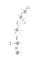
- the raw material 1 is supplied, and electrons are collided with the raw material 1 by the electron impact method to dissociate the bonds of the raw material 1 to generate ionized cluster ions 2.
- the monoatomic ions 4 and the polyatomic ions 6 are formed simultaneously.
- the unstable polyatomic ion 6 may further dissociate.
- mass separation of the generated ions is performed.
- the cluster ions 2 selected by the mass separation are extracted with a predetermined acceleration voltage to form a cluster ion beam.
- the surface of the target T can be processed.
- the raw material 1 may be any of gas, liquid, and solid under a normal temperature and normal pressure environment. Immediately before the electron collides with the raw material 1 in the apparatus, the raw material 1 is gasified.
- cluster ions mean the above-mentioned ionized mass group
- cluster ion beams mean bundles obtained by accelerating and focusing the cluster ions in a vacuum.
- Means a beam that translates into “Cluster size” means the number of atoms or molecules constituting one cluster.
- Patent Document 1 that irradiates a semiconductor wafer with cluster ions, and forms a modified layer in which the constituent elements of the cluster ions are dissolved on the surface of the semiconductor wafer.
- the manufacturing method of the semiconductor epitaxial wafer which has a process and the process of forming an epitaxial layer on the modified layer of the said semiconductor wafer is proposed.
- the technique described in Patent Document 1 since the cluster ions are irradiated onto the surface of the semiconductor wafer, the constituent elements of the cluster ions are locally and highly concentrated compared to the ion implantation region formed by the monomer ion implantation technique. Regions can be formed. Therefore, the technique described in Patent Document 1 can provide a semiconductor epitaxial wafer having a gettering capability that is extremely superior to that of the prior art, and can suppress heavy metal contamination.
- the applicant of the present application also proposes the following method for manufacturing a semiconductor epitaxial wafer in Patent Document 2 in order to provide a method for manufacturing a semiconductor epitaxial wafer having high gettering capability and suppressing the occurrence of epitaxial defects. is doing. That is, in the method for manufacturing a semiconductor epitaxial wafer disclosed in Patent Document 2, the surface of the semiconductor wafer is irradiated with cluster ions, and the surface element of the semiconductor wafer is modified with the constituent elements of the cluster ions in solid solution.
- the cluster ion beam irradiation process disclosed in Patent Documents 1 and 2 depends on the dose amount of the cluster ions to be irradiated, the beam current value, and the wafer diameter of the semiconductor wafer. On the other hand, it took a long time to perform the cluster ion beam irradiation. Therefore, in order to mass-produce semiconductor epitaxial wafers using the semiconductor epitaxial wafer manufacturing method included as a cluster ion beam irradiation step, improvement in throughput is desired.
- Patent Document 2 discloses that in the example, C 3 H 5 clusters are generated from cyclohexane, and the beam current value is 400 ⁇ A.
- the present inventor has recognized that increasing the beam current value is a new problem.
- an object of the present invention is to provide a cluster ion beam generating method capable of increasing the beam current value of a cluster ion beam as compared with the prior art.
- Another object of the present invention is to provide a cluster ion beam irradiation method using this cluster ion beam generation method and a method for manufacturing a semiconductor epitaxial wafer.
- the present inventor has intensively studied to solve the above problems. As a result of diligent study by the present inventor, it was confirmed that the beam current value can be increased to some extent by changing the decomposition conditions of the raw material in the ion source, but the increase was limited. Therefore, the present inventor has focused on the raw material in the ion source, and in particular has focused on the molecular structure of the hydrocarbon-based compound raw material.
- the current value of the cluster ion beam is greatly improved by using branched chain saturated hydrocarbons with a specified structure as the hydrocarbon compound raw material. The present inventor has found out that this can be done, and has completed the present invention. That is, the gist configuration of the present invention is as follows.
- a cluster ion beam generating method comprising hydrogen, wherein the branched chain saturated hydrocarbon is branched only by a tertiary carbon atom.
- the branched chain saturated hydrocarbon has 2 or 3 or more tertiary carbon atoms, and the 2 or 3 or more tertiary carbon atoms are all 1 or 2 or more secondary carbon atoms.
- a cluster ion beam irradiation method comprising irradiating the surface of a semiconductor wafer with a cluster ion beam generated using the cluster ion beam generation method according to any one of (1) to (5).
- the present invention it is possible to provide a cluster ion beam generating method capable of increasing the beam current value of the cluster ion beam as compared with the conventional case. Furthermore, the present invention can provide a cluster ion beam irradiation method capable of increasing the beam current value as compared with the prior art.
- FIG. 1 is a schematic diagram for explaining the basic principle of cluster ion beam generation.
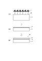
- 2A, 2B, and 2C are schematic cross-sectional views illustrating a method for manufacturing a semiconductor epitaxial wafer 100 using a cluster ion beam irradiation method according to an embodiment of the present invention.
- a cluster ion beam generating method is a cluster ion beam generating method for generating a cluster ion beam having carbon and hydrogen as constituent elements from a hydrocarbon compound material.
- the hydrocarbon-based compound raw material includes a branched chain saturated hydrocarbon having a side chain, and this branched chain saturated hydrocarbon is branched only by a tertiary carbon atom.
- inevitable impurities may be included in the hydrocarbon-based compound raw material.
- the basic principle of the cluster ion beam generation method is as described above with reference to FIG. That is, first, the raw material 1 is supplied, and electrons are collided with the raw material 1 by the electron impact method to dissociate the bonds of the raw material 1 to generate ionized cluster ions 2. Next, mass separation of the generated ions is performed to select the cluster ions 2, and the cluster ions 2 are extracted with a predetermined acceleration voltage to form a cluster ion beam. Thus, a cluster ion beam can be generated. The surface of the arbitrary target T can be irradiated with the cluster ion beam thus obtained.
- CLARIS registered trademark
- Nissin Ion Equipment Co., Ltd. can be used as a cluster ion implantation apparatus using such a principle.
- the above-described hydrocarbon-based compound source gas is used as the source material 1.
- the constituent elements of the cluster ions 2 constituting the obtained cluster ion beam have carbon and hydrogen, and in particular, the constituent elements of the cluster ions 2 can be composed only of carbon and hydrogen.
- the hydrocarbon compound raw material used in the present embodiment will be described in more detail below.
- the hydrocarbon compound raw material is a branched saturated hydrocarbon having a side chain, and it is important that the branched saturated hydrocarbon is branched only by a tertiary carbon atom.
- Such a branched chain saturated hydrocarbon can be represented by the following formula (I).
- R 1 , R 2 and R 3 bonded to the tertiary carbon atom are all independent linear or branched alkyl groups having 1 or 2 or more carbon atoms. is there.
- R 1 , R 2 and R 3 may all be the same alkyl group, any two of them may be the same alkyl group, or all may be different.
- the term “linear” as used herein includes cases where the hydrocarbon has 1 to 3 carbon atoms and cannot be branched. Hereinafter, the term “linear” refers to the same meaning. To tell.
- the branched-chain saturated hydrocarbon used in the present embodiment may be any of gas, liquid and solid under normal pressure and normal pressure environment, and the raw material in a chamber under vacuum (for example, 10 ⁇ 2 Pa or less). It is only necessary that the branched-chain saturated hydrocarbon is gasified immediately before collision with the electrons. That is, when the raw material is introduced into the chamber and collides with electrons, the liquid raw material may be vaporized and supplied into the chamber, or the solid raw material may be heated and vaporized in a vacuum in another apparatus.
- the gas source gas itself may be supplied into the chamber. Examples of the carbon number of such a branched chain saturated hydrocarbon include 4 or more and 16 or less.
- carbon number of a branched chain saturated hydrocarbon shall be 5 or more, and it is more preferable to set it as 6 or more.
- the carbon number of the branched chain saturated hydrocarbon is preferably 10 or less, more preferably 8 or less, and particularly preferably 7 or less. Therefore, the total carbon number of R 1 , R 2 and R 3 can be 3 or more and 15 or less. Further, the total number of carbon atoms of R 1 , R 2 and R 3 is preferably 4 or more, and more preferably 5 or more. On the other hand, the total number of carbon atoms of R 1 , R 2 and R 3 is preferably 9 or less, more preferably 7 or less, and particularly preferably 6 or less.
- the carbon number of R 1 , R 2 and R 3 in the above formula (I) is independently 1 or more and 2 or more as long as the total carbon number described above is satisfied. It can be 3 or more.
- the carbon numbers of R 1 , R 2 and R 3 can be independently 4 or less, 3 or less, and 2 or less. It can be.
- the carbon numbers of R 1 , R 2 and R 3 may all be the same, or any two of them may be the same, or all may be different.
- the present inventor pays attention to this point and uses the branched chain saturated hydrocarbon represented by the above formula (I) as a hydrocarbon-based compound raw material, so that the beam current value of the generated cluster ion beam is compared with the conventional one. The effect was clarified experimentally and the effect was clarified experimentally.
- the beam current value of the cluster ion beam can be greatly increased compared to the conventional case.
- the obtained beam current value can be 1000 ⁇ A or more, 1200 ⁇ A, 1500 ⁇ A or more, and 1800 ⁇ A or more. Furthermore, it can be 2000 ⁇ A or more.
- the branched chain saturated hydrocarbon represented by the above formula (I) preferably has only one tertiary carbon atom. That is, it is preferable that R 1 , R 2 and R 3 in the formula (I) are all linear saturated alkyl groups.
- R 1 can be a methyl group, an ethyl group, an n-propyl group, or an n-butyl group
- R 2 and R 3 can be either a methyl group or an ethyl group.
- branched chain saturated hydrocarbons examples include 2-methylpropane, 2-methylbutane, 2-methylpentane, 2-methylhexane, 2-methylheptane, and the like.
- the branched chain saturated hydrocarbon represented by the above formula (I) has 2 or 3 or more tertiary carbon atoms, and these 2 or 3 or more tertiary carbon atoms are all 1 or 2 or more. It is also preferred to bond via the secondary carbon atom.
- the branched chain saturated hydrocarbon preferably has two tertiary carbon atoms.
- the latter branched chain saturated hydrocarbon can be represented by the following formula (II).
- R 4 bonded to the tertiary carbon atom is a linear saturated alkylene group, and R 5 , R 6 , R 7 and R 8 are all linear.
- a saturated alkyl group is a linear saturated alkylene group.
- the carbon number of the branched chain saturated hydrocarbon represented by the formula (II) is the same as the carbon number of the branched chain saturated hydrocarbon of the formula (I) except that the lower limit is 7. Therefore, the total carbon number of R 4 , R 5 , R 6 , R 7 and R 8 can be 5 or more and 14 or less.
- the total number of carbon atoms of R 4 , R 5 , R 6 , R 7 and R 8 is preferably 5 or more, preferably 6 or more, and more preferably 7 or more.
- the total carbon number of R 4 , R 5 , R 6 , R 7 and R 8 is preferably 9 or less, preferably 8 or less, and preferably 7 or less.
- the carbon number of R 4 , R 5 , R 6 , R 7 and R 8 can be independently 4 or less and 3 or less while satisfying the above-mentioned total carbon number. Can be 2 or less.
- R 4 , R 5 , R 6 , R 7 and R 8 may all have the same number of carbons, or any two, three or four carbons may be the same or all different It may be.
- branched saturated hydrocarbons examples include 2,4-dimethylpentane, 2,4-dimethylhexane, 2,4-dimethylheptane, 2,5-dimethylhexane, 2,5-dimethylheptane, and the like. It can.
- these branched chain saturated hydrocarbons as the hydrocarbon-based compound source gas, the beam current value of the cluster ion beam can be increased more reliably.
- R 4 in formula (II) is preferably a methylene group.
- 2,4-dimethylpentane, 2,4-dimethylhexane, or 2,4-dimethylheptane can be used as the branched chain saturated hydrocarbon according to the above formula (II).
- cluster ions can be generated by a known method as described in the following document.
- Charged particle beam engineering Junzo Ishikawa: ISBN978-4-339-00734-3: Corona
- Electron and ion beam engineering The Institute of Electrical Engineers of Japan: ISBN4-88686-217-9: Ohm
- Cluster ion beam basics and applications ISBN4-526-05765-7: Nikkan Kogyo Shimbun.
- a Nielsen ion source or a Kaufman ion source is used to generate positively charged cluster ions
- a large current negative ion source using a volume generation method is used to generate negatively charged cluster ions. It is done.
- the acceleration voltage per carbon atom of the generated cluster ions is more than 0 keV / atom and 50 keV / atom or less, preferably 40 keV / atom or less.
- the cluster size can be 2 to 50 or less, although it depends on the branched chain saturated hydrocarbon constituting the hydrocarbon compound raw material.
- two methods of (1) electrostatic acceleration and (2) high frequency acceleration are generally used for adjusting the acceleration voltage.
- As the former method there is a method in which a plurality of electrodes are arranged at equal intervals and an equal voltage is applied between them to create an equal acceleration electric field in the axial direction.
- As the latter method there is a linear linac method in which ions are accelerated using a high frequency while running linearly.
- the cluster size and beam current value of the cluster ion beam can be adjusted by adjusting the pressure of the vacuum vessel (the flow rate of the introduced gas) and the voltage applied to the filament during ionization.
- the cluster size can be determined by using a mass separation method using a quadrupole high-frequency electric field or a single-focusing sector magnetic field.
- FIGS. 2A, 2B, and 2C a cluster ion beam irradiation method according to another embodiment of the present invention will be described with reference to FIGS. 2A, 2B, and 2C (hereinafter, FIGS. 2A to 2C).
- the same components are denoted by the same reference numerals, and description thereof is omitted.
- 2A to 2C for convenience of explanation, the thickness of the epitaxial layer 20 is exaggerated with respect to the semiconductor wafer 10 unlike the actual thickness ratio.
- Cluster ion beam irradiation method As shown in FIG. 2A, in the cluster ion beam irradiation method according to the embodiment of the present invention, the surface 10A of the semiconductor wafer 10 is irradiated with the cluster ion beam C generated by using the embodiment of the cluster ion beam generation method. .
- the semiconductor wafer 10 includes, for example, a bulk single crystal wafer made of silicon or a compound semiconductor (GaAs, GaN, SiC) and having no epitaxial layer on the surface.
- a silicon wafer obtained by slicing a single crystal silicon ingot grown by the Czochralski method (CZ method) or the floating zone melting method (FZ method) with a wire saw or the like can be used. Further, carbon and / or nitrogen may be added to the silicon wafer. Further, an arbitrary impurity dopant may be added to be n-type or p-type.
- an epitaxial semiconductor wafer in which a semiconductor epitaxial layer is formed on the surface of a bulk semiconductor wafer can also be used.
- the dose amount of cluster ions can be adjusted by controlling the beam current value and the ion irradiation time.
- the carbon dose of the cluster ions can be set to 1 ⁇ 10 13 to 1 ⁇ 10 16 atoms / cm 2 , for example.
- the beam current value can be 1000 ⁇ A or more, 1200 ⁇ A or more, 1500 ⁇ A or more, 1800 ⁇ A or more, and further 2000 ⁇ A or more. be able to.
- the surface 10A of the semiconductor wafer 10 is irradiated with the cluster ion beam C generated by using the embodiment of the cluster ion beam generating method described above (FIG. 2A).
- a modified layer 18 in which constituent elements of cluster ions are dissolved is formed in the part (FIG. 2B), and an epitaxial layer 20 is formed on the modified layer 18 of the semiconductor wafer 10 (FIG. 2C).
- the semiconductor epitaxial wafer 100 can be manufactured by including an epitaxial layer forming step.
- the modified layer 18 formed by the cluster ion beam irradiation process is a region in which carbon is solid-dissolved locally at the interstitial position or the substitution position of the crystal in the surface portion of the semiconductor wafer 10 and has strong gettering. Can work as a site.
- the epitaxial layer 20 formed on the modified layer 18 includes a silicon epitaxial layer, and can be formed under general conditions.
- a source gas such as dichlorosilane or trichlorosilane is introduced into the chamber using hydrogen as a carrier gas, and the growth temperature varies depending on the source gas used, but the semiconductor is formed by a CVD method at a temperature in the range of about 1000 to 1200 ° C. It can be epitaxially grown on the wafer 10.
- the thickness of the epitaxial layer 20 is preferably in the range of 1 to 15 ⁇ m.
- Example 2 Invention Example 2, in Example 1, except that 2,4-dimethylpentane (C 7 H 16 ) was used as a raw material instead of 2-methylpentane, cluster ionized C 3 H 5 clusters were obtained in the same manner as in Example 1. Ions were generated. The beam current value of the obtained cluster ion beam was 1800 ⁇ A.
- Example 1 Inventional example 1, except that cyclohexane (C 6 H 12 ) was used as a raw material instead of 2-methylpentane, cluster ionized C 3 H 5 cluster ions were produced in the same manner as Example 1. The beam current value of the obtained cluster ion beam was 800 ⁇ A.
- Example 1 (Comparative Example 1) In Example 1, except that hexane (C 6 H 14 ) was used as a raw material instead of 2-methylpentane, cluster ionized C 3 H 5 cluster ions were produced in the same manner as Example 1. The beam current value of the obtained cluster ion beam was 800 ⁇ A.
- Example 2 (Comparative Example 2) In Example 1, except that 2,3-dimethylbutane (C 6 H 14 ) was used as a raw material instead of 2-methylpentane, cluster ionized C 3 H 5 clusters were obtained in the same manner as in Example 1. Ions were generated. The beam current value of the obtained cluster ion beam was 20 ⁇ A.
- the present invention it is possible to provide a cluster ion beam generating method capable of increasing the beam current value of the cluster ion beam as compared with the conventional case. Furthermore, the present invention can provide a cluster ion beam irradiation method capable of increasing the beam current value as compared with the prior art. Therefore, it is particularly useful in the semiconductor industry.
Landscapes
- Chemical & Material Sciences (AREA)
- Chemical Kinetics & Catalysis (AREA)
- Engineering & Computer Science (AREA)
- Materials Engineering (AREA)
- Mechanical Engineering (AREA)
- Metallurgy (AREA)
- Organic Chemistry (AREA)
- Physical Vapour Deposition (AREA)
- Recrystallisation Techniques (AREA)
Abstract
Description
本発明の一実施形態によるクラスターイオンビーム生成方法は、炭化水素系化合物原料から、構成元素に炭素および水素を有するクラスターイオンのビームを生成するクラスターイオンビーム生成方法である。ここで、炭化水素系化合物原料は、側鎖を備える分岐鎖飽和炭化水素を含み、この分岐鎖飽和炭化水素は第3級炭素原子によってのみ分岐する。なお、炭化水素系化合物原料中に不可避の不純物は含まれ得る。

ここで、上記式(I)において、第3級炭素原子に結合するR1、R2およびR3は、いずれも、炭素数を1または2以上とする独立した直鎖状または分岐アルキル基である。R1、R2およびR3は全て同じアルキル基であってもよいし、いずれか2つが同じアルキル基であってもよいし、全て異なっていてもよい。なお、ここで言う「直鎖状」とは、炭素数が1以上3以下の、分岐が生じ得ない炭化水素である場合も含むものであり、以下、同様の意味で「直鎖状」と言う。
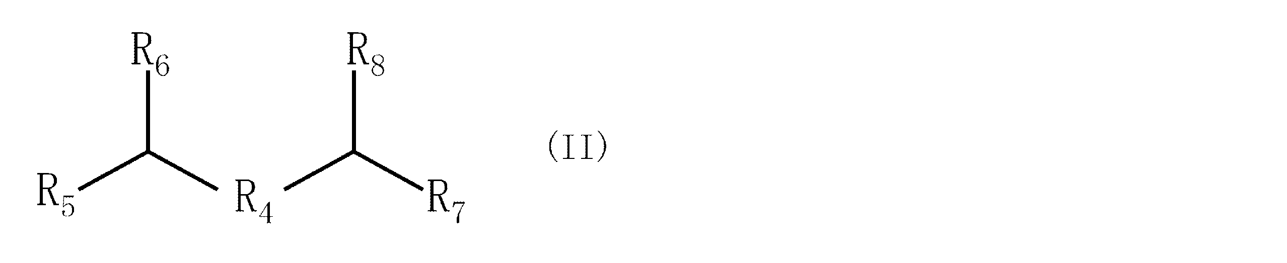
ここで、上記式(II)において、第3級炭素原子に結合するR4は直鎖状の飽和アルキレン基であり、R5、R6、R7およびR8は、いずれも直鎖状の飽和アルキル基である。
図2Aに示すように、本発明の一実施形態によるクラスターイオンビーム照射方法は、上記クラスターイオンビーム生成方法の実施形態を用いて生成したクラスターイオンビームCを、半導体ウェーハ10の表面10Aに照射する。本実施形態では、ビーム電流値が従来よりも増大したクラスターイオンビーム照射を行うことができる。そのため、従来技術と同じドーズ量のクラスターイオンを照射するのであれば、従来技術に比べて照射時間を短くすることができる。
図2A-図2Cに示すように、上記クラスターイオンビーム生成方法の実施形態を用いて生成したクラスターイオンビームCを半導体ウェーハ10の表面10Aに照射して(図2A)、該半導体ウェーハ10の表面部に、クラスターイオンの構成元素が固溶した改質層18を形成する(図2B)クラスターイオンビーム照射工程と、半導体ウェーハ10の改質層18上にエピタキシャル層20を形成する(図2C)エピタキシャル層形成工程と、を含むことで、半導体エピタキシャルウェーハ100を製造することができる。
クラスターイオン発生装置(日新イオン機器社製、型番:CLARIS)を用いて、2-メチルペンタン(C6H14)を原料として用い、クラスターイオン化したC3H5のクラスターイオンを生成した。得られたクラスターイオンビームのビーム電流値は2000μAであった。
発明例1において、2-メチルペンタンに替えて、2,4-ジメチルペンタン(C7H16)を原料に用いた以外は、発明例1と同様にして、クラスターイオン化したC3H5のクラスターイオンを生成した。得られたクラスターイオンビームのビーム電流値は1800μAであった。
発明例1において、2-メチルペンタンに替えて、シクロヘキサン(C6H12)を原料に用いた以外は、発明例1と同様にして、クラスターイオン化したC3H5のクラスターイオンを生成した。得られたクラスターイオンビームのビーム電流値は800μAであった。
発明例1において、2-メチルペンタンに替えて、ヘキサン(C6H14)を原料に用いた以外は、発明例1と同様にして、クラスターイオン化したC3H5のクラスターイオンを生成した。得られたクラスターイオンビームのビーム電流値は800μAであった。
発明例1において、2-メチルペンタンに替えて、2,3-ジメチルブタン(C6H14)を原料に用いた以外は、発明例1と同様にして、クラスターイオン化したC3H5のクラスターイオンを生成した。得られたクラスターイオンビームのビーム電流値は20μAであった。

発明例1,2では、従来例1により得られるビーム電流値の、倍以上のビーム電流値が得られることが確認できた。発明例1,2は、従来例1および比較例1と異なり、第3級炭素原子を含むために結合乖離が生じやすくなり、その結果、C3H5のクラスターイオンを取り出しやすくなったためだと考えられる。一方、比較例2には、第3級炭素原子が含まれるものの、放電が多く、クラスターイオンビームの形成が困難であったため、ビーム電流値は従来例1よりも小さかった。これは2,3-ジメチルブタン中央の第三級炭素間の結合が非常に弱くなっているため、クラスターイオンを生成する際の制御が困難なほど、イオン生成が爆発的に進んだためだと考えられる。
2 クラスターイオン
4 単原子イオン
6 多原子イオン
10 半導体ウェーハ
10A 半導体ウェーハの表面
18 改質層
20 エピタキシャル層
100 半導体エピタキシャルウェーハ
C クラスターイオンビーム
T ターゲット
Claims (6)
- 炭化水素系化合物原料から、構成元素に炭素および水素を有するクラスターイオンのビームを生成するクラスターイオンビーム生成方法であって、
前記炭化水素系化合物原料は、側鎖を備える分岐鎖飽和炭化水素を含み、前記分岐鎖飽和炭化水素は第3級炭素原子によってのみ分岐することを特徴とするクラスターイオンビーム生成方法。 - 前記分岐鎖飽和炭化水素は前記第3級炭素原子を1つのみ有する、請求項1に記載のクラスターイオンビーム生成方法。
- 前記分岐鎖飽和炭化水素は前記第3級炭素原子を2または3以上有し、前記2または3以上の前記第3級炭素原子は、いずれも1または2以上の第2級炭素原子を介して結合する、請求項1に記載のクラスターイオンビーム生成方法。
- 前記分岐鎖飽和炭化水素は前記第3級炭素原子を2つ有する、請求項3に記載のクラスターイオンビーム生成方法。
- 前記2つの前記第3級炭素原子が、1つの第2級炭素原子を介して結合する、請求項4に記載のクラスターイオンビーム生成方法。
- 請求項1~5のいずれか1項に記載のクラスターイオンビーム生成方法を用いて生成したクラスターイオンビームを、半導体ウェーハの表面に照射することを特徴とするクラスターイオンビーム照射方法。
Priority Applications (2)
| Application Number | Priority Date | Filing Date | Title |
|---|---|---|---|
| CN201780023782.2A CN109154072A (zh) | 2016-07-05 | 2017-06-29 | 簇离子束生成方法和使用该方法的簇离子束照射方法 |
| KR1020187025839A KR102165217B1 (ko) | 2016-07-05 | 2017-06-29 | 클러스터 이온 빔 생성 방법 및 그것을 이용한 클러스터 이온 빔 조사 방법 |
Applications Claiming Priority (2)
| Application Number | Priority Date | Filing Date | Title |
|---|---|---|---|
| JP2016-133588 | 2016-07-05 | ||
| JP2016133588A JP6750351B2 (ja) | 2016-07-05 | 2016-07-05 | クラスターイオンビーム生成方法およびそれを用いたクラスターイオンビーム照射方法 |
Publications (1)
| Publication Number | Publication Date |
|---|---|
| WO2018008533A1 true WO2018008533A1 (ja) | 2018-01-11 |
Family
ID=60912850
Family Applications (1)
| Application Number | Title | Priority Date | Filing Date |
|---|---|---|---|
| PCT/JP2017/024029 Ceased WO2018008533A1 (ja) | 2016-07-05 | 2017-06-29 | クラスターイオンビーム生成方法およびそれを用いたクラスターイオンビーム照射方法 |
Country Status (5)
| Country | Link |
|---|---|
| JP (1) | JP6750351B2 (ja) |
| KR (1) | KR102165217B1 (ja) |
| CN (1) | CN109154072A (ja) |
| TW (1) | TWI638058B (ja) |
| WO (1) | WO2018008533A1 (ja) |
Cited By (2)
| Publication number | Priority date | Publication date | Assignee | Title |
|---|---|---|---|---|
| JP2024094041A (ja) * | 2022-12-27 | 2024-07-09 | 株式会社Sumco | クラスターイオンビームの生成方法及びクラスターイオンの注入方法 |
| JP2024094045A (ja) * | 2022-12-27 | 2024-07-09 | 株式会社Sumco | クラスターイオンビームの生成方法及びクラスターイオンの注入方法 |
Families Citing this family (1)
| Publication number | Priority date | Publication date | Assignee | Title |
|---|---|---|---|---|
| JP6801682B2 (ja) * | 2018-02-27 | 2020-12-16 | 株式会社Sumco | 半導体エピタキシャルウェーハの製造方法及び半導体デバイスの製造方法 |
Citations (2)
| Publication number | Priority date | Publication date | Assignee | Title |
|---|---|---|---|---|
| JP2014183041A (ja) * | 2013-03-15 | 2014-09-29 | Nissin Ion Equipment Co Ltd | イオン源および磁界発生方法 |
| JP2016051729A (ja) * | 2014-08-28 | 2016-04-11 | 株式会社Sumco | 半導体エピタキシャルウェーハおよびその製造方法、ならびに、固体撮像素子の製造方法 |
Family Cites Families (6)
| Publication number | Priority date | Publication date | Assignee | Title |
|---|---|---|---|---|
| EP1245036B1 (en) * | 1999-12-13 | 2013-06-19 | Semequip, Inc. | Ion implantation ion source |
| KR101455404B1 (ko) * | 2005-12-09 | 2014-10-27 | 세미이큅, 인코포레이티드 | 탄소 클러스터의 주입에 의한 반도체 디바이스의 제조를위한 시스템 및 방법 |
| US8981322B2 (en) * | 2009-02-04 | 2015-03-17 | Tel Epion Inc. | Multiple nozzle gas cluster ion beam system |
| US8455060B2 (en) * | 2009-02-19 | 2013-06-04 | Tel Epion Inc. | Method for depositing hydrogenated diamond-like carbon films using a gas cluster ion beam |
| JP2012157162A (ja) | 2011-01-26 | 2012-08-16 | Sumitomo Electric Ind Ltd | 電力伝達用絶縁回路および電力変換装置 |
| WO2014165165A1 (en) | 2013-03-13 | 2014-10-09 | Centrotherm Photovoltaics Usa, Inc. | Temperature management in chlorination processes and systems related thereto |
-
2016
- 2016-07-05 JP JP2016133588A patent/JP6750351B2/ja active Active
-
2017
- 2017-06-29 WO PCT/JP2017/024029 patent/WO2018008533A1/ja not_active Ceased
- 2017-06-29 CN CN201780023782.2A patent/CN109154072A/zh active Pending
- 2017-06-29 KR KR1020187025839A patent/KR102165217B1/ko active Active
- 2017-07-04 TW TW106122314A patent/TWI638058B/zh active
Patent Citations (2)
| Publication number | Priority date | Publication date | Assignee | Title |
|---|---|---|---|---|
| JP2014183041A (ja) * | 2013-03-15 | 2014-09-29 | Nissin Ion Equipment Co Ltd | イオン源および磁界発生方法 |
| JP2016051729A (ja) * | 2014-08-28 | 2016-04-11 | 株式会社Sumco | 半導体エピタキシャルウェーハおよびその製造方法、ならびに、固体撮像素子の製造方法 |
Cited By (4)
| Publication number | Priority date | Publication date | Assignee | Title |
|---|---|---|---|---|
| JP2024094041A (ja) * | 2022-12-27 | 2024-07-09 | 株式会社Sumco | クラスターイオンビームの生成方法及びクラスターイオンの注入方法 |
| JP2024094045A (ja) * | 2022-12-27 | 2024-07-09 | 株式会社Sumco | クラスターイオンビームの生成方法及びクラスターイオンの注入方法 |
| JP7768120B2 (ja) | 2022-12-27 | 2025-11-12 | 株式会社Sumco | クラスターイオンビームの生成方法及びクラスターイオンの注入方法 |
| JP7768119B2 (ja) | 2022-12-27 | 2025-11-12 | 株式会社Sumco | クラスターイオンビームの生成方法及びクラスターイオンの注入方法 |
Also Published As
| Publication number | Publication date |
|---|---|
| JP2018003119A (ja) | 2018-01-11 |
| TWI638058B (zh) | 2018-10-11 |
| TW201812057A (zh) | 2018-04-01 |
| KR102165217B1 (ko) | 2020-10-13 |
| CN109154072A (zh) | 2019-01-04 |
| KR20180111950A (ko) | 2018-10-11 |
| JP6750351B2 (ja) | 2020-09-02 |
Similar Documents
| Publication | Publication Date | Title |
|---|---|---|
| CN104781919B (zh) | 半导体外延晶片的制造方法、半导体外延晶片以及固体摄像元件的制造方法 | |
| TW200816255A (en) | Ion beam apparatus for ion implantation | |
| JP6237127B2 (ja) | イオン源、その運転方法および電子銃 | |
| JP6237133B2 (ja) | イオン源および磁界発生方法 | |
| JP4416632B2 (ja) | ガスクラスターイオンビーム照射装置およびガスクラスターのイオン化方法 | |
| CN106663582B (zh) | 串列式加速器及离子植入系统 | |
| JP6750351B2 (ja) | クラスターイオンビーム生成方法およびそれを用いたクラスターイオンビーム照射方法 | |
| TWI443717B (zh) | 增加含碳離子化種類的產量的方法、增加含碳離子化種類電流的方法以及將含碳離子化種類植入至基底中的方法 | |
| JP6229258B2 (ja) | 貼り合わせウェーハの製造方法および貼り合わせウェーハ | |
| TWI866976B (zh) | 離子植入系統以及用於操作高能離子植入機之方法 | |
| JPH10162770A (ja) | ドーピング装置およびドーピング処理方法 | |
| JP6265291B2 (ja) | 貼り合わせウェーハの製造方法および貼り合わせウェーハ | |
| JP7040478B2 (ja) | クラスターイオンビーム生成方法及びクラスターイオンビーム照射方法 | |
| JP2003327423A (ja) | 異種元素が導入されたチューブ状物質の製造方法 | |
| CN114600222B (zh) | 用于离子植入的等离子体浸渍方法 | |
| TW201714197A (zh) | 加速器/減速器、離子植入系統及控制加速器/減速器中的離子束的方法 | |
| JP7768119B2 (ja) | クラスターイオンビームの生成方法及びクラスターイオンの注入方法 | |
| US20150179451A1 (en) | Method for processing graphene, method for producing graphene nanoribbons, and graphene nanoribbons | |
| JP2007073534A (ja) | ドーピング処理装置 | |
| Tang et al. | Beam current improvement and source life performance of diboron tetrafluoride (B 2 F 4) for boron implantation on applied materials VIISta high current implanters | |
| JP2000235959A (ja) | ドーピング処理方法 | |
| JP2005045114A (ja) | ダイヤモンドへの異種元素導入方法並びにダイヤモンド及びダイヤモンドを用いたトランジスタ素子、電子放出素子若しくは発光素子 | |
| JPH11288682A (ja) | ド―ピング装置およびド―ピング処理方法 | |
| WO2013019432A2 (en) | Method for uninterrupted production of a polyatomic boron molecular ion beam with self-cleaning |
Legal Events
| Date | Code | Title | Description |
|---|---|---|---|
| ENP | Entry into the national phase |
Ref document number: 20187025839 Country of ref document: KR Kind code of ref document: A |
|
| WWE | Wipo information: entry into national phase |
Ref document number: 1020187025839 Country of ref document: KR |
|
| 121 | Ep: the epo has been informed by wipo that ep was designated in this application |
Ref document number: 17824138 Country of ref document: EP Kind code of ref document: A1 |
|
| NENP | Non-entry into the national phase |
Ref country code: DE |
|
| 122 | Ep: pct application non-entry in european phase |
Ref document number: 17824138 Country of ref document: EP Kind code of ref document: A1 |