WO2018003519A1 - 実装装置および実装方法 - Google Patents
実装装置および実装方法 Download PDFInfo
- Publication number
- WO2018003519A1 WO2018003519A1 PCT/JP2017/022117 JP2017022117W WO2018003519A1 WO 2018003519 A1 WO2018003519 A1 WO 2018003519A1 JP 2017022117 W JP2017022117 W JP 2017022117W WO 2018003519 A1 WO2018003519 A1 WO 2018003519A1
- Authority
- WO
- WIPO (PCT)
- Prior art keywords
- substrate
- holding
- semiconductor chip
- holding unit
- backup stage
- Prior art date
- Legal status (The legal status is an assumption and is not a legal conclusion. Google has not performed a legal analysis and makes no representation as to the accuracy of the status listed.)
- Ceased
Links
Images





Classifications
-
- H—ELECTRICITY
- H10—SEMICONDUCTOR DEVICES; ELECTRIC SOLID-STATE DEVICES NOT OTHERWISE PROVIDED FOR
- H10P—GENERIC PROCESSES OR APPARATUS FOR THE MANUFACTURE OR TREATMENT OF DEVICES COVERED BY CLASS H10
- H10P72/00—Handling or holding of wafers, substrates or devices during manufacture or treatment thereof
- H10P72/04—Apparatus for manufacture or treatment
- H10P72/0428—Apparatus for mechanical treatment or grinding or cutting
-
- H—ELECTRICITY
- H10—SEMICONDUCTOR DEVICES; ELECTRIC SOLID-STATE DEVICES NOT OTHERWISE PROVIDED FOR
- H10P—GENERIC PROCESSES OR APPARATUS FOR THE MANUFACTURE OR TREATMENT OF DEVICES COVERED BY CLASS H10
- H10P72/00—Handling or holding of wafers, substrates or devices during manufacture or treatment thereof
- H10P72/04—Apparatus for manufacture or treatment
- H10P72/0438—Apparatus for making assemblies not otherwise provided for, e.g. package constructions
-
- H—ELECTRICITY
- H10—SEMICONDUCTOR DEVICES; ELECTRIC SOLID-STATE DEVICES NOT OTHERWISE PROVIDED FOR
- H10P—GENERIC PROCESSES OR APPARATUS FOR THE MANUFACTURE OR TREATMENT OF DEVICES COVERED BY CLASS H10
- H10P72/00—Handling or holding of wafers, substrates or devices during manufacture or treatment thereof
- H10P72/06—Apparatus for monitoring, sorting, marking, testing or measuring
- H10P72/0606—Position monitoring, e.g. misposition detection or presence detection
-
- H—ELECTRICITY
- H10—SEMICONDUCTOR DEVICES; ELECTRIC SOLID-STATE DEVICES NOT OTHERWISE PROVIDED FOR
- H10P—GENERIC PROCESSES OR APPARATUS FOR THE MANUFACTURE OR TREATMENT OF DEVICES COVERED BY CLASS H10
- H10P72/00—Handling or holding of wafers, substrates or devices during manufacture or treatment thereof
- H10P72/70—Handling or holding of wafers, substrates or devices during manufacture or treatment thereof for supporting or gripping
-
- H—ELECTRICITY
- H10—SEMICONDUCTOR DEVICES; ELECTRIC SOLID-STATE DEVICES NOT OTHERWISE PROVIDED FOR
- H10W—GENERIC PACKAGES, INTERCONNECTIONS, CONNECTORS OR OTHER CONSTRUCTIONAL DETAILS OF DEVICES COVERED BY CLASS H10
- H10W72/00—Interconnections or connectors in packages
- H10W72/071—Connecting or disconnecting
-
- H—ELECTRICITY
- H10—SEMICONDUCTOR DEVICES; ELECTRIC SOLID-STATE DEVICES NOT OTHERWISE PROVIDED FOR
- H10W—GENERIC PACKAGES, INTERCONNECTIONS, CONNECTORS OR OTHER CONSTRUCTIONAL DETAILS OF DEVICES COVERED BY CLASS H10
- H10W72/00—Interconnections or connectors in packages
- H10W72/071—Connecting or disconnecting
- H10W72/072—Connecting or disconnecting of bump connectors
-
- H—ELECTRICITY
- H10—SEMICONDUCTOR DEVICES; ELECTRIC SOLID-STATE DEVICES NOT OTHERWISE PROVIDED FOR
- H10W—GENERIC PACKAGES, INTERCONNECTIONS, CONNECTORS OR OTHER CONSTRUCTIONAL DETAILS OF DEVICES COVERED BY CLASS H10
- H10W74/00—Encapsulations, e.g. protective coatings
- H10W74/10—Encapsulations, e.g. protective coatings characterised by their shape or disposition
- H10W74/15—Encapsulations, e.g. protective coatings characterised by their shape or disposition on active surfaces of flip-chip devices, e.g. underfills
Definitions
- the present invention relates to a mounting apparatus and a mounting method. Specifically, the present invention relates to a mounting apparatus and a mounting method for mounting a plurality of semiconductor chips on a substrate by thermocompression bonding.
- COW method chip-on-wafer method
- the COW method is a method in which a semiconductor chip is bonded and mounted on a wafer on which electronic components to be divided into semiconductor chips are fabricated.
- FIG. 10 the upper surface of the wafer is shown in FIG. FIG. 10B is a cross-sectional view taken along the line AA, in which a large number of semiconductor chips C are mounted using a single wafer as a substrate W.
- the semiconductor chip C on W is thermocompression bonded by the bonding head 7.
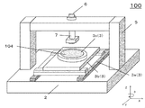
- the mounting apparatus 100 of FIG. 13 when a substrate W having a relatively large area, such as a wafer, is targeted, the substrate W is in a plane (in the ⁇ direction with the X, Y, and Z directions as rotation axes). It is necessary to increase the size of the XY ⁇ table 103 to be moved.
- the rigidity of the suction stage 104 may be different depending on the in-plane position of the substrate W, or the stage surface may be slightly inclined, and the semiconductor chip C is formed when thermobonding is performed by the bonding head 7. Misalignment may occur.
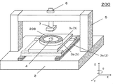
- Patent Document 2 a mounting apparatus 200 as shown in FIG. 14 has appeared (Patent Document 2).
- the backup stage 4 that supports the region pressed by the pressing surface of the bonding head 7 from the back surface of the substrate W is disposed immediately below the bonding head 7, and the substrate W is a substrate disposed on the XY ⁇ movable mechanism 3.
- the position is adjusted by the gripping means 208.
- the X-direction movable portion 3b, the Y-direction movable portion 3a, and the ⁇ -direction movable portion 3C of the XY ⁇ movable mechanism 3 have a hollow structure, and the backup stage 4 can be fixed to the base 2. it can.
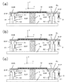
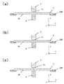
- FIG. 15A shows a state where the backup stage 4 supports the same area as the pressing surface of the bonding head 7 formed by the attachment tool 71 from the back surface of the substrate W, and shows a state before thermocompression bonding by the bonding head 7. Yes.
- FIG. 15B the bonding head 7 is lowered, and the semiconductor chip C in the pressing region is thermocompression bonded.
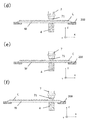
- the bonding head 7 is raised, and the substrate gripping means 208 raises the substrate W to separate the back surface of the substrate W from the backup stage 4 (FIG. 15C). Since the back surface of the substrate W has moved away from the backup stage 4, the substrate W gripped by the substrate gripping means 208 can be moved in the horizontal direction by driving the XY ⁇ movable mechanism 3, so that the semiconductor chip C to be thermocompression bonded next time Is aligned between the bonding head 7 and the backup stage 4 (FIG. 16D). Then, the substrate gripping means 208 is lowered to a position where the back surface of the substrate W is in close contact with the backup stage 4, and is in a preparation stage for performing thermocompression bonding similar to FIG. 15A (FIG. 16E).
- JP2015-170646A Japanese Patent Application No. 2016-067990
- the substrate gripping means 208 grips the periphery of the substrate W.
- the backup stage 4 The substrate gripping means 208 interferes with the thermocompression bonding. For example, even if an attempt is made to move the substrate W to the right side (for two semiconductor chips having a moving pitch) after thermocompression bonding in the state of FIG. 16 (f), the substrate holding means 208 interferes with the backup stage 4. For this reason, the semiconductor chip C at the position where the backup stage 4 and the substrate gripping means 208 interfere cannot be thermocompression bonded.
- the present invention has been made in view of the above problems, and when a semiconductor chip temporarily fixed to a substrate such as a silicon wafer is subjected to thermocompression bonding, uniform conditions are obtained until the semiconductor chip is temporarily fixed near the outer periphery of the substrate.
- a mounting apparatus and a mounting method capable of performing thermocompression bonding with the above are provided.
- a mounting device for thermocompression bonding a semiconductor chip to a substrate A bonding head having a pressing surface for pressing a semiconductor chip against the substrate, a backup stage for supporting a region pressed by the pressing surface from the back surface of the substrate, and a peripheral portion of the substrate using a holding portion Board holding means for holding
- the mounting apparatus has a function of changing a position of the holding unit that holds the board by the board holding means.
- the mounting apparatus has a function of changing the position where the substrate gripping means grips the substrate by moving the position of the holding portion along the periphery.
- Invention of Claim 3 is the mounting apparatus of Claim 1, Comprising: A mounting apparatus in which the substrate holding means has a function of having a plurality of the holding portions, causing only a part of the plurality of holding portions to hold the peripheral portion of the substrate, and retreating the other holding portions from the peripheral portion of the substrate. It is.
- the invention according to claim 4 A mounting method for thermocompression bonding a semiconductor chip temporarily fixed to a substrate, Using a bonding head that thermocompression-bonds the semiconductor chip, and a backup stage that supports the substrate from the back as a pair with the bonding head, In the process of sequentially thermocompression bonding semiconductor chips on the substrate while moving the substrate by a substrate gripping means that partially grips the peripheral edge of the substrate, In this mounting method, the position where the substrate gripping means grips the substrate is changed at least once.
- the present invention has been made in view of the above problems, and when a semiconductor chip temporarily fixed to a substrate such as a silicon wafer is subjected to thermocompression bonding, uniform conditions are obtained until the semiconductor chip is temporarily fixed near the outer periphery of the substrate. Thermocompression bonding can be performed.
- FIG. It is a figure of the state of the board
- FIG. 1 It is a figure which shows a mode that the position of the holding part holding a board
- thermocompression bonding area region from the board
- the mounting apparatus 1 which is one embodiment according to the present invention shown in FIG. 1 will be described.
- the left-right direction in the drawing is described as the X-axis direction
- the depth direction orthogonal thereto is the Y-axis direction
- the up-down direction is the Z-axis direction
- the direction of rotation about the Z-axis is the ⁇ direction.
- the mounting apparatus 1 is for thermocompression bonding of a semiconductor chip C temporarily fixed to a substrate W as shown in FIG.
- a silicon wafer is assumed as the substrate W, but the object of the present invention is not limited to this, and a substrate made of a non-silicon-based semiconductor, ceramics, glass epoxy, or the like may be used. .
- the mounting apparatus 1 is capable of thermocompression bonding a plurality of semiconductor chips C temporarily fixed on the substrate W at the same time as illustrated in FIG. 3, a backup stage 4, a frame 5, a pressure bonding unit 6, a bonding head 7 and a substrate gripping means 8.
- the base 2 is a main structure constituting the mounting apparatus 1, and supports the XY ⁇ movable mechanism 3, the backup stage 4, and the frame 5.
- the XY ⁇ movable mechanism 3 moves the substrate W gripped by the substrate gripping means 8 to an arbitrary position (in the direction of the substrate W surface).
- the Y direction movable part 3a which can move to the base 2 with respect to the base 2 is provided
- the X direction movable part 3b is provided on the Y direction movable part 3a
- the X direction movable part 3b is provided.
- the present invention is not limited to this, and any configuration that can adjust the position in the X, Y, and ⁇ directions may be used.
- it is necessary that the XY ⁇ movable mechanism 3 does not contact the backup stage 4 within the movable range of the XY ⁇ movable mechanism 3.
- the backup stage 4 supports the substrate W from the back surface to which the semiconductor chip C is not temporarily fixed when the semiconductor chip C on the substrate W is thermocompression bonded by the bonding head 7. It is desirable to have a function of adsorbing and holding.
- the backup stage 4 may include a heater. This heater performs heating from the substrate W side during thermocompression bonding by the bonding head 7. *
- the upper surface of the backup stage 4 needs to have a shape that supports a region pressed by the bonding head 7, but if it is too wide, it is not preferable because interference with other components tends to occur.
- the pressing surface of the bonding head 7 and the upper surface of the backup stage 4 form a pair, so that pressurization can be performed with the same parallelism regardless of the position of the substrate W. .
- the backup stage 4 since only the backup stage 4 holds the substrate W when performing thermocompression bonding, heat conduction from the heating surface of the substrate W to the periphery of the substrate W in a state heated by the bonding head 7 and the backup stage 4. Is constant, and stable thermocompression bonding is possible at any position within the substrate W surface.
- the frame 5 supports the crimping unit 6.
- the support frame 5 has a portal shape. This is because it is also suitable when the pressure applied by the crimping unit 6 is large.
- the crimping unit 6 moves the bonding head 7 in the Z-axis direction.
- the crimping unit 6 includes a servo motor and a ball screw (not shown).
- the crimping unit 6 is configured to generate a driving force in the axial direction of the ball screw by rotating the ball screw by a servo motor.
- the crimping unit 6 is attached to the support frame 5 so that the axial direction of the ball screw is in the Z-axis direction perpendicular to the upper surface of the backup stage 4. That is, the crimping unit 6 is configured to generate a driving force (pressing force) in the Z-axis direction.
- the crimping unit 6 is configured to be able to arbitrarily set the pressing force in the Z-axis direction by controlling the output of the servo motor.
- the crimping unit 6 is composed of a servo motor and a ball screw, but is not limited to this, and may be composed of a pneumatic actuator, a hydraulic actuator, or a voice coil motor.
- the bonding head 7 transmits the driving force of the crimping unit 6 to the semiconductor chip C, and pressurizes the semiconductor chip C to perform thermocompression bonding.
- the bonding head 7 includes a heater for heating the semiconductor chip C.
- an attachment tool 71 as shown in FIG. 15 is provided at the tip of the bonding head 7, and the pressing surface 71 ⁇ / b> S formed by the attachment tool 71 has a shape for simultaneously pressing a plurality of semiconductor chips C. ing.
- the bonding head 7 is attached to a ball screw nut (not shown) constituting the crimping unit 6. That is, the bonding head 7 is disposed so as to face the backup stage 4 in parallel. That is, the bonding head 7 is moved in the Z-axis direction by the pressure-bonding unit 6 and thereby approaches the backup stage 4.
- the substrate gripping means 8 is provided in the XY ⁇ movable mechanism 3 and partially grips the peripheral edge of the substrate W by the holding portion 80.
- the substrate W gripped by the substrate gripping means 8 can be moved to an arbitrary position by the XY ⁇ movable mechanism 3 and rotated about the Z axis. With such an operation, the substrate W is arranged in the region pressed by the bonding head 7 and the backup stage 4 so that the XY position and the ⁇ direction of the semiconductor chip C to be thermocompressed are aligned.
- an image recognition means such as a two-field camera when aligning the semiconductor chip C to be thermocompression bonded with the bonding head 7.
- the holding unit 80 constituting the substrate gripping means 8 partially grips the peripheral edge of the substrate W, and there may be one holding unit 80, but a plurality of holding units 80 are provided for stable gripping. desirable.
- the holding unit 80 is desirably provided with an adsorption function in order to reliably hold the substrate W, but may be configured to increase the holding force with a micro suction cup or an adhesive substance.
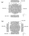
- FIGS. 2 (a) and 2 (b) Examples are shown in FIGS. 2 (a) and 2 (b).
- 2A shows a state in which the substrate W is held by the holding unit 80X1 and the holding unit 80X2 that face each other in the X direction
- FIG. 2B shows a state in which the substrate W is held by the holding unit 80Y1 and the holding unit 80Y2 that face each other in the Y direction. It shows the state of gripping.
- the holding unit 80X1, the holding unit 80X2, the holding unit 80Y1, and the holding unit 80Y2 function as the holding unit 80 that holds the peripheral edge of the substrate W.
- the backup stage 4 and the holding unit 80 interfere with each other.
- the substrate W is held by the holding unit 80Y1 and the holding unit 80Y2 as shown in FIG. 2B
- the backup stage 4 There are places where the holding unit 80Y1 (holding unit 80Y2) interferes.
- the backup stage 4 and the holding portion 80X1 (holding) Part 80X2) may interfere.
- the region A1 and the region A3 in which the holding unit 80Y1 or the holding unit 80Y2 and the backup stage 4 may interfere with each other in FIG. 2B are the holding unit 80X1 and the holding unit 80X2 as illustrated in FIG. If the substrate W is gripped, the semiconductor chip C can be thermocompression bonded without the backup stage 4 interfering with the holding unit 80X1 and the holding unit 80X2. 2B, the semiconductor chip C can be thermocompression bonded without the backup stage 4 interfering with either the holding unit 80Y1 or the holding unit 80Y2 in the area A2.
- thermocompression bonding the semiconductor chip C of the substrate W
- all the semiconductor chips C up to those temporarily fixed near the outer periphery of the substrate are changed by changing the position of the holding portion 80 that holds the substrate W. It becomes possible to thermocompression.
- thermocompression bonding can be performed with the same parallelism regardless of the temporarily fixed position in the substrate W.
- thermocompress all the semiconductor chips C on the substrate W by arranging the two holding portions 80 to face each other and changing the position where the substrate W is gripped once.
- the number of holding units 80 and the number of times of changing the position where the substrate W is held are not limited thereto. If the substrate W is large, three or more holding units 80 may grip the substrate W at the same time, and the position where the substrate W is gripped may be changed twice or more. Further, the position of only a part of the holding unit 80 that simultaneously holds the substrate W may be changed.
- FIG. 3A an example of a mechanism for changing the position at which the holding units 80 arranged to face each other as shown in FIG.
- a holding portion 80A and a holding portion 80B that function as the holding portion 80 are formed inside the ring 8R.
- the holding unit 80A corresponds to the holding unit 80X1 of FIG. 2A
- the holding unit 80B corresponds to the holding unit 80X2, but when the 80R rotates, FIG.
- the holding unit 80A corresponds to the holding unit 80Y1 (or holding unit 80Y2) in FIG. 3B
- the holding unit 80B corresponds to the holding unit 80Y2 (or holding unit 80Y1).
- FIG. 4A is a view showing the appearance of the ring 8R having the holding portion 80A and the holding portion 80B arranged on the X-direction movable portion 3b
- FIG. 4B is a view showing the ring 8R and the X-direction movable portion 3b. It is a perspective view which shows the component in between.
- a plurality of height adjusting mechanisms 81 are fixedly arranged on the X-direction movable portion 3b, and the height adjusting mechanism 81 can adjust the height by the height of the pin 81P.
- a plurality of pins 83P are fixed to the ring 8R. As shown in the sectional view of the peripheral portion in FIG. 5, the pin 83P is provided to be slidable in the vertical direction with respect to the cylindrical portion 83 fixed to the ⁇ -direction movable portion 3c. Further, the pin 83P is disposed so as to be pushed up from below by a pin 82P of a height adjusting mechanism 82 fixedly disposed on the X-direction movable portion 3b.
- the height adjustment mechanism 81 and the height adjustment mechanism 82 are fixed to either “high” or “low”. Further, the rotation angle ( ⁇ direction) of the ⁇ -direction movable portion 3c can be adjusted by driving the rotating body 3R.
- the rotating body 3R has a cylindrical shape, but may be a gear mechanism that adjusts the rotation angle of the ⁇ -direction movable portion 3c with a gear.
- FIG. 6 is a cross-sectional view of the configuration of FIG. 4 as seen from the Y direction including the backup stage 4, and FIGS. 6A to 6C show the difference in operation state.
- FIG. 6A shows a state in which the thermocompression operation can be performed.
- the height adjustment mechanism 81 is “high” and the height adjustment mechanism 82 is “low”, and the height of the ring 8R is adjusted.
- the mechanism 81 supports and the holding unit 80A and the holding unit 80B hold the substrate W.
- the back surface of the substrate W becomes the height of the backup stage 4. That is, the substrate W is supported by the backup stage 4, and thermocompression bonding can be performed by lowering the bonding head 7.
- FIG. 6B shows a state in which the substrate W can be moved horizontally.
- the height adjustment mechanism 82 is “high” and the height adjustment mechanism 81 is “high”.
- the height adjustment mechanism 82 is supported by the pins 83P, and the holding unit 80A and the holding unit 80B hold the substrate W. In this state, the back surface of the substrate W is higher than the top surface of the backup stage 4. For this reason, if the bonding head 7 is in the raised state, the substrate W is held by the holding unit 80A and the holding unit 80B. Accordingly, along with the horizontal movement by the Y-direction movable unit 3a and the X-direction movable unit 3b, The substrate W held by the holding unit 80A and the holding unit 80B can be moved horizontally.
- the height adjustment mechanism 81 is “high”, but the height adjustment mechanism 81 may be “low” as long as the height adjustment mechanism 82 is “high”.
- FIG. 6C shows a state in which the ring 8R can rotate.
- the ring 8R is connected to the height adjusting mechanism 81.
- the tip of the pin 82P of the height adjusting mechanism 82 is not in contact with the pin 83P fixed to the ring 80R.
- the ring 80R is released from the mechanical connection with the Y-direction movable portion 3b and is fixed on the ⁇ -direction movable portion 3c.
- the ring 8R is lower than the substrate W supported by the backup stage 4, and neither the holding unit 80A nor the holding unit 80B holds the substrate W.
- the ring 8R is rotated by driving the ⁇ -direction movable unit 3c with respect to the fixed substrate W, and the positions of the holding unit 80A and the holding unit 80B move along the edge of the substrate W. If the ⁇ -direction movable mechanism 3c is stopped when the ring 8R is rotated by a predetermined angle (for example, 90 °), the position changes as shown in FIG. 3 (a) to FIG. 3 (b).
- a predetermined angle for example, 90 °
- the substrate W is held only by the backup stage 4 when the ring 8R is rotated. 6C, it is desirable to adjust the position of the substrate W from the state of FIG. 6B so that the backup stage 4 is near the center of gravity of the substrate W. Further, when rotating the ring 8R, it is desirable that the backup stage 4 holds the substrate W by suction.
- the substrate W is moved with the positions of the holding unit 80A and the holding unit 80B changed. It can be gripped.
- FIG. 6 when the holding unit 80A and the holding unit 80B grip the substrate W, it is desirable to increase the gripping force by using a micro suction cup mechanism or an adhesive substance.
- An intake line 8L that communicates with the intake air may be provided.
- the intake line 8L while the holding unit 80A and the holding unit 80B grip the substrate W as shown in FIGS. 7A and 7B, the suction force is increased, while the function of the intake unit 9 is increased. By stopping, it becomes possible to easily release the holding by the holding unit 80A and the holding unit 80B when shifting to the state of FIG.
- the holding unit 80A and the holding unit 80B are described for convenience, but both may have the same shape, but may have different shapes.
- the substrate gripping means 8 is configured by the ring 8R including the holding portion 80A and the holding portion 80B, the height adjustment mechanism 81, the height adjustment mechanism 82, the pin 83P, and the like, but is not limited thereto.
- the height adjustment mechanism 82 is configured to finely adjust the height at which the substrate W is gripped by using a uniaxial driving means capable of position control, the height adjustment mechanism 81 is not necessary. It is also possible to do.
- the gripping position is changed by moving a set of holding units 80, but as another configuration, the combination of the holding units 80 that grip the substrate is changed from a plurality of sets of holding units 80. It is good.
- the substrate gripping means 8 has four holding parts 80, ie, a holding part 80a, a holding part 80b, a holding part 80c, and a holding part 80d.
- the four holding units 80 are divided into a combination of the holding unit 80a and the holding unit 80b and a combination of the holding unit 80c and the holding unit 80d, and the holding position of the substrate W is changed as shown in FIG. It is.
- the substrate gripping means 8 has a function of adjusting the height of the holding unit 80 (holding unit 80a to holding unit 80d) and a holding unit 80 that does not hold the substrate W (a combination or holding of the holding unit 80a and the holding unit 80b).
- the combination of the holding portions 80 that simultaneously hold the substrate W is not limited to FIG. 9, but the combination of the holding portion 80a and the holding portion 80c.
- the combination of the holding part 80b and the holding part 80d may be used.
- the semiconductor chip temporarily fixed to the substrate is thermocompression bonded
- the semiconductor chip is fixed under uniform conditions until it is temporarily fixed near the periphery of the substrate. Thermocompression bonding can be performed.
- the bonding head arranges each semiconductor chip at a predetermined position of the substrate. It is also effective in the process of performing thermocompression bonding (hereinafter referred to as “integrated process”). In other words, if mounting is performed using a combination of a bonding head having a pressing surface that presses a semiconductor chip against the substrate and a backup stage that supports the area pressed by the pressing surface from the back surface of the substrate, the substrate can be gripped even in an integrated process.
- the interference between the means and the backup stage exists as a problem and is solved by the present invention.
Landscapes
- Wire Bonding (AREA)
Abstract
シリコンウェハ等の基板に仮固定された半導体チップを熱圧着するのに際して、基板外周部付近に仮固定された半導体チップに至るまで均一な条件で熱圧着を行うことができる実装装置を提供すること。具体的には、半導体チップを基板に加圧する押圧面を有するボンディングヘッドと、前記押圧面によって加圧される領域を、前記基板の裏面から支持するバックアップステージと、前記基板の周縁部を保持部を用いて部分的に把持する基板把持手段とを備え、前記基板把持手段が前記基板を把持する前記保持部の位置を変更する機能を有する実装装置を提供する。
Description
本発明は、実装装置および実装方法に関する。詳しくは、基板上に複数の半導体チップを熱圧着して実装する実装装置および実装方法に関する。
半導体実装分野において、高密度化への要望から、三次元実装であるチップオンウェハ工法(以下「COW工法」と記す)への注目が集まっている。COW工法は、分割して半導体チップになる電子部品が作り込まれたウェハ上に、半導体チップを接合して実装する工法であり、図10のように(ウェハ上面が図10(a)、このA-A断面図が図10(b))、一枚のウェハを基板Wとして多数の半導体チップCを実装するものである。
このように、多数の半導体チップCを基板W上に実装するのに際して、図11(a)のように未硬化の熱硬化性接着剤Rを介して半導体チップCを基板W上に仮固定してから熱圧着を行い、熱硬化性接着剤Rを硬化(図11(b))するプロセス(以下「仮本分割プロセス」と記す)が用いられる(特許文献1)。この仮本分割プロセスでは、図12に示す例のように複数の半導体チップCを同時に熱圧着する(図12の例では押圧面71Sが最大4個の半導体チップCを熱圧着可能)ことも可能である。このため、半導体チップCを1つずつ所定箇所に配置して熱圧着する場合に比べて、全体としてのタクトタイムが短縮できる。
仮本分割プロセスにおいては、図10のように、基板W上に実装すべき半導体チップCを全て仮固定してから、図13に一例を示す実装装置100において、吸着ステージ104に保持された基板W上の半導体チップCをボンディングヘッド7により熱圧着を行うのが一般的である。しかし、図13の実装装置100においてウェハのように比較的面積の大きな基板Wを対象とする場合、基板Wを平面内で(X方向、Y方向およびZ方向を回転軸とするθ方向に)移動させるXYθテーブル103の大型化が必要になる。このため、基板Wの面内位置によって吸着ステージ104の剛性に差異が生じることになったり、ステージ表面に僅かな傾斜を生じることがあり、ボンディングヘッド7で熱圧着を行う際に半導体チップCが位置ズレを起こすことがある。
このような位置ズレ対策として、XYθテーブル103の剛性を上げることも考えられるが、重量が増すため、精密な位置合わせを迅速に行うことが出来なくなるので好ましくない。
一方、最近では、図14に示すような実装装置200が出現している(特許文献2)。実装装置200では、ボンディングヘッド7の押圧面によって加圧される領域を基板Wの裏面から支持するバックアップステージ4をボンディングヘッド7の直下に配置し、基板WはXYθ可動機構3に配置された基板把持手段208によって位置調整される。なお、実装装置200では、XYθ可動機構3のX方向可動部3b、Y方向可動部3aおよびθ方向可動部3Cは中抜き構造となっており、基台2にバックアップステージ4を固定することができる。
図14の実装装置200で、基板Wは、XYθ可動機構3に配置された基板把持手段208に周囲を把持されてバックアップステージ4に対して相対的に移動する。その様子を、断面図として説明しているのが図15および図16である。図15(a)は、アタッチメントツール71によって形成される、ボンディングヘッド7の押圧面と同じ領域を基板W裏面からバックアップステージが4が支持した状態であり、ボンディングヘッド7による熱圧着前を示している。次に、図15(b)のようにボンディングヘッド7が下降して、押圧領域にある半導体チップCを熱圧着する。その後、ボンディングヘッド7による熱圧着が終了すると、ボンディングヘッド7は上昇し、基板把持手段208により、基板Wを上昇させて基板Wの裏面をバックアップステージ4から離す(図15(c))。基板Wの裏面がバックアップステージ4から離れたことから、XYθ可動機構3の駆動により基板把持手段208に把持された基板Wを水平方向に移動させることができるので、次に熱圧着する半導体チップCをボンディングヘッド7とバックアップステージ4の間に位置合わせする(図16(d))。それから、基板把持手段208は基板Wの裏面がバックアップステージ4に密着する位置に下げ、図15(a)と同様な熱圧着を行う準備段階となる(図16(e))。
図14のような実装装置200では、基板把持手段208は基板Wの周囲を把持しているが、基板Wの外周部付近に仮固定された半導体チップCを熱圧着しようとすると、バックアップステージ4に基板把持手段208が干渉して熱圧着できなくなる。例えば、図16(f)の状態で熱圧着した後に基板Wを右側に(移動ピッチである半導体チップ2チップ分)移動しようとしても、バックアップステージ4に基板把持手段208が干渉してしまう。このため、バックアップステージ4と基板把持手段208が干渉する位置にある半導体チップCを熱圧着することが出来なくなる。そこで、バックアップステージ4と基板把持手段208が干渉するような、基板W外周部付近には半導体チップCを仮固定しないという対策も考えられるが、基板Wの利用効率が低下して好ましくない。
本発明は上記問題に鑑みてなされたものであり、シリコンウェハ等の基板に仮固定された半導体チップを熱圧着するのに際して、基板外周部付近に仮固定された半導体チップに至るまで均一な条件で熱圧着を行うことができる実装装置および実装方法を提供するものである。
上記の課題を解決するために、請求項1に記載の発明は、
基板に半導体チップを熱圧着する実装装置であって、
半導体チップを基板に加圧する押圧面を有するボンディングヘッドと、前記押圧面によって加圧される領域を、前記基板の裏面から支持するバックアップステージと、前記基板の周縁部を保持部を用いて部分的に把持する基板把持手段とを備え、
前記基板把持手段が前記基板を把持する前記保持部の位置を変更する機能を有する実装装置である。
基板に半導体チップを熱圧着する実装装置であって、
半導体チップを基板に加圧する押圧面を有するボンディングヘッドと、前記押圧面によって加圧される領域を、前記基板の裏面から支持するバックアップステージと、前記基板の周縁部を保持部を用いて部分的に把持する基板把持手段とを備え、
前記基板把持手段が前記基板を把持する前記保持部の位置を変更する機能を有する実装装置である。
請求項2に記載の発明は、請求項1に記載の実装装置であって、
前記基板把持手段が前記保持部の位置を周縁に沿って移動させて、前記基板を把持する位置を変える機能を有した実装装置である。
前記基板把持手段が前記保持部の位置を周縁に沿って移動させて、前記基板を把持する位置を変える機能を有した実装装置である。
請求項3に記載の発明は、請求項1に記載の実装装置であって、
前記基板把持手段が、前記保持部を複数有し、複数の保持部の一部のみに前記基板の周縁部を把持させ、他の保持部は前記基板の周縁部から退避させる機能を有する実装装置である。
前記基板把持手段が、前記保持部を複数有し、複数の保持部の一部のみに前記基板の周縁部を把持させ、他の保持部は前記基板の周縁部から退避させる機能を有する実装装置である。
請求項4に記載の発明は、
基板に仮固定された半導体チップを熱圧着する実装方法であって、
前記半導体チップを加熱圧着するボンディングヘッドと、前記ボンディングヘッドと一対となって前記基板を裏面から支持するバックアップステージを用い、
前記基板の周縁部を部分的に把持する基板把持手段によって前記基板を移動させながら、前記基板上に半導体チップを順次熱圧着する過程において、
前記基板把持手段が基板を把持する位置の変更を少なくとも1回行う実装方法である。
基板に仮固定された半導体チップを熱圧着する実装方法であって、
前記半導体チップを加熱圧着するボンディングヘッドと、前記ボンディングヘッドと一対となって前記基板を裏面から支持するバックアップステージを用い、
前記基板の周縁部を部分的に把持する基板把持手段によって前記基板を移動させながら、前記基板上に半導体チップを順次熱圧着する過程において、
前記基板把持手段が基板を把持する位置の変更を少なくとも1回行う実装方法である。
本発明は上記問題に鑑みてなされたものであり、シリコンウェハ等の基板に仮固定された半導体チップを熱圧着するのに際して、基板外周部付近に仮固定された半導体チップに至るまで均一な条件で熱圧着を行うことができる。
本発明の実施形態について、図面を用いて説明する。
まず、図1に示した本発明に係わる一実施形態である実装装置1について説明する。図1の説明において、図の左右方向をX軸方向、これに直交する奥行き方向をY軸方向、上下方向をZ軸方向、Z軸を中心として回転する方向をθ方向として説明する。
まず、図1に示した本発明に係わる一実施形態である実装装置1について説明する。図1の説明において、図の左右方向をX軸方向、これに直交する奥行き方向をY軸方向、上下方向をZ軸方向、Z軸を中心として回転する方向をθ方向として説明する。
実装装置1は、図10に示したような、基板Wに仮固定された半導体チップCを熱圧着するものである。本実施形態において、基板Wとしてシリコンウェハを想定しているが本発明の対象はこれに限定されるものではなく、非シリコン系半導体、セラミックスおよびガラスエポキシ等を材質とする基板であっても良い。
実装装置1は、基板W上に仮固定された半導体チップCを、図12に例示したのと同様に、複数個づつ同時に熱圧着することが可能なものであり、基台2、XYθ可動機構3、バックアップステージ4、フレーム5、圧着ユニット6、ボンディングヘッド7および基板把持手段8を備えている。
基台2は実装装置1を構成する主な構造体であり、XYθ可動機構3、バックアップステージ4およびフレーム5を支持している。
XYθ可動機構3は、基板把持手段8によって把持された基板Wを(基板W面方向の)任意の位置に移動させるものである。図1の実装装置1においては、基台2に対しY方向に移動可能なY方向可動部3aを設け、Y方向可動部3a上にX方向可動部3bを設け、X方向可動部3b上にθ方向可動部3cを設けた構成となっているが、これに限定されるものではなく、X、Yおよびθの各方向の位置調整が可能な構成であれば良い。ただし、XYθ可動機構3の可動範囲内において、XYθ可動機構3がバックアップステージ4に接触しない構造である必要がある。
バックアップステージ4は、ボンディングヘッド7により基板W上の半導体チップCを熱圧着する際に半導体チップCが仮固定されていない裏面から基板Wを支持するものであり、図示しない吸着機構により基板Wを吸着保持する機能を備えていることが望ましい。バックアップステージ4はヒータを内臓していてもよい。このヒータは、ボンディングヘッド7による熱圧着時に基板W側から加熱を行うものである。
バックアップステージ4の上面は、ボンディングヘッド7によって押圧される領域を支持する形状である必要があるが、広すぎると他の構成要素との干渉が起こりやすいので好ましくない。このような形状にすることにより、ボンディングヘッド7の押圧面とバックアップステージ4の上面は一対を成すことになるので、基板Wの位置とは無関係に同一の平行度で加圧を行うことができる。また、熱圧着を行なう際に基板Wを保持する面はバックアップステージ4のみとなるので、ボンディングヘッド7とバックアップステージ4で加熱された状態で、基板Wの加熱面から基板W周辺への熱伝導は一定となり、基板W面内のどの位置でも安定した熱圧着が可能となる。
フレーム5は、圧着ユニット6を支持するものである。図1の実装装置1において、支持フレーム5は門型形状としている。これは、圧着ユニット6による加圧力が大きな場合にも適しているためである。
圧着ユニット6は、ボンディングヘッド7をZ軸方向に移動させるものである。圧着ユニット6は、図示しないサーボモータとボールねじとから構成される。圧着ユニット6は、サーボモータによってボールねじを回転させることによりボールねじの軸方向の駆動力を発生するように構成されている。圧着ユニット6は、ボールねじの軸方向がバックアップステージ4の上面に対して垂直なZ軸方向になるように支持フレーム5に取り付けられている。つまり、圧着ユニット6は、Z軸方向の駆動力(加圧力)を発生できるように構成されている。圧着ユニット6は、サーボモータの出力を制御することによりZ軸方向の加圧力を任意に設定できるように構成されている。なお、本実施形態において、圧着ユニット6は、サーボモータとボールねじの構成としたが、これに限定されるものではなく、空圧アクチュエータ、油圧アクチュエータやボイスコイルモータから構成してもよい。
ボンディングヘッド7は、圧着ユニット6の駆動力を半導体チップCに伝達するとともに、半導体チップCを加圧して熱圧着を行うものである。ボンディングヘッド7には、半導体チップCを加熱するためのヒータが内臓されている。またボンディングヘッド7の先端部には図15に示したようなアタッチメントツール71が設けられており、アタッチメントツール71によって形成される押圧面71Sは、複数の半導体チップCを同時に加圧する形状を有している。
ボンディングヘッド7は、圧着ユニット6を構成している図示しないボールねじナットに取り付けられている。つまり、ボンディングヘッド7は、バックアップステージ4と平行に対向するように配置されている。すなわち、ボンディングヘッド7は圧着ユニット6によってZ軸方向に移動されることで、バックアップステージ4に近接する。
基板把持手段8は、XYθ可動機構3に設けられ、基板Wの周縁部を保持部80により部分的に把持するものである。基板把持手段8に把持された基板Wは、XYθ可動機構3によって任意な位置に移動し、Z軸を中心に回転させることができる。このような動作により、ボンディングヘッド7とバックアップステージ4によって押圧される領域に、熱圧着対象の半導体チップCのXY位置およびθ方向が合うよう、基板Wが配置される。なお、熱圧着対象の半導体チップCをボンディングヘッド7と位置合わせするのに際して、図示していないが、2視野カメラ等の画像認識手段を用いることが望ましい。
基板把持手段8を構成する保持部80は、基板Wの周縁部を部分的に把持するものであり、保持部80は1個でも良いが、安定的に把持するためには複数個設けることが望ましい。また、保持部80は基板Wを確実に把持するために、吸着機能を備えていることが望ましいが、マイクロ吸盤や粘着物質により把持力を増す構成としてもよい。
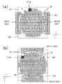
その例を図2(a)および図2(b)に示す。図2(a)はX方向に対向した保持部80X1と保持部80X2により基板Wを把持した状態を示し、図2(b)はY方向に対向した、保持部80Y1と保持部80Y2により基板Wを把持した状態を示すものである。ここで、保持部80X1、保持部80X2、保持部80Y1、保持部80Y2は、基板Wの周縁部を把持する保持部80として機能するものである。
ところで、基板Wの周縁部を把持する保持部80を用いたとしても、バックアップステージ4と保持部80が干渉するケースがある。例えば、図2(b)のように保持部80Y1と保持部80Y2で基板Wを把持した場合、領域A1(領域A3)に仮固定されている半導体チップCを熱圧着しようとすると、バックアップステージ4と保持部80Y1(保持部80Y2)が干渉する箇所がある。一方、図2(a)のように保持部80X1と保持部80X2で基板を把持した場合も、基板W外周部付近の半導体チップCを熱圧着しようとすると、バックアップステージ4と保持部80X1(保持部80X2)が干渉することがある。
ところが、図2(b)で保持部80Y1または保持部80Y2とバックアップステージ4が干渉する可能性のあった領域A1および領域A3は、図2(a)のように保持部80X1と保持部80X2で基板Wを把持すれば、バックアップステージ4が保持部80X1および保持部80X2と干渉することなく、半導体チップCを熱圧着することができる。また、図2(b)の保持部配置であれば、A2の領域内でバックアップステージ4が保持部80Y1と保持部80Y2の何れとも干渉することなく、半導体チップCを熱圧着することができる。すなわち、基板Wの半導体チップCを熱圧着する過程において、基板Wを把持する保持部80の位置を変更することにより、基板外周部付近に仮固定されたものに至るまでの全ての半導体チップCの熱圧着することが可能になる。しかも、ボンディングヘッド7の押圧面とバックアップステージ4の面形状は1対1で対応しているので、基板W内の仮固定位置に係わらず、同一の平行度で熱圧着を行うことができる。
なお、図2においては、2つの保持部80を対向するよう配置して、基板Wを把持する位置を1回変更することで、基板Wの全ての半導体チップCを熱圧着することを可能としているが、保持部80の数および基板Wを把持する位置の変更回数はこれに限定されるものではない。基板Wが大きければ3個以上の保持部80が基板Wを同時に把持しても良く、基板W把持する位置の変更は2回以上でもよい。また、基板Wを同時に把持する保持部80の一部のみを位置変更しても良い。
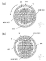
次に、本実施形態において、図2のように対向配置した保持部80が基板Wを把持する位置を変更する機構の一例について説明する。図3(a)は、リング8Rの内側に保持部80として機能する保持部80Aおよび保持部80Bが形成されたものである。図3(a)の状態では、図2(a)の保持部80X1に保持部80Aが相当し、保持部80X2に保持部80Bが相当しているが、80Rが回転することで図3(b)のようになり、保持部80Aが図3(b)の保持部80Y1(または保持部80Y2)に相当し、保持部80Bが保持部80Y2(または保持部80Y1)に相当するようになる。
ところで、保持部80Aおよび保持部80Bが基板Wを把持した状態でリング8Rが回転すると基板Wも回転してしまうが、本実施形態では基板Wは回転させずにリング8Rを回転させ、保持部80Aおよび保持部80Bによる把持位置を変える機構となっている。そこで、その具体的な構成および動作の一例について、図4から図6を用いて説明する。
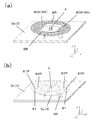
図4(a)はX方向可動部3b上に配置された、保持部80Aおよび保持部80Bを有するリング8Rの外観を示す図であり、図4(b)はリング8RとX方向可動部3bの間にある構成要素を示す透視図である。
図4(b)において、X方向可動部3b上に高さ調整機構81が複数固定配置され、高さ調整機構81はピン81Pの高低による高さ調整が可能である。また、リング8Rには、ピン83Pが複数個固定されている。このピン83Pは、図5に周辺部の断面図を示すように、θ方向可動部3cに固定された筒部83に対して上下方向に摺動可能に設けられている。また、ピン83Pは、X方向可動部3b上に固定配置された高さ調整機構82のピン82Pにより、下から突上げられるように配置されている。
ここで、高さ調整機構81および高さ調整機構82は、高さが「高」か「低」の何れかに固定されるものである。また、θ方向可動部3cは回転体3Rの駆動により回転角(θ方向)の調整が可能になっている。なお、図4(b)において回転体3Rは円柱形状になっているが、歯車によってθ方向可動部3cの回転角を調整するギア機構であってもよい。
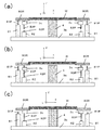
図4の構成を、バックアップステージ4を含めて、Y方向から見た断面図としたものが図6であり、図6(a)から図6(c)は動作状態の違いを示している。
図6(a)は熱圧着動作が行える状態を示したものであり、高さ調整機構81が「高」で、高さ調整機構82が「低」となっており、リング8Rを高さ調整機構81が支え、保持部80Aおよび保持部80Bが基板Wを把持した状態である。この状態で基板Wの裏面は、バックアップステージ4の高さとなる。すなわち、基板Wはバックアップステージ4に支持された状態となり、ボンディングヘッド7の下降により熱圧着が行える。
図6(b)は、基板Wが水平移動可能な状態を示したものであり、高さ調整機構82が「高」で、高さ調整機構81が「高」となっており、リング8Rを高さ調整機構82がピン83Pを介してが支え、保持部80Aおよび保持部80Bが基板Wを把持した状態である。この状態では基板Wの裏面は、バックアップステージ4上面より高くなる。このため、ボンディングヘッド7が上昇した状態であるならば、保持部80Aおよび保持部80Bに基板Wは把持されているので、Y方向可動部3aとX方向可動部3bによる水平移動に伴って、保持部80Aおよび保持部80Bに把持された基板Wを水平移動させることができる。なお、図6(a)の状態でバックアップステージ4が基板Wを吸着保持している場合は、吸着を解除してから、図6(b)の状態に移行する必要がある。また、図6(b)では高さ調整機構81が「高」となっているが、高さ調整機構82が「高」の状態であれば、高さ調整機構81は「低」でもよい。
図6(b)は、基板Wが水平移動可能な状態を示したものであり、高さ調整機構82が「高」で、高さ調整機構81が「高」となっており、リング8Rを高さ調整機構82がピン83Pを介してが支え、保持部80Aおよび保持部80Bが基板Wを把持した状態である。この状態では基板Wの裏面は、バックアップステージ4上面より高くなる。このため、ボンディングヘッド7が上昇した状態であるならば、保持部80Aおよび保持部80Bに基板Wは把持されているので、Y方向可動部3aとX方向可動部3bによる水平移動に伴って、保持部80Aおよび保持部80Bに把持された基板Wを水平移動させることができる。なお、図6(a)の状態でバックアップステージ4が基板Wを吸着保持している場合は、吸着を解除してから、図6(b)の状態に移行する必要がある。また、図6(b)では高さ調整機構81が「高」となっているが、高さ調整機構82が「高」の状態であれば、高さ調整機構81は「低」でもよい。
図6(c)は、リング8Rが回転可能な状態を示したものであり、高さ調整機構81、高さ調整機構82がともに「低」の状態で、リング8Rは高さ調整機構81に支持されず、高さ調整機構82のピン82Pの先端は、リング80Rに固定されたピン83Pに接触していない。このため、リング80Rは、Y方向可動部3bとの機械的接続が解除され、θ方向可動部3c上に固定された状態となる。この状態では、バックアップステージ4に支持される基板Wよりリング8Rが低くなっており、保持部80Aおよび保持部80Bともに基板Wを把持していない。このため、固定状態の基板Wに対し、θ方向可動部3cの駆動によりリング8Rが回転して、保持部80Aおよび保持部80Bの位置が基板Wの縁に沿って動く。リング8Rが所定角度(例えば90°)回転した段階でθ方向可動機構3cを停止すれば、図3(a)から図3(b)のような位置変化となる。ここで、回転後にも、ピン83Pの直下に高さ調整機構82が存在するように、Y方向可動部3b上に高さ調整機構82を複数配置しておく必要がある。
なお、リング8Rの回転を行う際、基板Wはバックアップステージ4のみによって保持される。このため、図6(c)の状態にする際は、バックアップステージ4が基板Wの重心直下付近となるように、図6(b)の状態から基板Wの位置調整を行うことが望ましい。また、リング8Rを回転させる際には、バックアップステージ4が基板Wを吸着保持することが望ましい。
図6(c)の状態でリング8Rを所定角度回転させた後は、高さ調整機構81を「高」にすれば、保持部80Aおよび保持部80Bの位置が変更された状態で基板Wを把持することができる。
なお。図6において、保持部80Aおよび保持部80Bが基板Wを把持する際に、マイクロ吸盤機構や粘着物質を用いて把持力を強めることが望ましいが、図7のようにリング8R内に吸気手段9に連通する吸気ライン8Lを設けてもよい。吸気ライン8Lを用いることで、図7(a)および図7(b)のように保持部80Aおよび保持部80Bが基板Wを把持する際に吸着力を強める一方で、吸気手段9の機能を停止することで、図7(c)の状態に移行する際の保持部80Aおよび保持部80Bによる把持を容易に解除することも可能になる。
本実施形態において、便宜的に保持部80Aと保持部80Bと記したが、何れも同じ形状であっても良いが、異なる形状であっても良い。また、本実施形態において、保持部80Aおよび保持部80Bを含むリング8R、高さ調整機構81、高さ調整機構82およびピン83P等によって基板把持手段8は構成されているが、これに限定されるものではなく、例えば、高さ調整機構82として、位置制御可能な1軸の駆動手段を用いることで基板Wを把持する高さを微調整する構成とすれば高さ調整機構81を不要とすることも可能である。
更に、図4では一組の保持部80を移動させて把持位置を変更させる構成としているが、別な構成として、複数組の保持部80から、基板を把持する保持部80の組み合わせを変える構成としてもよい。
その一例を図8および図9を用いて説明する。図8では、基板把持手段8は保持部80a、保持部80b、保持部80cおよび保持部80dの4つの保持部80を有するものである。図9は、この4つの保持部80を、保持部80aと保持部80bの組み合わせと、保持部80cと保持部80dの組合わせに分け、図2のように基板Wの把持位置を変更するものである。この構成においては、基板把持手段8は保持部80(保持部80a~保持部80d)の高さ調整機能とともに、基板Wを把持しない保持部80(保持部80aと保持部80bの組み合わせ、または保持部80cと保持部80dの組み合わせの何れか)を基板W周縁部から退避させる機能を有している必要がある。なお、図8のように4つの保持部80を有する場合において、基板Wを同時に把持する保持部80の組合わせは図9に限定されるものではなく、保持部80aと保持部80cの組み合わせと、保持部80bと保持部80dの組合わせであってもよい。図8のような構成にすることにより、図1におけるθ方向可動部3cを省くことも可能となる。
なお、図4および図8の何れの構成においても、ボンディングヘッド7とバックアップステージ4に対する基板W上の半導体チップCの位置関係は、水平回りの回転方向を変えずに熱圧着出来るので、ボンディングヘッド7やバックアップステージ4に複雑な回転機構が不要となり、剛性も高められる。
以上の実施形態で説明したように、本発明を用いることにより、基板に仮固定された半導体チップを熱圧着するのに際して、基板外周部付近に仮固定された半導体チップに至るまで均一な条件で熱圧着を行うことができる。
ところで、ここまでは、基板に仮固定された半導体チップを熱圧着する仮本分割プロセスを前提として説明してきたが、本発明はボンディングヘッドが1つ1つの半導体チップを基板の所定箇所に配置して熱圧着まで行うプロセス(以下「一貫プロセス」と記す)においても有効である。すなわち、半導体チップを基板に加圧する押圧面を有するボンディングヘッドと、押圧面によって加圧される領域を基板の裏面から支持するバックアップステージの組み合わせで実装を行うのであれば、一貫プロセスにおいても基板把持手段とバックアップステージの干渉は課題として存在し、本発明によって解決される。
1 実装装置
2 基台
3 XYθ可動機構
3a Y方向可動部
3b X方向可動部
3θ θ方向可動部
4 バックアップステージ
5 フレーム
6 圧着ユニット
7 ボンディングヘッド
8 基板把持手段
8R リング
9 吸気手段
80、80A、80B、80a、80b、80c、80d、80X1、80X2、80Y1、80Y2 保持部
81 高さ調整機構
81P ピン
82 高さ調整機構
82P ピン
83P ピン
C 半導体チップ
W 基板
2 基台
3 XYθ可動機構
3a Y方向可動部
3b X方向可動部
3θ θ方向可動部
4 バックアップステージ
5 フレーム
6 圧着ユニット
7 ボンディングヘッド
8 基板把持手段
8R リング
9 吸気手段
80、80A、80B、80a、80b、80c、80d、80X1、80X2、80Y1、80Y2 保持部
81 高さ調整機構
81P ピン
82 高さ調整機構
82P ピン
83P ピン
C 半導体チップ
W 基板
Claims (4)
- 基板に半導体チップを熱圧着する実装装置であって、
半導体チップを基板に加圧する押圧面を有するボンディングヘッドと、
前記押圧面によって加圧される領域を、前記基板の裏面から支持するバックアップステージと、
前記基板の周縁部を保持部を用いて部分的に把持する基板把持手段とを備え、
前記基板把持手段が前記基板を把持する前記保持部の位置を変更する機能を有する実装装置。 - 請求項1に記載の実装装置であって、
前記基板把持手段が前記保持部の位置を基板の周縁に沿って移動させて、前記基板を把持する位置を変える機能を有した実装装置。 - 請求項1に記載の実装装置であって、
前記基板把持手段が、前記保持部を複数有し、
複数の保持部の一部のみに前記基板の周縁部を把持させ、
他の保持部は前記基板の周縁部から退避させる機能を有する実装装置。 - 基板に仮固定された半導体チップを熱圧着する実装方法であって、
前記半導体チップを加熱圧着するボンディングヘッドと、前記ボンディングヘッドと一対となって前記基板を裏面から支持するバックアップステージを用い、
前記基板の周縁部を部分的に把持する基板把持手段によって前記基板を移動させながら、前記基板上に半導体チップを順次熱圧着する過程において、
前記基板把持手段が基板を把持する位置の変更を少なくとも1回行う実装方法。
Priority Applications (2)
| Application Number | Priority Date | Filing Date | Title |
|---|---|---|---|
| CN201780040004.4A CN109417038A (zh) | 2016-06-28 | 2017-06-15 | 安装装置和安装方法 |
| KR1020187037441A KR102340087B1 (ko) | 2016-06-28 | 2017-06-15 | 실장 장치 및 실장 방법 |
Applications Claiming Priority (2)
| Application Number | Priority Date | Filing Date | Title |
|---|---|---|---|
| JP2016-127523 | 2016-06-28 | ||
| JP2016127523A JP6663805B2 (ja) | 2016-06-28 | 2016-06-28 | 実装装置および実装方法 |
Publications (1)
| Publication Number | Publication Date |
|---|---|
| WO2018003519A1 true WO2018003519A1 (ja) | 2018-01-04 |
Family
ID=60786640
Family Applications (1)
| Application Number | Title | Priority Date | Filing Date |
|---|---|---|---|
| PCT/JP2017/022117 Ceased WO2018003519A1 (ja) | 2016-06-28 | 2017-06-15 | 実装装置および実装方法 |
Country Status (4)
| Country | Link |
|---|---|
| JP (1) | JP6663805B2 (ja) |
| KR (1) | KR102340087B1 (ja) |
| CN (1) | CN109417038A (ja) |
| WO (1) | WO2018003519A1 (ja) |
Cited By (1)
| Publication number | Priority date | Publication date | Assignee | Title |
|---|---|---|---|---|
| CN117438371A (zh) * | 2023-12-22 | 2024-01-23 | 天津中科晶禾电子科技有限责任公司 | 下压头单体、压接组件、芯片烧结炉 |
Families Citing this family (1)
| Publication number | Priority date | Publication date | Assignee | Title |
|---|---|---|---|---|
| CN114999961B (zh) * | 2022-06-06 | 2026-02-27 | 安徽龙芯微科技有限公司 | 一种基于可视化的半导体芯片封装方法及系统 |
Citations (1)
| Publication number | Priority date | Publication date | Assignee | Title |
|---|---|---|---|---|
| JP2009267413A (ja) * | 2008-04-25 | 2009-11-12 | Sts Semiconductor & Telecommunications Co Ltd | 幅広リードフレーム用の半導体パッケージ製造装置及びこれを利用した半導体パッケージの製造方法 |
Family Cites Families (11)
| Publication number | Priority date | Publication date | Assignee | Title |
|---|---|---|---|---|
| JPH06232241A (ja) * | 1993-02-03 | 1994-08-19 | Matsushita Electric Ind Co Ltd | 半導体製造装置の基板位置決め機構 |
| JPH11165864A (ja) * | 1997-12-03 | 1999-06-22 | Nikon Corp | 基板搬送装置及び基板処理装置 |
| JP3832982B2 (ja) * | 1998-10-09 | 2006-10-11 | 株式会社ハイメック | ウエハ目視検査装置 |
| KR100695233B1 (ko) * | 2005-11-23 | 2007-03-14 | 세메스 주식회사 | 기판 세정 장치 및 방법 |
| US8025829B2 (en) * | 2006-11-28 | 2011-09-27 | Nanonex Corporation | Die imprint by double side force-balanced press for step-and-repeat imprint lithography |
| JP5760212B2 (ja) * | 2008-06-12 | 2015-08-05 | 株式会社アドウェルズ | 実装装置および実装方法 |
| JP5780445B2 (ja) * | 2011-01-24 | 2015-09-16 | 株式会社東京精密 | 半導体ウエーハブレーキング装置及び方法 |
| JP2013239563A (ja) * | 2012-05-15 | 2013-11-28 | Disco Abrasive Syst Ltd | ウェーハの分割方法 |
| JP6151925B2 (ja) * | 2013-02-06 | 2017-06-21 | ヤマハ発動機株式会社 | 基板固定装置、基板作業装置および基板固定方法 |
| JP6234277B2 (ja) | 2014-03-05 | 2017-11-22 | 東レエンジニアリング株式会社 | 圧着ヘッド、それを用いた実装装置および実装方法 |
| JP6382049B2 (ja) | 2014-09-29 | 2018-08-29 | 三菱日立パワーシステムズ環境ソリューション株式会社 | 電気集塵装置補強構造及び電気集塵装置 |
-
2016
- 2016-06-28 JP JP2016127523A patent/JP6663805B2/ja active Active
-
2017
- 2017-06-15 WO PCT/JP2017/022117 patent/WO2018003519A1/ja not_active Ceased
- 2017-06-15 KR KR1020187037441A patent/KR102340087B1/ko active Active
- 2017-06-15 CN CN201780040004.4A patent/CN109417038A/zh active Pending
Patent Citations (1)
| Publication number | Priority date | Publication date | Assignee | Title |
|---|---|---|---|---|
| JP2009267413A (ja) * | 2008-04-25 | 2009-11-12 | Sts Semiconductor & Telecommunications Co Ltd | 幅広リードフレーム用の半導体パッケージ製造装置及びこれを利用した半導体パッケージの製造方法 |
Cited By (1)
| Publication number | Priority date | Publication date | Assignee | Title |
|---|---|---|---|---|
| CN117438371A (zh) * | 2023-12-22 | 2024-01-23 | 天津中科晶禾电子科技有限责任公司 | 下压头单体、压接组件、芯片烧结炉 |
Also Published As
| Publication number | Publication date |
|---|---|
| KR102340087B1 (ko) | 2021-12-15 |
| CN109417038A (zh) | 2019-03-01 |
| KR20190021262A (ko) | 2019-03-05 |
| JP2018006402A (ja) | 2018-01-11 |
| JP6663805B2 (ja) | 2020-03-13 |
Similar Documents
| Publication | Publication Date | Title |
|---|---|---|
| JP4821091B2 (ja) | ウェハの接合装置 | |
| CN110226220B (zh) | 接合装置和接合方法 | |
| US11189594B2 (en) | Bonding apparatus and bonding method | |
| JP2005045168A (ja) | インプリント方法およびインプリント装置 | |
| JP2017183481A (ja) | 実装装置および実装方法 | |
| JP6816992B2 (ja) | 実装装置 | |
| WO2018003519A1 (ja) | 実装装置および実装方法 | |
| TWI397970B (zh) | 提供大鍵合力的旋轉鍵合工具 | |
| TWI480968B (zh) | 用於提供大鍵合力的晶粒鍵合機 | |
| JPWO2015075832A1 (ja) | ボンディング装置およびボンディング方法 | |
| KR20170121909A (ko) | 웨이퍼 상에 다이들을 본딩하기 위한 장치 및 방법 | |
| JP6789791B2 (ja) | 半導体装置の製造装置および製造方法 | |
| KR101421574B1 (ko) | 웨이퍼 접합 시스템용 웨이퍼 쿨러 언클램핑 조립체 | |
| KR101090816B1 (ko) | 반도체 칩 본딩장치 | |
| JP2020107640A (ja) | 実装装置および実装方法 | |
| JP6863767B2 (ja) | 実装装置および実装方法 | |
| WO2023136076A1 (ja) | 位置決め装置およびこれを用いた実装装置 | |
| KR102252734B1 (ko) | 다이 본딩 장치 | |
| JP3400735B2 (ja) | 傾き調整装置およびボンディング装置 | |
| JP2009059961A (ja) | ダイボンダー装置 | |
| KR102220338B1 (ko) | 칩 본딩 장치 및 방법 | |
| JP7778349B2 (ja) | 電子部品接合装置 | |
| CN113764311B (zh) | 转角平台机构 | |
| US20230290666A1 (en) | Semiconductor manufacturing apparatus, carrier jig, and manufacturing method of semiconductor device | |
| CN121335483A (zh) | 一种激光解键合设备及键合晶圆分离机械手 |
Legal Events
| Date | Code | Title | Description |
|---|---|---|---|
| 121 | Ep: the epo has been informed by wipo that ep was designated in this application |
Ref document number: 17819879 Country of ref document: EP Kind code of ref document: A1 |
|
| ENP | Entry into the national phase |
Ref document number: 20187037441 Country of ref document: KR Kind code of ref document: A |
|
| NENP | Non-entry into the national phase |
Ref country code: DE |
|
| 122 | Ep: pct application non-entry in european phase |
Ref document number: 17819879 Country of ref document: EP Kind code of ref document: A1 |