WO2018003262A1 - 複合基板及び複合基板の製造方法 - Google Patents
複合基板及び複合基板の製造方法 Download PDFInfo
- Publication number
- WO2018003262A1 WO2018003262A1 PCT/JP2017/016313 JP2017016313W WO2018003262A1 WO 2018003262 A1 WO2018003262 A1 WO 2018003262A1 JP 2017016313 W JP2017016313 W JP 2017016313W WO 2018003262 A1 WO2018003262 A1 WO 2018003262A1
- Authority
- WO
- WIPO (PCT)
- Prior art keywords
- metal conductor
- ceramic
- ceramic layer
- layer
- composite substrate
- Prior art date
- Legal status (The legal status is an assumption and is not a legal conclusion. Google has not performed a legal analysis and makes no representation as to the accuracy of the status listed.)
- Ceased
Links
Images


Classifications
-
- H—ELECTRICITY
- H05—ELECTRIC TECHNIQUES NOT OTHERWISE PROVIDED FOR
- H05K—PRINTED CIRCUITS; CASINGS OR CONSTRUCTIONAL DETAILS OF ELECTRIC APPARATUS; MANUFACTURE OF ASSEMBLAGES OF ELECTRICAL COMPONENTS
- H05K3/00—Apparatus or processes for manufacturing printed circuits
- H05K3/46—Manufacturing multilayer circuits
Definitions
- the present invention relates to a composite substrate and a method for manufacturing the composite substrate.
- Patent Document 1 discloses a laminate having a dielectric layer formed of a high dielectric constant material containing lead oxide as a main component and a low dielectric constant insulating layer formed of a material having a dielectric constant lower than that of the high dielectric constant material. A method of manufacturing a multilayer ceramic substrate that is co-fired is described.
- a low dielectric constant green sheet made of a low dielectric constant material and a high dielectric constant green sheet made of a high dielectric constant material are respectively produced.
- a multilayer ceramic substrate is manufactured by laminating a low dielectric constant green sheet and a high dielectric constant green sheet, thermocompression bonding, and firing.
- the low dielectric constant green sheet and the high dielectric constant green sheet are in direct contact. If firing is performed in a state where the green sheets made of different materials are in direct contact, warpage or delamination may occur when the temperature is raised or lowered due to the difference in thermal expansion coefficient of the different materials. Therefore, it is necessary to make the thermal expansion coefficients of different materials close to each other. In addition, mutual diffusion occurs at the interface where different materials are in contact with each other, and the respective materials may react to change the electrical characteristics.
- the present invention has been made to solve the above problems, and is a composite substrate including a ceramic layer made of a different material, and has a high degree of freedom in selecting a ceramic material as a different material and is easy to manufacture.
- An object of the present invention is to provide a composite substrate and a manufacturing method thereof.
- the present inventor has found that the above-mentioned problems can be solved by directly firing the ceramic layers made of different materials without bringing them into direct contact with each other, and has completed the present invention.
- the composite substrate of the present invention comprises a first ceramic layer made of a first ceramic material and a second ceramic material having a composition different from that of the first ceramic material, and is in direct contact with the first ceramic layer.
- a composite substrate comprising a second ceramic layer not formed and a metal conductor portion located between the first ceramic layer and the second ceramic layer, wherein the first ceramic layer and the second ceramic layer
- the ceramic layer is provided with a metal conductor for interlayer connection, and the metal conductor portion is integrated with the metal conductor in the first ceramic layer and the metal conductor in the second ceramic layer.
- the composite substrate of the present invention includes a first ceramic material and a second ceramic material, which are different materials, respectively, but the first ceramic layer and the second ceramic layer are not in direct contact with each other. Therefore, there is no problem caused by direct contact between the ceramic layers made of different materials. Therefore, a combination of ceramic materials having a large difference in thermal expansion coefficient can be selected as the different material, and the degree of freedom in selecting the ceramic material as the different material can be increased.
- a metal conductor portion is provided between the first ceramic layer and the second ceramic layer, and the first ceramic layer and the second ceramic layer are integrated by the metal conductor portion. Specifically, the metal conductor in the first ceramic layer, the metal conductor in the second ceramic layer, and the metal conductor portion therebetween are integrated. With such a configuration, the metal conductor in the first ceramic layer, the metal conductor in the second ceramic layer, and the metal conductor portion therebetween can be easily aligned, so that a fine connection is achieved. It becomes easy to manufacture a composite substrate having
- the metal conductor and the metal conductor portion are integrated means that the intermetallic bonding state between the metal conductor of the first ceramic layer and the metal conductor portion, and the second ceramic layer. This means that the intermetallic bonding state between the metal conductor and the metal conductor portion is the same.
- the metal-to-metal bonding state of the metal conductors between the plurality of ceramic layers is the same.
- a composite substrate in which the metal conductor of the ceramic layer and the metal conductor portion between the ceramic layers are integrated is difficult to obtain by a method in which substrates made of different ceramic materials are separately fired and bonded.
- first ceramic layer and the second ceramic layer when the first ceramic layer and the second ceramic layer are not distinguished from each other, they may be simply referred to as “ceramic layer”, and the first ceramic material and the second ceramic material are distinguished from each other. When not, it may be described simply as “ceramic material”.
- the content ratio of alumina is higher in the surface portion on the metal conductor portion side of the first ceramic layer than in the central portion of the first ceramic layer. Moreover, it is preferable that the content rate of an alumina is higher than the center part of the said 2nd ceramic layer in the surface part by the side of the said metal conductor part of the said 2nd ceramic layer.
- a preferred method for producing the composite substrate of the present invention there is a method of firing by sandwiching a cavity forming sheet having alumina as a cavity forming material between a first ceramic green sheet and a second ceramic green sheet. .
- the content ratio of alumina is increased in the surface portions on the metal conductor portion side of the first ceramic layer and the second ceramic layer.
- the first ceramic layer and the second ceramic layer function as a protective layer for preventing elution of glass components contained in the ceramic layer. Therefore, the mechanical strength of the surface of the first ceramic layer and the second ceramic layer on the metal conductor portion side can be increased.
- a space between the first ceramic layer and the second ceramic layer is a resin layer including the metal conductor portion.
- the resin layer works as a stress relaxation layer, and therefore, a composite substrate having a higher strength against impact than the case without the resin layer, can do.
- a functional resin layer using a functional resin material in the resin layer, characteristics that are difficult to achieve with a ceramic material can be imparted to the composite substrate.
- hard low dielectric constant achieved by the ceramic material for example, specific dielectric constant epsilon r is 2 or less
- a resin material it is possible to reduce the transmission loss in a high frequency range.
- the distance between the first ceramic layer and the second ceramic layer is preferably 5 ⁇ m or more and 200 ⁇ m or less.
- the distance between the first ceramic layer and the second ceramic layer is 5 ⁇ m or more, the first ceramic material and the second ceramic material are disposed between the first ceramic layer and the second ceramic layer in the firing step. Even if it diffuses, the space between the first ceramic layer and the second ceramic layer is prevented from being filled with a dense material. Therefore, it is possible to prevent cracks from being generated between the first ceramic layer and the second ceramic layer in the firing step.
- the distance between the first ceramic layer and the second ceramic layer is 200 ⁇ m or less, the height of the metal conductor portion does not become too high, and therefore the first ceramic layer and the second ceramic layer are formed by the metal conductor portion. And a composite substrate having a necessary mechanical strength.
- the relative dielectric constant ⁇ r1 of the first ceramic material is lower than the relative dielectric constant ⁇ r2 of the second ceramic material.
- the metal material contained in the metal conductor portion is preferably copper. Copper is suitable as a material constituting the metal conductor portion because of its high conductivity. Moreover, since it is a soft metal, when it uses for a metal conductor part, since the stress which arises between dissimilar materials can be relieved, it is preferable.
- the proportion of the metal material contained in the metal conductor portion is preferably 40% by weight to 99% by weight.
- the ratio of the metal material is 99% by weight or less, that is, the presence of a material other than the metal material (ceramic material or the like)
- the metal conductor portion has a strong bonding state with the metal conductor for interlayer connection in the ceramic layer.
- the composite substrate can be formed and has higher strength against impact.
- the ratio (% by weight) of the metal material contained in the metal conductor portion and the metal material contained in the metal conductor for interlayer connection in the first ceramic layer and the second ceramic layer is preferably 59% by weight or less. If the difference in the proportion of the metal material is 59% by weight or less, the metal conductor portion and the metal conductor for interlayer connection in the ceramic layer have the same characteristics, and the sintering behavior, thermal expansion characteristics and strength are the same. Therefore, the bonding between the metal conductor portion and the metal conductor can be made stronger. As a result, a composite substrate having higher strength against impact can be obtained.
- the ratio of the metal material contained in the metal conductor is different between the metal conductor for interlayer connection in the first ceramic layer and the metal conductor for interlayer connection in the second ceramic layer, the average value thereof is calculated. I will do it.
- the method for producing a composite substrate of the present invention includes a first ceramic green sheet made of an unsintered first ceramic material and having a metal conductor paste for interlayer connection, and a composition different from the first ceramic material.
- a second ceramic green sheet made of a sintered second ceramic material and having a metal conductor paste for interlayer connection, and a metal conductor portion forming sheet having a metal conductor paste for interlayer connection are formed as described above.
- the metal conductor paste in the first ceramic green sheet, the second ceramic, The metal conductor paste in the green sheet and the metal conductor paste in the metal conductor part forming sheet are integrally sintered to form a metal conductor and a metal conductor part for interlayer connection, and the unsintered first And firing the ceramic material and the unsintered second ceramic material to form a first ceramic layer and a second ceramic layer.
- the metal conductor paste formed in each layer can be aligned before firing. it can.
- the metal conductor paste formed in each layer is sintered simultaneously.
- the metal conductor of the first ceramic layer, the metal conductor portion, and the metal conductor of the second ceramic layer are integrated to ensure bonding strength. Therefore, a composite substrate with high connection reliability can be manufactured.
- the firing step by placing a constraining layer on each of the upper and lower main surfaces of the laminate.
- the constraining layers are arranged on the upper and lower main surfaces of the laminated body, shrinkage in the planar direction of the laminated body can be suppressed in the firing step. Therefore, the dimensional accuracy of the composite substrate can be increased.
- the material constituting the constraining layer is preferably alumina.
- Alumina is suitable as a material for the constraining layer because it does not sinter at the firing temperature in the firing step and does not easily react with the ceramic material contained in the ceramic green sheet.
- the metal conductor portion forming sheet includes a first cavity forming material that does not sinter or burn out at the firing temperature, and a metal conductor paste for interlayer connection. It is preferable that a cavity be formed between the first ceramic layer and the second ceramic layer by removing the first cavity forming material after the firing step.
- the first cavity forming material is preferably alumina.
- Firing is performed using the first cavity forming material, and only the metal conductor portion is left between the first ceramic layer and the second ceramic layer by removing the first cavity forming material after firing.
- the composite substrate of the present invention can be manufactured by forming a cavity. Since the first cavity forming material is a material that does not sinter or burn out at the firing temperature, it can be removed by ultrasonic treatment or the like. Alumina is a material that does not sinter or burn out at the above firing temperature, and is less likely to react with the ceramic material contained in the ceramic green sheet, and therefore is suitable as the first cavity forming material.
- the metal conductor portion forming sheet has a second cavity forming material having a second cavity forming material that burns down at the firing temperature and a metal conductor paste for interlayer connection. It is a sheet, and it is preferable to form a cavity between the first ceramic layer and the second ceramic layer by burning out the second cavity forming material in the firing step.
- the second cavity forming material is preferably carbon.
- the second cavity-forming material is a material that burns away at the firing temperature, and therefore, between the first ceramic layer and the second ceramic layer.
- the composite substrate of the present invention can be manufactured by leaving only the metal conductor portion and forming a cavity.
- Carbon is a material that burns out at the firing temperature and is less likely to react with the ceramic material contained in the ceramic green sheet, and is therefore suitable as the second cavity forming material.
- the composite substrate manufacturing method of the present invention it is preferable to further perform a resin layer forming step of forming a resin layer between the first ceramic layer and the second ceramic layer.
- the heat resistance temperature of the resin material is lower than the sintering temperature of the unsintered ceramic constituting the ceramic green sheet and the sintering temperature of the metal conductor paste, so even if a resin layer is provided before firing the ceramic green sheet, Although the material is burned out, a resin layer can be provided after firing the ceramic green sheet.
- the resin layer has a resin layer in which the metal conductor portion is integrated with the metal conductor for interlayer connection in the ceramic layer and firmly joined. A substrate can be manufactured.
- the composite substrate containing the ceramic layer which consists of a dissimilar material, Comprising: The composite substrate with a high freedom degree of selection of the ceramic material as a dissimilar material, and easy manufacture can be provided.
- FIG. 1 is a cross-sectional view schematically showing an example of the composite substrate of the present invention.
- FIG. 2 is a cross-sectional view schematically showing another example of the composite substrate of the present invention.
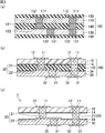
- FIG. 3A, FIG. 3B, and FIG. 3C are cross-sectional views schematically showing an example of the manufacturing process of the composite substrate of the present invention.
- FIG. 1 is a cross-sectional view schematically showing an example of the composite substrate of the present invention.
- the composite substrate 1 of the present invention includes a first ceramic layer 10, a second ceramic layer 30, and a composite including a metal conductor portion 20 located between the first ceramic layer 10 and the second ceramic layer 30. It is a substrate.
- the first ceramic layer 10 and the second ceramic layer 30 are not in direct contact, and the metal conductor portion 20 is sandwiched between the first ceramic layer 10 and the second ceramic layer 30.
- the first ceramic layer 10 has a first ceramic material as an insulating material and has a metal conductor 11 for interlayer connection.
- a metal wiring 12 is formed in the planar direction of the first ceramic layer 10 and is electrically connected to the metal conductor 11.
- the second ceramic layer 30 has a second ceramic material as an insulating material and has a metal conductor 31 for interlayer connection.
- a metal wiring 32 is formed in the planar direction of the second ceramic layer 30 and is electrically connected to the metal conductor 31.
- the second ceramic material is a material having a composition different from that of the first ceramic material.
- the metal conductor portion 20 is a metal conductor integrated with the metal conductor 11 for interlayer connection in the first ceramic layer 10 and the metal conductor 31 for interlayer connection in the second ceramic layer 30.
- the metal conductor portion 20 includes at least a metal conductor 21 for connection in the thickness direction.
- the right side of FIG. 1 shows a portion where the metal conductor 21 is a columnar metal conductor integrated with the metal conductor 11 and the metal conductor 31 in a straight line in the thickness direction. In this case, the metal conductor 21 is the metal conductor portion 20.
- the metal conductor portion 20 includes a metal wiring 22 that is electrically connected to the metal conductor 21 in addition to the metal conductor 21, and the metal conductor 21 contacts the metal conductor 11. Shows a portion in contact with the metal conductor 31 where the metal conductor 11, the metal conductor 21, the metal wiring 22, and the metal conductor 31 are integrated.
- the interlayer connection metal conductor 11 in the first ceramic layer 10 and the interlayer connection metal conductor 31 in the second ceramic layer 30 are integrated with the metal conductor portion 20 including the metal wiring 22.
- the metal conductor portion is included in the embodiment integrated with the metal conductor in the first ceramic layer and the metal conductor in the second ceramic layer.
- the first ceramic material constituting the first ceramic layer 10 and the second ceramic material constituting the second ceramic layer 30 are sintered ceramic materials.
- the first ceramic material and the second ceramic material are ceramic materials having different compositions. Therefore, different characteristics can be exhibited in the first ceramic layer and the second ceramic layer.
- the first ceramic material and the second ceramic material preferably include a low-temperature sintered ceramic material.
- the low-temperature sintered ceramic material means a material that can be sintered at a firing temperature of 1000 ° C. or less and can be simultaneously fired with silver or copper, which is preferably used as a metal material.
- the low-temperature sintered ceramic material is a glass composite low-temperature sintered ceramic material obtained by mixing borosilicate glass with a ceramic material such as quartz, alumina, forsterite, or the like, ZnO—MgO—Al 2 O 3 — Crystallized glass-based low-temperature sintered ceramic materials using SiO 2 -based crystallized glass, BaO—Al 2 O 3 —SiO 2 ceramic materials and Al 2 O 3 —CaO—SiO 2 —MgO—B 2 O 3 systems
- a non-glass type low-temperature sintered ceramic material using a ceramic material or the like can be used.
- the first ceramic material and the second ceramic material may include a magnetic material such as ferrite and a piezoelectric material such as PZT (lead zirconate titanate) in addition to the low-temperature sintered ceramic material. .
- a magnetic material such as ferrite
- a piezoelectric material such as PZT (lead zirconate titanate)
- the first ceramic material and the second ceramic material are low-temperature sintered ceramic materials, and are preferably a combination of a low dielectric constant material and a high dielectric constant material.
- the relative dielectric constant ⁇ r1 of the first ceramic material is preferably lower than the relative dielectric constant ⁇ r2 of the second ceramic material.
- the relative dielectric constant ⁇ r1 of the first ceramic material as the low dielectric constant material is More preferably, the relative dielectric constant ⁇ r2 of the second ceramic material as the high dielectric constant material is 10 or less.
- Si is converted into SiO 2 in a range of 48% to 75% by weight
- Ba is converted into BaO in a range of 20% to 40% by weight
- Al is converted into Al 2 O 3 .
- Mn is converted to MnO by 2 to 10 parts by weight
- Ti and Fe A subcomponent ceramic material containing 0.1 to 10 parts by weight in terms of TiO 2 and Fe 2 O 3 , respectively, and substantially comprising Cr oxide and B oxide The material which does not contain any is mentioned.
- the subcomponent ceramic material is preferably a material containing 0.1 to 5 parts by weight of Mg in terms of MgO with respect to 100 parts by weight of the main component ceramic material. Further, as the subcomponent ceramic material, at least one selected from Nb, Ce, Zr and Zn is converted into Nb 2 O 5 , CeO 2 , ZrO 2 and ZnO with respect to 100 parts by weight of the main component ceramic material. A material containing 0.1 parts by weight or more and 6 parts by weight or less is preferable.
- the high dielectric constant material a material in which glass (borosilicate glass) is added to ceramic mainly composed of BaTiO 3 is preferable.
- first ceramic layer and the second ceramic layer may be configured by laminating a plurality of layers. Good.
- the first ceramic layers and the second ceramic layers may be in direct contact with each other, and a metal conductor for interlayer connection is provided between the ceramic layers to form a multilayer substrate.
- the composite substrate of the present invention may be provided with a third ceramic layer containing a third ceramic material having a composition different from that of the first ceramic material and the second ceramic material.
- the third ceramic layer is not in direct contact with the first ceramic layer and the second ceramic layer, and between the third ceramic layer and the first ceramic layer and the second ceramic layer. Further, it is preferable that the metal conductor portion is located.
- the content ratio of alumina is preferably higher than the center portion of the ceramic layer. 1 is hatched to schematically show the positions of the surface portion 14 of the first ceramic layer 10 on the metal conductor portion side and the surface portion 34 of the second ceramic layer 30 on the metal conductor portion side. .
- the “surface portion on the metal conductor portion side of the ceramic layer” means a region from the outermost surface located on the metal conductor portion side of the ceramic layer to a thickness of 1/10 in the thickness direction of the ceramic layer.
- the ceramic layer is composed of a plurality of layers, only the ceramic layer located closest to the metal conductor portion is meant.
- the definition is the same in the first ceramic layer and the second ceramic layer.
- the “center portion of the ceramic layer” means a region from the surface where the thickness of the ceramic layer is halved to a thickness of 1/20 in the thickness direction of the ceramic layer toward the metal conductor portion side, and on the side opposite to the metal conductor portion. In the meantime, it means a region obtained by combining regions up to 1/20 in the thickness direction of the ceramic layer. However, when the ceramic layer is composed of a plurality of layers, it means the central portion of the ceramic layer located closest to the metal conductor portion.
- the content ratio of alumina in the ceramic layer is the area ratio of the area where alumina exists by performing mapping analysis using FE-WDX (device name: JXA-8530F manufactured by JEOL Ltd.) on the measurement target area. Is calculated by obtaining.
- the content ratio of alumina is higher than the central portion of the ceramic layer also in the surface portion of the ceramic layer located on the outermost side of the composite substrate.
- the “surface portion of the ceramic layer located on the outermost side of the composite substrate” means a region from the outermost surface of the ceramic layer located on the outermost side of the composite substrate to a thickness of 1/10 in the thickness direction of the ceramic layer. The definition is the same in the first ceramic layer and the second ceramic layer.
- the material constituting the metal conductor portion and the metal conductor for interlayer connection in the ceramic layer is preferably a mixture of a metal material and a ceramic material.
- the metal material preferably includes at least one selected from gold, silver, and copper, and more preferably includes silver or copper. Since gold, silver, and copper have low resistance, they are particularly suitable when the composite substrate is used for high frequency. Moreover, since copper has high electrical conductivity, it is suitable as a metal material constituting the metal conductor portion. Moreover, since it is a soft metal, when it uses for a metal conductor part, since the stress which arises between dissimilar materials can be relieved, it is preferable.
- the same ceramic material as that constituting the ceramic layer can be suitably used.
- the sintering behavior of the ceramic material constituting the ceramic layer and the metal conductor paste can be matched.
- the ratio of the metal material contained in the metal conductor portion is preferably 40% by weight or more and 99% by weight or less, more preferably 60% by weight or more, and more preferably 90% by weight or less. That the ratio of the metal material contained in the metal conductor portion is 99% by weight or less means that the metal conductor portion is formed only from a metal formed by a method such as plating, which is a method of forming a metal conductor often used in a resin substrate. Is different from a metal conductor having a composition of As will be described later, the metal conductor portion can be formed by firing the metal conductor paste, but the metal conductor portion produced by firing the metal conductor paste includes materials other than metal materials such as ceramic materials. Therefore, the composition is not composed of only a metal material.
- the metal conductor part formed by firing the metal conductor paste is made of only a metal material formed by plating or the like and can form a stronger bond than the metal conductor part not fired, connection reliability Can be further enhanced.
- the ratio of the metal material contained in the metal conductor for interlayer connection in the ceramic layer is preferably 40% by weight or more and 99% by weight or less, more preferably 60% by weight or more, and 90% by weight. % Or less is more preferable. When the ratio of the metal material contained in the metal conductor for interlayer connection is 40% by weight or more, it is preferable because the resistance value of the composite substrate does not become too large.
- the metal conductor portion and the metal conductor for interlayer connection in the ceramic layer have the same composition.
- the metal conductor portion and the metal conductor for interlayer connection in the ceramic layer have the same composition.
- the metal conductor portion and the metal conductor for interlayer connection in the ceramic layer have similar characteristics. Specifically, the ratio (% by weight) of the metal material contained in the metal conductor portion and the ratio (% by weight) of the metal material contained in the metal conductor for interlayer connection in the first ceramic layer and the second ceramic layer.
- the difference is preferably 59% by weight or less, and more preferably 30% by weight or less because the characteristics of the metal conductor at the interface can be easily matched.
- the lower limit of the difference may be 0% by weight (the compositions of both metal conductors are the same), but the lower limit may be 0.001% by weight (the difference is 0.001% by weight or more). .
- the distance between the first ceramic layer and the second ceramic layer is preferably 5 ⁇ m or more and 200 ⁇ m or less.
- the interval is more preferably 5 ⁇ m or more and 100 ⁇ m or less, and further preferably 5 ⁇ m or more and 50 ⁇ m or less.
- the distance between the first ceramic layer and the second ceramic layer is 5 ⁇ m or more, cracks are prevented from being generated between the first ceramic layer and the second ceramic layer in the firing step.
- the distance between the first ceramic layer and the second ceramic layer is 200 ⁇ m or less, the height of the metal conductor portion does not become too high, and therefore the first ceramic layer and the second ceramic layer are formed by the metal conductor portion.
- a composite substrate having a necessary mechanical strength As will be described later, when a resin layer is provided between the first ceramic layer and the second ceramic layer, the distance between the first ceramic layer and the second ceramic layer is the thickness of the resin layer. It corresponds to.
- FIG. 2 is a cross-sectional view schematically showing another example of the composite substrate of the present invention.
- the composite substrate 2 shown in FIG. 2 is different from the composite substrate 1 shown in FIG. 1 in that the resin layer 40 including the metal conductor portion 20 is between the first ceramic layer 10 and the second ceramic layer 30. .
- any resin material having characteristics and functions desired to be imparted to the composite substrate can be used.
- epoxy resins, fluorine resins, silicone rubbers, and hydrocarbon resins having a small polar group for example, polyethylene, polypropylene, polystyrene, etc.
- hydrocarbon resins having a small polar group for example, polyethylene, polypropylene, polystyrene, etc.
- a resin material having a low dielectric constant is suitable as a resin material for forming a resin layer for reducing transmission loss in a high frequency region.
- voids are preferably present in the resin layer, and it is also preferable that void forming materials such as hollow beads are included in the resin layer. It is also preferable that voids exist in the functional resin material and that a void forming material is included.
- the presence of voids and void-forming materials in the resin layer can reduce the dielectric constant of the resin layer, which is suitable for configuring a resin layer for reducing transmission loss in the high frequency region. .
- the dielectric constant (epsilon) r of a resin layer is 1.5-3.
- the relative permittivity of the resin layer is not the relative permittivity of the resin material, but the value of the relative permittivity measured for the entire resin layer.
- insulating materials such as voids, void forming materials, and fillers in the resin layer. The contribution is also included.
- a resin material having a low tensile elastic modulus a fluorine resin, a polyimide resin, a polyether ketone resin, a polyphenylene sulfide resin, a cycloolefin resin, or the like can be preferably used. More preferable specific examples include using a fluorine-based resin having a tensile elastic modulus E of 0.39 GPa or more and 0.55 GPa or less, a cycloolefin resin having a tensile elastic modulus E of 2.1 GPa or more and 2.2 GPa or less, or the like. Can do.
- these resin materials have a low tensile elastic modulus, they are suitable as resin materials for constituting a resin layer as a stress relaxation layer against impact. And it is preferable that the tensile elasticity modulus of a resin layer is 3 GPa or less. Further, the tensile elastic modulus of the resin layer is more preferably 1 GPa or less. Moreover, it is preferable that the tensile elasticity modulus of a resin layer is 0.02 GPa or more. In addition, materials such as rubber materials and thermoplastic elastomers (vinyl chloride, styrene, olefin, ester, urethane, amide, etc.) can also be used. The tensile elastic modulus of the resin layer is not the tensile elastic modulus of the resin material but the value of the tensile elastic modulus measured for the entire resin layer.
- the thickness of the resin layer is preferably 5 ⁇ m or more and 200 ⁇ m or less, more preferably 5 ⁇ m or more and 100 ⁇ m or less, and further preferably 5 ⁇ m or more and 50 ⁇ m or less.
- the resin layer when the resin layer is formed by impregnating the resin without removing the first cavity forming material, the resin layer contains the first cavity forming material.
- the resin layer in the composite substrate of the present invention may be a resin layer containing the first cavity forming material.
- FIG. 3A, FIG. 3B, and FIG. 3C are cross-sectional views schematically showing an example of the manufacturing process of the composite substrate of the present invention.
- a laminated body preparation step is performed in which a laminated body is prepared in which a metal conductor portion forming sheet is laminated so as to be sandwiched between a first ceramic green sheet and a second ceramic green sheet.
- first ceramic green sheet and a second ceramic green sheet are prepared.
- first ceramic green sheet and the second ceramic green sheet are not distinguished, they may be simply referred to as “ceramic green sheets”.
- the ceramic green sheet is a non-sintered ceramic material that is formed from a ceramic slurry containing a powder that is the raw material of the above-mentioned low-temperature sintered ceramic material, an organic binder, and a solvent by a doctor blade method or the like. It is.
- the ceramic slurry may contain various additives such as a dispersing agent and a plasticizer.
- organic binder for example, butyral resin (polyvinyl butyral), acrylic resin, methacrylic resin, or the like can be used.
- solvent for example, alcohol such as toluene and isopropylene alcohol can be used.
- plasticizer for example, di-n-butyl phthalate can be used.
- the ceramic green sheet is drilled with a laser or mechanical punch, and the hole is filled with a metal conductor paste for interlayer connection.
- wiring and an electrode are formed on a ceramic green sheet using a metal conductor paste by a method such as screen printing.
- a paste containing the metal material described above and the ceramic material constituting the ceramic layer can be suitably used.
- the metal conductor paste preferably contains a solvent, an organic binder, and the like.
- the metal conductor paste preferably contains a metal material so that the ratio of the metal material contained in the fired metal conductor is 40 wt% or more and 99 wt% or less.
- a ceramic green sheet made of an unsintered ceramic material and having a metal conductor paste for interlayer connection is prepared by the above procedure.
- At least two types of ceramic green sheets are prepared using different ceramic materials, which are respectively referred to as a first ceramic green sheet and a second ceramic green sheet.
- a metal conductor portion forming sheet is prepared.
- the sheet for forming a metal conductor portion is a sheet having a metal conductor paste for interlayer connection.
- a first cavity forming sheet having a first cavity forming material that does not sinter or burn out at the firing temperature in the firing step, and a metal conductor paste for interlayer connection
- Examples include a second cavity forming sheet having a second cavity forming material that burns away at the firing temperature and a metal conductor paste for interlayer connection.
- the first cavity forming material contained in the first cavity forming sheet is a material that does not sinter or burn out at the firing temperature.
- the first cavity forming material is preferably a material that does not easily react with the ceramic material contained in the ceramic green sheet, more preferably alumina or titania, and even more preferably alumina.
- the first cavity-forming sheet is formed, for example, by forming a slurry containing alumina powder, an organic binder, and a solvent into a sheet shape by a doctor blade method or the like.
- the slurry may contain various additives such as a dispersant and a plasticizer.
- a dispersant such as sodium bicarbonate
- a plasticizer such as a plasticizer for polyurethane foam.
- the organic binder, solvent, dispersant, and plasticizer those described in the preparation of the ceramic green sheet can be used.
- the first cavity forming material is alumina, it will not be sintered or densified in the firing process, so the thermal stress generated due to the difference in thermal expansion between different materials during heating and cooling can be alleviated, and the composite substrate after firing Warpage, cracks and the like can be prevented. Further, in order to prevent different materials from coming into direct contact, no peeling occurs after firing. For this reason, the ceramic material can be freely selected without worrying about the deterioration due to mutual diffusion between the ceramic materials and the difference in thermal expansion, and the necessary characteristics can be obtained.
- the second cavity forming material contained in the second cavity forming sheet is a material that burns out at the firing temperature in the firing step (preferably 800 ° C. or more and 1000 ° C. or less).
- the second cavity forming material is preferably a material that does not easily react with the ceramic material contained in the ceramic green sheet, and more preferably carbon.
- the carbon sheet as the second cavity forming sheet is obtained by adding an organic binder, a dispersant and a plasticizer to carbon and mixing and pulverizing it to obtain a slurry, and the obtained slurry is formed on a base film by a doctor blade method. It can be obtained by molding into a shape and drying. Commercially available carbon sheets (graphite sheets) can also be used.
- interval provided between a 1st ceramic layer and a 2nd ceramic layer it is preferable to set it as 5 micrometers or more and 200 micrometers or less. Moreover, it is more preferable to set it as 5 micrometers or more and 100 micrometers or less, and it is further more preferable to set it as 5 micrometers or more and 50 micrometers or less.
- the metal conductor portion forming sheet is punched with a laser or a mechanical punch, and the metal conductor paste that becomes the metal conductor portion is filled into the holes. Moreover, wiring and an electrode are formed on the sheet
- the metal conductor paste it is preferable to use the same metal conductor paste as that used for producing the ceramic green sheet. Further, the metal conductor paste preferably contains a metal material so that the ratio of the metal material contained in the fired metal conductor portion is 40 wt% or more and 99 wt% or less.
- the ratio (% by weight) of the metal material contained in the metal conductor paste used for producing the ceramic green sheet and for forming the metal conductor portion It is preferable to use a metal conductor paste in which the difference in the proportion (% by weight) of the metal material contained in the metal conductor paste used for producing the sheet is 59% by weight or less.
- the ceramic green sheet and the metal conductor portion forming sheet are stacked so that the metal conductor portion forming sheet is sandwiched between the first ceramic green sheet and the second ceramic green sheet to prepare a laminate. Moreover, it is preferable to arrange
- FIG. 3A shows a multilayer body 100 before firing, in which a metal conductor portion forming sheet 140 is sandwiched between a first ceramic green sheet 110 and a second ceramic green sheet 130. Constraining layers 150 are provided on the upper and lower main surfaces of the laminate 100 before firing.
- the first ceramic green sheet 110 is made of an unsintered ceramic material and has a metal conductor paste 111 for interlayer connection.
- the second ceramic green sheet 130 is made of an unsintered ceramic material and has a metal conductor paste 131 for interlayer connection.
- the metal conductor portion forming sheet 140 is made of alumina as a first cavity forming material and has a metal conductor paste 121 for interlayer connection.
- wirings (indicated by reference numerals 112, 122, and 132) formed using a metal conductor paste are provided. The wiring is a concept including electrodes.
- the order of the steps is particularly limited if a laminated body can be obtained in which the metal conductor portion forming sheet is sandwiched between the first ceramic green sheet and the second ceramic green sheet. Is not to be done. Instead of laminating each layer in the form of a sheet, a build-up method may be used in which the material forming each layer is stacked while being drilled and filled with metal conductor paste or printed.
- the constraining layer is a metal oxide that does not substantially sinter at the sintering temperature of the low-temperature sintered ceramic powder.
- a slurry containing alumina powder, an organic binder, and a solvent is formed into a sheet by a doctor blade method or the like. It is a thing.
- the slurry may contain various additives such as a dispersant and a plasticizer.
- the constraining layers are arranged on the upper and lower main surfaces of the laminated body, shrinkage in the planar direction of the laminated body can be suppressed in the firing step. Therefore, the dimensional accuracy of the composite substrate can be increased.
- the material constituting the constraining layer is preferably alumina.
- Alumina is suitable as a material for the constraining layer because it does not sinter at the firing temperature in the firing step and does not easily react with the ceramic material contained in the ceramic green sheet.
- FIG. 3B schematically shows the laminated body after the firing process.
- FIG. 3B shows a state where the constraining layers provided on the upper and lower main surfaces of the laminate are removed.
- the wiring 112 formed in this way is sintered to become a ceramic material, a metal conductor 11 and a metal wiring 12, respectively, and the first ceramic layer 10 is formed.
- the unsintered ceramic material in the second ceramic green sheet 130 in FIG. 3A, the metal conductor paste 131 for interlayer connection, and the wiring 132 formed using the metal conductor paste are sintered to form a ceramic material,
- a second ceramic layer 30 is formed as a metal conductor 31 and a metal wiring 32. Further, in FIG.
- the portion that was the metal conductor portion forming sheet 140 was sintered for the interlayer connection metal conductor paste 121 and the wiring 122 formed using the metal conductor paste, respectively.
- the metal conductor 21 and the metal wiring 22 are formed, and the metal conductor portion 20 is formed. Further, the first cavity forming material remains as it is without being sintered or reacted. Further, the sintered metal conductor 21 and the metal wiring 22 are firmly joined to form the metal conductor portion 20, thereby maintaining a predetermined distance between the first ceramic layer 10 and the second ceramic layer 30.
- the firing temperature in the firing step is not particularly limited, it is generally preferably 800 ° C. or higher and 1000 ° C. or lower.
- the firing atmosphere is not particularly limited, and examples thereof include an air atmosphere and a low oxygen atmosphere.
- the low oxygen atmosphere means an atmosphere having a lower oxygen partial pressure than the atmosphere, for example, an inert gas atmosphere such as a nitrogen atmosphere or an argon atmosphere, or an atmosphere in which an inert gas such as nitrogen is mixed in the atmosphere. And vacuum atmosphere. Further, a mixed gas atmosphere of nitrogen and hydrogen may be used.
- the removal of the first cavity forming material can be performed by a method such as ultrasonic treatment.
- the ultrasonic treatment is preferably performed by immersing in water. Since the first cavity forming material is not sintered and does not react with the first ceramic layer and the second ceramic layer, it can be easily removed.
- the second cavity forming sheet is used as the metal conductor portion forming sheet
- the second cavity forming material is burned out in the firing step, and the cavity is formed between the first ceramic layer and the second ceramic layer. Can be formed.
- a resin layer forming step of forming a resin layer between the first ceramic layer and the second ceramic layer of the composite substrate obtained by the above step may be performed.
- the composite substrate 1 as shown in FIG. 3C has a cavity between the first ceramic layer 10 and the second ceramic layer 30, and a resin layer forming step for forming a resin layer in the cavity. It can be performed.
- a method for forming the resin layer a method of preparing a liquid containing a resin material, immersing a substrate having a cavity therein, impregnating the cavity with the resin material, and curing the resin material can be used.
- the liquid containing the resin material may be a liquid itself, or may be a resin solution, emulsion or latex obtained by mixing the resin material with a solvent.
- liquidity obtained by heating a resin material more than a softening point may be sufficient.
- the resin material may be cured according to the curing condition of each resin if the resin material is a curable resin such as a thermosetting resin or a photocurable resin.
- the resin material can be solidified by heating it to make it a fluid liquid and then impregnating it in the voids and lowering the temperature.
- solidification of the resin material by such a procedure is also described in this specification. In the book, it shall be included in “curing of the resin material”.
- the resin layer forming step may be performed on the laminate 160 in which the first cavity forming material remains after the firing step, as shown in FIG. In this case, a resin layer containing the first cavity forming material is formed.
- a composite substrate having the same configuration as the composite substrate 2 shown in FIG. 2 is obtained.
- a Ni plating film or an Au plating film may be formed on the electrode formed on the surface of the composite substrate. Furthermore, an electronic component or the like can be mounted on the electrode.
- Example 1 A first ceramic green sheet containing a first ceramic material (low dielectric constant material), a second ceramic green sheet containing a second ceramic material (high dielectric constant material), a metal conductor portion forming sheet containing alumina, Each metal conductor paste containing copper was prepared.
- the first ceramic green sheet was prepared as follows. As starting materials, ceramic powders of SiO 2 , BaCO 3 , Al 2 O 3 , MnCO 3 , TiO 2 and Mg (OH) 2 were prepared. Next, these starting material powders are weighed so as to have the following composition ratio after firing, wet-mixed and pulverized, then dried, and the resulting mixture is calcined at 750 to 1000 ° C. for 1 to 3 hours to obtain the first A ceramic material was obtained. The BaCO 3 becomes BaO after firing, the MnCO 3 becomes MnO after firing, and the Mg (OH) 2 becomes MgO after firing.
- An appropriate amount of an organic binder, a dispersant, and a plasticizer were added to the first ceramic material and mixed to prepare a slurry. This slurry was formed into a sheet by a doctor blade method to obtain a first ceramic green sheet.
- the second ceramic green sheet was prepared as follows. BaCO 3 and TiO 2 ceramic powders were prepared as starting materials, and these starting material powders were weighed so as to have a composition ratio of BaTiO 3 , wet-mixed and pulverized, and then dried. The raw powder was obtained by calcining for 2 hours. Furthermore, glass powder (average particle diameter 2 ⁇ m) made of SiO 2 , B 2 O 3 , BaO, SrO, CaO, Li 2 O was prepared, and the glass powder was weighed at a ratio of 10 parts by weight with respect to 100 parts by weight of the raw material powder. Further, an organic solvent, a dispersant, an organic binder, and a plasticizer were added and mixed to prepare a slurry. This slurry was formed into a sheet by a doctor blade method to obtain a second ceramic green sheet.
- the used metal conductor paste contains copper and ceramic materials as metal materials, and the ratio of copper in the metal conductor paste is 40% by weight of the copper contained in the fired metal conductor. It was determined as follows. Moreover, the sheet
- Via holes having a diameter of 150 ⁇ m were formed on the metal conductor portion forming sheet with a laser, and the metal conductor paste was filled. 200 ⁇ m square land electrodes connected to the via holes were respectively formed on the surfaces of the first ceramic green sheet and the second ceramic green sheet.
- the metal conductor portion forming sheet is aligned with the first ceramic green sheet and the first ceramic green sheet so that the via holes of the metal conductor portion forming sheet are aligned with the land electrodes of the first ceramic green sheet and the second ceramic green sheet.
- the laminated body was produced by sandwiching between two ceramic green sheets and press-bonding them. Constraining layer sheets were placed on the upper and lower main surfaces of the laminate.
- the laminate having the constraining layer sheets disposed on the upper and lower main surfaces was fired at a firing temperature of 980 ° C. After firing, the constraining layer sheet was removed, and the alumina remaining as the metal conductor portion forming sheet was removed by ultrasonic cleaning, and appearance observation and cross-sectional observation were performed.
- a composite substrate was produced in which the thickness of the metal conductor portion forming sheet and the thickness of the second ceramic green sheet were changed as shown in Table 1.
- a plurality of first ceramic green sheets and second ceramic green sheets were used so that the total thickness would be a predetermined thickness.
- a plurality of metal conductor portion forming sheets having a thickness of 50 ⁇ m were used.
- Example 9 A metal conductor part forming sheet containing titania was prepared instead of the metal conductor part forming sheet containing alumina, and a composite substrate was produced in the same manner as in Example 4. The composition of the constraining layer sheet was the same as in Example 4.
- Example 10 An organic binder, a dispersant and a plasticizer were added to carbon, mixed and pulverized to obtain a slurry.
- the obtained slurry was formed into a sheet shape on a base film by a doctor blade method, dried, and adjusted to have a desired thickness after firing to obtain a carbon sheet having a thickness of 50 ⁇ m.
- a composite substrate was produced in the same manner as in Example 4 by using this carbon sheet instead of the metal conductor portion-forming sheet containing alumina. In this example, since the carbon sheet was burned off by firing, the metal conductor portion forming sheet was not removed by ultrasonic cleaning.
- the composition of the constraining layer sheet was the same as in Example 4.
- Comparative Examples 1 and 2 In Comparative Examples 1 and 2, the first ceramic green sheet and the second ceramic green sheet are aligned with the positions of the land electrodes of the first ceramic green sheet and the second ceramic green sheet without using the metal conductor portion forming sheet.
- the ceramic green sheets of No. 2 were directly brought into contact with each other, laminated, and pressed to produce a laminate. Otherwise, a composite substrate was produced in the same manner as in Examples 1 and 7. However, constraining layer sheets having the same composition as in Examples 1 and 7 were disposed on the upper and lower main surfaces of the laminate.
- Example 1 where the thickness of the metal conductor portion forming sheet was as thin as 3 ⁇ m, cracks were found in the composite substrate. From the cross-sectional polishing observation, the glass component flows in from the ceramic material on both sides of the metal conductor portion forming sheet and becomes dense, and the space between the first ceramic layer and the second ceramic layer is filled with the dense material. I understood. It is considered that due to this densification, the thermal stress due to the difference in thermal expansion coefficient between the first ceramic material and the second ceramic material could not be relieved, leading to cracks.
- Example 6 where the thickness of the metal conductor portion forming sheet was as thick as 300 ⁇ m, a part of the metal conductor portion dropped off when the metal conductor portion forming sheet was removed. In the other examples, no problem was found and it was good.
- Example 11 and 12 For the composite substrates produced in Examples 4 and 5, after removing the metal conductor portion forming sheet, a liquid epoxy resin was injected into the cavity formed between the first ceramic layer and the second ceramic layer, A resin layer was formed by curing. After formation of the resin layer, the electrical connection between the first ceramic layer and the second ceramic layer through the metal conductor portion in the resin layer was confirmed by a tester, but no disconnection occurred, and the characteristics as a composite substrate was maintained.
Landscapes
- Engineering & Computer Science (AREA)
- Manufacturing & Machinery (AREA)
- Microelectronics & Electronic Packaging (AREA)
- Production Of Multi-Layered Print Wiring Board (AREA)
Abstract
本発明の複合基板は、第1のセラミック材料からなる第1のセラミック層と、上記第1のセラミック材料と異なる組成である第2のセラミック材料からなり、上記第1のセラミック層とは直接接していない第2のセラミック層と、上記第1のセラミック層及び上記第2のセラミック層との間に位置する金属導体部とを備える複合基板であって、上記第1のセラミック層及び上記第2のセラミック層には層間接続用の金属導体が設けられており、上記金属導体部は、上記第1のセラミック層中の金属導体及び上記第2のセラミック層中の金属導体と一体化していることを特徴とする。
Description
本発明は、複合基板及び複合基板の製造方法に関する。
セラミック多層基板として、低誘電率材料からなるセラミック層と高誘電率材料からなるセラミック層を1つの基板内に設けた基板が知られている。
特許文献1には、酸化鉛を主成分とする高誘電率材料で形成した誘電体層と、該高誘電率材料より低い誘電率の材料で形成した低誘電率絶縁層とを有する積層体を同時焼成する積層セラミック基板の製造方法が記載されている。
特許文献1には、酸化鉛を主成分とする高誘電率材料で形成した誘電体層と、該高誘電率材料より低い誘電率の材料で形成した低誘電率絶縁層とを有する積層体を同時焼成する積層セラミック基板の製造方法が記載されている。
特許文献1に記載された方法では、低誘電率材料からなる低誘電率グリーンシートと、高誘電率材料からなる高誘電率グリーンシートをそれぞれ作製する。そして、低誘電率グリーンシートと高誘電率グリーンシートを積層して熱圧着したのちに焼成することにより積層セラミック基板を製造している。
特許文献1の方法では低誘電率グリーンシートと高誘電率グリーンシートは直接接触している。
異種材料からなるグリーンシートが直接接触した状態で焼成を行うと、異種材料の熱膨脹係数の違いから昇温時又は降温時に反りが生じたり層間剥離が生じたりすることがある。そのため、異種材料の熱膨脹係数を近づけておく必要があった。
また、異種材料が接触した界面では相互拡散が生じてそれぞれの材料が反応し、電気特性などが変化することがある。
異種材料からなるグリーンシートが直接接触した状態で焼成を行うと、異種材料の熱膨脹係数の違いから昇温時又は降温時に反りが生じたり層間剥離が生じたりすることがある。そのため、異種材料の熱膨脹係数を近づけておく必要があった。
また、異種材料が接触した界面では相互拡散が生じてそれぞれの材料が反応し、電気特性などが変化することがある。
このような積層セラミック基板を製造する別の方法として、それぞれ異なるセラミック材料からなる基板を別々に焼成して用意し、接合する方法も考えられる。しかし、この方法では異種材料間の電気的、機械的接続を焼成後にする必要があり、余分な工程が必要となり製造コストが高くなる。また、異種材料からなる基板間の接続を微細化するには、それぞれの基板の精度を良くした上で位置合わせを高精度で行う必要があり、難易度が高い。このため製品の小型化には不利である。
本発明は上記の問題を解決するためになされたものであり、異種材料からなるセラミック層を含む複合基板であって、異種材料としてのセラミック材料の選択の自由度が高く、かつ、製造が容易な複合基板及びその製造方法を提供することを目的とする。
本発明者は、異種材料からなるセラミック層を直接接触させることなく、かつ、位置合わせをした状態で同時に焼成を行うことによって上記した問題を解決できることを見出し、本発明を完成した。
本発明の複合基板は、第1のセラミック材料からなる第1のセラミック層と、上記第1のセラミック材料と異なる組成である第2のセラミック材料からなり、上記第1のセラミック層とは直接接していない第2のセラミック層と、上記第1のセラミック層及び上記第2のセラミック層の間に位置する金属導体部とを備える複合基板であって、上記第1のセラミック層及び上記第2のセラミック層には層間接続用の金属導体が設けられており、上記金属導体部は、上記第1のセラミック層中の金属導体及び上記第2のセラミック層中の金属導体と一体化していることを特徴とする。
本発明の複合基板は、異種材料である第1のセラミック材料と第2のセラミック材料をそれぞれ含むが、第1のセラミック層と第2のセラミック層とが直接接触していない。そのため、異種材料からなるセラミック層が直接接触していることに起因する問題が生じることがない。そのため、異種材料として熱膨脹係数の差が大きいセラミック材料の組み合わせを選択することができ、異種材料としてのセラミック材料の選択の自由度を高めることができる。
また、第1のセラミック層及び第2のセラミック層の間には金属導体部が設けられていて、金属導体部により第1のセラミック層と第2のセラミック層とが一体化されている。
具体的には、第1のセラミック層中の金属導体と、第2のセラミック層中の金属導体と、その間の金属導体部とが一体化している。
このような構成であると第1のセラミック層中の金属導体と、第2のセラミック層中の金属導体と、その間の金属導体部との間の位置合わせが容易に行われるので、微細な接続を有する複合基板の製造が容易になる。
具体的には、第1のセラミック層中の金属導体と、第2のセラミック層中の金属導体と、その間の金属導体部とが一体化している。
このような構成であると第1のセラミック層中の金属導体と、第2のセラミック層中の金属導体と、その間の金属導体部との間の位置合わせが容易に行われるので、微細な接続を有する複合基板の製造が容易になる。
なお、本明細書において、金属導体と金属導体部とが一体化しているとは、第1のセラミック層の金属導体と金属導体部との間の金属間接合状態、及び、第2のセラミック層の金属導体と金属導体部との間の金属間接合状態が同じであることを意味している。
また、第1のセラミック層又は第2のセラミック層が複数層ある場合には、複数のセラミック層間の金属導体の金属間接合状態も同じとなることを意味している。
セラミック層の金属導体とセラミック層間の金属導体部とが一体化した複合基板は、異なるセラミック材料からなる基板を別々に焼成して用意し、接合する方法では得ることが困難である。
また、第1のセラミック層又は第2のセラミック層が複数層ある場合には、複数のセラミック層間の金属導体の金属間接合状態も同じとなることを意味している。
セラミック層の金属導体とセラミック層間の金属導体部とが一体化した複合基板は、異なるセラミック材料からなる基板を別々に焼成して用意し、接合する方法では得ることが困難である。
なお、本明細書において、第1のセラミック層と第2のセラミック層とを区別しないときは単に「セラミック層」と記述することがあり、第1のセラミック材料と第2のセラミック材料とを区別しないときは単に「セラミック材料」と記述することがある。
本発明の複合基板では、上記第1のセラミック層の上記金属導体部側の表面部において、アルミナの含有比率が上記第1のセラミック層の中心部よりも高いことが好ましい。また、上記第2のセラミック層の上記金属導体部側の表面部において、アルミナの含有比率が上記第2のセラミック層の中心部よりも高いことが好ましい。
本発明の複合基板の好ましい製造方法として、第1のセラミックグリーンシートと第2のセラミックグリーンシートとの間に空洞形成材料としてのアルミナを有する空洞形成用シートを挟んで焼成を行う方法が挙げられる。この方法を用いると、焼成工程において空洞形成用シートに含まれるアルミナの一部が第1のセラミック層及び第2のセラミック層の表面部に拡散、浸透していくと考えられる。そのため、第1のセラミック層と第2のセラミック層の金属導体部側の表面部においてそれぞれアルミナの含有比率が高くなる。
第1のセラミック層と第2のセラミック層の金属導体部側の表面部においてそれぞれアルミナの含有比率が高くなっていると、セラミック層に含まれるガラス成分の溶出を防止するための保護層として働くため、第1のセラミック層と第2のセラミック層の金属導体部側の表面の機械的強度を高めることができる。
本発明の複合基板の好ましい製造方法として、第1のセラミックグリーンシートと第2のセラミックグリーンシートとの間に空洞形成材料としてのアルミナを有する空洞形成用シートを挟んで焼成を行う方法が挙げられる。この方法を用いると、焼成工程において空洞形成用シートに含まれるアルミナの一部が第1のセラミック層及び第2のセラミック層の表面部に拡散、浸透していくと考えられる。そのため、第1のセラミック層と第2のセラミック層の金属導体部側の表面部においてそれぞれアルミナの含有比率が高くなる。
第1のセラミック層と第2のセラミック層の金属導体部側の表面部においてそれぞれアルミナの含有比率が高くなっていると、セラミック層に含まれるガラス成分の溶出を防止するための保護層として働くため、第1のセラミック層と第2のセラミック層の金属導体部側の表面の機械的強度を高めることができる。
本発明の複合基板では、上記第1のセラミック層と、上記第2のセラミック層との間が、上記金属導体部を含む樹脂層であることが好ましい。
第1のセラミック層と第2のセラミック層との間に樹脂層が設けられていると、樹脂層が応力緩和層として働くため、樹脂層が無い場合に比べて衝撃に対する強度の強い複合基板とすることができる。
第1のセラミック層と第2のセラミック層との間に樹脂層が設けられていると、樹脂層が応力緩和層として働くため、樹脂層が無い場合に比べて衝撃に対する強度の強い複合基板とすることができる。
また、樹脂層において機能性を有する樹脂材料を用いた機能性樹脂層を使用することにより、セラミック材料では実現困難な特性を複合基板に付与することができる。
例えば、セラミック材料では実現困難な低誘電率(例えば比誘電率εrが2以下)の樹脂材料を用いることにより、高周波領域での伝送損失を低減することができる。
例えば、セラミック材料では実現困難な低誘電率(例えば比誘電率εrが2以下)の樹脂材料を用いることにより、高周波領域での伝送損失を低減することができる。
本発明の複合基板において、上記第1のセラミック層と上記第2のセラミック層との間隔は5μm以上、200μm以下であることが好ましい。
第1のセラミック層と第2のセラミック層との間隔が5μm以上であると、焼成工程において第1のセラミック材料及び第2のセラミック材料が第1のセラミック層と第2のセラミック層との間に拡散しても第1のセラミック層と第2のセラミック層との間が緻密な材料で満たされてしまうことが防止される。そのため、焼成工程において第1のセラミック層と第2のセラミック層との間にクラックが生じることが防止される。
また、第1のセラミック層と第2のセラミック層との間隔が200μm以下であると、金属導体部の高さが高くなり過ぎないので金属導体部により第1のセラミック層と第2のセラミック層との間を安定して支えることができ、必要な機械的強度を有する複合基板とすることができる。
第1のセラミック層と第2のセラミック層との間隔が5μm以上であると、焼成工程において第1のセラミック材料及び第2のセラミック材料が第1のセラミック層と第2のセラミック層との間に拡散しても第1のセラミック層と第2のセラミック層との間が緻密な材料で満たされてしまうことが防止される。そのため、焼成工程において第1のセラミック層と第2のセラミック層との間にクラックが生じることが防止される。
また、第1のセラミック層と第2のセラミック層との間隔が200μm以下であると、金属導体部の高さが高くなり過ぎないので金属導体部により第1のセラミック層と第2のセラミック層との間を安定して支えることができ、必要な機械的強度を有する複合基板とすることができる。
本発明の複合基板において、上記第1のセラミック材料の比誘電率εr1が上記第2のセラミック材料の比誘電率εr2よりも低いことが好ましい。
比誘電率が異なるセラミック材料を使用することにより、低誘電率セラミック層と高誘電率セラミック層を有する複合基板とすることができる。
比誘電率が異なるセラミック材料を使用することにより、低誘電率セラミック層と高誘電率セラミック層を有する複合基板とすることができる。
本発明の複合基板においては、上記金属導体部に含まれる金属材料が銅であることが好ましい。
銅は導電率が高いので金属導体部を構成する材料として適している。また、柔らかい金属であるので、金属導体部に使用すると異種材料間に生じる応力を緩和することができるため好ましい。
銅は導電率が高いので金属導体部を構成する材料として適している。また、柔らかい金属であるので、金属導体部に使用すると異種材料間に生じる応力を緩和することができるため好ましい。
本発明の複合基板において、上記金属導体部に含まれる金属材料の割合が40重量%以上、99重量%以下であることが好ましい。
金属材料の割合を40重量%以上とすることで良好な電気的特性を発揮しやすくなる。また、金属材料の割合が99重量%以下であること、すなわち金属材料以外の材料(セラミック材料等)が存在することで金属導体部がセラミック層における層間接続用の金属導体と強固な接合状態を形成することができ、衝撃に対する強度がより高い複合基板とすることができる。
金属材料の割合を40重量%以上とすることで良好な電気的特性を発揮しやすくなる。また、金属材料の割合が99重量%以下であること、すなわち金属材料以外の材料(セラミック材料等)が存在することで金属導体部がセラミック層における層間接続用の金属導体と強固な接合状態を形成することができ、衝撃に対する強度がより高い複合基板とすることができる。
本発明の複合基板において、上記金属導体部に含まれる金属材料の割合(重量%)と、上記第1のセラミック層及び上記第2のセラミック層における層間接続用の金属導体に含まれる金属材料の割合(重量%)との差は59重量%以下であることが好ましい。
上記金属材料の割合の差が59重量%以下であると、金属導体部とセラミック層における層間接続用の金属導体が同様の特性を有することになり、その焼結挙動、熱膨脹特性や強度が同様となるため、金属導体部と金属導体間の接合をより強固なものとすることができる。その結果、衝撃に対する強度がより高い複合基板とすることができる。
なお、金属導体に含まれる金属材料の割合が第1のセラミック層における層間接続用の金属導体と第2のセラミック層における層間接続用の金属導体とで異なる場合は、それらの平均値で計算することとする。
上記金属材料の割合の差が59重量%以下であると、金属導体部とセラミック層における層間接続用の金属導体が同様の特性を有することになり、その焼結挙動、熱膨脹特性や強度が同様となるため、金属導体部と金属導体間の接合をより強固なものとすることができる。その結果、衝撃に対する強度がより高い複合基板とすることができる。
なお、金属導体に含まれる金属材料の割合が第1のセラミック層における層間接続用の金属導体と第2のセラミック層における層間接続用の金属導体とで異なる場合は、それらの平均値で計算することとする。
本発明の複合基板の製造方法は、未焼結の第1のセラミック材料からなり層間接続用の金属導体ペーストを有する第1のセラミックグリーンシートと、上記第1のセラミック材料と異なる組成である未焼結の第2のセラミック材料からなり層間接続用の金属導体ペーストを有する第2のセラミックグリーンシートと、層間接続用の金属導体ペーストを有する金属導体部形成用シートとが、上記金属導体部形成用シートが上記第1のセラミックグリーンシート及び上記第2のセラミックグリーンシートで挟まれるように積層された積層体を準備する積層体準備工程と、上記金属導体ペーストの焼結開始温度以上の焼成温度で上記積層体の焼成を行うことにより、上記第1のセラミックグリーンシート中の金属導体ペースト、上記第2のセラミックグリーンシート中の金属導体ペースト及び上記金属導体部形成用シート中の金属導体ペーストを一体的に焼結させて層間接続用の金属導体及び金属導体部を形成するとともに、上記未焼結の第1のセラミック材料及び上記未焼結の第2のセラミック材料を焼結させて第1のセラミック層及び第2のセラミック層を形成する焼成工程と、を行うことを特徴とする。
第1のセラミックグリーンシート、金属導体部形成用シート及び第2のセラミックグリーンシートを積層して積層体を準備することで、各層に形成された金属導体ペーストの位置合わせを焼成前に行うことができる。その状態で焼成を行うと各層に形成された金属導体ペーストが同時に焼結する。その結果、第1のセラミック層の金属導体、金属導体部、第2のセラミック層の金属導体が一体化して接合強度が確保される。そのため、接続信頼性の高い複合基板を製造することができる。
本発明の複合基板の製造方法では、上記積層体の上下の主面のそれぞれに拘束層を配置して上記焼成工程を行うことが好ましい。
積層体の上下の主面に拘束層を配置すると、焼成工程において積層体の平面方向における収縮を抑制することができる。そのため、複合基板の寸法精度を高めることができる。
積層体の上下の主面に拘束層を配置すると、焼成工程において積層体の平面方向における収縮を抑制することができる。そのため、複合基板の寸法精度を高めることができる。
本発明の複合基板の製造方法では、上記拘束層を構成する材料がアルミナであることが好ましい。アルミナは焼成工程における焼成温度では焼結せず、セラミックグリーンシートに含まれるセラミック材料と反応しにくいため拘束層の材料として適している。
本発明の複合基板の製造方法では、上記金属導体部形成用シートは、上記焼成温度で焼結も焼失もしない第1の空洞形成用材料と、層間接続用の金属導体ペーストとを有する第1の空洞形成用シートであり、上記焼成工程の後に第1の空洞形成用材料を除去することにより上記第1のセラミック層と上記第2のセラミック層との間に空洞を形成することが好ましい。
また、上記第1の空洞形成用材料がアルミナであることが好ましい。
また、上記第1の空洞形成用材料がアルミナであることが好ましい。
第1の空洞形成用材料を使用して焼成を行い、焼成後に第1の空洞形成用材料を除去することによって第1のセラミック層と第2のセラミック層との間に金属導体部のみを残し、空洞を形成して本発明の複合基板を製造することができる。
第1の空洞形成用材料は上記焼成温度で焼結も焼失もしない材料であるので、超音波処理等により除去することができる。
アルミナは上記焼成温度で焼結も焼失もしない材料であり、セラミックグリーンシートに含まれるセラミック材料と反応しにくいため第1の空洞形成用材料として適している。
第1の空洞形成用材料は上記焼成温度で焼結も焼失もしない材料であるので、超音波処理等により除去することができる。
アルミナは上記焼成温度で焼結も焼失もしない材料であり、セラミックグリーンシートに含まれるセラミック材料と反応しにくいため第1の空洞形成用材料として適している。
本発明の複合基板の製造方法では、上記金属導体部形成用シートは、上記焼成温度で焼失する第2の空洞形成用材料と、層間接続用の金属導体ペーストとを有する第2の空洞形成用シートであり、上記焼成工程で第2の空洞形成用材料を焼失させることにより上記第1のセラミック層と上記第2のセラミック層との間に空洞を形成することが好ましい。
また、上記第2の空洞形成用材料がカーボンであることが好ましい。
また、上記第2の空洞形成用材料がカーボンであることが好ましい。
第2の空洞形成用材料を使用して焼成を行うと、第2の空洞形成用材料は上記焼成温度で焼失する材料であるので、第1のセラミック層と第2のセラミック層との間に金属導体部のみを残し、空洞を形成して本発明の複合基板を製造することができる。
カーボンは上記焼成温度で焼失する材料であり、セラミックグリーンシートに含まれるセラミック材料と反応しにくいため第2の空洞形成材料として適している。
カーボンは上記焼成温度で焼失する材料であり、セラミックグリーンシートに含まれるセラミック材料と反応しにくいため第2の空洞形成材料として適している。
本発明の複合基板の製造方法では、上記第1のセラミック層と上記第2のセラミック層との間に樹脂層を形成する樹脂層形成工程をさらに行うことが好ましい。
樹脂材料の耐熱温度はセラミックグリーンシートを構成する未焼結のセラミックの焼結温度や金属導体ペーストの焼結温度より低いので、セラミックグリーンシートの焼成前に樹脂層を設けても焼成工程で樹脂材料が焼失してしまうが、セラミックグリーンシートの焼成後であれば樹脂層を設けることができる。
樹脂層の形成工程と、金属導体部の形成工程を分けることで、樹脂層において金属導体部をセラミック層における層間接続用の金属導体と一体化させて強固に接合させた、樹脂層を有する複合基板を製造することができる。
樹脂材料の耐熱温度はセラミックグリーンシートを構成する未焼結のセラミックの焼結温度や金属導体ペーストの焼結温度より低いので、セラミックグリーンシートの焼成前に樹脂層を設けても焼成工程で樹脂材料が焼失してしまうが、セラミックグリーンシートの焼成後であれば樹脂層を設けることができる。
樹脂層の形成工程と、金属導体部の形成工程を分けることで、樹脂層において金属導体部をセラミック層における層間接続用の金属導体と一体化させて強固に接合させた、樹脂層を有する複合基板を製造することができる。
本発明によれば、異種材料からなるセラミック層を含む複合基板であって、異種材料としてのセラミック材料の選択の自由度が高く、かつ、製造が容易な複合基板を提供することができる。
以下、本発明の複合基板及びその製造方法について説明する。
しかしながら、本発明は、以下の構成に限定されるものではなく、本発明の要旨を変更しない範囲において適宜変更して適用することができる。
以下に示す各実施形態は例示であり、異なる実施形態で示した構成の部分的な置換又は組み合わせが可能であることは言うまでもない。
以下において記載する本発明の個々の好ましい構成を2つ以上組み合わせたものもまた本発明である。
しかしながら、本発明は、以下の構成に限定されるものではなく、本発明の要旨を変更しない範囲において適宜変更して適用することができる。
以下に示す各実施形態は例示であり、異なる実施形態で示した構成の部分的な置換又は組み合わせが可能であることは言うまでもない。
以下において記載する本発明の個々の好ましい構成を2つ以上組み合わせたものもまた本発明である。
<複合基板>
まず、複合基板の構成の一例について説明する。
図1は、本発明の複合基板の一例を模式的に示す断面図である。
本発明の複合基板1は、第1のセラミック層10と、第2のセラミック層30と、第1のセラミック層10及び第2のセラミック層30の間に位置する金属導体部20とを備える複合基板である。
第1のセラミック層10と第2のセラミック層30とは直接接しておらず、金属導体部20が第1のセラミック層10と第2のセラミック層30との間に挟まれている。
まず、複合基板の構成の一例について説明する。
図1は、本発明の複合基板の一例を模式的に示す断面図である。
本発明の複合基板1は、第1のセラミック層10と、第2のセラミック層30と、第1のセラミック層10及び第2のセラミック層30の間に位置する金属導体部20とを備える複合基板である。
第1のセラミック層10と第2のセラミック層30とは直接接しておらず、金属導体部20が第1のセラミック層10と第2のセラミック層30との間に挟まれている。
第1のセラミック層10には第1のセラミック材料が絶縁材料として存在し、層間接続用の金属導体11を有している。また、第1のセラミック層10の平面方向には金属配線12が形成されており金属導体11と電気的に接続されている。
第2のセラミック層30には第2のセラミック材料が絶縁材料として存在し、層間接続用の金属導体31を有している。また、第2のセラミック層30の平面方向には金属配線32が形成されており金属導体31と電気的に接続されている。
第2のセラミック材料は、第1のセラミック材料とは異なる組成の材料である。
第2のセラミック材料は、第1のセラミック材料とは異なる組成の材料である。
金属導体部20は、第1のセラミック層10中の層間接続用の金属導体11及び第2のセラミック層30中の層間接続用の金属導体31と一体化した金属導体である。
金属導体部20には厚さ方向に接続するための金属導体21が少なくとも含まれている。
図1の右側には、金属導体21が金属導体11及び金属導体31と厚さ方向に一直線に並んで一体化した柱状の金属導体となっている部分を示している。この場合、金属導体21が金属導体部20である。
金属導体部20には厚さ方向に接続するための金属導体21が少なくとも含まれている。
図1の右側には、金属導体21が金属導体11及び金属導体31と厚さ方向に一直線に並んで一体化した柱状の金属導体となっている部分を示している。この場合、金属導体21が金属導体部20である。
図1の左側には、金属導体部20が金属導体21の他に金属導体21と電気的に接続された金属配線22を含んでいて、金属導体21が金属導体11と接触し、金属配線22が金属導体31と接触して、金属導体11、金属導体21、金属配線22及び金属導体31が一体化している部分を示している。
このように、第1のセラミック層10中の層間接続用の金属導体11及び第2のセラミック層30中の層間接続用の金属導体31が、金属配線22を含む金属導体部20と一体化している場合も、本発明において金属導体部が第1のセラミック層中の金属導体及び第2のセラミック層中の金属導体と一体化している態様に含まれる。
このように、第1のセラミック層10中の層間接続用の金属導体11及び第2のセラミック層30中の層間接続用の金属導体31が、金属配線22を含む金属導体部20と一体化している場合も、本発明において金属導体部が第1のセラミック層中の金属導体及び第2のセラミック層中の金属導体と一体化している態様に含まれる。
第1のセラミック層10を構成する第1のセラミック材料及び第2のセラミック層30を構成する第2のセラミック材料は焼結されたセラミック材料である。
そして、第1のセラミック材料と第2のセラミック材料とは、異なる組成のセラミック材料である。そのため第1のセラミック層と第2のセラミック層とでは異なる特性を発揮させることができる。
第1のセラミック材料及び第2のセラミック材料としては、低温焼結セラミック材料を含むことが好ましい。
低温焼結セラミック材料とは、セラミック材料のうち、1000℃以下の焼成温度で焼結可能であり、金属材料として好ましく使用される銀や銅との同時焼成が可能である材料を意味する。
そして、第1のセラミック材料と第2のセラミック材料とは、異なる組成のセラミック材料である。そのため第1のセラミック層と第2のセラミック層とでは異なる特性を発揮させることができる。
第1のセラミック材料及び第2のセラミック材料としては、低温焼結セラミック材料を含むことが好ましい。
低温焼結セラミック材料とは、セラミック材料のうち、1000℃以下の焼成温度で焼結可能であり、金属材料として好ましく使用される銀や銅との同時焼成が可能である材料を意味する。
低温焼結セラミック材料としては、具体的には、クオーツやアルミナ、フォルステライト等のセラミック材料にホウ珪酸ガラスを混合してなるガラス複合系低温焼結セラミック材料、ZnO-MgO-Al2O3-SiO2系の結晶化ガラスを用いた結晶化ガラス系低温焼結セラミック材料、BaO-Al2O3-SiO2系セラミック材料やAl2O3-CaO-SiO2-MgO-B2O3系セラミック材料等を用いた非ガラス系低温焼結セラミック材料等を用いることができる。
また、第1のセラミック材料及び第2のセラミック材料は、低温焼結セラミック材料に加えて、フェライト等の磁性体材料やPZT(チタン酸ジルコン酸鉛)等の圧電体材料を含んでいてもよい。
第1のセラミック材料及び第2のセラミック材料は、低温焼結セラミック材料であって、低誘電率材料と高誘電率材料の組み合わせであることが好ましい。
第1のセラミック材料の比誘電率εr1が第2のセラミック材料の比誘電率εr2よりも低いことが好ましく、例えば、低誘電率材料としての第1のセラミック材料の比誘電率εr1が10以下であり、高誘電率材料としての第2のセラミック材料の比誘電率εr2が20以上であることがより好ましい。
第1のセラミック材料の比誘電率εr1が第2のセラミック材料の比誘電率εr2よりも低いことが好ましく、例えば、低誘電率材料としての第1のセラミック材料の比誘電率εr1が10以下であり、高誘電率材料としての第2のセラミック材料の比誘電率εr2が20以上であることがより好ましい。
低誘電率材料としては、SiをSiO2に換算して48重量%以上75重量%以下、BaをBaOに換算して20重量%以上40重量%以下、および、AlをAl2O3に換算して5重量%以上20重量%以下含有する主成分セラミック材料と、主成分セラミック材料100重量部に対して、MnをMnOに換算して2重量部以上10重量部以下、ならびに、TiおよびFeから選ばれる少なくとも1種をそれぞれTiO2およびFe2O3に換算して0.1重量部以上10重量部以下含有する副成分セラミック材料とを含み、実質的にCr酸化物およびB酸化物のいずれをも含まない材料が挙げられる。
また、副成分セラミック材料として、さらに、主成分セラミック材料100重量部に対して、MgをMgOに換算して0.1重量部以上5重量部以下含有する材料が好ましい。
また、副成分セラミック材料として、さらに、主成分セラミック材料100重量部に対して、Nb、Ce、ZrおよびZnから選ばれる少なくとも1種をそれぞれNb2O5、CeO2、ZrO2、ZnOに換算して0.1重量部以上6重量部以下含有する材料が好ましい。
また、副成分セラミック材料として、さらに、主成分セラミック材料100重量部に対して、MgをMgOに換算して0.1重量部以上5重量部以下含有する材料が好ましい。
また、副成分セラミック材料として、さらに、主成分セラミック材料100重量部に対して、Nb、Ce、ZrおよびZnから選ばれる少なくとも1種をそれぞれNb2O5、CeO2、ZrO2、ZnOに換算して0.1重量部以上6重量部以下含有する材料が好ましい。
高誘電率材料としてはBaTiO3を主成分とするセラミックにガラス(ホウケイ酸ガラス)を添加した材料が好ましい。
図1では、第1のセラミック層及び第2のセラミック層は1層のみ描かれているが、第1のセラミック層及び/又は第2のセラミック層は複数層が積層された構成であってもよい。第1のセラミック層同士、及び、第2のセラミック層同士は直接接していてもよく、各セラミック層の間には層間接続用の金属導体が設けられて多層基板となる。
なお、本発明の複合基板には、第1のセラミック材料及び第2のセラミック材料と組成の異なる第3のセラミック材料を含む第3のセラミック層が設けられていてもよい。この場合、第3のセラミック層と第1のセラミック層及び第2のセラミック層とは直接接していないことが好ましく、第3のセラミック層と第1のセラミック層及び第2のセラミック層との間にも金属導体部が位置していることが好ましい。
第1のセラミック層と第2のセラミック層の金属導体部側の表面部において、それぞれアルミナの含有比率がセラミック層の中心部より高くなっていることが好ましい。
図1には第1のセラミック層10の金属導体部側の表面部14及び第2のセラミック層30の金属導体部側の表面部34の位置を模式的に示すためにハッチングを付している。
図1には第1のセラミック層10の金属導体部側の表面部14及び第2のセラミック層30の金属導体部側の表面部34の位置を模式的に示すためにハッチングを付している。
「セラミック層の金属導体部側の表面部」とは、セラミック層の金属導体部側に位置する最表面から、セラミック層の厚み方向に厚み1/10までの領域を意味する。ただし、セラミック層が複数層からなる場合には、最も金属導体部側に位置するセラミック層のみを意味する。第1のセラミック層及び第2のセラミック層においてその定義は同じである。
「セラミック層の中心部」とは、セラミック層の厚みが半分となる面から、金属導体部側に向かってセラミック層の厚み方向に厚み1/20までの領域、及び金属導体部と反対側に向かってセラミック層の厚み方向に厚み1/20までの領域を合わせた領域を意味する。ただし、セラミック層が複数層からなる場合には、最も金属導体部側に位置するセラミック層における中心部を意味する。
セラミック層中のアルミナの含有比率は、測定対象の領域に対して、FE-WDX(装置名:日本電子製 JXA-8530F)を用いてマッピング分析を行い、アルミナが存在している部分の面積比率を求めることにより算出する。
また、複合基板の最も外側に位置するセラミック層の表面部においても、アルミナの含有比率がセラミック層の中心部より高くなっていることが好ましい。
「複合基板の最も外側に位置するセラミック層の表面部」とは、複合基板の最も外側に位置するセラミック層の最表面から、セラミック層の厚み方向に厚み1/10までの領域を意味する。第1のセラミック層及び第2のセラミック層においてその定義は同じである。
「複合基板の最も外側に位置するセラミック層の表面部」とは、複合基板の最も外側に位置するセラミック層の最表面から、セラミック層の厚み方向に厚み1/10までの領域を意味する。第1のセラミック層及び第2のセラミック層においてその定義は同じである。
金属導体部と、セラミック層中の層間接続用の金属導体を構成する材料としては、共に金属材料とセラミック材料の混合物であることが好ましい。
金属材料としては、金、銀及び銅から選ばれる少なくとも1種を含むことが好ましく、銀又は銅を含むことがより好ましい。金、銀及び銅は、低抵抗であるため、特に、複合基板が高周波用途である場合に適している。
また、銅は導電率が高いので金属導体部を構成する金属材料として適している。また、柔らかい金属であるので、金属導体部に使用すると異種材料間に生じる応力を緩和することができるため好ましい。
セラミック層中の層間接続用の金属導体を構成するセラミック材料としては、セラミック層を構成するセラミック材料と同じものを好適に使用することができる。同じセラミック材料を使用することによって、セラミック層を構成するセラミック材料と金属導体ペーストとの焼結挙動を合わせることができる。
金属材料としては、金、銀及び銅から選ばれる少なくとも1種を含むことが好ましく、銀又は銅を含むことがより好ましい。金、銀及び銅は、低抵抗であるため、特に、複合基板が高周波用途である場合に適している。
また、銅は導電率が高いので金属導体部を構成する金属材料として適している。また、柔らかい金属であるので、金属導体部に使用すると異種材料間に生じる応力を緩和することができるため好ましい。
セラミック層中の層間接続用の金属導体を構成するセラミック材料としては、セラミック層を構成するセラミック材料と同じものを好適に使用することができる。同じセラミック材料を使用することによって、セラミック層を構成するセラミック材料と金属導体ペーストとの焼結挙動を合わせることができる。
金属導体部に含まれる金属材料の割合は、40重量%以上、99重量%以下であることが好ましく、60重量%以上であることがより好ましく、90重量%以下であることがより好ましい。金属導体部に含まれる金属材料の割合が99重量%以下であるということは、金属導体部が、樹脂基板でよく用いられる金属導体の形成法であるめっき等の方法で形成された金属のみからなる組成の金属導体とは異なることを意味している。後述するように、金属導体ペーストを焼成することにより金属導体部を形成することができるが、金属導体ペーストの焼成を経て作製される金属導体部にはセラミック材料など金属材料以外の材料が含まれるので、金属材料のみからなる組成とはならない。金属導体ペーストの焼成を経て形成される金属導体部は、めっき等で形成された金属材料のみからなり焼成を経ていない金属導体部に比べて強固な接合を形成することができるので、接続信頼性をより高めることができる。
また、セラミック層における層間接続用の金属導体に含まれる金属材料の割合も、同様に40重量%以上、99重量%以下であることが好ましく、60重量%以上であることがより好ましく、90重量%以下であることがより好ましい。
層間接続用の金属導体に含まれる金属材料の割合を40重量%以上にすると、複合基板の抵抗値が大きくなり過ぎないために好ましい。
また、セラミック層における層間接続用の金属導体に含まれる金属材料の割合も、同様に40重量%以上、99重量%以下であることが好ましく、60重量%以上であることがより好ましく、90重量%以下であることがより好ましい。
層間接続用の金属導体に含まれる金属材料の割合を40重量%以上にすると、複合基板の抵抗値が大きくなり過ぎないために好ましい。
金属導体部とセラミック層における層間接続用の金属導体とは同じ組成となっていることが好ましい。同じ組成の金属導体ペーストを用いて同時焼成により金属導体を形成することにより、金属導体部とセラミック層における層間接続用の金属導体とは同じ組成となる。
また、同じ組成でなくとも近い組成であれば金属導体部とセラミック層における層間接続用の金属導体が同様の特性を有することとなるため好ましい。具体的には、金属導体部に含まれる金属材料の割合(重量%)と、第1のセラミック層及び第2のセラミック層における層間接続用の金属導体に含まれる金属材料の割合(重量%)との差が59重量%以下であることが好ましく、差が30重量%以下であれば、界面における金属導体の特性を合わせやすい点で、より好ましい。また、上記差の下限値は0重量%(両金属導体の組成が同じ)であればよいが、下限値が0.001重量%(上記差が0.001重量%以上)であってもよい。
また、同じ組成でなくとも近い組成であれば金属導体部とセラミック層における層間接続用の金属導体が同様の特性を有することとなるため好ましい。具体的には、金属導体部に含まれる金属材料の割合(重量%)と、第1のセラミック層及び第2のセラミック層における層間接続用の金属導体に含まれる金属材料の割合(重量%)との差が59重量%以下であることが好ましく、差が30重量%以下であれば、界面における金属導体の特性を合わせやすい点で、より好ましい。また、上記差の下限値は0重量%(両金属導体の組成が同じ)であればよいが、下限値が0.001重量%(上記差が0.001重量%以上)であってもよい。
第1のセラミック層と、第2のセラミック層との間隔は、5μm以上、200μm以下であることが好ましい。また、上記間隔を5μm以上、100μm以下とすることがより好ましく、5μm以上、50μm以下とすることがさらに好ましい。
第1のセラミック層と第2のセラミック層との間隔が5μm以上であると、焼成工程において第1のセラミック層と第2のセラミック層との間にクラックが生じることが防止される。また、第1のセラミック層と第2のセラミック層との間隔が200μm以下であると、金属導体部の高さが高くなり過ぎないので金属導体部により第1のセラミック層と第2のセラミック層との間を安定して支えることができ、必要な機械的強度を有する複合基板とすることができる。
なお、後述するように第1のセラミック層と第2のセラミック層との間に樹脂層が設けられている場合、第1のセラミック層と第2のセラミック層との間隔は樹脂層の厚さに相当する。
第1のセラミック層と第2のセラミック層との間隔が5μm以上であると、焼成工程において第1のセラミック層と第2のセラミック層との間にクラックが生じることが防止される。また、第1のセラミック層と第2のセラミック層との間隔が200μm以下であると、金属導体部の高さが高くなり過ぎないので金属導体部により第1のセラミック層と第2のセラミック層との間を安定して支えることができ、必要な機械的強度を有する複合基板とすることができる。
なお、後述するように第1のセラミック層と第2のセラミック層との間に樹脂層が設けられている場合、第1のセラミック層と第2のセラミック層との間隔は樹脂層の厚さに相当する。
図2は、本発明の複合基板の別の一例を模式的に示す断面図である。
図2に示す複合基板2は、第1のセラミック層10と、第2のセラミック層30との間が、金属導体部20を含む樹脂層40である点で図1に示す複合基板1と異なる。
図2に示す複合基板2は、第1のセラミック層10と、第2のセラミック層30との間が、金属導体部20を含む樹脂層40である点で図1に示す複合基板1と異なる。
樹脂層40を構成する樹脂材料としては、複合基板に付与したい特性、機能を有する任意の樹脂材料を使用することができる。例えば、エポキシ樹脂、フッ素系樹脂、シリコーンゴム、極性基の少ない炭化水素系樹脂(例えばポリエチレン、ポリプロピレン、ポリスチレン等)を好ましく使用することができる。
誘電率が低い樹脂材料は、高周波領域での伝送損失を低減するための樹脂層を構成するための樹脂材料として適している。
また、樹脂層内にボイドが存在していることが好ましく、樹脂層内に中空ビーズ等の空隙形成材料が含まれていることも好ましい。機能性樹脂材料内にボイドが存在し、かつ、空隙形成材料が含まれていることも好ましい。
樹脂層内にボイドや空隙形成材料が存在していると、樹脂層の誘電率を低下させることができるため、高周波領域での伝送損失を低減するための樹脂層を構成するために適している。
そして、樹脂層の比誘電率εrが1.5以上3以下であることが好ましい。
樹脂層の比誘電率は樹脂材料の比誘電率ではなく、樹脂層全体として測定した比誘電率の値であり、樹脂層内にボイドや空隙形成材料、フィラーなど他の絶縁材料が存在している場合はその寄与も含まれる。
また、樹脂層内にボイドが存在していることが好ましく、樹脂層内に中空ビーズ等の空隙形成材料が含まれていることも好ましい。機能性樹脂材料内にボイドが存在し、かつ、空隙形成材料が含まれていることも好ましい。
樹脂層内にボイドや空隙形成材料が存在していると、樹脂層の誘電率を低下させることができるため、高周波領域での伝送損失を低減するための樹脂層を構成するために適している。
そして、樹脂層の比誘電率εrが1.5以上3以下であることが好ましい。
樹脂層の比誘電率は樹脂材料の比誘電率ではなく、樹脂層全体として測定した比誘電率の値であり、樹脂層内にボイドや空隙形成材料、フィラーなど他の絶縁材料が存在している場合はその寄与も含まれる。
また、引っ張り弾性率の低い樹脂材料として、フッ素系樹脂、ポリイミド系樹脂、ポリエーテルケトン系樹脂、ポリフェニレンスルフィド系樹脂、シクロオレフィン系樹脂等を好ましく使用することができる。
より好ましい具体例としては、引っ張り弾性率Eが0.39GPa以上、0.55GPa以下のフッ素系樹脂、引っ張り弾性率Eが2.1GPa以上、2.2GPa以下のシクロオレフィン系樹脂等を使用することができる。
これらの樹脂材料は引っ張り弾性率が低いため、衝撃に対する応力緩和層としての樹脂層を構成するための樹脂材料として適している。
そして、樹脂層の引っ張り弾性率が3GPa以下であることが好ましい。また、樹脂層の引っ張り弾性率が1GPa以下であることがより好ましい。
また、樹脂層の引っ張り弾性率が0.02GPa以上であることが好ましい。
また、ゴム系材料、熱可塑性エラストマー(塩ビ系、スチレン系、オレフィン系、エステル系、ウレタン系、アミド系等)等の材料を使用することもできる。
樹脂層の引っ張り弾性率は樹脂材料の引っ張り弾性率ではなく、樹脂層全体として測定した引っ張り弾性率の値である。
より好ましい具体例としては、引っ張り弾性率Eが0.39GPa以上、0.55GPa以下のフッ素系樹脂、引っ張り弾性率Eが2.1GPa以上、2.2GPa以下のシクロオレフィン系樹脂等を使用することができる。
これらの樹脂材料は引っ張り弾性率が低いため、衝撃に対する応力緩和層としての樹脂層を構成するための樹脂材料として適している。
そして、樹脂層の引っ張り弾性率が3GPa以下であることが好ましい。また、樹脂層の引っ張り弾性率が1GPa以下であることがより好ましい。
また、樹脂層の引っ張り弾性率が0.02GPa以上であることが好ましい。
また、ゴム系材料、熱可塑性エラストマー(塩ビ系、スチレン系、オレフィン系、エステル系、ウレタン系、アミド系等)等の材料を使用することもできる。
樹脂層の引っ張り弾性率は樹脂材料の引っ張り弾性率ではなく、樹脂層全体として測定した引っ張り弾性率の値である。
樹脂層の厚さは5μm以上、200μm以下であることが好ましく、5μm以上、100μm以下であることがより好ましく、5μm以上、50μm以下であることがさらに好ましい。
また、後述するように、第1の空洞形成用材料を除去せずに樹脂を含浸することにより樹脂層を形成した場合、樹脂層には第1の空洞形成用材料が含まれる。本発明の複合基板における樹脂層は第1の空洞形成用材料を含んだ樹脂層であっても構わない。
<複合基板の製造方法>
次に、複合基板の製造方法の一例について説明する。
図3(a)、図3(b)及び図3(c)は、本発明の複合基板の製造工程の一例を模式的に示す断面図である。
はじめに、金属導体部形成用シートが第1のセラミックグリーンシートと第2のセラミックグリーンシートとで挟まれるように積層された積層体を準備する積層体準備工程を行う。
次に、複合基板の製造方法の一例について説明する。
図3(a)、図3(b)及び図3(c)は、本発明の複合基板の製造工程の一例を模式的に示す断面図である。
はじめに、金属導体部形成用シートが第1のセラミックグリーンシートと第2のセラミックグリーンシートとで挟まれるように積層された積層体を準備する積層体準備工程を行う。
まず、第1のセラミックグリーンシート及び第2のセラミックグリーンシートを準備する。
以下、本明細書において、第1のセラミックグリーンシートと第2のセラミックグリーンシートとを区別しないときは単に「セラミックグリーンシート」と記述することがある。
以下、本明細書において、第1のセラミックグリーンシートと第2のセラミックグリーンシートとを区別しないときは単に「セラミックグリーンシート」と記述することがある。
セラミックグリーンシートは、未焼結のセラミック材料として、上記した低温焼結セラミック材料の原料となる粉末と、有機バインダと溶剤とを含有するセラミックスラリーを、ドクターブレード法等によってシート状に成形したものである。セラミックスラリーには、分散剤、可塑剤等の種々の添加剤が含有されていてもよい。
有機バインダとしては、例えば、ブチラール樹脂(ポリビニルブチラール)、アクリル樹脂、メタクリル樹脂等を用いることができる。溶剤としては、例えば、トルエン、イソプロピレンアルコール等のアルコール等を用いることができる。可塑剤としては、例えば、ジ-n-ブチルフタレート等を用いることができる。
セラミックグリーンシートには、レーザーやメカパンチにより穴あけを行い、穴に層間接続用の金属導体ペーストを充填する。また、スクリーン印刷等の方法により金属導体ペーストを用いて配線や電極をセラミックグリーンシート上に形成する。
金属導体ペーストとしては、上述した金属材料と、セラミック層を構成するセラミック材料とを含むペーストを好適に使用することができる。金属導体ペーストには、溶剤、有機バインダ等が含まれることが好ましい。
また、金属導体ペースト中には、焼成後の金属導体に含まれる金属材料の割合が40重量%以上、99重量%以下となるように金属材料が含まれていることが好ましい。
上記手順により未焼結のセラミック材料からなり層間接続用の金属導体ペーストを有するセラミックグリーンシートを準備する。
金属導体ペーストとしては、上述した金属材料と、セラミック層を構成するセラミック材料とを含むペーストを好適に使用することができる。金属導体ペーストには、溶剤、有機バインダ等が含まれることが好ましい。
また、金属導体ペースト中には、焼成後の金属導体に含まれる金属材料の割合が40重量%以上、99重量%以下となるように金属材料が含まれていることが好ましい。
上記手順により未焼結のセラミック材料からなり層間接続用の金属導体ペーストを有するセラミックグリーンシートを準備する。
セラミックグリーンシートを準備する際、異なるセラミック材料を用いて、少なくとも2種類のセラミックグリーンシートを準備し、それぞれ第1のセラミックグリーンシート、第2のセラミックグリーンシートとする。
別途、金属導体部形成用シートを準備する。
金属導体部形成用シートは、層間接続用の金属導体ペーストを有するシートである。
金属導体部形成用シートとしては、焼成工程における焼成温度で焼結も焼失もしない第1の空洞形成用材料と、層間接続用の金属導体ペーストとを有する第1の空洞形成用シート、及び、上記焼成温度で焼失する第2の空洞形成用材料と、層間接続用の金属導体ペーストとを有する第2の空洞形成用シートが挙げられる。
金属導体部形成用シートは、層間接続用の金属導体ペーストを有するシートである。
金属導体部形成用シートとしては、焼成工程における焼成温度で焼結も焼失もしない第1の空洞形成用材料と、層間接続用の金属導体ペーストとを有する第1の空洞形成用シート、及び、上記焼成温度で焼失する第2の空洞形成用材料と、層間接続用の金属導体ペーストとを有する第2の空洞形成用シートが挙げられる。
第1の空洞形成用シートに含まれる第1の空洞形成用材料は、上記焼成温度で焼結も焼失もしない材料である。第1の空洞形成用材料は、セラミックグリーンシートに含まれるセラミック材料と反応しにくい材料であることが好ましく、アルミナ又はチタニアであることがより好ましく、アルミナであることがさらに好ましい。
第1の空洞形成用シートは、例えばアルミナ粉末と、有機バインダと溶剤とを含有するスラリーを、ドクターブレード法等によってシート状に成形したものである。上記スラリーには、分散剤、可塑剤等の種々の添加剤が含有されていてもよい。有機バインダ、溶剤、分散剤、可塑剤としてはセラミックグリーンシートの調製において説明したものを使用することができる。
第1の空洞形成用材料がアルミナであると、焼成工程において焼結・緻密化しないため、昇温及び降温時に異種材料間の熱膨脹差により発生する熱応力を緩和でき、焼成後の複合基板に反り、クラックなどが発生することを防止することができる。
また異種材料が直接接することを防止するため焼成後にはがれが生じない。
このためセラミック材料間の相互拡散による変質や熱膨脹差を気にすることなくセラミック材料を自由に選定することができ、必要な特性を得ることができる。
また異種材料が直接接することを防止するため焼成後にはがれが生じない。
このためセラミック材料間の相互拡散による変質や熱膨脹差を気にすることなくセラミック材料を自由に選定することができ、必要な特性を得ることができる。
第2の空洞形成用シートに含まれる第2の空洞形成用材料は、焼成工程における焼成温度(800℃以上、1000℃以下であることが好ましい)で焼失する材料である。第2の空洞形成用材料は、セラミックグリーンシートに含まれるセラミック材料と反応しにくい材料であることが好ましく、カーボンであることがより好ましい。
第2の空洞形成用シートとしてのカーボンシートは、カーボンに有機バインダ、分散剤及び可塑剤を加えて混合粉砕してスラリーを得て、得られたスラリーをドクターブレード法によって基材フィルム上にシート状に成形し、乾燥させることによって得ることができる。
また、市販のカーボンシート(グラファイトシート)を用いることもできる。
また、市販のカーボンシート(グラファイトシート)を用いることもできる。
金属導体部形成用シートの厚さは、第1のセラミック層と第2のセラミック層との間に設ける間隔に合わせて適宜設定すればよく、5μm以上、200μm以下とすることが好ましい。また、5μm以上、100μm以下とすることがより好ましく、5μm以上、50μm以下とすることがさらに好ましい。
金属導体部形成用シートにも、セラミックグリーンシートと同様に、レーザーやメカパンチにより穴あけを行い、金属導体部となる金属導体ペーストを穴に充填する。また、スクリーン印刷等の方法により金属導体ペーストを用いて配線や電極を金属導体部形成用シート上に形成する。
金属導体ペーストとしては、セラミックグリーンシートの作製に用いる金属導体ペーストと同じものを用いることが好ましい。
また、金属導体ペースト中には、焼成後の金属導体部に含まれる金属材料の割合が40重量%以上、99重量%以下となるように金属材料が含まれていることが好ましい。
セラミックグリーンシートの作製に用いる金属導体ペーストとは異なる金属導体ペーストを用いる場合には、セラミックグリーンシートの作製に用いる金属導体ペーストに含まれる金属材料の割合(重量%)と、金属導体部形成用シートの作製に用いる金属導体ペーストに含まれる金属材料の割合(重量%)の差が59重量%以下である金属導体ペーストを用いることが好ましい。
金属導体ペーストとしては、セラミックグリーンシートの作製に用いる金属導体ペーストと同じものを用いることが好ましい。
また、金属導体ペースト中には、焼成後の金属導体部に含まれる金属材料の割合が40重量%以上、99重量%以下となるように金属材料が含まれていることが好ましい。
セラミックグリーンシートの作製に用いる金属導体ペーストとは異なる金属導体ペーストを用いる場合には、セラミックグリーンシートの作製に用いる金属導体ペーストに含まれる金属材料の割合(重量%)と、金属導体部形成用シートの作製に用いる金属導体ペーストに含まれる金属材料の割合(重量%)の差が59重量%以下である金属導体ペーストを用いることが好ましい。
続いて、金属導体部形成用シートが第1のセラミックグリーンシート及び第2のセラミックグリーンシートに挟まれるようにセラミックグリーンシートと金属導体部形成用シートを積み重ねて積層体を準備する。
また、積層体の上下の主面に拘束層を配置することが好ましい。
また、積層体の上下の主面に拘束層を配置することが好ましい。
図3(a)には、金属導体部形成用シート140が第1のセラミックグリーンシート110及び第2のセラミックグリーンシート130に挟まれてなる、焼成前の積層体100を示している。
焼成前の積層体100の上下の主面には拘束層150が設けられている。
焼成前の積層体100の上下の主面には拘束層150が設けられている。
第1のセラミックグリーンシート110は未焼結のセラミック材料からなり層間接続用の金属導体ペースト111を有している。
第2のセラミックグリーンシート130は未焼結のセラミック材料からなり層間接続用の金属導体ペースト131を有している。
金属導体部形成用シート140は第1の空洞形成用材料としてのアルミナからなり層間接続用の金属導体ペースト121を有している。
また、金属導体ペーストを用いて形成された配線(参照符号112、122及び132で示す)が設けられている。上記配線は電極も含む概念である。
このようにセラミックグリーンシートと金属導体部形成用シートが積層された積層体を熱圧着することにより、焼成前の積層体を得ることができる。
第2のセラミックグリーンシート130は未焼結のセラミック材料からなり層間接続用の金属導体ペースト131を有している。
金属導体部形成用シート140は第1の空洞形成用材料としてのアルミナからなり層間接続用の金属導体ペースト121を有している。
また、金属導体ペーストを用いて形成された配線(参照符号112、122及び132で示す)が設けられている。上記配線は電極も含む概念である。
このようにセラミックグリーンシートと金属導体部形成用シートが積層された積層体を熱圧着することにより、焼成前の積層体を得ることができる。
なお、積層体準備工程では、金属導体部形成用シートが第1のセラミックグリーンシート及び第2のセラミックグリーンシートで挟まれるように積層された積層体を得ることができればその過程の順序は特に限定されるものではない。各層をそれぞれシートの形にしてから積層するのではなく、各層を形成する材料に対して、穴空け及び金属導体ペーストの充填や印刷を行いながら積み上げていくビルドアップ方式によってもよい。
焼成前の積層体の上下の主面に対して、拘束層を配置することが好ましい。拘束層は、低温焼結セラミック粉末の焼結温度では実質的に焼結しない金属酸化物として、例えばアルミナ粉末と、有機バインダと溶剤とを含有するスラリーを、ドクターブレード法等によってシート状に成形したものである。上記スラリーには、分散剤、可塑剤等の種々の添加剤が含有されていてもよい。
積層体の上下の主面に拘束層を配置すると、焼成工程において積層体の平面方向における収縮を抑制することができる。そのため、複合基板の寸法精度を高めることができる。
本発明の複合基板の製造方法では、上記拘束層を構成する材料がアルミナであることが好ましい。アルミナは焼成工程における焼成温度では焼結せず、セラミックグリーンシートに含まれるセラミック材料と反応しにくいため拘束層の材料として適している。
続けて、焼成工程を行う。
焼成工程では、セラミックグリーンシート中の金属導体ペースト及び金属導体部形成用シート中の金属導体ペーストの焼結開始温度以上の焼成温度で焼成を行う。
その結果、セラミックグリーンシート中の金属導体ペースト及び金属導体部形成用シート中の金属導体ペーストが一体的に焼結して層間接続用の金属導体及び金属導体部が形成される。また、未焼結のセラミック材料が焼結してセラミック層が形成される。
図3(b)には、焼成工程を経た焼成後の積層体を模式的に示している。なお、図3(b)には積層体の上下の主面に設けていた拘束層を除去した状態を示している。
図3(b)に示す焼成後の積層体160では、図3(a)における第1のセラミックグリーンシート110における未焼結のセラミック材料、層間接続用の金属導体ペースト111及び金属導体ペーストを用いて形成された配線112が焼結してそれぞれセラミック材料、金属導体11及び金属配線12となって、第1のセラミック層10が形成されている。
図3(a)における第2のセラミックグリーンシート130における未焼結のセラミック材料、層間接続用の金属導体ペースト131及び金属導体ペーストを用いて形成された配線132が焼結してそれぞれセラミック材料、金属導体31及び金属配線32となって、第2のセラミック層30が形成されている。
また、図3(a)において金属導体部形成用シート140であった部分は、層間接続用の金属導体ペースト121及び金属導体ペーストを用いて形成された配線122が焼結してそれぞれ層間接続用の金属導体21及び金属配線22となっており、金属導体部20が形成される。また、第1の空洞形成用材料は焼結も反応もせずにそのまま残っている。
また、焼結した金属導体21及び金属配線22が強固な接合となって金属導体部20となることにより第1のセラミック層10と第2のセラミック層30との間の所定の間隔が保持される。
焼成工程では、セラミックグリーンシート中の金属導体ペースト及び金属導体部形成用シート中の金属導体ペーストの焼結開始温度以上の焼成温度で焼成を行う。
その結果、セラミックグリーンシート中の金属導体ペースト及び金属導体部形成用シート中の金属導体ペーストが一体的に焼結して層間接続用の金属導体及び金属導体部が形成される。また、未焼結のセラミック材料が焼結してセラミック層が形成される。
図3(b)には、焼成工程を経た焼成後の積層体を模式的に示している。なお、図3(b)には積層体の上下の主面に設けていた拘束層を除去した状態を示している。
図3(b)に示す焼成後の積層体160では、図3(a)における第1のセラミックグリーンシート110における未焼結のセラミック材料、層間接続用の金属導体ペースト111及び金属導体ペーストを用いて形成された配線112が焼結してそれぞれセラミック材料、金属導体11及び金属配線12となって、第1のセラミック層10が形成されている。
図3(a)における第2のセラミックグリーンシート130における未焼結のセラミック材料、層間接続用の金属導体ペースト131及び金属導体ペーストを用いて形成された配線132が焼結してそれぞれセラミック材料、金属導体31及び金属配線32となって、第2のセラミック層30が形成されている。
また、図3(a)において金属導体部形成用シート140であった部分は、層間接続用の金属導体ペースト121及び金属導体ペーストを用いて形成された配線122が焼結してそれぞれ層間接続用の金属導体21及び金属配線22となっており、金属導体部20が形成される。また、第1の空洞形成用材料は焼結も反応もせずにそのまま残っている。
また、焼結した金属導体21及び金属配線22が強固な接合となって金属導体部20となることにより第1のセラミック層10と第2のセラミック層30との間の所定の間隔が保持される。
焼成工程における焼成温度は特に限定されないが、一般的には800℃以上、1000℃以下であることが好ましい。
焼成雰囲気は特に限定されず、例えば、大気雰囲気、低酸素雰囲気等が挙げられる。本明細書において、低酸素雰囲気とは、大気よりも酸素分圧が低い雰囲気を意味し、例えば、窒素雰囲気又はアルゴン雰囲気等の不活性ガス雰囲気、窒素等の不活性ガスを大気に混入した雰囲気、真空雰囲気等が挙げられる。また、窒素と水素の混合ガス雰囲気であってもよい。
焼成工程の後には、第1の空洞形成用材料を除去することが好ましい。
第1の空洞形成用材料を除去すると図3(c)に示すような複合基板1が得られる。この複合基板1は図1に示した複合基板1と同じ構成である。
第1の空洞形成用材料の除去は、超音波処理等の方法により行うことができる。超音波処理は水に浸漬して行うことが好ましい。
第1の空洞形成用材料は焼結しておらず第1のセラミック層及び第2のセラミック層と反応もしていないので容易に除去することができる。
第1の空洞形成用材料を除去すると図3(c)に示すような複合基板1が得られる。この複合基板1は図1に示した複合基板1と同じ構成である。
第1の空洞形成用材料の除去は、超音波処理等の方法により行うことができる。超音波処理は水に浸漬して行うことが好ましい。
第1の空洞形成用材料は焼結しておらず第1のセラミック層及び第2のセラミック層と反応もしていないので容易に除去することができる。
また、金属導体部形成用シートとして第2の空洞形成用シートを用いると、焼成工程において第2の空洞形成用材料が焼失し、第1のセラミック層と第2のセラミック層との間に空洞を形成することができる。その結果、図3(c)で示すような複合基板が得られる。
上記工程により得られた複合基板の第1のセラミック層と第2のセラミック層との間に樹脂層を形成する樹脂層形成工程を行ってもよい。
図3(c)に示すような複合基板1は、第1のセラミック層10と第2のセラミック層30との間に空洞を有しており、この空洞に樹脂層を形成する樹脂層形成工程を行うことができる。
樹脂層を形成する方法としては、樹脂材料を含む液体を準備し、そこに空洞を有する基板を浸漬して空洞に樹脂材料を含浸させ、樹脂材料を硬化する方法を用いることができる。
樹脂材料を含む液体は、樹脂材料自体が液体であってもよく、樹脂材料を溶媒と混合して得られた樹脂溶液、エマルジョン又はラテックスであってもよい。また、樹脂材料を軟化点以上に加熱して得られた流動性を有する液体であってもよい。さらに、樹脂材料を含む液体中には必要に応じて可塑剤、分散剤、硬化剤等を加えてもよい。
樹脂材料の硬化は、樹脂材料が熱硬化性樹脂、光硬化性樹脂等の硬化性の樹脂であれば各樹脂の硬化条件に従って硬化させればよい。また、熱可塑性樹脂の場合、加熱して流動性を有する液体としてから空隙内に含浸し、降温させることで樹脂材料を固化させることができるが、このような手順による樹脂材料の固化も本明細書においては「樹脂材料の硬化」に含まれるものとする。
図3(c)に示すような複合基板1は、第1のセラミック層10と第2のセラミック層30との間に空洞を有しており、この空洞に樹脂層を形成する樹脂層形成工程を行うことができる。
樹脂層を形成する方法としては、樹脂材料を含む液体を準備し、そこに空洞を有する基板を浸漬して空洞に樹脂材料を含浸させ、樹脂材料を硬化する方法を用いることができる。
樹脂材料を含む液体は、樹脂材料自体が液体であってもよく、樹脂材料を溶媒と混合して得られた樹脂溶液、エマルジョン又はラテックスであってもよい。また、樹脂材料を軟化点以上に加熱して得られた流動性を有する液体であってもよい。さらに、樹脂材料を含む液体中には必要に応じて可塑剤、分散剤、硬化剤等を加えてもよい。
樹脂材料の硬化は、樹脂材料が熱硬化性樹脂、光硬化性樹脂等の硬化性の樹脂であれば各樹脂の硬化条件に従って硬化させればよい。また、熱可塑性樹脂の場合、加熱して流動性を有する液体としてから空隙内に含浸し、降温させることで樹脂材料を固化させることができるが、このような手順による樹脂材料の固化も本明細書においては「樹脂材料の硬化」に含まれるものとする。
また、樹脂層形成工程は、図3(b)に示したような、焼成工程後に第1の空洞形成用材料が残っている積層体160に対して行ってもよい。この場合、第1の空洞形成用材料を含んだ樹脂層が形成される。
樹脂層形成工程を行うことにより、図2に示す複合基板2と同じ構成の複合基板が得られる。
樹脂層形成工程を行うことにより、図2に示す複合基板2と同じ構成の複合基板が得られる。
さらに、必要に応じて、複合基板の表面に形成した電極にNiめっき膜の形成、Auめっき膜の形成を行ってもよい。さらに、電極に電子部品等を搭載することができる。
以下、本発明の複合基板及び複合基板の製造方法をより具体的に開示した実施例を示す。なお、本発明は、これらの実施例のみに限定されるものではない。
(実施例1~8)
第1のセラミック材料(低誘電率材料)を含む第1のセラミックグリーンシート、第2のセラミック材料(高誘電率材料)を含む第2のセラミックグリーンシート、アルミナを含む金属導体部形成用シート、銅を含む金属導体ペーストをそれぞれ用意した。
第1のセラミック材料(低誘電率材料)を含む第1のセラミックグリーンシート、第2のセラミック材料(高誘電率材料)を含む第2のセラミックグリーンシート、アルミナを含む金属導体部形成用シート、銅を含む金属導体ペーストをそれぞれ用意した。
第1のセラミックグリーンシートは以下のように調製した。
出発原料として、SiO2、BaCO3、Al2O3、MnCO3、TiO2、Mg(OH)2の各セラミック粉末を準備した。次に、これら出発原料粉末を、焼成後に下記組成比率となるように秤量し、湿式混合粉砕した後、乾燥し、得られた混合物を750~1000℃で1~3時間仮焼して第1のセラミック材料を得た。上記BaCO3は焼成後にBaOになり、上記MnCO3は焼成後にMnOになり、上記Mg(OH)2は焼成後にMgOになるものである。
焼成後の第1のセラミック材料の組成比率は、SiO2を57重量部、BaOを31重量部、Al2O3を12重量部、MnOを4重量部、TiO2を3重量部、MgOを0.5重量部含む。
この第1のセラミック材料に適当量の有機バインダ、分散剤及び可塑剤を加えて混合してスラリーを作製した。
このスラリーをドクターブレード法でシート状に成形して第1のセラミックグリーンシートを得た。
出発原料として、SiO2、BaCO3、Al2O3、MnCO3、TiO2、Mg(OH)2の各セラミック粉末を準備した。次に、これら出発原料粉末を、焼成後に下記組成比率となるように秤量し、湿式混合粉砕した後、乾燥し、得られた混合物を750~1000℃で1~3時間仮焼して第1のセラミック材料を得た。上記BaCO3は焼成後にBaOになり、上記MnCO3は焼成後にMnOになり、上記Mg(OH)2は焼成後にMgOになるものである。
焼成後の第1のセラミック材料の組成比率は、SiO2を57重量部、BaOを31重量部、Al2O3を12重量部、MnOを4重量部、TiO2を3重量部、MgOを0.5重量部含む。
この第1のセラミック材料に適当量の有機バインダ、分散剤及び可塑剤を加えて混合してスラリーを作製した。
このスラリーをドクターブレード法でシート状に成形して第1のセラミックグリーンシートを得た。
第2のセラミックグリーンシートは以下のように調製した。
出発原料としてBaCO3、TiO2の各セラミック粉末を準備し、これら出発原料粉末をBaTiO3の組成比率となるように秤量し、湿式混合粉砕した後、乾燥し、得られた混合物を1200℃で2時間仮焼して原料粉末を得た。さらにSiO2、B2O3、BaO、SrO、CaO、Li2Oからなるガラス粉末(平均粒径2μm)を用意し、原料粉末100重量部に対しガラス粉末を10重量部の割合で秤量し、さらに有機溶剤、分散剤、有機バインダ、可塑剤を加えて混合してスラリーを作製した。
このスラリーをドクターブレード法でシート状に成形して第2のセラミックグリーンシートを得た。
出発原料としてBaCO3、TiO2の各セラミック粉末を準備し、これら出発原料粉末をBaTiO3の組成比率となるように秤量し、湿式混合粉砕した後、乾燥し、得られた混合物を1200℃で2時間仮焼して原料粉末を得た。さらにSiO2、B2O3、BaO、SrO、CaO、Li2Oからなるガラス粉末(平均粒径2μm)を用意し、原料粉末100重量部に対しガラス粉末を10重量部の割合で秤量し、さらに有機溶剤、分散剤、有機バインダ、可塑剤を加えて混合してスラリーを作製した。
このスラリーをドクターブレード法でシート状に成形して第2のセラミックグリーンシートを得た。
使用した金属導体ペーストには金属材料としての銅とセラミック材料とが含まれており、金属導体ペースト中の銅の割合は焼成後の金属導体に含まれる銅の割合が40重量%の割合となるように定めた。
また、金属導体部形成用シートと同様の組成の拘束層用シートも用意した。
第1のセラミックグリーンシート及び第2のセラミックグリーンシートは厚み50μmとし、金属導体部形成用シートとして厚み3、5、10、50μmのものを準備した。
また、各シートの平面方向の大きさは50mm角とした。
また、金属導体部形成用シートと同様の組成の拘束層用シートも用意した。
第1のセラミックグリーンシート及び第2のセラミックグリーンシートは厚み50μmとし、金属導体部形成用シートとして厚み3、5、10、50μmのものを準備した。
また、各シートの平面方向の大きさは50mm角とした。
金属導体部形成用シートにレーザーでφ150μmのビアホールを形成し、金属導体ペーストを充填した。第1のセラミックグリーンシート及び第2のセラミックグリーンシートの表面にそれぞれ上記ビアホールと接続する200μm角のランド電極を形成した。
金属導体部形成用シートのビアホールと第1のセラミックグリーンシート及び第2のセラミックグリーンシートのランド電極との位置を合わせるようにして、上記金属導体部形成用シートを第1のセラミックグリーンシート及び第2のセラミックグリーンシートで挟んで積層し、圧着して積層体を作製した。
積層体の上下の主面に拘束層用シートを配置した。
積層体の上下の主面に拘束層用シートを配置した。
上下の主面に拘束層用シートを配置した上記積層体を焼成温度980℃で焼成した。
焼成後に拘束層用シートを除去し、さらに金属導体部形成用シートとして残ったアルミナを超音波洗浄で除去し、外観観察および断面観察を行った。
焼成後に拘束層用シートを除去し、さらに金属導体部形成用シートとして残ったアルミナを超音波洗浄で除去し、外観観察および断面観察を行った。
各実施例では、金属導体部形成用シートの厚さ、第2のセラミックグリーンシートの厚さを表1に示すように変化させた複合基板を作製した。
第1のセラミックグリーンシート及び第2のセラミックグリーンシートは合計厚さが所定の厚さになるように複数枚使用した。
実施例5、6では厚さ50μmの金属導体部形成用シートを複数枚使用した。
第1のセラミックグリーンシート及び第2のセラミックグリーンシートは合計厚さが所定の厚さになるように複数枚使用した。
実施例5、6では厚さ50μmの金属導体部形成用シートを複数枚使用した。
(実施例9)
アルミナを含む金属導体部形成用シートに代えてチタニアを含む金属導体部形成用シートを準備し、実施例4と同様にして複合基板を作製した。なお、拘束層用シートの組成は、実施例4と同様とした。
アルミナを含む金属導体部形成用シートに代えてチタニアを含む金属導体部形成用シートを準備し、実施例4と同様にして複合基板を作製した。なお、拘束層用シートの組成は、実施例4と同様とした。
(実施例10)
カーボンに有機バインダ、分散剤及び可塑剤を加え、混合粉砕して、スラリーを得た。得られたスラリーをドクターブレード法によって基材フィルム上にシート状に成形し、乾燥させて、焼成後の厚みが所望の厚みとなるように厚みを調整し、厚さ50μmのカーボンシートを得た。このカーボンシートを、アルミナを含む金属導体部形成用シートに代えて使用して、実施例4と同様にして複合基板を作製した。この実施例においては、焼成によりカーボンシートが焼失するので、超音波洗浄による金属導体部形成用シートの除去を行わなかった。なお、拘束層用シートの組成は、実施例4と同様とした。
カーボンに有機バインダ、分散剤及び可塑剤を加え、混合粉砕して、スラリーを得た。得られたスラリーをドクターブレード法によって基材フィルム上にシート状に成形し、乾燥させて、焼成後の厚みが所望の厚みとなるように厚みを調整し、厚さ50μmのカーボンシートを得た。このカーボンシートを、アルミナを含む金属導体部形成用シートに代えて使用して、実施例4と同様にして複合基板を作製した。この実施例においては、焼成によりカーボンシートが焼失するので、超音波洗浄による金属導体部形成用シートの除去を行わなかった。なお、拘束層用シートの組成は、実施例4と同様とした。
(比較例1、2)
比較例1、2では、金属導体部形成用シートを使用せず、第1のセラミックグリーンシートと第2のセラミックグリーンシートのランド電極の位置を合わせるようにして、第1のセラミックグリーンシートと第2のセラミックグリーンシートを直接接触させて積層し、圧着して積層体を作製した。
その他は実施例1及び7と同様にして複合基板を作製した。ただし、積層体の上下の主面には実施例1及び7と同様の組成の拘束層用シートを配置した。
比較例1、2では、金属導体部形成用シートを使用せず、第1のセラミックグリーンシートと第2のセラミックグリーンシートのランド電極の位置を合わせるようにして、第1のセラミックグリーンシートと第2のセラミックグリーンシートを直接接触させて積層し、圧着して積層体を作製した。
その他は実施例1及び7と同様にして複合基板を作製した。ただし、積層体の上下の主面には実施例1及び7と同様の組成の拘束層用シートを配置した。
各実施例及び比較例で作製した複合基板について、外観観察と顕微鏡による断面研磨観察を行った。それらの結果を表1にまとめた。
異種材料の反応が生じていることは、断面研磨による光学顕微鏡による観察、SEMによるセラミック微構造の観察、XRDによる結晶相の分析により行った。
異種材料間の反応が起きると、光学顕微鏡およびSEM観察でポアの生成や微構造(結晶粒の状態に)の変化が観察される。またXRD分析では第2のセラミック材料のところで、BaTiO3のピーク強度が低下し(存在割合が減っている)、異相(Ba2TiSi2O8)が生成していることが観察される。
異種材料の反応が生じていることは、断面研磨による光学顕微鏡による観察、SEMによるセラミック微構造の観察、XRDによる結晶相の分析により行った。
異種材料間の反応が起きると、光学顕微鏡およびSEM観察でポアの生成や微構造(結晶粒の状態に)の変化が観察される。またXRD分析では第2のセラミック材料のところで、BaTiO3のピーク強度が低下し(存在割合が減っている)、異相(Ba2TiSi2O8)が生成していることが観察される。

異種材料である第1のセラミック材料(低誘電率材料)と第2のセラミック材料(高誘電率材料)とが直接接触して焼成された比較例1及び2では第1のセラミック材料との相互拡散により第2のセラミック材料が界面付近で反応・変質していた。また、複合基板にクラックと反りも見られた。これらは第1のセラミック材料と第2のセラミック材料との熱膨脹係数の違いによる熱応力の影響と考えられる。
一方、第1のセラミック層と第2のセラミック層との間に金属導体部形成用シートを挟んで焼成された実施例1~10では、第1のセラミック材料と第2のセラミック材料の反応は生じていなかった。
一方、第1のセラミック層と第2のセラミック層との間に金属導体部形成用シートを挟んで焼成された実施例1~10では、第1のセラミック材料と第2のセラミック材料の反応は生じていなかった。
金属導体部形成用シートの厚さが3μmと薄い実施例1では複合基板にクラックが見られた。断面研磨観察から金属導体部形成用シートの両側のセラミック材料からガラス成分が流入してきて緻密化して、第1のセラミック層と第2のセラミック層との間が緻密な材料で満たされていることがわかった。この緻密化のため第1のセラミック材料と第2のセラミック材料との熱膨脹係数の違いによる熱応力を緩和できず、クラックに至ったと考えられる。
金属導体部形成用シートの厚さが300μmと厚い実施例6では、金属導体部形成用シートを除去する際に金属導体部の一部が脱落した。
その他の実施例では問題は見られず良好であった。
その他の実施例では問題は見られず良好であった。
(実施例11、12)
実施例4、5で製造した複合基板につき、金属導体部形成用シートを除去した後に第1のセラミック層と第2のセラミック層との間にできた空洞に液状のエポキシ系樹脂を注入し、硬化させて樹脂層を形成した。
樹脂層の形成後に、樹脂層中の金属導体部を介した第1のセラミック層と第2のセラミック層との間の導通をテスターで確認したが断線は生じておらず、複合基板としての特性を維持していた。
実施例4、5で製造した複合基板につき、金属導体部形成用シートを除去した後に第1のセラミック層と第2のセラミック層との間にできた空洞に液状のエポキシ系樹脂を注入し、硬化させて樹脂層を形成した。
樹脂層の形成後に、樹脂層中の金属導体部を介した第1のセラミック層と第2のセラミック層との間の導通をテスターで確認したが断線は生じておらず、複合基板としての特性を維持していた。
1、2 複合基板
10 第1のセラミック層
11 層間接続用の金属導体
12 金属配線
14 第1のセラミック層の金属導体部側の表面部
20 金属導体部
21 金属導体
22 金属配線
30 第2のセラミック層
31 層間接続用の金属導体
32 金属配線
34 第2のセラミック層の金属導体部側の表面部
40 樹脂層
100 焼成前の積層体
110 第1のセラミックグリーンシート
111 層間接続用の金属導体ペースト
112 金属導体ペーストを用いて形成された配線
121 層間接続用の金属導体ペースト
122 金属導体ペーストを用いて形成された配線
130 第2のセラミックグリーンシート
131 層間接続用の金属導体ペースト
132 金属導体ペーストを用いて形成された配線
140 金属導体部形成用シート
150 拘束層
160 焼成後の積層体
10 第1のセラミック層
11 層間接続用の金属導体
12 金属配線
14 第1のセラミック層の金属導体部側の表面部
20 金属導体部
21 金属導体
22 金属配線
30 第2のセラミック層
31 層間接続用の金属導体
32 金属配線
34 第2のセラミック層の金属導体部側の表面部
40 樹脂層
100 焼成前の積層体
110 第1のセラミックグリーンシート
111 層間接続用の金属導体ペースト
112 金属導体ペーストを用いて形成された配線
121 層間接続用の金属導体ペースト
122 金属導体ペーストを用いて形成された配線
130 第2のセラミックグリーンシート
131 層間接続用の金属導体ペースト
132 金属導体ペーストを用いて形成された配線
140 金属導体部形成用シート
150 拘束層
160 焼成後の積層体
Claims (17)
- 第1のセラミック材料からなる第1のセラミック層と、
前記第1のセラミック材料と異なる組成である第2のセラミック材料からなり、前記第1のセラミック層とは直接接していない第2のセラミック層と、
前記第1のセラミック層及び前記第2のセラミック層の間に位置する金属導体部とを備える複合基板であって、
前記第1のセラミック層及び前記第2のセラミック層には層間接続用の金属導体が設けられており、前記金属導体部は、前記第1のセラミック層中の金属導体及び前記第2のセラミック層中の金属導体と一体化していることを特徴とする複合基板。 - 前記第1のセラミック層の前記金属導体部側の表面部において、アルミナの含有比率が前記第1のセラミック層の中心部よりも高い請求項1に記載の複合基板。
- 前記第2のセラミック層の前記金属導体部側の表面部において、アルミナの含有比率が前記第2のセラミック層の中心部よりも高い請求項1又は2に記載の複合基板。
- 前記第1のセラミック層と、前記第2のセラミック層との間が、前記金属導体部を含む樹脂層である請求項1~3のいずれかに記載の複合基板。
- 前記第1のセラミック層と前記第2のセラミック層との間隔は5μm以上、200μm以下である請求項1~4のいずれかに記載の複合基板。
- 前記第1のセラミック材料の比誘電率εr1が前記第2のセラミック材料の比誘電率εr2よりも低い請求項1~5のいずれかに記載の複合基板。
- 前記金属導体部に含まれる金属材料が銅である請求項1~6のいずれかに記載の複合基板。
- 前記金属導体部に含まれる金属材料の割合が40重量%以上、99重量%以下である請求項1~7のいずれかに記載の複合基板。
- 前記金属導体部に含まれる金属材料の割合(重量%)と、前記第1のセラミック層及び前記第2のセラミック層における層間接続用の金属導体に含まれる金属材料の割合(重量%)との差は59重量%以下である請求項1~8のいずれかに記載の複合基板。
- 未焼結の第1のセラミック材料からなり層間接続用の金属導体ペーストを有する第1のセラミックグリーンシートと、前記第1のセラミック材料と異なる組成である未焼結の第2のセラミック材料からなり層間接続用の金属導体ペーストを有する第2のセラミックグリーンシートと、層間接続用の金属導体ペーストを有する金属導体部形成用シートとが、前記金属導体部形成用シートが前記第1のセラミックグリーンシート及び前記第2のセラミックグリーンシートで挟まれるように積層された積層体を準備する積層体準備工程と、
前記金属導体ペーストの焼結開始温度以上の焼成温度で前記積層体の焼成を行うことにより、前記第1のセラミックグリーンシート中の金属導体ペースト、前記第2のセラミックグリーンシート中の金属導体ペースト及び前記金属導体部形成用シート中の金属導体ペーストを一体的に焼結させて層間接続用の金属導体及び金属導体部を形成するとともに、前記未焼結の第1のセラミック材料及び前記未焼結の第2のセラミック材料を焼結させて第1のセラミック層及び第2のセラミック層を形成する焼成工程と、を行うことを特徴とする複合基板の製造方法。 - 前記積層体の上下の主面のそれぞれに拘束層を配置して前記焼成工程を行う請求項10に記載の複合基板の製造方法。
- 前記拘束層を構成する材料がアルミナである請求項11に記載の複合基板の製造方法。
- 前記金属導体部形成用シートは、前記焼成温度で焼結も焼失もしない第1の空洞形成用材料と、層間接続用の金属導体ペーストとを有する第1の空洞形成用シートであり、
前記焼成工程の後に第1の空洞形成用材料を除去することにより前記第1のセラミック層と前記第2のセラミック層との間に空洞を形成する請求項10~12のいずれかに記載の複合基板の製造方法。 - 前記第1の空洞形成用材料がアルミナである請求項13に記載の複合基板の製造方法。
- 前記金属導体部形成用シートは、前記焼成温度で焼失する第2の空洞形成用材料と、層間接続用の金属導体ペーストとを有する第2の空洞形成用シートであり、
前記焼成工程で第2の空洞形成用材料を焼失させることにより前記第1のセラミック層と前記第2のセラミック層との間に空洞を形成する請求項10~12のいずれかに記載の複合基板の製造方法。 - 前記第2の空洞形成用材料がカーボンである請求項15に記載の複合基板の製造方法。
- 前記第1のセラミック層と前記第2のセラミック層との間に樹脂層を形成する樹脂層形成工程をさらに行う請求項10~16のいずれかに記載の複合基板の製造方法。
Applications Claiming Priority (2)
| Application Number | Priority Date | Filing Date | Title |
|---|---|---|---|
| JP2016130627 | 2016-06-30 | ||
| JP2016-130627 | 2016-06-30 |
Publications (1)
| Publication Number | Publication Date |
|---|---|
| WO2018003262A1 true WO2018003262A1 (ja) | 2018-01-04 |
Family
ID=60786378
Family Applications (1)
| Application Number | Title | Priority Date | Filing Date |
|---|---|---|---|
| PCT/JP2017/016313 Ceased WO2018003262A1 (ja) | 2016-06-30 | 2017-04-25 | 複合基板及び複合基板の製造方法 |
Country Status (1)
| Country | Link |
|---|---|
| WO (1) | WO2018003262A1 (ja) |
Citations (8)
| Publication number | Priority date | Publication date | Assignee | Title |
|---|---|---|---|---|
| JPH0697658A (ja) * | 1992-09-14 | 1994-04-08 | Toshiba Corp | 多層回路基板 |
| JPH06209168A (ja) * | 1993-01-11 | 1994-07-26 | Murata Mfg Co Ltd | セラミック多層基板 |
| JP2004106540A (ja) * | 2002-08-28 | 2004-04-08 | Kyocera Corp | 複合体およびその製造方法、並びにセラミック基板の製造方法 |
| WO2006035528A1 (ja) * | 2004-09-29 | 2006-04-06 | Murata Manufacturing Co., Ltd. | スタックモジュール及びその製造方法 |
| JP2007109977A (ja) * | 2005-10-14 | 2007-04-26 | Murata Mfg Co Ltd | セラミック基板の製造方法 |
| JP2007317711A (ja) * | 2006-05-23 | 2007-12-06 | Tdk Corp | 積層基板及びその製造方法 |
| JP2011009698A (ja) * | 2009-05-27 | 2011-01-13 | Kyocera Corp | 配線基板およびプローブカードならびに電子装置 |
| JP2015076481A (ja) * | 2013-10-08 | 2015-04-20 | 株式会社村田製作所 | セラミック多層基板 |
-
2017
- 2017-04-25 WO PCT/JP2017/016313 patent/WO2018003262A1/ja not_active Ceased
Patent Citations (8)
| Publication number | Priority date | Publication date | Assignee | Title |
|---|---|---|---|---|
| JPH0697658A (ja) * | 1992-09-14 | 1994-04-08 | Toshiba Corp | 多層回路基板 |
| JPH06209168A (ja) * | 1993-01-11 | 1994-07-26 | Murata Mfg Co Ltd | セラミック多層基板 |
| JP2004106540A (ja) * | 2002-08-28 | 2004-04-08 | Kyocera Corp | 複合体およびその製造方法、並びにセラミック基板の製造方法 |
| WO2006035528A1 (ja) * | 2004-09-29 | 2006-04-06 | Murata Manufacturing Co., Ltd. | スタックモジュール及びその製造方法 |
| JP2007109977A (ja) * | 2005-10-14 | 2007-04-26 | Murata Mfg Co Ltd | セラミック基板の製造方法 |
| JP2007317711A (ja) * | 2006-05-23 | 2007-12-06 | Tdk Corp | 積層基板及びその製造方法 |
| JP2011009698A (ja) * | 2009-05-27 | 2011-01-13 | Kyocera Corp | 配線基板およびプローブカードならびに電子装置 |
| JP2015076481A (ja) * | 2013-10-08 | 2015-04-20 | 株式会社村田製作所 | セラミック多層基板 |
Similar Documents
| Publication | Publication Date | Title |
|---|---|---|
| JP5645136B2 (ja) | 誘電体磁器組成物、多層誘電体基板、電子部品、及び誘電体磁器組成物の製造方法 | |
| JP5104761B2 (ja) | セラミック基板およびその製造方法 | |
| JP6801705B2 (ja) | 複合基板及び複合基板の製造方法 | |
| KR102093157B1 (ko) | 다층 세라믹 기판 | |
| JP5182367B2 (ja) | 多層セラミック基板およびその製造方法 | |
| JP2011040604A (ja) | 積層型セラミック電子部品およびその製造方法 | |
| WO2018163982A1 (ja) | 多層基板 | |
| KR101188770B1 (ko) | 저온 소결 세라믹 재료, 저온 소결 세라믹 소결체 및 다층 세라믹 기판 | |
| JP7070684B2 (ja) | 複合基板及び複合基板の製造方法 | |
| JP6728859B2 (ja) | セラミック基板およびその製造方法 | |
| CN110024498B (zh) | 多层陶瓷基板以及电子装置 | |
| WO2018003262A1 (ja) | 複合基板及び複合基板の製造方法 | |
| JP2008053525A (ja) | 多層セラミック基板およびその製造方法 | |
| JP5585649B2 (ja) | 金属ベース基板およびその製造方法 | |
| JP4496529B2 (ja) | 多層セラミック基板の製造方法及び多層セラミック基板 | |
| JP5648682B2 (ja) | 金属ベース基板 | |
| JP7183726B2 (ja) | 多層基板の製造方法及び多層基板 | |
| JP4844317B2 (ja) | セラミック電子部品およびその製造方法 | |
| JP2005268692A (ja) | 多層基板の製造方法 | |
| JP2014207265A (ja) | 多層セラミック基板およびその製造方法 | |
| JP4645962B2 (ja) | 多層セラミック基板 | |
| WO2009151006A1 (ja) | セラミック成形体の製造方法 | |
| JP5563036B2 (ja) | 多層セラミック基板及びその製造方法 | |
| JP7135753B2 (ja) | セラミック多層基板及びセラミック多層基板の製造方法 | |
| JP6336841B2 (ja) | 配線基板 |
Legal Events
| Date | Code | Title | Description |
|---|---|---|---|
| 121 | Ep: the epo has been informed by wipo that ep was designated in this application |
Ref document number: 17819629 Country of ref document: EP Kind code of ref document: A1 |
|
| NENP | Non-entry into the national phase |
Ref country code: DE |
|
| 122 | Ep: pct application non-entry in european phase |
Ref document number: 17819629 Country of ref document: EP Kind code of ref document: A1 |
|
| NENP | Non-entry into the national phase |
Ref country code: JP |