WO2017221546A1 - 半導体装置の製造方法および半導体装置 - Google Patents
半導体装置の製造方法および半導体装置 Download PDFInfo
- Publication number
- WO2017221546A1 WO2017221546A1 PCT/JP2017/016448 JP2017016448W WO2017221546A1 WO 2017221546 A1 WO2017221546 A1 WO 2017221546A1 JP 2017016448 W JP2017016448 W JP 2017016448W WO 2017221546 A1 WO2017221546 A1 WO 2017221546A1
- Authority
- WO
- WIPO (PCT)
- Prior art keywords
- impurity
- implanted
- semiconductor layer
- peak
- impurity concentration
- Prior art date
- Legal status (The legal status is an assumption and is not a legal conclusion. Google has not performed a legal analysis and makes no representation as to the accuracy of the status listed.)
- Ceased
Links
Images




Classifications
-
- H—ELECTRICITY
- H10—SEMICONDUCTOR DEVICES; ELECTRIC SOLID-STATE DEVICES NOT OTHERWISE PROVIDED FOR
- H10P—GENERIC PROCESSES OR APPARATUS FOR THE MANUFACTURE OR TREATMENT OF DEVICES COVERED BY CLASS H10
- H10P30/00—Ion implantation into wafers, substrates or parts of devices
- H10P30/20—Ion implantation into wafers, substrates or parts of devices into semiconductor materials, e.g. for doping
- H10P30/22—Ion implantation into wafers, substrates or parts of devices into semiconductor materials, e.g. for doping using masks
-
- H—ELECTRICITY
- H10—SEMICONDUCTOR DEVICES; ELECTRIC SOLID-STATE DEVICES NOT OTHERWISE PROVIDED FOR
- H10D—INORGANIC ELECTRIC SEMICONDUCTOR DEVICES
- H10D62/00—Semiconductor bodies, or regions thereof, of devices having potential barriers
- H10D62/60—Impurity distributions or concentrations
-
- H—ELECTRICITY
- H10—SEMICONDUCTOR DEVICES; ELECTRIC SOLID-STATE DEVICES NOT OTHERWISE PROVIDED FOR
- H10D—INORGANIC ELECTRIC SEMICONDUCTOR DEVICES
- H10D62/00—Semiconductor bodies, or regions thereof, of devices having potential barriers
- H10D62/80—Semiconductor bodies, or regions thereof, of devices having potential barriers characterised by the materials
- H10D62/83—Semiconductor bodies, or regions thereof, of devices having potential barriers characterised by the materials being Group IV materials, e.g. B-doped Si or undoped Ge
- H10D62/832—Semiconductor bodies, or regions thereof, of devices having potential barriers characterised by the materials being Group IV materials, e.g. B-doped Si or undoped Ge being Group IV materials comprising two or more elements, e.g. SiGe
- H10D62/8325—Silicon carbide
-
- H—ELECTRICITY
- H10—SEMICONDUCTOR DEVICES; ELECTRIC SOLID-STATE DEVICES NOT OTHERWISE PROVIDED FOR
- H10D—INORGANIC ELECTRIC SEMICONDUCTOR DEVICES
- H10D8/00—Diodes
- H10D8/01—Manufacture or treatment
- H10D8/051—Manufacture or treatment of Schottky diodes
-
- H—ELECTRICITY
- H10—SEMICONDUCTOR DEVICES; ELECTRIC SOLID-STATE DEVICES NOT OTHERWISE PROVIDED FOR
- H10P—GENERIC PROCESSES OR APPARATUS FOR THE MANUFACTURE OR TREATMENT OF DEVICES COVERED BY CLASS H10
- H10P30/00—Ion implantation into wafers, substrates or parts of devices
- H10P30/20—Ion implantation into wafers, substrates or parts of devices into semiconductor materials, e.g. for doping
- H10P30/202—Ion implantation into wafers, substrates or parts of devices into semiconductor materials, e.g. for doping characterised by the semiconductor materials
- H10P30/204—Ion implantation into wafers, substrates or parts of devices into semiconductor materials, e.g. for doping characterised by the semiconductor materials into Group IV semiconductors
- H10P30/2042—Ion implantation into wafers, substrates or parts of devices into semiconductor materials, e.g. for doping characterised by the semiconductor materials into Group IV semiconductors into crystalline silicon carbide
-
- H—ELECTRICITY
- H10—SEMICONDUCTOR DEVICES; ELECTRIC SOLID-STATE DEVICES NOT OTHERWISE PROVIDED FOR
- H10P—GENERIC PROCESSES OR APPARATUS FOR THE MANUFACTURE OR TREATMENT OF DEVICES COVERED BY CLASS H10
- H10P30/00—Ion implantation into wafers, substrates or parts of devices
- H10P30/20—Ion implantation into wafers, substrates or parts of devices into semiconductor materials, e.g. for doping
- H10P30/21—Ion implantation into wafers, substrates or parts of devices into semiconductor materials, e.g. for doping of electrically active species
-
- H—ELECTRICITY
- H10—SEMICONDUCTOR DEVICES; ELECTRIC SOLID-STATE DEVICES NOT OTHERWISE PROVIDED FOR
- H10D—INORGANIC ELECTRIC SEMICONDUCTOR DEVICES
- H10D8/00—Diodes
- H10D8/60—Schottky-barrier diodes
Definitions
- the present invention relates to a method of manufacturing a semiconductor device and a semiconductor device.
- Patent Document 1 Japanese Patent Application Publication No. 2009-252811
- the substrate temperature at ion implantation is set to about 175 ° C. to 500 ° C. in order to suppress the generation of crystal defects at the time of ion implantation. Although the occurrence of crystal defects can be suppressed by raising the substrate temperature to a high temperature, it takes time to raise and lower the temperature of the substrate.
- a method of manufacturing a semiconductor device provided with a silicon carbide semiconductor layer may include an impurity implantation step of implanting an impurity into the impurity implantation region in the silicon carbide semiconductor layer in a state where the temperature of the silicon carbide semiconductor layer is 150 ° C. or lower.
- the impurity may be implanted multiple times to different depths to the impurity implantation region.
- the impurity may be implanted multiple times to different depths with respect to the impurity implantation region in a state where the temperature of the silicon carbide semiconductor layer is equal to or higher than room temperature.
- the impurity may be implanted multiple times to different depths with respect to the impurity implantation region in a state where the silicon carbide semiconductor layer is disposed in the room temperature atmosphere.
- the impurity may be implanted such that the impurity concentration in the impurity implantation region is 1.0 ⁇ 10 16 / cm 3 or more and 5.0 ⁇ 10 19 / cm 3 or less.
- the impurity may be implanted such that the impurity concentration in the impurity implantation region is 1.0 ⁇ 10 18 / cm 3 or less.
- the impurity concentration distribution in the depth direction of the impurity implantation region into which the impurity is implanted in the impurity implantation step may have a plurality of peaks and a plurality of valleys.
- the ratio of the impurity concentration of the deepest first valley seen from the injection surface to the impurity concentration of the deepest first peak seen from the injection surface into which the impurity of the silicon carbide semiconductor layer is implanted is It may be 10% or more and 60% or less.
- the distance d p in the depth direction of each peak in the impurity concentration distribution may satisfy the following formula (3).
- the standard deviation of the impurity concentration distribution of the peaks on the deep side in the depth direction of the plurality of adjacent peaks is ⁇ 1
- the standard deviation of the impurity concentration distribution of the peaks on the shallow side in the depth direction is ⁇ 2 .
- the depth of each peak in the impurity concentration distribution may be wider as the depth of the implantation surface of the silicon carbide semiconductor layer is higher in view of the implantation surface.
- the impurity concentration of the deepest peak from the implantation surface of the silicon carbide semiconductor layer to which the impurity is implanted may be higher than the impurity concentration of the second deep peak.
- the total dose in the impurity implantation step may be 6.0 ⁇ 10 14 / cm 2 or less.
- the total dose in the impurity implantation step may be 1.55 ⁇ 10 14 / cm 2 or less.
- the depth of the deepest first peak from the implantation surface of the silicon carbide semiconductor layer to which the impurity is implanted may be 0.2 ⁇ m or more and 1.0 ⁇ m or less.
- a semiconductor device provided with a silicon carbide semiconductor layer may have an impurity implanted region into which an impurity is implanted.
- the impurity concentration distribution in the depth direction of the impurity implantation region may have a plurality of peaks and a plurality of valleys. The depth of each peak in the impurity concentration distribution may be wider as the depth of the implantation surface of the silicon carbide semiconductor layer is higher in view of the implantation surface.
- the impurity concentration of the deepest peak viewed from the implantation surface of the silicon carbide semiconductor layer may be higher than the impurity concentration of the second deep peak.
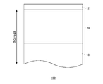
- FIG. 1 is a cross-sectional view showing an outline of a semiconductor device 100 according to an embodiment of the present invention.
- FIG. 17 is a diagram showing an example of the step of implanting the impurity into the impurity implanted region 20 in the manufacturing process of the semiconductor device 100;
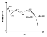
- FIG. 6 is a view showing an example of the impurity concentration distribution in the depth direction of the impurity implantation region 20.
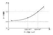
- FIG. 6 is a diagram showing the relationship between the total dose of impurities to the impurity implanted region 20 and the sheet resistance of the impurity implanted region 20. It is a figure which shows the impurity concentration distribution in an Example and a comparative example.
- FIG. 17 is a diagram showing an example of the step of implanting the impurity into the impurity implantation region in the manufacturing process of the semiconductor device according to the comparative example; It is a figure which compares the manufacturing efficiency in the impurity implantation process of a comparative example and an Example.
- FIG. 1 is a cross-sectional view showing an outline of a semiconductor device 100 according to an embodiment of the present invention.
- the semiconductor device 100 includes the SiC semiconductor layer 10.
- the SiC semiconductor layer 10 may be at least a part of a SiC substrate, or may be a semiconductor layer formed on the substrate by an epitaxial method or the like.
- the semiconductor device 100 functions as a diode, a transistor or another semiconductor element.
- the semiconductor device 100 of this example is a Schottky barrier diode, and includes the SiC semiconductor layer 10 and the electrode 12.
- the semiconductor device 100 is an IEMOS (Implementation and Epitaxial Metal Oxide Semiconductor) formed by epitaxially growing a SiC layer above the impurity-implanted SiC layer.
- IEMOS examplementation and Epitaxial Metal Oxide Semiconductor
- the semiconductor device 100 is not limited to these examples. In FIG. 1, only the vicinity of the top surface of the semiconductor device 100 is shown, and the other parts are omitted.
- the SiC semiconductor layer 10 of this example is a SiC substrate.
- the SiC semiconductor layer 10 has an impurity implanted region 20 into which an impurity is implanted.
- the impurity implanted region 20 functions as a predetermined impurity region in the semiconductor device 100.
- the impurity implanted region 20 may function as an n-type region or may function as a p-type region.
- An impurity according to the conductivity type is implanted into the impurity implanted region 20.
- the impurity implanted region 20 may function as an emitter region, a collector region, a source region or a drain region of a transistor, may function as a base region (channel region) of a MOS transistor, and may be an anode region of a diode. Alternatively, it may function as a cathode region.
- the impurity implanted region 20 functions as an anode region or a cathode region of the diode.
- the impurity implanted region 20 of this example is formed in a region in contact with the electrode 12.
- the electrode 12 of this example is a Schottky electrode which is formed on the upper surface of the SiC semiconductor layer 10 and which forms a Schottky junction with the impurity implanted region 20.
- the electrode 12 is formed of platinum (Pt).
- the direction perpendicular to the upper surface of the SiC semiconductor layer 10 on which the electrode 12 is formed is referred to as the depth direction.
- FIG. 2 is a view showing an example of the step of implanting the impurity into the impurity implanted region 20 in the manufacturing process of the semiconductor device 100.
- the step of implanting the impurity of this example is performed before forming the electrode 12.
- a mask patterned in a shape corresponding to the impurity implantation region 20 is formed on the upper surface of the SiC semiconductor layer 10.
- the mask layer is patterned by steps such as exposure and development.
- the mask in this example is a resist mask.
- the impurity is implanted into the impurity implanted region 20 of the SiC semiconductor layer 10 a plurality of times at different depths, with the temperature of the SiC semiconductor layer 10 kept at 150 ° C. or less.
- an impurity is implanted into the impurity implantation region 20 with the upper surface of the SiC semiconductor layer 10 as an implantation surface.
- the temperature of the SiC semiconductor layer 10 in the impurity implantation step S202 since the temperature of the SiC semiconductor layer 10 is set to 150 ° C. or less, the temperature rising and temperature lowering time of the SiC semiconductor layer 10 can be shortened. Therefore, the production efficiency of the semiconductor device 100 can be improved.
- the temperature of the SiC semiconductor layer 10 in the impurity implantation step S202 may be 120 ° C. or less, or may be 100 ° C. or less.
- the temperature of the SiC semiconductor layer 10 in the impurity implantation step S202 may be room temperature or higher.
- the room temperature is the temperature of the space in which the ion implantation apparatus is disposed, and is, for example, a temperature of about 20 ° C. or more and about 30 ° C. or less.
- the impurity is implanted into the impurity implantation region 20 a plurality of times at different depths, with the SiC semiconductor layer 10 placed in a room temperature atmosphere.
- an impurity may be implanted to each depth in order from the deep side, and an impurity may be implanted to each depth in order from the shallow side.
- the temperature of the SiC semiconductor layer 10 can be raised by implanting impurities into the SiC semiconductor layer 10. Even if the temperature of the SiC semiconductor layer 10 rises due to the impurity implantation, the temperature of the SiC semiconductor layer 10 may be controlled so that the temperature of the SiC semiconductor layer 10 becomes 150 ° C. or less. Thereby, the temperature rising and temperature lowering time of the SiC semiconductor layer 10 can be shortened.
- the temperature of the SiC semiconductor layer 10 in the impurity implantation step S202 is set to 150 ° C. or less. Therefore, a resist having relatively low heat resistance can be used as a mask formed on the upper surface of SiC semiconductor layer 10.
- a mask having high heat resistance such as an oxide film.
- the number of steps of the mask formation step S200 is increased. For example, after an oxide film is formed, a resist is patterned on the oxide film, the oxide film is etched, and the resist is peeled off, the impurity must be implanted.
- the manufacturing efficiency of the semiconductor device 100 is further improved.
- the resist mask is peeled.
- the resist mask may be peeled by ashing.
- the impurity implantation step S202 it is preferable to suppress the generation of crystal defects at the time of impurity implantation by controlling the total dose amount of the impurity and the like. Thereby, even if an impurity is implanted into SiC semiconductor layer 10 at a temperature of 150 ° C. or less, the increase in crystal defects in SiC semiconductor layer 10 can be alleviated.
- FIG. 3 is a view showing an example of the impurity concentration distribution in the depth direction of the impurity implantation region 20.
- the depth viewed from the impurity implantation surface of the SiC semiconductor layer 10 is taken as the horizontal axis, and the logarithmic impurity concentration is taken as the vertical axis.
- impurity ions are implanted three times into the impurity implanted region 20 while changing the depth.
- the impurity concentration distribution in the impurity implantation region 20 can be approximated by a Gaussian distribution with the concentration at the set implantation depth as the top.
- three Gaussian distributions overlap, and three peaks 22 and two valleys 24 are formed in the impurity concentration distribution.
- the peak is a point at which the impurity concentration shows a maximum value
- the valley is a point at which the impurity concentration shows a minimum value between two peaks.
- the first peak 22-1, the second peak 22-2, and the third peak 22-3 are in order from the deepest peak 22 as viewed from the impurity implantation surface toward the implantation surface. Further, from the deepest valley 24 viewed from the impurity implantation surface, the first valley 24-1 and the second valley 24-2 are sequentially formed toward the implantation surface.
- the impurity-implanted region 20 functions as an impurity region such as an emitter region
- the impurity is generally implanted such that the impurity concentration distribution in the depth direction is as uniform as possible.
- a uniform impurity concentration distribution is formed by implanting the impurity many times at short intervals in the depth direction.
- crystal defects will increase.
- the uniformity of the impurity concentration distribution in the impurity implantation region 20 is relaxed under the condition that the predetermined electrical characteristics are satisfied. That is, with respect to the impurity concentration of the peak 22, the impurity concentration of the valley 24 is lowered within a certain range. As a result, the total dose or the number of times of impurity implantation is reduced, and the increase in crystal defects is suppressed even if the impurity is implanted at a low temperature.
- the impurity is implanted so that the impurity concentration of the impurity implanted region 20 is 1.0 ⁇ 10 16 / cm 3 or more and 5.0 ⁇ 10 19 / cm 3 or less.
- the impurity concentration of the impurity implantation region 20 is the impurity concentrations P1 to P3 at the respective peaks 22 and the impurity concentrations V1 to V2 at the valleys 24. That is, it is preferable that the impurity concentration in all the peaks 22 and valleys 24 is in the above-mentioned range.
- the impurity-implanted region 20 does not have predetermined electrical characteristics. In addition, if the impurity concentration is too high, the total dose increases and crystal defects increase. In another example, the impurity may be implanted such that the impurity concentration of the impurity implanted region 20 is 1.0 ⁇ 10 18 / cm 3 or less. Thereby, the total dose can be further reduced.
- the ratio of the impurity concentration V1 of the first valley 24-1 to the impurity concentration P1 of the first peak 22-1 is preferably 10% or more and 60% or less.
- the first peak 22-1 is the deepest peak 22 among the plurality of peaks 22 as viewed from the impurity injection surface.
- the first valley 24-1 is the deepest valley 24 of the plurality of valleys 24 when viewed from the impurity implantation surface. If the ratio of the impurity concentration V1 of the first valley 24-1 is too low, the bias of the impurity distribution in the impurity implantation region 20 becomes large, and the bias of the electric field distribution becomes large.
- the impurity implanted region 20 As a result, in the impurity implanted region 20, a portion where current or charge tends to concentrate and a portion where concentration is difficult to occur may occur, and the breakdown voltage of the semiconductor device 100 may be reduced. If the ratio of the impurity concentration V1 in the first valley 24-1 is too high, the total dose or the number of times of impurity implantation can not be reduced, and crystal defects increase.
- the lower limit of the ratio of the impurity concentration V1 of the first valley 24-1 to P1 may be 20% or 30%. Further, the upper limit of the ratio of the impurity concentration V1 of the first valley 24-1 to P1 may be 50% or 40%.
- the impurity concentration of the other valleys 24 is also preferably 10% or more and 60% or less with respect to the impurity concentration of the peak 22 adjacent to the deep side.
- the lower limit of the ratio may be 20% or 30%.
- the upper limit of the ratio may be 50% or 40%.
- the distance between the peaks 22 in the impurity implanted region 20 in the depth direction can be obtained by the following equation (1).
- the distance between adjacent peaks 22 is d p
- the ratio of the impurity concentration of the valley 24 to the impurity concentration of the peak 22 adjacent to the deep side in the valley 24 between the adjacent peaks 22 is a
- the impurity concentration distribution of the adjacent peaks 22 Let their standard deviations be ⁇ 1 (the deep side in the depth direction) and ⁇ 2 (the shallow side in the depth direction).
- the standard deviation of the impurity concentration is determined by the ion species and the acceleration voltage.
- the depth positions of the first peak 22-1, the second peak 22-2, and the third peak 22-3 are D1, D2, and D3, respectively. Between D1 and D2 and between D2 and D3 correspond to intervals D1-D2 and intervals D2-D3 of the peaks 22 respectively.
- the d p in the above equation (1) corresponds to the interval D1-D2 and the interval D2-D3. If the distance d p of the above formula (1) and the spacing D1-D2, the ratio a represents a ratio of the impurity concentration V1 of the first trough 24-1 with respect to the impurity concentration P1 of the first peak 22-1.
- the standard deviation sigma 1 represents the standard deviation of the distribution of impurity concentration peaks 22-1, standard deviation sigma 2 shows the standard deviation of the impurity concentration distribution of the peak 22-2.
- the ratio a of the impurity concentration V of the valley 24 between adjacent peaks to the impurity concentration P of the peak 22 on the deep side in the depth direction of the adjacent peaks 22 is the following equation (2 ).
- 10% ratio a of the impurity concentration V of valley 24 between peaks 22 adjacent to the impurity concentration P of the depth direction deeper side of the peak 22 of the adjacent peak 22 or more, preferably 60% or less, distance d p is the following Equation (3) of
- FIG. 3 shows an example in which the ion species is Al.
- the acceleration voltage of the first peak 22-1 is 150 eV
- ⁇ 1 is 0.04938
- ⁇ 2 is 0.01388.
- the ratio a of the impurity concentration V of the valley 24 between adjacent peaks to the impurity concentration P of the peak 22 on the deep side in the depth direction of the adjacent peaks 22 is 10% or more
- the distance d p (the distance D 1 -D 2) in the impurity implantation region 20 is 0.06 ⁇ m or more and 0.13 ⁇ m or less.
- the acceleration voltage of the first peak 22-1 is 350 eV
- ⁇ 1 is 0.08422
- ⁇ 2 is 0.04938
- the ratio a of the impurity concentration V of the valley 24 between adjacent peaks to the impurity concentration P of the peak 22 on the deep side in the depth direction of the adjacent peaks 22 is 10% or more
- the distance d p (the distance D 1 -D 2) in the impurity implantation region 20 is 0.13 ⁇ m or more and 0.28 ⁇ m or less.
- examples of the first peak 22-1 and the second peak 22-2 are shown, but the above-mentioned formulas (1), (2) and It can be set by (3).
- the interval of each peak 22 in the range satisfying the above equation (3), it is possible to suppress the occurrence of a portion where current or charge is likely to be concentrated and a portion where it is difficult to concentrate in the impurity implanted region 20.
- the number can be reduced.
- the number of peaks 22 and valleys 24 may be varied according to the depth of the impurity implanted region 20 to be formed.
- the distance between the peaks 22 in the impurity concentration distribution in the depth direction may be wider as the impurity implantation surface is deeper.
- the interval D1-D2 between the first peak 22-1 and the second peak 22-2 is larger than the interval D2-D3 between the second peak 22-2 and the third peak 22-3.
- the range of the impurity increases as the deep peak 22 is seen from the impurity implantation surface, and the variation in the depth to which the impurity is implanted increases.
- the deeper peak 22 has an impurity concentration distribution that approximates to a gentle Gaussian distribution. Therefore, in the relatively deep peak 22, even if the distance between the peaks 22 is increased, the impurity concentration of the adjacent valley 24 can be maintained, and the uniformity of the impurity concentration distribution can be easily maintained. That is, by increasing the distance between the deep peaks 22, the number of impurity implantation stages can be reduced while maintaining the uniformity of the impurity concentration distribution.
- the depths of the first peak 22-1, the second peak 22-2, and the third peak 22-3 may be 1.0 ⁇ m or less as viewed from the impurity injection surface.
- the depth of the first peak 22-1 may be 0.2 ⁇ m or more and 1.0 ⁇ m or less as viewed from the impurity implantation surface.
- the depth of the first peak 22-1 may be 0.3 ⁇ m or more and 0.5 ⁇ m or less.
- the depth of the second peak 22-2 may be 0.1 ⁇ m or more and 0.3 ⁇ m or less.
- the depth of the third peak 22-3 may be 0 ⁇ m or more and 0.1 ⁇ m or less.
- the impurity concentration P1 of the deepest first peak 22-1 as viewed from the impurity implantation surface may be higher than the impurity concentration P2 of the second deep second peak 22-2.
- the impurity concentration of the deepest peak 22 high, it can be suppressed that the impurity concentration of the peak 22 is smaller than the impurity concentration of the other peaks 22. Therefore, the uniformity of the impurity concentration distribution can be easily maintained.
- FIG. 4 is a view showing the relationship between the total dose amount of the impurity to the impurity implanted region 20 and the sheet resistance of the impurity implanted region 20.
- the vertical axis in FIG. 4 corresponds to the maximum value of the symmetry factor of Hall measurement. If the said maximum value is 1.5 or less, it will become sheet resistance suitable as a semiconductor element.
- the minimum value of the vertical axis in FIG. Moreover, in this example, aluminum ion was used as an impurity. However, other impurities such as nitrogen, phosphorus, arsenic and boron are also the same.
- the SiC semiconductor layer 10 was placed in a room temperature atmosphere and an impurity was implanted.
- the total dose of the impurity to the impurity-implanted region 20 is 6.0 ⁇ 10 14 / cm 2 .
- the total dose of impurities into the impurity implantation region 20 may be 1.55 ⁇ 10 14 / cm 2 .
- the number of crystal defects hardly increases, or the number of crystal defects is very small as compared with the case where the total dose amount is 6.0 ⁇ 10 14 / cm 2 .
- the lower limit of the total dose may be 1.0 ⁇ 10 11 / cm 2 , 1.0 ⁇ 10 12 / cm 2 or 1.0 ⁇ 10 13 / cm 2. Good.
- FIG. 5 is a view showing the impurity concentration distribution in the example and the comparative example.
- the vertical axis in FIG. 5 is a logarithmic axis.
- the SiC semiconductor layer 10 was placed in a room temperature atmosphere, and aluminum ions were implanted to three levels of depth.
- aluminum ions were implanted to a depth of five steps.
- the total dose amount was 1.7 ⁇ 10 13 / cm 2 .
- the example shows a higher impurity concentration than the comparative example.
- the example shows a smaller impurity concentration than the comparative example.
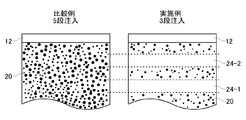
- FIG. 6 is a schematic view showing crystal defects in the impurity implanted regions 20 of the example and the comparative example. Black circles in the impurity implanted region 20 indicate crystal defects.
- FIG. 6 a transmission electron micrograph of a cross section of the impurity implantation region 20 is schematically shown. As shown in FIG. 6, in the embodiment in which the impurity is implanted in three stages in a room temperature atmosphere, the generation of crystal defects in the region of the valley 24 is suppressed. In addition, in the region other than the valleys 24, there are relatively few crystal defects. As shown in FIG. 6, even if the total dose of impurities is the same, the occurrence of crystal defects can be suppressed by reducing the number of impurity implantation stages.
- FIG. 7 is a view showing an example of the step of implanting the impurity into the impurity implantation region in the manufacturing process of the semiconductor device according to the comparative example.
- the SiC semiconductor layer is heated to about 500 ° C. and the impurities are implanted, a mask having high heat resistance must be formed.
- the mask oxidation step S702 the upper surface of the SiC semiconductor layer is oxidized to form an oxide film.
- a resist is formed on the oxide film, and the resist is patterned by exposure, development, and the like.
- the oxide film is etched using the resist as a mask.
- the peeling step S708 the resist on the oxide film is removed.
- impurities are implanted into the SiC semiconductor layer using the oxide film as a mask. After the impurity is implanted, the temperature of the SiC semiconductor layer is lowered to room temperature. Next, in a mask removal step S712, the oxide film mask is removed.
- the impurity is implanted at a high temperature, it takes time to raise and lower the temperature. Further, since an oxide film or the like having high heat resistance is used as a mask, the process of patterning the mask also takes time.
- FIG. 8 is a diagram for comparing the manufacturing efficiency in the impurity implantation step of the comparative example and the example.
- the vertical axis in FIG. 8 indicates the number of semiconductor devices that can carry out the impurity implantation step in a unit period when using the same device.
- the semiconductor device 100 according to the embodiment can perform the impurity implantation process at about twice the efficiency of the semiconductor device according to the comparative example.
Landscapes
- Electrodes Of Semiconductors (AREA)
- Crystals, And After-Treatments Of Crystals (AREA)
- Insulated Gate Type Field-Effect Transistor (AREA)
Abstract
炭化珪素半導体層に不純物を注入する工程を効率化する。炭化珪素半導体層を備える半導体装置の製造方法であって、炭化珪素半導体層の温度を150℃以下とした状態で、炭化珪素半導体層における不純物注入領域に対して異なる深さに複数回不純物を注入する不純物注入段階を備える製造方法を提供する。不純物注入段階において、炭化珪素半導体層の温度を室温以上とした状態で、不純物注入領域に対して異なる深さに複数回不純物を注入してよい。
Description
本発明は、半導体装置の製造方法および半導体装置に関する。
従来、炭化珪素(本明細書では、SiCと称する場合がある)を用いた半導体装置が知られている。SiC基板にデバイス構造を形成するための不純物注入プロセスとして、イオン注入法が知られている(例えば、特許文献1参照)。
特許文献1 特開2009-252811号公報
特許文献1 特開2009-252811号公報
イオン注入時の結晶欠陥発生を抑制すべく、イオン注入時の基板温度は175℃~500℃程度に設定される。基板温度を高温にすることで結晶欠陥の発生は抑制できるが、基板の昇温および降温に時間がかかってしまう。
本発明の第1の態様においては、炭化珪素半導体層を備える半導体装置の製造方法を提供する。製造方法は、炭化珪素半導体層の温度を150℃以下とした状態で、炭化珪素半導体層における不純物注入領域に不純物を注入する不純物注入段階を備えてよい。不純物注入段階において、不純物注入領域に対して異なる深さに複数回不純物を注入してよい。
不純物注入段階において、炭化珪素半導体層の温度を室温以上とした状態で、不純物注入領域に対して異なる深さに複数回不純物を注入してよい。不純物注入段階において、炭化珪素半導体層を室温雰囲気に配置した状態で、不純物注入領域に対して異なる深さに複数回不純物を注入してよい。
不純物注入段階において、不純物注入領域の不純物濃度が、1.0×10¹⁶/cm3以上、5.0×1019/cm3以下となるように不純物を注入してよい。不純物注入段階において、不純物注入領域の不純物濃度が、1.0×1018/cm3以下となるように不純物を注入してよい。
不純物注入段階において不純物が注入された不純物注入領域の深さ方向における不純物濃度分布は、複数のピークおよび複数の谷を有してよい。ピークのうち、炭化珪素半導体層の不純物が注入される注入面からみて最も深い第1ピークの不純物濃度に対して、谷のうち、注入面からみて最も深い第1谷の不純物濃度の割合が、10%以上、60%以下であってよい。
不純物濃度分布におけるそれぞれのピークの、深さ方向における間隔dpが下記式(3)を満たしてよい。

ただし、隣り合う複数のピークの深さ方向に深い側のピークの不純物濃度分布の標準偏差はσ1、深さ方向に浅い側のピークの不純物濃度分布の標準偏差はσ2である。
炭化珪素半導体層の不純物が注入される注入面からみて深いほど、不純物濃度分布におけるそれぞれのピークの深さ方向における間隔が広くてよい。炭化珪素半導体層の不純物が注入される注入面からみて最も深いピークの不純物濃度は、2番目に深いピークの不純物濃度よりも高くてよい。
不純物注入段階における総ドーズ量が6.0×10¹⁴/cm2以下であってよい。不純物注入段階における総ドーズ量が1.55×1014/cm2以下であってよい。ピークのうち、炭化珪素半導体層の不純物が注入される注入面からみて最も深い第1ピークの深さが、0.2μm以上、1.0μm以下であってよい。不純物注入段階の前に、炭化珪素半導体層の上方に不純物注入領域に応じた形状のレジストマスクを形成するマスク形成段階を備えてよい。
本発明の第2の態様においては、炭化珪素半導体層を備える半導体装置を提供する。炭化珪素半導体層は、不純物が注入された不純物注入領域を有してよい。不純物注入領域の深さ方向における不純物濃度分布は、複数のピークおよび複数の谷を有してよい。炭化珪素半導体層の不純物が注入される注入面からみて深いほど、不純物濃度分布におけるそれぞれのピークの深さ方向における間隔が広くてよい。
不純物注入領域の深さ方向の不純物濃度分布において、炭化珪素半導体層の不純物が注入される注入面からみて最も深いピークの不純物濃度は、2番目に深いピークの不純物濃度よりも高くてよい。
上記の発明の概要は、本発明の特徴の全てを列挙したものではない。これらの特徴群のサブコンビネーションも発明となりうる。
以下、発明の実施の形態を通じて本発明を説明するが、以下の実施形態は請求の範囲にかかる発明を限定するものではない。また、実施形態の中で説明されている特徴の組み合わせの全てが発明の解決手段に必須であるとは限らない。
図1は、本発明の一つの実施形態に係る半導体装置100の概要を示す断面図である。半導体装置100は、SiC半導体層10を備える。SiC半導体層10は、SiC基板の少なくとも一部であってよく、エピタキシャル法等によって基板上に形成された半導体層であってもよい。
半導体装置100は、ダイオード、トランジスタまたはその他の半導体素子として機能する。本例の半導体装置100は、ショットキーバリアダイオードであり、SiC半導体層10および電極12を備える。他の例では、半導体装置100は、不純物を注入したSiC層の上方にSiC層をエピタキシャル成長させて形成したIEMOS(Implantation and Epitaxial Metal Oxide Semiconductor)である。ただし半導体装置100はこれらの例に限定されない。なお図1においては、半導体装置100の上面近傍だけを示しており、他の部分を省略している。
本例のSiC半導体層10は、SiC基板である。SiC半導体層10は、不純物が注入される不純物注入領域20を有する。不純物注入領域20は、半導体装置100における所定の不純物領域として機能する。例えば不純物注入領域20は、n型領域として機能してよく、p型領域として機能してもよい。不純物注入領域20には、導電型に応じた不純物が注入される。より具体的には、不純物注入領域20は、トランジスタのエミッタ領域、コレクタ領域、ソース領域またはドレイン領域として機能してよく、MOSトランジスタのベース領域(チャネル領域)として機能してよく、ダイオードのアノード領域またはカソード領域として機能してもよい。
本例において不純物注入領域20は、ダイオードのアノード領域またはカソード領域として機能する。本例の不純物注入領域20は、電極12と接触する領域に形成される。本例の電極12は、SiC半導体層10の上面に形成され、不純物注入領域20とショットキー接合を形成するショットキー電極である。一例として電極12は白金(Pt)で形成される。なお、SiC半導体層10において電極12が形成される上面と垂直な方向を、深さ方向と称する。
図2は、半導体装置100の製造工程のうち、不純物注入領域20に不純物を注入する工程の一例を示す図である。本例の不純物を注入する工程は、電極12を形成する前に行う。まず、マスク形成段階S200において、SiC半導体層10の上面に、不純物注入領域20に応じた形状にパターニングされたマスクを形成する。本例のマスク形成段階S200においては、SiC半導体層10の上面全体にマスク層を形成した後に、露光および現像等の工程によりマスク層をパターニングする。本例におけるマスクはレジストマスクである。
次に、不純物注入段階S202において、SiC半導体層10の温度を150℃以下とした状態で、SiC半導体層10の不純物注入領域20に対して異なる深さに複数回不純物を注入する。不純物注入段階S202では、SiC半導体層10の上面を注入面として、不純物注入領域20に不純物を注入する。
不純物注入段階S202においては、SiC半導体層10の温度を150℃以下としているので、SiC半導体層10の昇温および降温時間を短くすることができる。このため、半導体装置100の生産効率を向上させることができる。不純物注入段階S202におけるSiC半導体層10の温度は、120℃以下であってよく、100℃以下であってもよい。
不純物注入段階S202におけるSiC半導体層10の温度は、室温以上としてよい。室温とは、イオン注入装置が配置された空間の温度であり、例えば20℃以上、30℃以下程度の温度である。
本例の不純物注入段階S202では、SiC半導体層10を室温雰囲気に配置した状態で、不純物注入領域20に対して異なる深さに複数回不純物を注入する。不純物注入段階S202では、深い側から順番に、それぞれの深さに不純物を注入してよく、浅い側から順番に、それぞれの深さに不純物を注入してもよい。
なお、SiC半導体層10に不純物を注入することでSiC半導体層10の温度は上昇し得る。不純物注入によりSiC半導体層10の温度が上昇しても、SiC半導体層10の温度は150℃以下となるように、SiC半導体層10の温度を制御してよい。これにより、SiC半導体層10の昇温および降温時間を短くできる。
なお、不純物注入段階S202におけるSiC半導体層10の温度を150℃以下としている。このためSiC半導体層10の上面に形成するマスクとして、比較的に耐熱性の低いレジストを用いることができる。高温状態でSiC半導体層10に不純物を注入する場合、酸化膜等の耐熱性の高いマスクを用いなければならない。しかし、酸化膜等をマスクとして用いると、マスク形成段階S200の工程数が増大してしまう。例えば、酸化膜を形成し、酸化膜上にレジストをパターニングし、酸化膜をエッチングし、レジストを剥離してから、不純物を注入しなければならない。
これに対して本例では、不純物注入用のマスクとしてレジストマスクを用いることができるので、マスク形成段階S200の工程数を削減できる。このため、半導体装置100の製造効率が更に向上する。
次に、剥離段階S204において、レジストマスクを剥離する。剥離段階S204においては、アッシングによりレジストマスクを剥離してよい。
なお、不純物注入段階S202においては、不純物の総ドーズ量等を制御することで、不純物注入時における結晶欠陥の発生を抑制することが好ましい。これにより、150℃以下の温度でSiC半導体層10に不純物を注入しても、SiC半導体層10における結晶欠陥の増加を緩和することができる。
図3は、不純物注入領域20の深さ方向における不純物濃度分布の一例を示す図である。図3では、SiC半導体層10の不純物注入面からみた深さを横軸とし、対数の不純物濃度を縦軸としている。本例では、不純物注入領域20に対して、深さを変えて3回不純物イオンを注入している。
不純物注入領域20における不純物濃度分布は、設定される注入深さでの濃度を頂点としたガウス分布で近似できる。本例では深さを変えて3回不純物イオンを注入しているので、3つのガウス分布が重なり合い、不純物濃度分布には、3つのピーク22と、2つの谷24とが形成される。ピークは、不純物濃度が極大値を示す点であり、谷は、2つのピークの間において不純物濃度が極小値を示す点である。
図3においては、不純物注入面からみて最も深いピーク22から、注入面に向かって順番に、第1ピーク22-1、第2ピーク22-2、第3ピーク22-3とする。また、不純物注入面からみて最も深い谷24から、注入面に向かって順番に、第1谷24-1、第2谷24-2とする。
不純物注入領域20がエミッタ領域等の不純物領域として機能する場合、一般に深さ方向における不純物濃度分布ができるだけ均一となるように、不純物が注入される。例えば、深さ方向において短い間隔で多数回不純物を注入することで、均一な不純物濃度分布を形成する。しかし、不純物を多数回注入して均一な不純物濃度分布を形成しようとすると、結晶欠陥が増大してしまう。
本例では、所定の電気的特性を満たす条件で、不純物注入領域20における不純物濃度分布の均一性を緩和する。つまり、ピーク22の不純物濃度に対して、一定の範囲で谷24の不純物濃度を低下させる。これにより、総ドーズ量または不純物注入回数が低減され、低温で不純物を注入しても、結晶欠陥の増大が抑制される。
なお不純物注入領域20の不純物濃度が、1.0×10¹⁶/cm3以上、5.0×1019/cm3以下となるように不純物を注入することが好ましい。不純物注入領域20の不純物濃度は、それぞれのピーク22における不純物濃度P1~P3および谷24における不純物濃度V1~V2である。つまり、全てのピーク22および谷24における不純物濃度が、上述した範囲内であることが好ましい。
不純物濃度が低すぎると、不純物注入領域20が所定の電気的特性を有さなくなる。また、不純物濃度が高すぎると、総ドーズ量が増大して結晶欠陥が増大してしまう。他の例では、不純物注入領域20の不純物濃度が、1.0×10¹⁸/cm3以下となるように不純物を注入してもよい。これにより、総ドーズ量を更に低減することができる。
また、第1ピーク22-1の不純物濃度P1に対して、第1谷24-1の不純物濃度V1の割合は、10%以上、60%以下であることが望ましい。第1ピーク22-1は、複数のピーク22のうち不純物注入面からみて最も深いピーク22である。第1谷24-1は、複数の谷24のうち不純物注入面からみて最も深い谷24である。第1谷24-1の不純物濃度V1の割合が低すぎると、不純物注入領域20における不純物分布の偏りが大きくなり、電界分布の偏りが大きくなる。このため、不純物注入領域20内で、電流や電荷等が集中しやすい部分と集中しにくい部分が生じ、半導体装置100の耐圧が低下してしまう可能性がある。また、第1谷24-1の不純物濃度V1の割合が高すぎると、総ドーズ量または不純物注入回数を低減できずに結晶欠陥が増大してしまう。
第1谷24-1の不純物濃度V1のP1に対する割合の下限は、20%であってよく、30%であってもよい。また、第1谷24-1の不純物濃度V1のP1に対する割合の上限は、50%であってよく、40%であってもよい。
また、他の谷24の不純物濃度も、深い側に隣接するピーク22の不純物濃度に対して10%以上、60%以下であることが望ましい。当該割合の下限は、20%であってよく、30%であってもよい。当該割合の上限は、50%であってよく、40%であってもよい。
また、不純物注入領域20におけるそれぞれのピーク22の、深さ方向における間隔は下記の式(1)により求められる。

隣り合うピーク22間の距離をdp、隣り合うピーク22間にある谷24において深い側に隣接するピーク22の不純物濃度に対する谷24の不純物濃度の割合をa、隣り合うピーク22の不純物濃度分布のそれぞれの標準偏差をσ1(深さ方向において深い側)およびσ2(深さ方向において浅い側)とする。なお、不純物濃度の標準偏差はイオン種と加速電圧で決定される。
図3の例においては、第1ピーク22-1、第2ピーク22-2および第3ピーク22-3のそれぞれの深さ位置をD1、D2、D3とする。D1とD2との間、および、D2とD3との間が、各ピーク22の間隔D1-D2、および、間隔D2-D3に相当する。上記の式(1)のdpは、間隔D1-D2、および、間隔D2-D3に相当する。上記の式(1)の間隔dpを間隔D1-D2とした場合は、割合aは第1ピーク22-1の不純物濃度P1に対する第1谷24-1の不純物濃度V1の割合を示す。標準偏差σ1はピーク22-1の不純物濃度分布の標準偏差を示し、標準偏差σ2はピーク22-2の不純物濃度分布の標準偏差を示す。
また、上記の式(1)より、隣り合うピーク22の深さ方向に深い側のピーク22の不純物濃度Pに対する隣り合うピーク間の谷24の不純物濃度Vの割合aは、下記の式(2)となる。
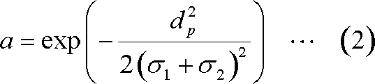
隣り合うピーク22の深さ方向に深い側のピーク22の不純物濃度Pに対する隣り合うピーク22間の谷24の不純物濃度Vの割合aは10%以上、60%以下が望ましく、間隔dpは下記の式(3)を満たす。

一例として、図3においてイオン種がAlである例を示す。第1ピーク22-1の加速電圧が150eVの場合はσ1が0.04938、第2ピーク22-2の加速電圧が30eVの場合はσ2が0.01388である。上記の式(2)、(3)より、隣り合うピーク22の深さ方向に深い側のピーク22の不純物濃度Pに対する隣り合うピーク間の谷24の不純物濃度Vの割合aが10%以上、60%以下とするには、不純物注入領域20における間隔dp(間隔D1-D2)は0.06μm以上、0.13μm以下となる。
また、第1ピーク22-1の加速電圧が350eVの場合はσ1が0.08422、第2ピーク22-2の加速電圧が150eVの場合はσ2が0.04938である。上記の式(2)、(3)より、隣り合うピーク22の深さ方向に深い側のピーク22の不純物濃度Pに対する隣り合うピーク間の谷24の不純物濃度Vの割合aが10%以上、60%以下とするには、不純物注入領域20における間隔dp(間隔D1-D2)は0.13μm以上、0.28μm以下となる。
本例では、第1ピーク22-1および第2ピーク22-2の例を示したが、他のピーク22と谷24の間隔についても、同様に上記の式(1)、(2)、および(3)によって設定できる。各ピーク22の間隔を上記の式(3)を満たす範囲とすることで、不純物注入領域20内に電流や電荷等が集中しやすい部分と集中しにくい部分が生じることを抑制し、ピーク22の数を減少させることができる。なお、ピーク22および谷24の数は形成する不純物注入領域20の深さによって変動させてもよい。
また、不純物注入面からみて深いほど、不純物濃度分布におけるそれぞれのピーク22の深さ方向における間隔が広くなっていてよい。本例では、第1ピーク22-1および第2ピーク22-2の間隔D1-D2が、第2ピーク22-2および第3ピーク22-3の間隔D2-D3よりも大きい。不純物注入面からみて深いピーク22ほど不純物の飛程が大きくなり、不純物が注入される深さのバラツキが増大する。
つまり、深いピーク22ほど、なだらかなガウス分布に近似した不純物濃度分布を有する。このため、比較的深いピーク22では、ピーク22の間隔を大きくしても、隣接する谷24の不純物濃度を維持することができ、不純物濃度分布の均一性を保ちやすい。つまり、深い位置のピーク22の間隔を大きくすることで、不純物濃度分布の均一性を保ちつつ、不純物注入の段数を低減することができる。
一例として、第1ピーク22-1、第2ピーク22-2、および第3ピーク22-3の深さは、不純物注入面からみて1.0μm以下であってよい。また、一例として、第1ピーク22-1の深さは、不純物注入面からみて0.2μm以上、1.0μm以下であってよい。第1ピーク22-1の深さは、0.3μm以上、0.5μm以下であってもよい。
第2ピーク22-2の深さは、0.1μm以上、0.3μm以下であってよい。第3ピーク22-3の深さは、0μm以上、0.1μm以下であってよい。
また、不純物注入面からみて最も深い第1ピーク22-1の不純物濃度P1は、2番目に深い第2ピーク22-2の不純物濃度P2よりも高くてよい。上述したように、深いピーク22ほど、不純物が注入される深さにバラツキが生じるので、ピーク22における不純物濃度は全体的に平均化され、極大値が低くなりやすい。これに対して、最も深いピーク22の不純物濃度を高く設定しておくことで、当該ピーク22の不純物濃度が、他のピーク22の不純物濃度に比べて小さくなることを抑制できる。このため、不純物濃度分布の均一性を保ちやすくなる。
図4は、不純物注入領域20への不純物の総ドーズ量と、不純物注入領域20のシート抵抗との関係を示す図である。図4の例では、ホール測定の結果から、半導体素子として好適なシート抵抗か否かを判定した。図4における縦軸は、ホール測定のシンメトリーファクターの最大値に対応する。当該最大値が1.5以下であれば、半導体素子として好適なシート抵抗となる。なお図4における縦軸の最小値は1である。また、本例では不純物としてアルミニウムイオンを用いた。ただし、窒素、リン、砒素、ボロン等の他の不純物も同様である。また、SiC半導体層10を室温雰囲気に載置して不純物を注入した。
図4に示すように、総ドーズ量が6.0×10¹⁴/cm2を超えると、シート抵抗が好適な値を超える。このため、不純物注入領域20への不純物の総ドーズ量は、6.0×1014/cm2であることが好ましい。不純物注入領域20への不純物の総ドーズ量は、1.55×1014/cm2であってもよい。この場合、結晶欠陥はほとんど増加しないか、または、総ドーズ量が6.0×1014/cm2の場合に比べて結晶欠陥が非常に少ない。なお、総ドーズ量の下限は、1.0×1011/cm2であってよく、1.0×1012/cm2であってよく、1.0×1013/cm2であってもよい。
図5は、実施例および比較例における不純物濃度分布を示す図である。図5における縦軸は対数軸である。実施例においては、SiC半導体層10を室温雰囲気に配置して、3段階の深さにアルミニウムイオンを注入した。比較例においては、SiC半導体層10を500℃に加熱した状態で、5段階の深さにアルミニウムイオンを注入した。実施例および比較例のそれぞれにおいて、総ドーズ量は1.7×10¹³/cm2とした。
図5に示すように、実施例の各ピーク22の位置においては、実施例は比較例より高い不純物濃度を示している。一方で、谷24の位置においては、実施例は比較例に対して小さい不純物濃度を示している。
図6は、実施例および比較例の不純物注入領域20における結晶欠陥を示す模式図である。不純物注入領域20における黒丸が、結晶欠陥を示している。図6では、不純物注入領域20の断面の透過型電子顕微鏡写真を、模式的に示している。図6に示すように、室温雰囲気で不純物を3段注入した実施例では、谷24の領域における結晶欠陥の発生が抑制されている。また、谷24以外の領域でも、結晶欠陥が比較的に少ない。図6に示すように、不純物の総ドーズ量が同一であっても、不純物の注入段数を減らすことで、結晶欠陥の発生を抑制できる。
図7は、比較例に係る半導体装置の製造工程のうち、不純物注入領域に不純物を注入する工程の一例を示す図である。比較例においては、SiC半導体層を500℃程度に加熱して不純物を注入するので、耐熱性の高いマスクを形成しなければならない。まず、マスク酸化段階S702において、SiC半導体層の上面を酸化して、酸化膜を形成する。
次に、パターニング段階S704において、酸化膜上にレジストを形成して、露光および現像等によりレジストをパターニングする。次に、エッチング段階S706において、レジストをマスクとして酸化膜をエッチングする。次に剥離段階S708において、酸化膜上のレジストを除去する。
次に、不純物注入段階S710において、SiC半導体層を500℃程度に加熱した状態で、酸化膜をマスクとして、SiC半導体層に不純物を注入する。不純物を注入した後、SiC半導体層を室温まで降温する。次に、マスク除去段階S712において、酸化膜マスクを除去する。
このように、比較例に係る半導体装置においては、高温で不純物を注入するので、昇温および降温に時間がかかってしまう。また、耐熱性の高い酸化膜等をマスクとして用いるので、マスクをパターニングする工程も時間がかかってしまう。
これに対して図2に示した半導体装置100の製造工程においては、SiC半導体層10を昇温および降温する時間が無いか、または、非常に短い。また、耐熱性の低いレジストをマスクとして用いることができるので、マスクをパターニングする工程も短時間でできる。このため、半導体装置100の製造効率を向上させることができる。
図8は、比較例および実施例の不純物注入工程における製造効率を比較する図である。図8の縦軸は、同等の装置を用いた場合における、単位期間内に不純物注入工程を実施可能な半導体装置の数量を示している。図8に示すように、実施例に係る半導体装置100は、比較例に係る半導体装置に比べて、倍程度の効率で不純物注入工程を実施できる。
以上、本発明を実施の形態を用いて説明したが、本発明の技術的範囲は上記実施の形態に記載の範囲には限定されない。上記実施の形態に、多様な変更または改良を加えることが可能であることが当業者に明らかである。その様な変更または改良を加えた形態も本発明の技術的範囲に含まれ得ることが、請求の範囲の記載から明らかである。
請求の範囲、明細書、および図面中において示した方法における動作、手順、ステップ、および段階等の各処理の実行順序は、特段「より前に」、「先立って」等と明示しておらず、また、前の処理の出力を後の処理で用いるのでない限り、任意の順序で実現しうることに留意すべきである。請求の範囲、明細書、および図面中の動作フローに関して、便宜上「まず、」、「次に、」等を用いて説明したとしても、この順で実施することが必須であることを意味するものではない。
10・・・SiC半導体層、12・・・電極、20・・・不純物注入領域、22・・・ピーク、24・・・谷、100・・・半導体装置
Claims (15)
- 炭化珪素半導体層を備える半導体装置の製造方法であって、
前記炭化珪素半導体層の温度を150℃以下とした状態で、前記炭化珪素半導体層における不純物注入領域に対して異なる深さに複数回不純物を注入する不純物注入段階を備える製造方法。 - 前記不純物注入段階において、前記炭化珪素半導体層の温度を室温以上とした状態で、前記不純物注入領域に対して異なる深さに複数回不純物を注入する
請求項1に記載の製造方法。 - 前記不純物注入段階において、前記炭化珪素半導体層を室温雰囲気に配置した状態で、前記不純物注入領域に対して異なる深さに複数回不純物を注入する
請求項2に記載の製造方法。 - 前記不純物注入段階において、前記不純物注入領域の不純物濃度が、1.0×10¹⁶/cm3以上、5.0×1019/cm3以下となるように不純物を注入する
請求項1から3のいずれか一項に記載の製造方法。 - 前記不純物注入段階において、前記不純物注入領域の不純物濃度が、1.0×10¹⁸/cm3以下となるように不純物を注入する
請求項4に記載の製造方法。 - 前記不純物注入段階において前記不純物が注入された前記不純物注入領域の深さ方向における不純物濃度分布は、複数のピークおよび複数の谷を有し、
前記複数のピークのうち、前記炭化珪素半導体層の前記不純物が注入される注入面からみて最も深い第1ピークの不純物濃度に対して、前記複数の谷のうち、前記注入面からみて最も深い第1谷の不純物濃度の割合が、10%以上、60%以下である
請求項4または5に記載の製造方法。 - 前記不純物注入段階において前記不純物が注入された前記不純物注入領域の深さ方向における不純物濃度分布は、複数のピークおよび複数の谷を有し、
前記不純物濃度分布におけるそれぞれのピークの、深さ方向における間隔dpが下記式(3)を満たす
請求項6に記載の製造方法。

- 前記不純物注入段階において前記不純物が注入された前記不純物注入領域の深さ方向における不純物濃度分布は、複数のピークおよび複数の谷を有し、
前記炭化珪素半導体層の前記不純物が注入される注入面からみて深いほど、前記不純物濃度分布におけるそれぞれのピークの深さ方向における間隔が広い
請求項1から7のいずれか一項に記載の製造方法。 - 前記不純物注入段階において前記不純物が注入された前記不純物注入領域の深さ方向における不純物濃度分布は、複数のピークおよび複数の谷を有し、
前記炭化珪素半導体層の前記不純物が注入される注入面からみて最も深いピークの不純物濃度は、2番目に深いピークの不純物濃度よりも高い
請求項1から8のいずれか一項に記載の製造方法。 - 前記不純物注入段階における総ドーズ量が6.0×10¹⁴/cm2以下である
請求項1から9のいずれか一項に記載の製造方法。 - 前記不純物注入段階における総ドーズ量が1.55×10¹⁴/cm2以下である
請求項10に記載の製造方法。 - 前記不純物注入段階において前記不純物が注入された前記不純物注入領域の深さ方向における不純物濃度分布は、複数のピークおよび複数の谷を有し、
前記複数のピークのうち、前記炭化珪素半導体層の前記不純物が注入される注入面からみて最も深い第1ピークの深さが、0.2μm以上、1.0μm以下である
請求項1から11のいずれか一項に記載の製造方法。 - 前記不純物注入段階の前に、前記炭化珪素半導体層の上方に前記不純物注入領域に応じた形状のレジストマスクを形成するマスク形成段階を備える
請求項1から12のいずれか一項に記載の製造方法。 - 炭化珪素半導体層を備える半導体装置であって、
前記炭化珪素半導体層は、不純物が注入された不純物注入領域を有し、
前記不純物注入領域の深さ方向における不純物濃度分布は、複数のピークおよび複数の谷を有し、
前記炭化珪素半導体層の前記不純物が注入される注入面からみて深いほど、前記不純物濃度分布におけるそれぞれのピークの深さ方向における間隔が広い半導体装置。 - 前記不純物注入領域の深さ方向の不純物濃度分布において、前記炭化珪素半導体層の前記不純物が注入される注入面からみて最も深いピークの不純物濃度は、2番目に深いピークの不純物濃度よりも高い
請求項14に記載の半導体装置。
Priority Applications (4)
| Application Number | Priority Date | Filing Date | Title |
|---|---|---|---|
| CN201780004266.5A CN108292605B (zh) | 2016-06-24 | 2017-04-25 | 半导体装置的制造方法和半导体装置 |
| JP2018523556A JP6665932B2 (ja) | 2016-06-24 | 2017-04-25 | 半導体装置の製造方法および半導体装置 |
| US15/986,820 US10622212B2 (en) | 2016-06-24 | 2018-05-23 | Semiconductor device manufacturing method and semiconductor device |
| US16/835,263 US11087986B2 (en) | 2016-06-24 | 2020-03-30 | Semiconductor device manufacturing method and semiconductor device |
Applications Claiming Priority (2)
| Application Number | Priority Date | Filing Date | Title |
|---|---|---|---|
| JP2016-125454 | 2016-06-24 | ||
| JP2016125454 | 2016-06-24 |
Related Child Applications (1)
| Application Number | Title | Priority Date | Filing Date |
|---|---|---|---|
| US15/986,820 Continuation US10622212B2 (en) | 2016-06-24 | 2018-05-23 | Semiconductor device manufacturing method and semiconductor device |
Publications (1)
| Publication Number | Publication Date |
|---|---|
| WO2017221546A1 true WO2017221546A1 (ja) | 2017-12-28 |
Family
ID=60784551
Family Applications (1)
| Application Number | Title | Priority Date | Filing Date |
|---|---|---|---|
| PCT/JP2017/016448 Ceased WO2017221546A1 (ja) | 2016-06-24 | 2017-04-25 | 半導体装置の製造方法および半導体装置 |
Country Status (4)
| Country | Link |
|---|---|
| US (2) | US10622212B2 (ja) |
| JP (1) | JP6665932B2 (ja) |
| CN (1) | CN108292605B (ja) |
| WO (1) | WO2017221546A1 (ja) |
Cited By (1)
| Publication number | Priority date | Publication date | Assignee | Title |
|---|---|---|---|---|
| WO2022107368A1 (ja) * | 2020-11-17 | 2022-05-27 | 富士電機株式会社 | 半導体装置の製造方法および半導体装置 |
Families Citing this family (1)
| Publication number | Priority date | Publication date | Assignee | Title |
|---|---|---|---|---|
| JP7530157B2 (ja) | 2018-07-18 | 2024-08-07 | 住友重機械イオンテクノロジー株式会社 | イオン注入方法 |
Citations (9)
| Publication number | Priority date | Publication date | Assignee | Title |
|---|---|---|---|---|
| JPH05211128A (ja) * | 1991-09-18 | 1993-08-20 | Commiss Energ Atom | 薄い半導体材料フィルムの製造方法 |
| JPH07105902A (ja) * | 1993-09-30 | 1995-04-21 | Sony Corp | イオン注入装置 |
| JP2001015760A (ja) * | 1999-06-30 | 2001-01-19 | Seiko Epson Corp | 薄膜トランジスタの製造方法、アクティブマトリクス基板の製造方法及び電気光学装置の製造方法 |
| JP2001332508A (ja) * | 2000-05-23 | 2001-11-30 | Matsushita Electric Ind Co Ltd | 半導体素子の製造方法 |
| JP2002261041A (ja) * | 2001-03-05 | 2002-09-13 | Shikusuon:Kk | SiC半導体のイオン注入層及びその製造方法 |
| JP2008244435A (ja) * | 2007-01-29 | 2008-10-09 | Silicon Genesis Corp | 選択された注入角度を用いて線形加速器工程を使用した材料の自立膜の製造方法および構造 |
| JP2011204817A (ja) * | 2010-03-25 | 2011-10-13 | Fuji Electric Co Ltd | 超接合半導体装置の製造方法 |
| WO2013100155A1 (ja) * | 2011-12-28 | 2013-07-04 | 富士電機株式会社 | 半導体装置および半導体装置の製造方法 |
| WO2015064256A1 (ja) * | 2013-10-28 | 2015-05-07 | 富士電機株式会社 | 炭化シリコン半導体装置及びその製造方法 |
Family Cites Families (9)
| Publication number | Priority date | Publication date | Assignee | Title |
|---|---|---|---|---|
| JP4935741B2 (ja) | 2008-04-02 | 2012-05-23 | 三菱電機株式会社 | 炭化珪素半導体装置の製造方法 |
| JP2010205922A (ja) * | 2009-03-03 | 2010-09-16 | Canon Anelva Corp | 基板熱処理装置及び基板の製造方法 |
| KR101389058B1 (ko) * | 2009-03-25 | 2014-04-28 | 가부시키가이샤 사무코 | 실리콘 웨이퍼 및 그 제조방법 |
| EP2545048B1 (en) * | 2010-04-01 | 2014-10-08 | Teva Pharmaceutical Industries Ltd. | Raltegravir salts and crystalline forms thereof |
| CN104584221B (zh) * | 2013-02-13 | 2017-04-19 | 富士电机株式会社 | 半导体装置 |
| JP2014236120A (ja) * | 2013-06-03 | 2014-12-15 | トヨタ自動車株式会社 | 半導体装置及びその製造方法 |
| JP2015225934A (ja) * | 2014-05-27 | 2015-12-14 | サンケン電気株式会社 | 半導体装置 |
| DE112017000064B4 (de) * | 2016-02-23 | 2026-02-05 | Fuji Electric Co., Ltd. | Halbleitervorrichtung |
| WO2018135448A1 (ja) * | 2017-01-17 | 2018-07-26 | 富士電機株式会社 | 半導体装置 |
-
2017
- 2017-04-25 CN CN201780004266.5A patent/CN108292605B/zh active Active
- 2017-04-25 JP JP2018523556A patent/JP6665932B2/ja active Active
- 2017-04-25 WO PCT/JP2017/016448 patent/WO2017221546A1/ja not_active Ceased
-
2018
- 2018-05-23 US US15/986,820 patent/US10622212B2/en active Active
-
2020
- 2020-03-30 US US16/835,263 patent/US11087986B2/en active Active
Patent Citations (9)
| Publication number | Priority date | Publication date | Assignee | Title |
|---|---|---|---|---|
| JPH05211128A (ja) * | 1991-09-18 | 1993-08-20 | Commiss Energ Atom | 薄い半導体材料フィルムの製造方法 |
| JPH07105902A (ja) * | 1993-09-30 | 1995-04-21 | Sony Corp | イオン注入装置 |
| JP2001015760A (ja) * | 1999-06-30 | 2001-01-19 | Seiko Epson Corp | 薄膜トランジスタの製造方法、アクティブマトリクス基板の製造方法及び電気光学装置の製造方法 |
| JP2001332508A (ja) * | 2000-05-23 | 2001-11-30 | Matsushita Electric Ind Co Ltd | 半導体素子の製造方法 |
| JP2002261041A (ja) * | 2001-03-05 | 2002-09-13 | Shikusuon:Kk | SiC半導体のイオン注入層及びその製造方法 |
| JP2008244435A (ja) * | 2007-01-29 | 2008-10-09 | Silicon Genesis Corp | 選択された注入角度を用いて線形加速器工程を使用した材料の自立膜の製造方法および構造 |
| JP2011204817A (ja) * | 2010-03-25 | 2011-10-13 | Fuji Electric Co Ltd | 超接合半導体装置の製造方法 |
| WO2013100155A1 (ja) * | 2011-12-28 | 2013-07-04 | 富士電機株式会社 | 半導体装置および半導体装置の製造方法 |
| WO2015064256A1 (ja) * | 2013-10-28 | 2015-05-07 | 富士電機株式会社 | 炭化シリコン半導体装置及びその製造方法 |
Cited By (1)
| Publication number | Priority date | Publication date | Assignee | Title |
|---|---|---|---|---|
| WO2022107368A1 (ja) * | 2020-11-17 | 2022-05-27 | 富士電機株式会社 | 半導体装置の製造方法および半導体装置 |
Also Published As
| Publication number | Publication date |
|---|---|
| CN108292605B (zh) | 2021-08-27 |
| US20180301337A1 (en) | 2018-10-18 |
| US20200227261A1 (en) | 2020-07-16 |
| US11087986B2 (en) | 2021-08-10 |
| CN108292605A (zh) | 2018-07-17 |
| US10622212B2 (en) | 2020-04-14 |
| JPWO2017221546A1 (ja) | 2018-09-27 |
| JP6665932B2 (ja) | 2020-03-13 |
Similar Documents
| Publication | Publication Date | Title |
|---|---|---|
| CN107004723A (zh) | 半导体装置及半导体装置的制造方法 | |
| CN102326256A (zh) | 用于改进沟槽屏蔽式半导体装置和肖特基势垒整流器装置的结构和方法 | |
| US8895418B2 (en) | Semiconductor device and method for producing a semiconductor device | |
| WO2013077068A1 (ja) | 半導体装置の製造方法 | |
| CN105097935A (zh) | 具有无掺杂本体块的鳍式场效应晶体管 | |
| TWI739252B (zh) | 溝槽式mosfet元件及其製造方法 | |
| CN109449083B (zh) | 缓变结、高压器件和半导体器件及其制造方法 | |
| US11087986B2 (en) | Semiconductor device manufacturing method and semiconductor device | |
| KR102177257B1 (ko) | 반도체 소자 및 그 제조 방법 | |
| CN104425614A (zh) | Mos型半导体装置的制造方法 | |
| WO2014102994A1 (ja) | 炭化珪素半導体装置及びその製造方法 | |
| JP4048856B2 (ja) | 半導体装置の製造方法 | |
| US20120244668A1 (en) | Semiconductor devices with layout controlled channel and associated processes of manufacturing | |
| CN107342224B (zh) | Vdmos器件的制作方法 | |
| CN102881588B (zh) | 一种双极结型晶体管的制作方法 | |
| CN216054715U (zh) | 平面型vdmos器件 | |
| CN117747429A (zh) | 一种jbs二极管结构及其制备方法 | |
| WO2018168069A1 (ja) | 半導体装置 | |
| JP2024520079A (ja) | 炭素空孔の濃度が低減された半導体デバイスおよび半導体デバイスを製造するための方法 | |
| CN111987164A (zh) | Ldmos器件及其制造方法 | |
| CN107579120B (zh) | 功率二极管的制备方法和功率二极管 | |
| JP6445480B2 (ja) | Soi基板の製造方法 | |
| CN116313764A (zh) | 一种提升mosfet抗单粒子烧毁的方法 | |
| Bayne et al. | Silicon Carbide Power Device Fabrication | |
| CN106229336A (zh) | 一种超结器件的制造方法 |
Legal Events
| Date | Code | Title | Description |
|---|---|---|---|
| ENP | Entry into the national phase |
Ref document number: 2018523556 Country of ref document: JP Kind code of ref document: A |
|
| 121 | Ep: the epo has been informed by wipo that ep was designated in this application |
Ref document number: 17815017 Country of ref document: EP Kind code of ref document: A1 |
|
| NENP | Non-entry into the national phase |
Ref country code: DE |
|
| 122 | Ep: pct application non-entry in european phase |
Ref document number: 17815017 Country of ref document: EP Kind code of ref document: A1 |