WO2017217098A1 - ミリ波帯通信装置 - Google Patents
ミリ波帯通信装置 Download PDFInfo
- Publication number
- WO2017217098A1 WO2017217098A1 PCT/JP2017/015124 JP2017015124W WO2017217098A1 WO 2017217098 A1 WO2017217098 A1 WO 2017217098A1 JP 2017015124 W JP2017015124 W JP 2017015124W WO 2017217098 A1 WO2017217098 A1 WO 2017217098A1
- Authority
- WO
- WIPO (PCT)
- Prior art keywords
- lid
- millimeter
- wave band
- band communication
- communication device
- Prior art date
- Legal status (The legal status is an assumption and is not a legal conclusion. Google has not performed a legal analysis and makes no representation as to the accuracy of the status listed.)
- Ceased
Links
Images



Classifications
-
- H—ELECTRICITY
- H01—ELECTRIC ELEMENTS
- H01Q—ANTENNAS, i.e. RADIO AERIALS
- H01Q1/00—Details of, or arrangements associated with, antennas
- H01Q1/52—Means for reducing coupling between antennas; Means for reducing coupling between an antenna and another structure
- H01Q1/526—Electromagnetic shields
-
- H—ELECTRICITY
- H01—ELECTRIC ELEMENTS
- H01P—WAVEGUIDES; RESONATORS, LINES, OR OTHER DEVICES OF THE WAVEGUIDE TYPE
- H01P3/00—Waveguides; Transmission lines of the waveguide type
- H01P3/02—Waveguides; Transmission lines of the waveguide type with two longitudinal conductors
- H01P3/08—Microstrips; Strip lines
-
- H—ELECTRICITY
- H01—ELECTRIC ELEMENTS
- H01P—WAVEGUIDES; RESONATORS, LINES, OR OTHER DEVICES OF THE WAVEGUIDE TYPE
- H01P5/00—Coupling devices of the waveguide type
- H01P5/08—Coupling devices of the waveguide type for linking dissimilar lines or devices
-
- H—ELECTRICITY
- H01—ELECTRIC ELEMENTS
- H01P—WAVEGUIDES; RESONATORS, LINES, OR OTHER DEVICES OF THE WAVEGUIDE TYPE
- H01P5/00—Coupling devices of the waveguide type
- H01P5/08—Coupling devices of the waveguide type for linking dissimilar lines or devices
- H01P5/10—Coupling devices of the waveguide type for linking dissimilar lines or devices for coupling balanced lines or devices with unbalanced lines or devices
- H01P5/107—Hollow-waveguide/strip-line transitions
-
- H—ELECTRICITY
- H01—ELECTRIC ELEMENTS
- H01Q—ANTENNAS, i.e. RADIO AERIALS
- H01Q1/00—Details of, or arrangements associated with, antennas
- H01Q1/42—Housings not intimately mechanically associated with radiating elements, e.g. radome
-
- H—ELECTRICITY
- H01—ELECTRIC ELEMENTS
- H01Q—ANTENNAS, i.e. RADIO AERIALS
- H01Q13/00—Waveguide horns or mouths; Slot antennas; Leaky-waveguide antennas; Equivalent structures causing radiation along the transmission path of a guided wave
- H01Q13/02—Waveguide horns
-
- H—ELECTRICITY
- H01—ELECTRIC ELEMENTS
- H01Q—ANTENNAS, i.e. RADIO AERIALS
- H01Q13/00—Waveguide horns or mouths; Slot antennas; Leaky-waveguide antennas; Equivalent structures causing radiation along the transmission path of a guided wave
- H01Q13/08—Radiating ends of two-conductor microwave transmission lines, e.g. of coaxial lines, of microstrip lines
-
- H—ELECTRICITY
- H01—ELECTRIC ELEMENTS
- H01Q—ANTENNAS, i.e. RADIO AERIALS
- H01Q19/00—Combinations of primary active antenna elements and units with secondary devices, e.g. with quasi-optical devices, for giving the antenna a desired directional characteristic
- H01Q19/06—Combinations of primary active antenna elements and units with secondary devices, e.g. with quasi-optical devices, for giving the antenna a desired directional characteristic using refracting or diffracting devices, e.g. lens
-
- H—ELECTRICITY
- H01—ELECTRIC ELEMENTS
- H01Q—ANTENNAS, i.e. RADIO AERIALS
- H01Q23/00—Antennas with active circuits or circuit elements integrated within them or attached to them
-
- H—ELECTRICITY
- H05—ELECTRIC TECHNIQUES NOT OTHERWISE PROVIDED FOR
- H05K—PRINTED CIRCUITS; CASINGS OR CONSTRUCTIONAL DETAILS OF ELECTRIC APPARATUS; MANUFACTURE OF ASSEMBLAGES OF ELECTRICAL COMPONENTS
- H05K9/00—Screening of apparatus or components against electric or magnetic fields
Definitions
- the present invention relates to a communication device and a sensor device that use millimeter wave electromagnetic waves.
- Equipment using millimeter-wave band frequencies is expected to be applied to backbone line equipment between radio base stations due to its wide bandwidth, and also to sensing equipment such as radar due to its sharp straightness.
- the functions of a transmission circuit and / or a reception circuit are integrated in one package, and are supplied to the market in the form of surface mounting terminals such as a ball grid array. Therefore, products using these devices are premised on the use of a component mounting mounter and a reflow furnace, and assembling at a low cost is realized even for products for the millimeter wave band.
- Millimeter-wave band semiconductor devices used for millimeter-wave radars are devices with a wide signal dynamic range and high sensitivity. As a cause of malfunction of semiconductor devices, there is interference of unnecessary radio waves from the outside. As a measure for suppressing unnecessary radio waves, a shield case using a metallic lid is used as shown in Patent Documents 1 to 4. .
- the millimeter wave band communication device shown in the background art uses a metal lid (shield case) as a measure to suppress unwanted radio waves from the outside.
- the shield case reflects the radio wave by utilizing the effect (secondary radiation) that the radio wave is radiated by the high conductivity of the metal.
- the high reflection efficiency of the metal indicates that a spatial resonance of the radio wave is likely to occur in the case, and the reception circuit and the oscillator may be adversely affected by the radio wave leaking from the millimeter wave band circuit itself.
- Patent Document 1 the space size of the shield case is set so that the resonance frequency avoids the use frequency.
- Patent Document 2 a band stop filter in a periodic structure of metal protrusions provided in a space is used.
- Patent Document 3 can suppress spatial resonance by using an electromagnetic wave absorbing thermoplastic material (hereinafter abbreviated as a radio wave absorber).
- a radio wave absorber an electromagnetic wave absorbing thermoplastic material
- a separate metal lid and case partition plate are required to suppress unwanted radio waves from the outside and to isolate multiple millimeter-wave band high-frequency circuits. It is.
- Patent Document 4 a resistance layer is formed in a range unnecessary for millimeter-wave band high-frequency circuit operation on a dielectric substrate, the Q value of the shield case is lowered, and unnecessary resonance and oscillation are reduced.
- the radio wave absorber and the resistance film are devised so that the radio wave reaches a lossy material inside the medium by using a low dielectric constant material having a small characteristic impedance difference from air.
- a device for suppressing the spatial resonance is indispensable together with the metal lid, and the problem that the material cost is high remains. Furthermore, since a radio wave leaks in the shield structure on the assumption that the metal lid is used, if there is a hole or a slit, these must be blocked as much as possible, and a method for sealing the metal lid is also a problem.
- One aspect of the present invention is provided with a substrate, a high-frequency circuit element for millimeter wave band provided on the substrate, and a lid made of a bulk material that covers at least a part of the surface of the high-frequency circuit element and the substrate. It is a millimeter wave band communication device characterized in that it is configured by blending a dielectric loss material.
- Another aspect of the present invention includes a substrate, a high-frequency circuit element provided on the substrate, and a lid that covers at least part of the surface of the high-frequency circuit element and the substrate.
- the lid includes a dielectric loss material on the base.
- Millimeter wave communication device characterized in that it is integrally molded by mixing 20% or more and 80% or less in mass ratio, its volume resistivity is 20 ⁇ ⁇ cm or more, and radio wave reflection efficiency is 90% or less. It is.
- a millimeter-wave band communication device that can suppress unnecessary radio waves from the outside and reduce radiation leakage waves from the millimeter-wave band high-frequency circuit itself can be realized at low cost.
- FIG. 1 is a perspective view of a millimeter waveband communication apparatus according to a first embodiment of the present invention.
- 1 is a perspective view of a groove structure according to a first embodiment of the present invention.
- FIG. 5 is a graph showing the result of transmission characteristic analysis of the groove structure of the first example of the present invention.
- FIG. 3 is a graph showing the pass characteristic analysis result of the microstrip line provided in the groove structure according to the first embodiment of the present invention.
- a lid containing a dielectric loss material is used instead of a metal or metal plating lid.
- the radio wave reflectance of the lid is set to 90% or less.
- the radio wave reflection characteristics mainly depend on the characteristics of the lid surface
- the surface resistance of the lid is increased so that the radio wave reflection efficiency on the lid surface is at least 90% or less instead of metallic total reflection.
- a loss can be caused at the time of reflection, so that it is possible to obtain an effect of attenuating radio waves by reflecting the light many times.
- the attenuation effect can be calculated by the reflectance times the number of reflections.
- the radio wave reflectance of the lid is desirably 50% or more.
- graphite powder is used as the dielectric loss material, and the shape thereof is not particularly limited, but is a scaly shape, a spherical shape, an elliptical shape, a needle shape, a string shape, an irregular shape, or a mixed powder of the above shape, and an average particle diameter is, for example, 200 ⁇ m.
- a scaly shape a spherical shape, an elliptical shape, a needle shape, a string shape, an irregular shape, or a mixed powder of the above shape
- an average particle diameter is, for example, 200 ⁇ m.
- the mixing ratio of the dielectric loss material mixed in the lid is adjusted so as to obtain a desired radio wave reflection efficiency.
- the blending ratio of the dielectric loss material is set to, for example, 20% or more and 80% or less in terms of the entire lid or the average mass ratio. 20 ⁇ ⁇ cm or more.
- the radio wave reflection efficiency on the lid surface is 90% or less
- the blending ratio of the dielectric loss material is, for example, 20% or more and 80% or less on the lid surface.
- the radio wave generated or entered inside the lid attenuates the radio wave due to multiple reflections between the lid and the circuit board, so that the inner surface of the lid and the circuit board are brought close to each other.
- the height of the lid for covering the millimeter wave band high-frequency circuit is required to be higher than the height of the millimeter wave band high-frequency circuit.
- a concave portion (cavity) is provided in the lid according to the convex portion of the millimeter-wave band high-frequency circuit, the millimeter-wave high-frequency circuit is accommodated in the concave portion to cover the lid. The closer to the circuit board, the closer it can be.
- the millimeter wave signal attenuates just by bringing the lid containing the dielectric loss material close to it, it is desirable to provide a groove so that the lid does not come too close to the radio wave transmission line.
- the deepest part of the groove is preferably at least four times the thickness of the dielectric forming the line formed on the circuit board, and the width of the groove is preferably equal to or less than the spatial wavelength ⁇ of the use frequency.
- the recesses and grooves described above can be easily manufactured at low cost by integrally molding the lid with a resin blended with a dielectric loss material.
- a metal layer that reflects radio waves to the lid is formed on the circuit board, and a part of the metal layer can be used as GND for a millimeter-wave band high-frequency circuit.
- FIG. 1 is a perspective view of a millimeter wave band communication apparatus according to a first embodiment of the present invention.
- 1 is a lid
- 2 is a circuit board
- 3 is a high-frequency line
- 4 is a millimeter-wave band high-frequency circuit (active element)
- 5 is a lid recess
- 6 is a passive element
- 7 is an interlayer conductor
- 8 is a groove structure of the lid
- 9 is an antenna.
- the millimeter wave generated by the millimeter-wave band high-frequency circuit 4 is, for example, 76 GHz and the wavelength is about 4 mm.
- the high-frequency line 3 and the antenna 9 are formed on the surface of the circuit board 2, the interlayer conductor 7 is formed on the inner layer of the circuit board 2, and a part of the conductor layer functions as a GND electrode (ground electrode) of the high-frequency line 3.
- the lid 1 is disposed on the surface of the circuit board 2.
- the GND electrode is usually configured to have a shielding effect.
- the shield functions to reflect radio waves on both sides (front and back) of the circuit board 2.
- the high frequency line 3 connects the millimeter wave band high frequency circuit 4 and the antenna 9. With such a configuration, the millimeter wave generated by the millimeter-wave band high-frequency circuit 4 is radiated from the antenna 9.
- the lid 1 is formed of a material in which a dielectric loss material such as graphite is mixed with resin.
- a dielectric loss material such as graphite
- the shape of the graphite may be any of a scaly shape, a spherical shape, an elliptical shape, a needle shape, and a string shape. Further, it may be an irregular shape or a mixed powder of the above shape.
- the finer the dielectric loss material the more uniform characteristics can be obtained, but the average particle size is set to 200 ⁇ m or less in this embodiment in consideration of the ease of manufacture.
- the blending ratio of the dielectric loss material blended in the lid is uniformly distributed as a mass ratio of 20% to 80%, and the surface resistivity is 20 ⁇ or more.
- a lid close to total reflection is preferable for shielding radio waves from the outside of the lid 1, while radio waves inside the lid 1 (side on which the millimeter wave band high-frequency circuit 4 and the like are arranged) are almost not reflected. Since radio waves do not attenuate, it is difficult to eliminate spatial resonance. Therefore, in this embodiment, the mixing ratio of the dielectric loss material of the lid is set to 80% or less, and the reflection efficiency of the lid surface is intentionally suppressed to 90% or less, thereby increasing the attenuation when radio waves are reflected inside the lid. Furthermore, the spatial resonance is eliminated by multiple reflection attenuation by reflecting the radio wave a plurality of times.
- the lid 1 has a thickness T in the direction perpendicular to the circuit board 2 and is provided with a recess 5 so as to cover a high-frequency circuit element such as the millimeter-wave band high-frequency circuit 4.
- the distance D between the ceiling of the recess 5 of the lid 1 (the surface of the lid 1 facing the circuit board 2) and the circuit board 2 is configured to be smaller than the thickness T,
- the number of reflections is increased by reducing the distance D of the substrate.
- the vertical and horizontal dimensions of the lid 1 are about 3 to 5 cm.
- the thickness T of the lid 1 is about 2 mm, and the distance D is larger than the height H of the millimeter wave band high-frequency circuit 4 and smaller than the thickness T.
- resin or ceramic for the binder material (substrate) mixed with graphite in the lid, and to use an insulating material so that the volume resistivity of the lid can be changed by graphite.
- Various known materials such as phenol resin can be used as the binder material for the lid 1, and the manufacturing method is not limited to injection molding.
- the dielectric loss material inside the lid 1 has a lid reflection efficiency of 90% or less, such as a lid whose blending concentration is lowered as it is closer to the circuit board 2 or a lid whose concentration is lowered at the center of the thickness and closer to the surface.
- the concentration of the dielectric loss material for this need not be uniform.
- the lid 1 of the millimeter wave band communication apparatus shown in FIG. 1 is basically a bulk material as described above, and has a rectangular parallelepiped shape having a predetermined thickness T in the vertical direction of the circuit board 2. As described above, the lid 1 is provided with a lid recess (cavity) 5 for arranging the millimeter wave band high-frequency circuit 4 and the passive element 6.
- the millimeter wave band high-frequency circuit 4 mounted on the circuit board 2 and the passive element 6 cause unevenness on the surface of the circuit board 2, but by fitting the convex part of the millimeter wave band high frequency circuit 4 to the lid recess provided on the lid 1.
- the distance between the inner surface of the lid 1 and the circuit board 2 is shortened to facilitate multiple reflection. Further, the lid 1 and the circuit board 2 are brought into close contact with each other, thereby preventing radio waves from entering the cavity from the outside. As described above, since the lid 1 is integrally molded, the outer surface and the back surface (the surface of the lid recess 5) of the lid 1 are continuous surfaces.
- High-frequency line and groove structure The millimeter wave signal generated from the millimeter wave band high frequency circuit 4 is guided to the antenna 9 by the high frequency line 3. Since the millimeter wave signal is attenuated only when the lid 1 containing the dielectric loss material is close to the lid 1, it is desirable to provide the groove 8 so that the lid 1 does not come too close to the high-frequency line 3. On the other hand, it is desirable to design such that external radio waves do not enter the cavity 5 via the groove 8 and unnecessary radio waves do not leak outside via the groove 8. For this purpose, the deepest part of the groove 8 is at least four times the thickness of the dielectric material forming the high-frequency line 3 formed on the circuit board 2, and the width of the groove 8 is not more than the spatial wavelength ⁇ of the used frequency. Is desirable.
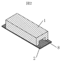
- FIG. 2 is a schematic diagram showing a groove structure 8 provided in the lid 1 containing a dielectric loss material.
- the cross section of the groove structure 8 is rectangular, and in this embodiment, the groove depth is at least four times the thickness of the high-frequency line dielectric portion provided on the circuit board 2, and the groove width is not more than the wavelength size of the used frequency. .
- it is a rectangle in the present invention, it can be constituted by an arc, a shape obtained by cutting a part of an ellipse, a triangle, a polygon, a free-form surface, or a cross-section obtained by combining these in combination.
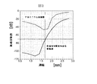
- Fig. 3 shows the result of analyzing the radio wave passage characteristics of the groove structure using an electromagnetic field simulator HFSS (a high frequency device design tool provided by Ansoft, Inc., USA as one of numerical electromagnetic field software).
- the horizontal axis represents the width of the groove structure 8
- the vertical axis represents the radio wave passage suppression value when radio waves are input from before and after the groove structure 8.
- a lid is placed on a 130 ⁇ m dielectric resin corresponding to the circuit board 2, and radio waves are input from before and after the groove.
- a radio wave 76 GHz (wavelength ⁇ 3.89 mm) was assumed.
- the cross section of the groove structure was rectangular, the depth of the groove was 0.8 mm, which is four times or more the dielectric thickness 130 ⁇ m, and the width was varied from 0.6 mm to 3.0 mm.
- the length of the groove is 8 mm.
- the lid for forming the groove was compared with an assumed material of aluminum metal (Metal Cover) and resin containing 50% by mass of graphite (Graphite % Cover).
- a 50% by mass graphite lid has a volume resistivity of about 1 M ⁇ , a reflection efficiency of 0.89, and an electrical property equivalent to a relative permittivity of 21 and a dielectric loss of 0.34.
- the radio wave When aluminum metal is used for the lid, the radio wave easily passes through the groove structure, and the maximum wave suppression value is -44 dB around 1.8 mm (equivalent to ⁇ / 2) corresponding to the cutoff frequency as a waveguide. .
- the cutoff frequency in a metal waveguide is c / (waveguide width * 2) (where c is the speed of light).
- FIG. 4 shows a groove structure 8 shown in FIG. 2, in which a high frequency line 3 (microstrip line is used in the data of FIG. 4) is provided on the circuit board 2, and the influence of the width of the groove structure on the microstrip line is analyzed. It is a result.
- the high frequency line 3 may be a coplanar line, a ground coplanar line, or a differential line.
- the groove width is 3.0 mm or less, the effect of proximity to the microstrip line can be confirmed by the cover groove structure.
- the passage loss of the microstrip line increases, but the passage loss increase amount is only about 0.7 dB when the groove width is 1.5 mm. For this reason, if the groove width is 1.5 mm or more, the influence of the passage loss can be substantially ignored.
- the line When connecting a signal having a frequency lower than the microwave to the millimeter-wave band high-frequency circuit 4 or the passive element 6, the line uses a conductor layer disposed on the inner layer of the circuit board, passes through the GND layer of the circuit board 2, and Connect the surface layer conductor and the inner layer conductor via.
- a conductor extraction pattern having a size less than 1 ⁇ 2 of the wavelength ⁇ of the use frequency is provided in the GND layer.
- the millimeter-wave band communication apparatus of the present invention shown in FIG. 1 is provided with a recess 5 and a groove structure 8 in a lid 1 containing a dielectric loss material and combined with a circuit board 2 so that the millimeter-wave band high-frequency circuit 4 can be While suppressing unwanted radio wave mixing, the irradiation to the millimeter wave band high frequency circuit 4 by the antenna side lobe is suppressed, the leakage wave emitted from the millimeter wave band high frequency circuit 4 itself is suppressed, and the lid concave portion in which the millimeter wave band high frequency circuit 4 is housed.
- the millimeter-wave band communication apparatus 10 can perform communication quality and high-sensitivity sensing utilizing high-performance reception sensitivity by drastically reducing the occurrence of unnecessary spurious and the like.
- the millimeter wave band communication device of the present invention shown in FIG. 1 has a lid recess 5 and a groove as means for reducing the distance between the lid surface and the circuit board.
- the structure 8 is provided, multiple reflection attenuation due to the dielectric loss material is always obtained. Therefore, even a resin lid on the inner surface of the flat lid without the lid recess 5 and the groove structure 8 is practical if the radio wave suppression amount specification is small.
- the lid of the present invention is not a radio wave shield by metallic radiation (total reflection), but the radio wave is extinguished between the lid and the circuit board by moderate multiple reflection attenuation, so that the lid is electrically connected to the GND of the circuit board. do not have to. Therefore, it is not necessary to manage gaps with the circuit board, solder brazing, conductive adhesive, etc., as in the case of assembly with a metal lid, and the lid is screwed, pinned, fitted, pinched, insulative bonded It can be fixed by simple means such as an agent. If the lid is formed using a molding technique using a mold, the assembly cost and the lid processing cost can be greatly reduced.
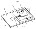
- FIG. 5 is a perspective view of a millimeter wave band communication apparatus according to the second embodiment of the present invention.
- 1 is a lid
- 2 is a circuit board
- 3 is a microstrip line
- 4 is a millimeter-wave band high-frequency circuit
- 5 is a lid recess
- 6 is a passive element
- 7 is an interlayer conductor
- 8-2 is a groove structure with a choke structure
- 9 is an antenna.
- the groove structure 8-2 is a groove structure provided in the lid 1 containing 20% or more of dielectric loss material.
- the groove width is narrowed to suppress the amount of radio wave propagation.
- the loss of the microstrip line increases as a side effect.
- the width of the groove structure is equal to or less than the wavelength ⁇ of the utilization frequency, but by providing a choke structure that narrows the cross-sectional area locally disposed in the groove structure, the influence on the microstrip line is reduced, Increased radio wave suppression effect in the groove structure itself.
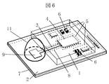
- FIG. 6 is a perspective view of a millimeter wave band communication apparatus according to a third embodiment of the present invention.
- 1 is a lid
- 2 is a circuit board
- 3 is a microstrip line
- 4 is a millimeter-wave band high frequency circuit
- 5 is a lid recess
- 6 is a passive element
- 7 is an interlayer conductor
- 8 is a groove structure of the lid
- 9 is an antenna
- 11 is a dielectric lens (lens antenna).
- the dielectric lens 11 is connected to the antenna 9 provided on the circuit board 2.
- the dielectric lens 11 is an insulator, and condenses radio waves on the lens curved surface to narrow the angle.
- a two-color molding method in which a single material is used to form both the lid and the lens, because an insulator with a different material from the lid and good radio wave transmission characteristics is used. It is possible to integrate by using a color mixing method or the like.
- the material for the lens antenna is formed only on the portion of the dielectric lens 11 through which radio waves pass and collects, and the material around the lid 1 is held and fixed around the lens, thereby eliminating the gap between the lid 1 and the dielectric lens 11.
- the radio wave radiated from the antenna 9 can be efficiently propagated without leaking outside the lens.
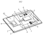
- FIG. 7 is a perspective view of a millimeter wave band communication apparatus according to the fourth embodiment of the present invention.
- 1 is a lid
- 2 is a circuit board
- 3 is a microstrip line
- 4 is a millimeter-wave band high frequency circuit
- 5 is a lid recess
- 6 is a passive element
- 7 is an interlayer conductor
- 8 is a groove structure of the lid
- 9 is an antenna
- 12 are waveguide type horn antennas.
- the horn antenna 12 is connected to the antenna 9 provided on the circuit board 2.
- the horn antenna 12 can be processed with a resin in which a dielectric loss material is highly blended like the lid 1. Similar to the lens antenna of the third embodiment, the horn antenna 12 and the lid 1 can be integrated to simplify the holding and fixing of the horn antenna.
- a resin having a graphite compounding ratio exceeding 80% by mass so as to suppress attenuation due to multiple reflections on the inner surface of the horn antenna may be produced by a two-color molding method as in the lens antenna.
- FIG. 8 is a perspective view of a millimeter wave band communication apparatus according to the fifth embodiment of the present invention.
- 1 is a lid
- 2 is a circuit board
- 3 is a microstrip line
- 4 is a millimeter-wave band high-frequency circuit
- 5 is a lid recess
- 6 is a passive element
- 7 is an interlayer conductor
- 8 is a groove structure of the lid
- 12 is a horn
- An antenna 13 is a slit
- 14 is a slot
- 15 is a via.
- the microstrip line 3, the slit 13, and the slot 14 are formed on the circuit board 2.
- the microstrip line 3 uses the interlayer conductor 7 as the GND conductor, but the slit 13 is provided in the interlayer conductor 7 of the GND conductor.
- the millimeter wave signal transmitted from the millimeter wave band high frequency circuit 4 is propagated to the horn antenna 12 on the opposite side of the circuit board 2 through the microstrip line 3, the slit 13 and the slot 14.
- the microstrip line in which the GND conductor is cut out by the via 15 and the slit 13 is inductive and has a structure in which radiation leakage is likely to occur.
- a concave portion 5 of the lid 1 is provided in the line conversion portion of the microstrip line-slit. Radiation leakage is reduced by the recess 5 of the lid 1 covering the line converter.
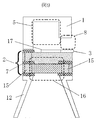
- FIG. 9 is a cross-sectional view of the millimeter waveband communication apparatus of the sixth embodiment of the present invention.
- 1 is a lid
- 2 is a circuit board
- 3 is a microstrip line
- 5 is a lid recess
- 7 is an interlayer conductor
- 8 is a groove structure of the lid
- 12 is a horn antenna
- 16 is a waveguide imitated in the circuit board.
- the structure 17 is a stub line having a length of ⁇ / 4.
- the microstrip line 3 is connected to a stub line 17 disposed on the waveguide structure 16.
- the lid recess 5 disposed in the waveguide structure 16 and the stub line 17 is formed with a groove having a depth of ⁇ / 4.
- the lid recess 5 serves as a ⁇ / 4 waveguide back short so that the line is efficiently converted from the microstrip line 3 to the waveguide structure 16 via the stub line 17.
- the lid 1 in which the dielectric loss material is highly blended in Examples 1 to 6 is made of a material having reflection loss characteristics while suppressing radio wave transmission characteristics.
- the millimeter-wave band high-frequency circuit 4 provided on the circuit board 2 in the lid recess 5 unnecessary radio waves from the outside are suppressed by the radio wave transmission characteristics of the lid 1.
- Unwanted radio waves that enter after being reflected through the gap between the lid 1 and the circuit board 2 are attenuated and extinguished by multiple reflections between the circuit board 2 and the lid 1.
- the isolation between the lid concave portion 5 covering the millimeter wave band high frequency circuit 4 is a radio wave transmission characteristic of the lid 1 itself, and the radiation leakage radio wave from the millimeter wave band high frequency circuit 4 itself is attenuated by multiple reflection due to the internal reflection of the lid concave portion 5. Disappear.
- the signal transmission to the antenna 9 and the outside is connected via a line provided in the groove 8 of the lid 1.
- Radio wave propagation is possible even with the groove structure itself of the lid 1, but by limiting the width of the groove 8 to ⁇ or less, it is possible to suppress radio wave propagation by increasing the multiple reflection attenuation in the groove space. Sufficient isolation can be obtained.
- the lid thickness is controlled by the lid thickness.
- the electromagnetic wave is suppressed by the multiple reflection attenuation between the lid and the circuit board, so that it is not necessary to electrically connect the lid and the GND of the circuit board. Therefore, the lid 1 only needs to be physically in contact with the circuit board 2.
- the lid 1 can be easily assembled by screwing, pinning, insulating adhesive, etc., and the mounting cost is extremely low compared to the metal lid. Realized at low cost.
- the present invention is not limited to the above-described embodiment, and includes various modifications.
- a part of the configuration of one embodiment can be replaced with the configuration of another embodiment, and the configuration of another embodiment can be added to the configuration of one embodiment.
- the present invention can be used for communication devices and sensor devices that use millimeter wave electromagnetic waves.
Landscapes
- Engineering & Computer Science (AREA)
- Microelectronics & Electronic Packaging (AREA)
- Physics & Mathematics (AREA)
- Electromagnetism (AREA)
- Aerials With Secondary Devices (AREA)
- Shielding Devices Or Components To Electric Or Magnetic Fields (AREA)
- Waveguide Aerials (AREA)
- Waveguides (AREA)
- Variable-Direction Aerials And Aerial Arrays (AREA)
- Radar Systems Or Details Thereof (AREA)
Abstract
外部から不要電波を遮蔽する蓋において、空間共振が発生しないミリ波帯通信装置を提案する。 基板と、基板上に設けられたミリ波帯用の高周波回路素子と、高周波回路素子と基板表面の少なくとも一部を覆うバルク材からなる蓋が設けられ、蓋は基体に誘電損失材料を配合して構成されていることを特徴とするミリ波帯通信装置が開示される。
Description
本発明は、ミリ波帯電磁波を利用して行う通信装置およびセンサ装置に関するものである。
ミリ波帯周波数を利用した装置は広帯域性から無線基地局間のバックボーン回線装置への応用が、また、鋭い直進性からレーダ等のセンシング装置への応用が期待されている。近年のミリ波帯半導体デバイスは送信回路、あるいは受信回路、もしくはその両方の機能が1つのパッケージ内に集積され、ボールグリッドアレイなどの表面実装用端子形態で市場へ支給されている。よって、これらデバイスを用いた製品は部品実装マウンターとリフロー炉を用いることが前提となり、ミリ波帯向けの製品においても低コストでの組立が実現されている。
ミリ波レーダに用いられるミリ波帯半導体デバイスは信号ダイナミックレンジが広く高感度なデバイスである。半導体デバイスの誤動作の要因として外部からの不要電波の混信があり、不要電波の抑制策として、特許文献1~特許文献4に示すように、金属性の蓋を用いたシールドケースが用いられている。
背景技術に示されるミリ波帯通信装置は外界からの不要電波の抑制策として金属蓋(シールドケース)を用いる。シールドケースは、金属の高い導電率により電波が輻射される効果(二次輻射)を利用し、電波を反射する。金属の高い反射効率は、ケース内では電波の空間共振が発生しやすいことを示し、ミリ波帯の回路自身から放射漏洩する電波により受信回路や発振器に悪影響を受ける可能性がある。
特許文献1では共振周波数が使用周波数を避けるようシールドケースの空間サイズを設定する。特許文献2では空間に設けた金属突起の周期構造におけるバンドストップフィルタを利用する。特許文献3は電磁波吸収性熱可塑性材料(以下電波吸収体と略す)を用いて空間共振を抑制可能である。しかしながら、所望の電波透過特性は電波吸収体単独では達成できないため、外部からの不要電波抑制や複数のミリ波帯高周波回路間のアイソレーションのために、別途金属の蓋やケース内仕切り板が必要である。
特許文献4では誘電体基板上のミリ波帯高周波回路動作に不要な範囲に抵抗層を形成し、シールドケースのQ値を低下させ、不要な共振や発振を低減する。電波吸収体や抵抗膜は媒体表面で反射することを避けるため、空気との特性インピーダンス差が小さい低誘電率の材料を用い、電波が媒体内部の損失性材料に到達するよう工夫されている。
これらの事例では、金属蓋と共に空間共振抑制のための工夫を必須とし、部材コストが高いという問題は残る。さらに、金属蓋の使用を前提としたシールド構造は、穴やスリットがあると電波が漏洩することから、これらを極力塞がなければならず、金属蓋の封止方法も課題である。
本発明の一側面は、基板と、基板上に設けられたミリ波帯用の高周波回路素子と、高周波回路素子と基板表面の少なくとも一部を覆うバルク材からなる蓋が設けられ、蓋は基体に誘電損失材料を配合して構成されていることを特徴とするミリ波帯通信装置である。
本発明の他の一側面は、基板と、基板上に設けられた高周波回路素子と、高周波回路素子と基板表面の少なくとも一部を覆う蓋と、を備え、蓋は、基体に誘電損失材料を質量比で20%以上80%以下混合して一体成型したものであり、その体積抵抗率は20Ω・cm以上であり、電波反射効率を90%以下としたことを特徴とするミリ波帯通信装置である。
外部からの不要電波を抑止するとともに、ミリ波帯高周波回路自身からの放射漏洩電波を低減できる、ミリ波帯通信装置が低コストで実現される。
実施の形態について、図面を用いて詳細に説明する。ただし、本発明は以下に示す実施の形態の記載内容に限定して解釈されるものではない。本発明の思想ないし趣旨から逸脱しない範囲で、その具体的構成を変更し得ることは当業者であれば容易に理解される。
以下に説明する発明の構成において、同一部分又は同様な機能を有する部分には同一の符号を異なる図面間で共通して用い、重複する説明は省略することがある。
図面等において示す各構成の位置、大きさ、形状、範囲などは、発明の理解を容易にするため、実際の位置、大きさ、形状、範囲などを表していない場合がある。このため、本発明は、必ずしも、図面等に開示された位置、大きさ、形状、範囲などに限定されない。
以下で説明する実施例では、電磁波透過特性を抑える手段として、金属あるいは金属メッキの蓋の代替に、誘電損失材料を配合した蓋を利用する。誘電損失材料を配合することにより、蓋の電波反射率を90%以下になるようにする。電波反射特性が主に蓋表面の特性に依存する場合には、蓋表面での電波反射効率を金属的な全反射でなく少なくとも90%以下となるよう蓋の表面抵抗を上げる。蓋の反射率を下げることにより、反射の際に損失を生じさせることができるので、多数回反射させることによる電波の減衰効果を得ることができる。減衰効果は、反射率の反射回数乗で計算できる。
蓋の反射率を下げると、電波の通過損失改善のために蓋厚みを増す必要がある。蓋厚みの増大は、製品の容積や重量増大、製造コスト上昇につながるため、蓋厚みは薄いほうが望ましい。このため、蓋の電波反射率は50%以上が望ましい。
誘電損失材料には例えば黒鉛粉を用い、その形状は特に限定しないが、鱗片状、球状、楕円状、針状、紐状及び不定形又は前記形状の混合粉であり、平均粒径は例えば200μm以下とする。
蓋に配合される誘電損失材料の配合比は、所望の電波反射効率を得るように調整する。蓋の電波反射効率を90%以下にするためには、誘電損失材料の配合比を、蓋全体あるいは平均の質量比で例えば、20%以上80%以下とし、蓋全体あるいは平均の体積抵抗率は20Ω・cm以上とする。誘電損失材料の配合比率を高め体積抵抗率を下げると、電波透過量が低下し反射効率が増加する。
蓋の組成を均一にした場合には、例えば、蓋表面の電波反射効率が90%以下、誘電損失材料の配合比を、蓋表面で例えば、20%以上80%以下とする。
蓋の内側に発生または進入した電波は、蓋と回路基板間の多重反射により電波を減衰するため、蓋の内側表面と回路基板を近づける構成とする。
例えば半導体チップで構成されるミリ波帯高周波回路を回路基板表面に実装した場合、ミリ波帯高周波回路を覆うための蓋の外形高さは、ミリ波帯高周波回路の高さ以上必要になる。蓋が一体形成のバルク材の場合には、ミリ波帯高周波回路の凸部に応じて蓋に凹部(キャビティ)を設けると、その凹部にミリ波帯高周波回路を収納し覆い隠すことで蓋を回路基板に密着するほど接近させることができる。
一方、誘電損失材料を配合した蓋は近接するだけでミリ波信号が減衰するため、蓋が電波の伝送線路に近づき過ぎないよう溝を設けることが望ましい。溝の最深部は回路基板に形成された線路を形成する誘電体厚さの4倍以上であり、溝の幅は利用周波数の空間波長λ以下とすることが望ましい。
上記の凹部や溝は、誘電損失材料を配合した樹脂等によって蓋を一体成型することにより、低コストで容易に製造することができる。
回路基板には蓋へ電波を反射する金属層が形成され、その一部をミリ波帯高周波回路のGNDとして利用することができる。
<1.ミリ波帯通信装置の全体構造>
図1は本発明の第1の実施例のミリ波帯通信装置の斜視図である。1は蓋であり、2は回路基板、3は高周波線路、4はミリ波帯高周波回路(能動素子)、5は蓋凹部、6は受動素子、7は層間導体、8は蓋の溝構造、9はアンテナである。ミリ波帯高周波回路4が生成するミリ波は、例えば76GHzで波長は4mm程度である。
図1は本発明の第1の実施例のミリ波帯通信装置の斜視図である。1は蓋であり、2は回路基板、3は高周波線路、4はミリ波帯高周波回路(能動素子)、5は蓋凹部、6は受動素子、7は層間導体、8は蓋の溝構造、9はアンテナである。ミリ波帯高周波回路4が生成するミリ波は、例えば76GHzで波長は4mm程度である。
高周波線路3とアンテナ9は回路基板2の表面に形成され、層間導体7は回路基板2の内層に形成され、その一部の導体層は高周波線路3のGND電極(接地電極)として機能する。蓋1は回路基板2の表面に配置する。回路基板2の側からの外部電波の進入を防止するために、通常GND電極はシールドの効果を持つように構成される。シールドは、回路基板2の両側(表と裏)で電波を反射するように機能する。高周波線路3はミリ波帯高周波回路4とアンテナ9を接続する。このような構成により、ミリ波帯高周波回路4が生成するミリ波は、アンテナ9から放射される。
<2.蓋の構造>
蓋1は樹脂に黒鉛など誘電損失材料を配合した材料で形成する。例えば、熱可塑樹脂に誘電損失材料を配合し、射出形成することにより容易に製造が可能である。その黒鉛の形状は鱗片状、球状、楕円状、針状、紐状のいずれでもよい。また不定形又は前記形状の混合粉でもよい。誘電損失材料は微細なほうが均一な特性を得られるが、製造の容易性も考慮し、本実施例では平均粒径を200μm以下とする。本実施例では、蓋に配合される誘電損失材料の配合比は、質量比で20%以上80%以下として均一に分布するものとし、表面抵抗率は20Ω以上とする。
蓋1は樹脂に黒鉛など誘電損失材料を配合した材料で形成する。例えば、熱可塑樹脂に誘電損失材料を配合し、射出形成することにより容易に製造が可能である。その黒鉛の形状は鱗片状、球状、楕円状、針状、紐状のいずれでもよい。また不定形又は前記形状の混合粉でもよい。誘電損失材料は微細なほうが均一な特性を得られるが、製造の容易性も考慮し、本実施例では平均粒径を200μm以下とする。本実施例では、蓋に配合される誘電損失材料の配合比は、質量比で20%以上80%以下として均一に分布するものとし、表面抵抗率は20Ω以上とする。
黒鉛の配合比が80%を超えて成型した場合、体積抵抗率が10Ω以下となり蓋の電波遮蔽効果は増大するが、体積抵抗率と比例して表面抵抗率も低下し蓋表面での反射効率は1に近く、電波はほぼ全反射する。
全反射に近い蓋は、蓋1の外側からの電波を遮蔽するためには好ましい一方、蓋1の内側(ミリ波帯高周波回路4などが配置されている側)の電波については、反射時にほとんど電波が減衰しないため、空間共振の消滅は困難である。そこで本実施例では、蓋の誘電損失材料の配合比率を80%以下とし、蓋表面の反射効率をあえて90%以下に抑えることにより、電波が蓋の内側で反射する際の減衰を大きくする。さらに、複数回電波を反射させることによる多重反射減衰で空間共振の消滅を図っている。
多重反射減衰のためには、ミリ波帯高周波回路4を囲む電波反射面間の距離を小さくすることが有利である。図1に示す例では、蓋1は回路基板2に垂直方向に厚みTを有しており、ミリ波帯高周波回路4などの高周波回路素子を覆うように凹部5を設けている。
多重反射減衰のため、蓋1の凹部5の天井(蓋1の回路基板2と対向する表面)と回路基板2との距離Dは、厚みTより小さく構成されており、反射面である天井と基板の距離Dを小さくすることにより、反射回数を増加させている。蓋1が図1に示すような概略直方体のバルク形状の場合、その寸法の一例を示せば、蓋1の縦横は3~5cm程度である。また、蓋1の厚みTは2mm程度であり、上記距離Dはミリ波帯高周波回路4の高さHより大きく厚みTより小さい。
蓋に黒鉛と混合されるバインダー材(基体)には樹脂あるいはセラミックを用い、黒鉛により蓋の体積抵抗率を変更できるよう絶縁性の材料を用いることが望ましい。蓋1のバインダー材とする樹脂等は例えばフェノール樹脂など公知の種々の材料が利用可能であり、製造方法も射出形成に限らない。
蓋1内部の誘電損失材は、回路基板2に近いほど配合濃度を下げた蓋や、厚み中心部分の配合濃度を高め表面に近いほど濃度を下げた蓋など、蓋反射効率を90%以下にするための誘電損失材料濃度は均等でなくてもよい。このように誘電損失材の濃度に分布を設けることにより、蓋の外側で電波を反射しやすくし、蓋の内側で電波を反射しにくくするように構成することもできる。また、蓋の表面では電波を反射しにくくしつつ、蓋の内部で電波を遮蔽することもできる。
<3.蓋凹部(キャビティ)の構造>
図1に示すミリ波帯通信装置の蓋1は、先に述べたように基本的にはバルク材であり、回路基板2の垂直方向に所定の厚みTを持つ直方体形状である。先に述べたように、蓋1にはミリ波帯高周波回路4と受動素子6を配置するための蓋凹部(キャビティ)5を設けている。回路基板2に実装したミリ波帯高周波回路4と受動素子6により回路基板2の表面は凹凸が生じるが、蓋1に設けた蓋凹部にミリ波帯高周波回路4の凸部を勘合させることで、蓋1内側表面と回路基板2の距離を短縮し、多重反射を生じやすくする。また、蓋1と回路基板2が密着することにより、外部からキャビティ内への電波の進入を防止する。先に述べたように、蓋1は一体成型されているため、蓋1の外側の表面と裏側の表面(蓋凹部5の表面)は連続した面となる。
図1に示すミリ波帯通信装置の蓋1は、先に述べたように基本的にはバルク材であり、回路基板2の垂直方向に所定の厚みTを持つ直方体形状である。先に述べたように、蓋1にはミリ波帯高周波回路4と受動素子6を配置するための蓋凹部(キャビティ)5を設けている。回路基板2に実装したミリ波帯高周波回路4と受動素子6により回路基板2の表面は凹凸が生じるが、蓋1に設けた蓋凹部にミリ波帯高周波回路4の凸部を勘合させることで、蓋1内側表面と回路基板2の距離を短縮し、多重反射を生じやすくする。また、蓋1と回路基板2が密着することにより、外部からキャビティ内への電波の進入を防止する。先に述べたように、蓋1は一体成型されているため、蓋1の外側の表面と裏側の表面(蓋凹部5の表面)は連続した面となる。
<4.高周波線路と溝構造>
ミリ波帯高周波回路4から生成されたミリ波信号は、高周波線路3によりアンテナ9に導かれる。誘電損失材料を配合した蓋1は近接するだけでミリ波信号が減衰するため、蓋1が高周波線路3に近づき過ぎないよう溝8を設けることが望ましい。一方、外部からの電波が溝8を経由してキャビティ5内に進入したり、不要の電波が溝8を経由して外部に漏洩したりしない設計が望ましい。このためには、溝8の最深部は回路基板2に形成された高周波線路3を形成する誘電体厚さの4倍以上であり、溝8の幅は利用周波数の空間波長λ以下とすることが望ましい。
ミリ波帯高周波回路4から生成されたミリ波信号は、高周波線路3によりアンテナ9に導かれる。誘電損失材料を配合した蓋1は近接するだけでミリ波信号が減衰するため、蓋1が高周波線路3に近づき過ぎないよう溝8を設けることが望ましい。一方、外部からの電波が溝8を経由してキャビティ5内に進入したり、不要の電波が溝8を経由して外部に漏洩したりしない設計が望ましい。このためには、溝8の最深部は回路基板2に形成された高周波線路3を形成する誘電体厚さの4倍以上であり、溝8の幅は利用周波数の空間波長λ以下とすることが望ましい。
図2は誘電損失材料を配合した蓋1に設けられた溝構造8を示す模式図である。溝構造8断面は長方形形状であり、本実施例では、溝深さは回路基板2に設けられた高周波線路誘電体部分の厚みの4倍以上とし、溝幅は利用周波数の波長サイズ以下とする。本発明では長方形であるが、円弧、楕円の一部をカットした形、三角形、多角形、自由曲面、これらを複合的に組み合わせた断面で構成することができる。
図3は電磁界シミュレータHFSS(数値電磁界ソフトのひとつとして,米国 Ansoft社が提供している高周波デバイス設計ツール)を用いて溝構造の電波通過特性を解析した結果である。横軸は溝構造8の幅、縦軸は溝構造8の前後より電波を投入した場合の電波の通過抑制値である。
回路基板2に相当する130μmの誘電体樹脂の上に蓋を設け、溝の前後より電波を投入する。電波としては、76GHz(波長λ≒3.89mm)を想定した。溝構造の断面は長方形であり、溝の深さは誘電体厚さ130μmの4倍以上である0.8mmとし、幅は0.6mmから3.0mmまで寸法を変化させた。溝の長さは8mmである。溝を形成する蓋はアルミニウム金属(Metal Cover)と黒鉛を50質量%含む樹脂(Graphite Cover)を想定材料として比較した。黒鉛の50質量%の蓋は体積抵抗率1MΩ程度、反射効率は0.89、電気的物性として比誘電率21、誘電損失0.34に相当する。Keysight製材料測定ソフトウェア85071E(商品名)の伝送ライン法による計測結果を用いた。
アルミニウム金属を蓋に用いた場合、電波は溝構造を容易に通過し、導波管として遮断周波数に相当する幅=1.8mm(λ/2相当)前後で通過抑制値が最大となり-44dBである。なお、公知のように金属導波管における遮断周波数はc/(導波管幅*2)である(ただし、cは光速)。金属蓋の場合、溝構造8以外に回路基板2を構成する130umの樹脂内を透過する電波が存在する。回路基板2のGND導体と金属蓋を隙間なく接続しない限り、電波漏洩が発生する。
金属蓋に対し、黒鉛を配合した蓋では溝構造内および蓋と回路基板間で多重反射減衰し、幅=2.8mmで-20dB、幅=1.8mmで-60dB、幅=1.5mm以下では-90dBまで減衰する。この結果から、黒鉛を配合した蓋では、蓋の溝幅が波長サイズ以下の場合に多重反射減衰によって空間電波伝播を大幅に抑制することと、蓋の透過伝搬量は-90dB以下に抑制されていることを確認できる。
図4は図2に示した溝構造8において、回路基板2に高周波線路3(図4のデータではマイクロストリップ線路を用いた)を設け、溝構造の幅によるマイクロストリップ線路への影響を解析した結果である。高周波線路3にはマイクロストリップ線路以外に、コプレーナ線路、グランドコプレーナ線路、差動線路を用いてもよい。溝幅3.0mm以下で、蓋溝構造によりマイクロストリップ線路に近接した影響を確認できる。誘電損失材料の影響を受け、マイクロストリップ線路の通過損失は増加するが、通過損失増加量は溝幅=1.5mmで0.7dB程度と軽微である。このため、溝幅が1.5mm以上であれば、通過損失の影響を実質的に無視できる。
マイクロ波以下の周波数の信号をミリ波帯高周波回路4や受動素子6へ接続する際、線路は回路基板内層に配置した導体層を用い、回路基板2のGND層を貫通して回路基板2の表層導体と内層導体をvia接続する。GND層をvia接続で貫通する際、利用周波数の波長λの1/2サイズ未満の導体抜きパターンをGND層に設ける。
図1に示す本発明のミリ波帯通信装置は、誘電損失材料を配合した蓋1に凹部5と溝構造8を設け回路基板2と組み合わせることで、ミリ波帯高周波回路4への外部からの不要電波混入を抑止しつつ、アンテナサイドローブによるミリ波帯高周波回路4への照射抑制、ミリ波帯高周波回路4そのものから発する漏洩電波の抑圧、ミリ波帯高周波回路4が収納された蓋凹部での空間共振の抑制、ミリ波帯高周波回路4から受動素子6等への電波クロストークの抑圧が可能となり、誤動作を誘引する不要電波が低減される。従って、ミリ波帯通信装置10は、不要なスプリアス等の発生が激減することで、高性能な受信感度を活かした通信品質や高感度なセンシングが可能となる。
図1に示す本発明のミリ波帯通信装置は、蓋1と回路基板2による多重反射減衰を効果的に得るために、蓋表面と回路基板の間の距離を縮める手段として蓋凹部5と溝構造8を設けたが、誘電損失材料による多重反射減衰は常に得られるため、蓋凹部5と溝構造8のないフラットな蓋内面の樹脂製蓋でも電波抑制量仕様が小さければ実用可能である。
本発明の蓋は金属的な輻射(全反射)による電波シールドではなく、適度な多重反射減衰により蓋と回路基板間で電波を消滅させているため、蓋を回路基板のGNDと電気的に接続する必要はない。従って、金属蓋との組み立てのように回路基板との隙間管理や半田ろう付け、導電性接着材などの加工も不要となり、蓋は、ねじ止め、ピン止め、はめ込み止め、挟み込み止め、絶縁性接着剤など簡便な手段で固定が可能である。蓋を金型による成型技術を用いて形成すれば、組み立て工費ともに蓋加工費も大幅な低コスト化が図れる。
図5は本発明の第2の実施例のミリ波帯通信装置の斜視図である。1は蓋であり、2は回路基板、3はマイクロストリップ線路、4はミリ波帯高周波回路、5は蓋凹部、6は受動素子、7は層間導体、8-2はチョーク構造付溝構造、9はアンテナである。
実施例1との際について説明する。溝構造8-2は誘電損失材料を20%以上配合される蓋1に設けられた溝構造であるが、図3、図4に示したように電波伝搬量抑制のために溝の幅を狭小化するとマイクロストリップ線路の損失が副作用的に増加する。この例では溝構造の幅は利用周波数の波長λ以下であるが、溝構造内に局所的に配置した断面積を狭くするチョーク構造を設けることで、マイクロストリップ線路への影響を緩和しつつ、溝構造そのものにおける電波抑制効果を高めた。
図6は本発明の第3の実施例のミリ波帯通信装置の斜視図である。1は蓋であり、2は回路基板、3はマイクロストリップ線路、4はミリ波帯高周波回路、5は蓋凹部、6は受動素子、7は層間導体、8は蓋の溝構造、9はアンテナ、11は誘電体レンズ(レンズアンテナ)である。
アンテナ9の放射指向性を高めるため、回路基板2に設けたアンテナ9に誘電体レンズ11を接続する。誘電体レンズ11は絶縁体であり、レンズ曲面にて電波を集光させ狭角化する。蓋と材質が異なり電波透過特性のよい絶縁体を採用するため、単一材料にて蓋とレンズの両方を形成することはないが、複数の材料を1つの金型で成形する二色成形法や混色成形法などを用いて一体化することは可能である。レンズアンテナ向けの材料は電波が通過し集光する誘電体レンズ11の部分のみ形成し、蓋1側の材料でレンズ周りを保持固定することで、蓋1と誘電体レンズ11の隙間をなくし、アンテナ9から放射された電波をレンズ外に漏洩することなく効率的に伝播可能である。
図7は本発明の第4の実施例のミリ波帯通信装置の斜視図である。1は蓋であり、2は回路基板、3はマイクロストリップ線路、4はミリ波帯高周波回路、5は蓋凹部、6は受動素子、7は層間導体、8は蓋の溝構造、9はアンテナ、12は導波管型ホーンアンテナである。
アンテナ9の放射指向性を高めるため、回路基板2に設けたアンテナ9にホーンアンテナ12を接続する。ホーンアンテナ12は蓋1と同じく誘電損失材料を高配合した樹脂で加工可能である。実施例3のレンズアンテナと同様にホーンアンテナ12と蓋1を一体化し、ホーンアンテナの保持固定を簡略化可能である。ホーンアンテナの内面で多重反射による減衰を抑えるよう黒鉛配合比が80質量%を超えた樹脂を、レンズアンテナと同様に二色成形法で作製してもよい。
図8は本発明の第5の実施例のミリ波帯通信装置の透視斜視図である。1は蓋であり、2は回路基板、3はマイクロストリップ線路、4はミリ波帯高周波回路、5は蓋凹部、6は受動素子、7は層間導体、8は蓋の溝構造、12はホーンアンテナ、13はスリット、14はスロット、15はviaである。マイクロストリップ線路3、スリット13、スロット14は回路基板2に形成され、マイクロストリップ線路3は層間導体7をGND導体として利用するが、スリット13はそのGND導体の層間導体7に設けられる。
ミリ波帯高周波回路4から送出されるミリ波信号はマイクロストリップ線路3、スリット13、スロット14を介して、回路基板2の反対側にあるホーンアンテナ12に伝播される。マイクロストリップ線路3からスリット13にミリ波を伝播させる際、via15を通して接続するが、via15とスリット13によってGND導体がくり貫かれたマイクロストリップ線路はインダクタンス性であり、放射漏洩しやすい構造である。このマイクロストリップ線路-スリットの線路変換部に蓋1の凹部5を設ける。蓋1の凹部5が線路変換部を覆うことで、放射漏洩を低減する。
図9は本発明の第6の実施例のミリ波帯通信装置の断面図である。1は蓋であり、2は回路基板、3はマイクロストリップ線路、5は蓋凹部、7は層間導体、8は蓋の溝構造、12はホーンアンテナ、16は回路基板内に模造した導波管構造、17はλ/4長さのスタブ線路である。マイクロストリップ線路3は導波管構造16上部に配置されたスタブ線路17に接続される。導波管構造16およびスタブ線路17に配置される蓋凹部5は、深さλ/4の溝が形成される。スタブ線路17を介して、マイクロストリップ線路3から導波管構造16に効率よく線路変換されるよう蓋凹部5はλ/4の導波管バックショートとして働く。
以上詳細に説明したように、本実施例1~6において誘電損失材を高配合した蓋1は、電波透過特性を抑制しつつ、反射損失特性を有する材料からなる。回路基板2に設けたミリ波帯高周波回路4を蓋凹部5に収納することで、蓋1の電波透過特性にて外部からの不要電波を抑止する。蓋1と回路基板2との隙間を反射して侵入する不要電波は回路基板2と蓋1との多重反射により減衰消滅する。ミリ波帯高周波回路4を覆う蓋凹部5間のアイソレーションは蓋1そのものの電波透過特性であり、ミリ波帯高周波回路4自身からの放射漏洩電波は蓋凹部5の内面反射により多重反射減衰し消滅する。
アンテナ9および外部への信号伝達は蓋1の溝8内に設けた線路を介して接続する。蓋1の溝構造そのものでも電波伝播は可能であるが、溝8の幅をλ以下に制限することで、溝空間での多重反射減衰を増すことにより電波伝播抑制は可能であり、回路間の十分なアイソレーションを得られる。
また、樹脂内の誘電損失材の配合比を選択することで、透過特性と反射特性のバランスを調整し、蓋厚みにより透過特性の増減を制御する。金属蓋のシールド効果と違い、蓋と回路基板間の多重反射減衰により電磁波を抑制するため、蓋と回路基板のGNDと電気的に接続する必要はない。従って、蓋1は回路基板2に物理的に接していればよく、蓋1はねじ留めやピン止め、絶縁性接着剤などにより簡易組立が可能であり、実装コストは金属蓋と比較して極めて低コストで実現される。
本発明は上記した実施形態に限定されるものではなく、様々な変形例が含まれる。例えば、ある実施例の構成の一部を他の実施例の構成に置き換えることが可能であり、また、ある実施例の構成に他の実施例の構成を加えることが可能である。また、各実施例の構成の一部について、他の実施例の構成の追加・削除・置換をすることが可能である。
本発明は、ミリ波帯電磁波を利用して行う通信装置およびセンサ装置に利用することができる。
1 蓋
2 回路基板
3 高周波線路(マイクロストリップ線路)
4 ミリ波帯高周波回路
5 蓋凹部
6 受動素子
7 層間導体
8 溝構造
8-2 チョーク構造付溝構造
9 アンテナ
10 ミリ波帯通信装置
11 誘電体レンズ
12 ホーンアンテナ
13 スリット
14 スロット
15 via
16 導波管構造
17 スタブ線路
2 回路基板
3 高周波線路(マイクロストリップ線路)
4 ミリ波帯高周波回路
5 蓋凹部
6 受動素子
7 層間導体
8 溝構造
8-2 チョーク構造付溝構造
9 アンテナ
10 ミリ波帯通信装置
11 誘電体レンズ
12 ホーンアンテナ
13 スリット
14 スロット
15 via
16 導波管構造
17 スタブ線路
Claims (15)
- 基板と、
前記基板上に設けられたミリ波帯用の高周波回路素子と、
前記高周波回路素子と前記基板表面の少なくとも一部を覆うバルク材からなる蓋が設けられ、
前記蓋は基体に誘電損失材料を配合して構成されていることを特徴とするミリ波帯通信装置。 - 前記誘電損失材料は黒鉛であることを特徴とする請求項1記載のミリ波帯通信装置。
- 前記蓋の電波反射効率を90%以下とすることを特徴とする請求項1記載のミリ波帯通信装置。
- 前記蓋の電波反射効率を50%以上90%以下とすることを特徴とする請求項1記載のミリ波帯通信装置。
- 前記蓋は前記基体として樹脂を用い、一体で成型されていることを特徴とする請求項1記載のミリ波帯通信装置。
- 前記蓋に配合される前記誘電損失材料の配合比は、蓋全体あるいは平均の質量比で20%以上80%以下であることを特徴とする請求項1記載のミリ波帯通信装置。
- 前記蓋の体積抵抗率を20Ω・cm以上とすることを特徴とする請求項1記載のミリ波帯通信装置。
- 前記誘電損失材料は、前記蓋の前記基板に対向する側ほど配合濃度を下げたことを特徴とする請求項1記載のミリ波帯通信装置。
- 前記誘電損失材料は、前記蓋の厚み中心ほど配合濃度を上げたことを特徴とする請求項1記載のミリ波帯通信装置。
- 前記蓋は直方体であり、前記基板に垂直方向に厚みTを有し、前記高周波回路素子を覆うように凹部を有し、前記蓋の凹部の天井と前記基板との距離Dは、前記厚みTより小さく、かつ、前記高周波回路素子の高さHよりも大きく構成されている請求項1記載のミリ波帯通信装置。
- 前記基板表面に設けられ、前記高周波回路素子に接続された高周波線路と、
前記高周波線路と前記蓋が接しないよう前記蓋に形成された溝構造を有する請求項1記載のミリ波帯通信装置。 - 前記高周波線路の電波伝播方向と交差する断面の前記溝構造の幅を、ミリ波利用周波数の波長λ以下とすることを特徴とする請求項11記載のミリ波帯通信装置。
- 前記高周波線路の前記高周波回路素子と反対側に設けられたアンテナと、
絶縁体で構成された誘電体レンズを備え、
前記蓋と前記誘電体レンズが一体で構成されていることを特徴とする請求項11記載のミリ波帯通信装置。 - 前記高周波線路の前記高周波回路素子と反対側に設けられたアンテナと、
樹脂に誘電損失材料を配合して構成されたホーンアンテナを備え、
前記蓋と前記ホーンアンテナが一体で構成されていることを特徴とする請求項11記載のミリ波帯通信装置。 - 前記蓋の凹部を深さλ/4とし、高周波線路の線路変換器のバックショートとして機能させることを特徴とする請求項14記載のミリ波帯通信装置。
Priority Applications (3)
| Application Number | Priority Date | Filing Date | Title |
|---|---|---|---|
| DE112017002142.1T DE112017002142B4 (de) | 2016-06-14 | 2017-04-13 | Millimeterwellenband-kommunikationsgerät |
| US16/308,320 US10756426B2 (en) | 2016-06-14 | 2017-04-13 | Millimeter-wave band communication device |
| CN201780023796.4A CN109075419B (zh) | 2016-06-14 | 2017-04-13 | 毫米波段通信装置 |
Applications Claiming Priority (2)
| Application Number | Priority Date | Filing Date | Title |
|---|---|---|---|
| JP2016-117506 | 2016-06-14 | ||
| JP2016117506A JP6687469B2 (ja) | 2016-06-14 | 2016-06-14 | ミリ波帯通信装置 |
Publications (1)
| Publication Number | Publication Date |
|---|---|
| WO2017217098A1 true WO2017217098A1 (ja) | 2017-12-21 |
Family
ID=60664516
Family Applications (1)
| Application Number | Title | Priority Date | Filing Date |
|---|---|---|---|
| PCT/JP2017/015124 Ceased WO2017217098A1 (ja) | 2016-06-14 | 2017-04-13 | ミリ波帯通信装置 |
Country Status (5)
| Country | Link |
|---|---|
| US (1) | US10756426B2 (ja) |
| JP (1) | JP6687469B2 (ja) |
| CN (1) | CN109075419B (ja) |
| DE (1) | DE112017002142B4 (ja) |
| WO (1) | WO2017217098A1 (ja) |
Families Citing this family (12)
| Publication number | Priority date | Publication date | Assignee | Title |
|---|---|---|---|---|
| US11031699B2 (en) | 2018-02-09 | 2021-06-08 | Intel IP Corporation | Antenna with graded dielectirc and method of making the same |
| WO2020194652A1 (ja) * | 2019-03-28 | 2020-10-01 | 三菱電機株式会社 | シールドケース |
| JP6767591B1 (ja) * | 2019-06-10 | 2020-10-14 | 株式会社フジクラ | モード変換器、rfモジュール、及び携帯端末 |
| DE102020112787A1 (de) * | 2020-01-13 | 2021-07-29 | Infineon Technologies Ag | Hochfrequenz-Vorrichtung mit Hochfrequenz-Chip und Hohlleiterstruktur |
| CN111585029B (zh) * | 2020-05-07 | 2024-11-29 | 华南理工大学 | 一种毫米波低剖面高增益差分喇叭天线 |
| EP4089836A4 (en) * | 2020-11-12 | 2023-04-19 | Guangzhou Shiyuan Electronics Co., Ltd. | ANTENNA ARRANGEMENT AND ELECTRONIC DEVICE |
| JP7463980B2 (ja) * | 2021-02-15 | 2024-04-09 | 株式会社デンソー | 無線通信機 |
| WO2022178822A1 (en) * | 2021-02-26 | 2022-09-01 | Intel Corporation | Integrated circuit supports with microstrips |
| CN220856914U (zh) * | 2021-05-07 | 2024-04-26 | 株式会社村田制作所 | 天线元件以及电子设备 |
| WO2023053235A1 (ja) * | 2021-09-29 | 2023-04-06 | 三菱電機株式会社 | パッチアンテナ装置 |
| JP2024166722A (ja) * | 2023-05-19 | 2024-11-29 | 三菱電機株式会社 | アンテナ装置 |
| US20250350013A1 (en) * | 2024-05-13 | 2025-11-13 | Rohde & Schwarz Gmbh & Co. Kg | Electrical interconnection element, high-frequency waveguide module, electrical apparatus |
Citations (8)
| Publication number | Priority date | Publication date | Assignee | Title |
|---|---|---|---|---|
| JPS56111511U (ja) * | 1980-01-29 | 1981-08-28 | ||
| JPH054592U (ja) * | 1991-06-26 | 1993-01-22 | 鐘淵化学工業株式会社 | 高周波数帯域用電子機器内部回路の反射防止構造 |
| JP2001057507A (ja) * | 1999-08-18 | 2001-02-27 | Matsushita Electric Ind Co Ltd | 衛星受信用コンバータ |
| JP2003273569A (ja) * | 2002-03-15 | 2003-09-26 | Showa Electric Wire & Cable Co Ltd | 電波吸収体およびその製造方法 |
| JP2008252634A (ja) * | 2007-03-30 | 2008-10-16 | Maspro Denkoh Corp | 衛星受信用コンバータ |
| JP2009010458A (ja) * | 2007-06-26 | 2009-01-15 | Panasonic Electric Works Co Ltd | アンテナ装置 |
| JP2014143250A (ja) * | 2013-01-22 | 2014-08-07 | Murata Mfg Co Ltd | モジュール基板 |
| JP2015119295A (ja) * | 2013-12-18 | 2015-06-25 | 日本ピラー工業株式会社 | アンテナ用ユニット |
Family Cites Families (16)
| Publication number | Priority date | Publication date | Assignee | Title |
|---|---|---|---|---|
| JPH054592A (ja) * | 1991-06-26 | 1993-01-14 | Yanmar Agricult Equip Co Ltd | 走行作業機における走行クローラ装置 |
| JPH1160969A (ja) * | 1997-08-27 | 1999-03-05 | Nagoya Polymer:Kk | 電磁波遮蔽性複合材料 |
| WO2000019559A1 (en) * | 1998-09-30 | 2000-04-06 | Anritsu Corporation | Planar antenna and method for manufacturing the same |
| US6518932B1 (en) * | 1999-02-15 | 2003-02-11 | Communications Research Laboratory, Independent Administrative Institute | Radio communication device |
| JP2000278009A (ja) * | 1999-03-24 | 2000-10-06 | Nec Corp | マイクロ波・ミリ波回路装置 |
| JP3739230B2 (ja) * | 1999-04-26 | 2006-01-25 | 株式会社日立製作所 | 高周波通信装置 |
| JP3629399B2 (ja) * | 2000-04-18 | 2005-03-16 | シャープ株式会社 | アンテナ一体化マイクロ波・ミリ波モジュール |
| US6410847B1 (en) | 2000-07-25 | 2002-06-25 | Trw Inc. | Packaged electronic system having selectively plated microwave absorbing cover |
| JP2002124592A (ja) | 2000-10-16 | 2002-04-26 | Sharp Corp | 高周波装置 |
| WO2003107729A1 (en) | 2002-06-14 | 2003-12-24 | Laird Technologies, Inc. | Composite emi shield |
| JP2007116217A (ja) * | 2005-10-18 | 2007-05-10 | Hitachi Ltd | ミリ波レーダ装置およびそれを用いたミリ波レーダシステム |
| FI120427B (fi) * | 2007-08-30 | 2009-10-15 | Pulse Finland Oy | Säädettävä monikaista-antenni |
| US20090117386A1 (en) | 2007-11-07 | 2009-05-07 | Honeywell International Inc. | Composite cover |
| US8564477B2 (en) * | 2008-03-31 | 2013-10-22 | Kyocera Corporation | High-frequency module and method of manufacturing the same, and transmitter, receiver, transceiver, and radar apparatus comprising the high-frequency module |
| CN103164874B (zh) * | 2011-12-08 | 2016-08-03 | 北京北大千方科技有限公司 | 车载设备 |
| KR102600200B1 (ko) * | 2018-01-04 | 2023-11-10 | 3디 글래스 솔루션즈 인코포레이티드 | 고효율 rf 회로들을 위한 임피던스 정합 도전성 구조 |
-
2016
- 2016-06-14 JP JP2016117506A patent/JP6687469B2/ja active Active
-
2017
- 2017-04-13 DE DE112017002142.1T patent/DE112017002142B4/de active Active
- 2017-04-13 US US16/308,320 patent/US10756426B2/en active Active
- 2017-04-13 WO PCT/JP2017/015124 patent/WO2017217098A1/ja not_active Ceased
- 2017-04-13 CN CN201780023796.4A patent/CN109075419B/zh not_active Expired - Fee Related
Patent Citations (8)
| Publication number | Priority date | Publication date | Assignee | Title |
|---|---|---|---|---|
| JPS56111511U (ja) * | 1980-01-29 | 1981-08-28 | ||
| JPH054592U (ja) * | 1991-06-26 | 1993-01-22 | 鐘淵化学工業株式会社 | 高周波数帯域用電子機器内部回路の反射防止構造 |
| JP2001057507A (ja) * | 1999-08-18 | 2001-02-27 | Matsushita Electric Ind Co Ltd | 衛星受信用コンバータ |
| JP2003273569A (ja) * | 2002-03-15 | 2003-09-26 | Showa Electric Wire & Cable Co Ltd | 電波吸収体およびその製造方法 |
| JP2008252634A (ja) * | 2007-03-30 | 2008-10-16 | Maspro Denkoh Corp | 衛星受信用コンバータ |
| JP2009010458A (ja) * | 2007-06-26 | 2009-01-15 | Panasonic Electric Works Co Ltd | アンテナ装置 |
| JP2014143250A (ja) * | 2013-01-22 | 2014-08-07 | Murata Mfg Co Ltd | モジュール基板 |
| JP2015119295A (ja) * | 2013-12-18 | 2015-06-25 | 日本ピラー工業株式会社 | アンテナ用ユニット |
Also Published As
| Publication number | Publication date |
|---|---|
| JP6687469B2 (ja) | 2020-04-22 |
| CN109075419B (zh) | 2020-11-24 |
| DE112017002142B4 (de) | 2026-03-05 |
| US10756426B2 (en) | 2020-08-25 |
| DE112017002142T5 (de) | 2019-01-10 |
| CN109075419A (zh) | 2018-12-21 |
| US20190190142A1 (en) | 2019-06-20 |
| JP2017224904A (ja) | 2017-12-21 |
Similar Documents
| Publication | Publication Date | Title |
|---|---|---|
| JP6687469B2 (ja) | ミリ波帯通信装置 | |
| KR102821236B1 (ko) | 로우-리플 방사 패턴의 안테나 장치 | |
| US7176473B2 (en) | Shielding leadframe for semiconductors for optical coupling and electronic apparatus including same | |
| CN107835558B (zh) | 高频模块、带天线的基板以及高频电路基板 | |
| JP6482456B2 (ja) | ミリ波アンテナおよびそれを用いたミリ波センサ | |
| JP5966171B2 (ja) | 集積アンテナパッケージ | |
| JP5072968B2 (ja) | 導波管の接続構造 | |
| JP2023531043A (ja) | インラインスロット付き導波路アンテナ | |
| CN104488365B (zh) | 装备有发射干扰波的高频部件的电路板 | |
| JP7370829B2 (ja) | ミリ波電波センサ及びこれを備えた車両 | |
| JP7575918B2 (ja) | 電磁波吸収シート | |
| US20180166791A1 (en) | Isolation barrier | |
| CN105811118A (zh) | 一种天线 | |
| KR20240015087A (ko) | 어레이 안테나용 도파관 종단 장치 | |
| KR101926797B1 (ko) | 인쇄회로기판 | |
| JP6314732B2 (ja) | 無線通信モジュール | |
| JP6623805B2 (ja) | 無線通信装置 | |
| JP7400054B1 (ja) | シート状電波吸収体 | |
| JP2021193767A (ja) | 中空導波管への入出力装置および入出力装置付き中空導波管 | |
| US12362450B2 (en) | Additively manufactured cluster connector | |
| US11490549B2 (en) | High-frequency module | |
| CN117896967A (zh) | 用于电子部件的屏蔽元件 | |
| JP2012039373A (ja) | 帯域阻止フィルタ | |
| JP2017126712A (ja) | ミリ波半導体パッケージ | |
| HK1157070B (en) | Stripe line having plated through holes |
Legal Events
| Date | Code | Title | Description |
|---|---|---|---|
| WWE | Wipo information: entry into national phase |
Ref document number: 112017002142 Country of ref document: DE |
|
| 121 | Ep: the epo has been informed by wipo that ep was designated in this application |
Ref document number: 17813004 Country of ref document: EP Kind code of ref document: A1 |
|
| 122 | Ep: pct application non-entry in european phase |
Ref document number: 17813004 Country of ref document: EP Kind code of ref document: A1 |
|
| WWG | Wipo information: grant in national office |
Ref document number: 112017002142 Country of ref document: DE |