WO2017213144A1 - 基板ユニット - Google Patents
基板ユニット Download PDFInfo
- Publication number
- WO2017213144A1 WO2017213144A1 PCT/JP2017/021002 JP2017021002W WO2017213144A1 WO 2017213144 A1 WO2017213144 A1 WO 2017213144A1 JP 2017021002 W JP2017021002 W JP 2017021002W WO 2017213144 A1 WO2017213144 A1 WO 2017213144A1
- Authority
- WO
- WIPO (PCT)
- Prior art keywords
- connector
- case
- circuit board
- region
- facing
- Prior art date
- Legal status (The legal status is an assumption and is not a legal conclusion. Google has not performed a legal analysis and makes no representation as to the accuracy of the status listed.)
- Ceased
Links
Images


Classifications
-
- H—ELECTRICITY
- H05—ELECTRIC TECHNIQUES NOT OTHERWISE PROVIDED FOR
- H05K—PRINTED CIRCUITS; CASINGS OR CONSTRUCTIONAL DETAILS OF ELECTRIC APPARATUS; MANUFACTURE OF ASSEMBLAGES OF ELECTRICAL COMPONENTS
- H05K5/00—Casings, cabinets or drawers for electric apparatus
- H05K5/0026—Casings, cabinets or drawers for electric apparatus provided with connectors and printed circuit boards [PCB], e.g. automotive electronic control units
- H05K5/0069—Casings, cabinets or drawers for electric apparatus provided with connectors and printed circuit boards [PCB], e.g. automotive electronic control units having connector relating features for connecting the connector pins with the PCB or for mounting the connector body with the housing
-
- H—ELECTRICITY
- H01—ELECTRIC ELEMENTS
- H01R—ELECTRICALLY-CONDUCTIVE CONNECTIONS; STRUCTURAL ASSOCIATIONS OF A PLURALITY OF MUTUALLY-INSULATED ELECTRICAL CONNECTING ELEMENTS; COUPLING DEVICES; CURRENT COLLECTORS
- H01R13/00—Details of coupling devices of the kinds covered by groups H01R12/70 or H01R24/00 - H01R33/00
- H01R13/46—Bases; Cases
- H01R13/52—Dustproof, splashproof, drip-proof, waterproof, or flameproof cases
- H01R13/5227—Dustproof, splashproof, drip-proof, waterproof, or flameproof cases with evacuation of penetrating liquids
-
- H—ELECTRICITY
- H05—ELECTRIC TECHNIQUES NOT OTHERWISE PROVIDED FOR
- H05K—PRINTED CIRCUITS; CASINGS OR CONSTRUCTIONAL DETAILS OF ELECTRIC APPARATUS; MANUFACTURE OF ASSEMBLAGES OF ELECTRICAL COMPONENTS
- H05K5/00—Casings, cabinets or drawers for electric apparatus
-
- H—ELECTRICITY
- H05—ELECTRIC TECHNIQUES NOT OTHERWISE PROVIDED FOR
- H05K—PRINTED CIRCUITS; CASINGS OR CONSTRUCTIONAL DETAILS OF ELECTRIC APPARATUS; MANUFACTURE OF ASSEMBLAGES OF ELECTRICAL COMPONENTS
- H05K5/00—Casings, cabinets or drawers for electric apparatus
- H05K5/0026—Casings, cabinets or drawers for electric apparatus provided with connectors and printed circuit boards [PCB], e.g. automotive electronic control units
- H05K5/0047—Casings, cabinets or drawers for electric apparatus provided with connectors and printed circuit boards [PCB], e.g. automotive electronic control units having a two-part housing enclosing a PCB
- H05K5/0052—Casings, cabinets or drawers for electric apparatus provided with connectors and printed circuit boards [PCB], e.g. automotive electronic control units having a two-part housing enclosing a PCB characterized by joining features of the housing parts
-
- H—ELECTRICITY
- H05—ELECTRIC TECHNIQUES NOT OTHERWISE PROVIDED FOR
- H05K—PRINTED CIRCUITS; CASINGS OR CONSTRUCTIONAL DETAILS OF ELECTRIC APPARATUS; MANUFACTURE OF ASSEMBLAGES OF ELECTRICAL COMPONENTS
- H05K5/00—Casings, cabinets or drawers for electric apparatus
- H05K5/0026—Casings, cabinets or drawers for electric apparatus provided with connectors and printed circuit boards [PCB], e.g. automotive electronic control units
- H05K5/0047—Casings, cabinets or drawers for electric apparatus provided with connectors and printed circuit boards [PCB], e.g. automotive electronic control units having a two-part housing enclosing a PCB
- H05K5/0056—Casings, cabinets or drawers for electric apparatus provided with connectors and printed circuit boards [PCB], e.g. automotive electronic control units having a two-part housing enclosing a PCB characterized by features for protecting electronic components against vibration and moisture, e.g. potting, holders for relatively large capacitors
-
- H—ELECTRICITY
- H05—ELECTRIC TECHNIQUES NOT OTHERWISE PROVIDED FOR
- H05K—PRINTED CIRCUITS; CASINGS OR CONSTRUCTIONAL DETAILS OF ELECTRIC APPARATUS; MANUFACTURE OF ASSEMBLAGES OF ELECTRICAL COMPONENTS
- H05K5/00—Casings, cabinets or drawers for electric apparatus
- H05K5/0026—Casings, cabinets or drawers for electric apparatus provided with connectors and printed circuit boards [PCB], e.g. automotive electronic control units
- H05K5/0047—Casings, cabinets or drawers for electric apparatus provided with connectors and printed circuit boards [PCB], e.g. automotive electronic control units having a two-part housing enclosing a PCB
- H05K5/006—Casings, cabinets or drawers for electric apparatus provided with connectors and printed circuit boards [PCB], e.g. automotive electronic control units having a two-part housing enclosing a PCB characterized by features for holding the PCB within the housing
Definitions
- the present invention relates to a substrate unit.
- This application claims priority based on Japanese Patent Application No. 2016-114857 filed on Jun. 8, 2016, and incorporates all the contents described in the above Japanese application.
- a vehicle-mounted case or the like that houses an electrical device is provided with a waterproof structure that prevents a failure of the electrical device that is a contained object due to water intrusion.
- the substrate unit according to the present disclosure is: A circuit board; A connector portion mounted on the circuit board; A board unit comprising a case for housing the circuit board,
- the case is A lower case having an accommodating part that opens upward and accommodates the circuit board;
- An upper cover that covers the storage portion of the lower case;
- the connector part is provided with an opening that is open to the side wall of the case so that the connector part can be fitted with the mating connector part,
- the upper cover is A ceiling portion having a board facing area facing the circuit board housed in the housing section, and an outer area located outside the board facing area without facing the circuit board; And a guide groove that is inclined from the substrate facing region to the outer region and guides water droplets present in the substrate facing region to the outer region and discharges them to the outside of the circuit board.
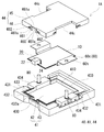
- FIG. 1 is a perspective view illustrating an outline of a substrate unit according to Embodiment 1.
- FIG. 2 is an exploded perspective view showing an outline of a substrate unit according to Embodiment 1.
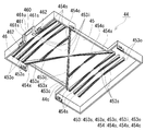
- FIG. 3 is a perspective view illustrating an outline of a lower surface of an upper cover provided in the substrate unit according to Embodiment 1.
- FIG. 3 is a bottom view illustrating an outline of a lower surface of an upper cover provided in the substrate unit according to the first embodiment.
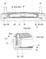
- FIG. 2 is a cross-sectional view showing a state in which the substrate unit shown in FIG. 1 is cut along a (V)-(V) cutting line. It is a perspective view which shows the outline of the waterproof wall part and inner wall part of the lower case with which the board
- an object of the present invention is to provide a board unit that can suppress the adhesion of water droplets to an internal circuit board with a simple configuration.
- the board unit of this indication can control adhesion of a water drop to an internal circuit board by simple composition.
- a substrate unit includes: A circuit board; A connector portion mounted on the circuit board; A board unit comprising a case for housing the circuit board,
- the case is A lower case having an accommodating part that opens upward and accommodates the circuit board;
- An upper cover that covers the storage portion of the lower case;
- the connector part is provided with an opening that is open to the side wall of the case so that the connector part can be fitted with the mating connector part,
- the upper cover is A ceiling portion having a board facing area facing the circuit board housed in the housing section, and an outer area located outside the board facing area without facing the circuit board; And a guide groove that is inclined from the substrate facing region to the outer region and guides water droplets present in the substrate facing region to the outer region and discharges them to the outside of the circuit board.
- the upper cover includes the guide groove.
- the water droplets adhering to the substrate facing area on the back surface (lower surface) of the upper cover can be guided to the outside area by the guide groove and discharged to the outside of the circuit board, and the water droplet can be prevented from dropping onto the circuit board. Therefore, a waterproof member such as a waterproof ring may not be provided separately. Thereby, the number of parts can be reduced, and the assembly workability of the board unit can be improved.
- the water droplets present in the substrate facing region are considered to be (1) water droplets that have entered the interior from the outside of the case (intrusion water) and (2) water droplets (condensation water) that are formed by condensation of water vapor inside the case.
- the intrusion water or dew condensation water enters the guide groove along the lower surface of the upper cover, is guided to the outer region, and is discharged to the outside of the circuit board.
- the board facing area has a connector facing area facing the connector portion, and the guide groove is formed from the connector facing area to the outer area.
- water droplets existing in the substrate facing region are often water droplets that have entered the interior from an opening formed in the side wall of the case, as compared to water droplets that have condensed. Therefore, by forming a guide groove in the connector facing area close to the opening (water droplet inlet), it is possible to guide the infiltrated water droplet to the outer area near the opening, and the back of the water drop case (board facing) This is because it is easy to prevent entry into the region.
- the ceiling portion is formed from the connector facing region to the outer region, and has an inclined rib whose height increases from the connector facing region toward the outer region,
- the guide groove is formed on an end surface of the rib.
- the lower case is A waterproof wall formed on the outer periphery of the storage part in the lower case to prevent water from entering the storage part from the outside of the case; An inner wall portion formed at an interval from the waterproof wall portion between the waterproof wall portion and the storage portion; The water droplet discharge port in the guide groove is provided so as to face between the waterproof wall portion and the inner wall portion,
- the waterproof wall portion includes a discharge portion that discharges the water droplet discharged between the waterproof wall portion and the waterproof wall portion.
- the water droplets discharged between the waterproof wall portion and the inner wall portion by the inner wall portion inside the waterproof wall portion can be prevented from flowing and adhering to the circuit board. Further, by providing the discharge portion, water droplets discharged between the waterproof wall portion and the inner wall portion can be discharged outside the waterproof wall portion without staying on the spot.
- Embodiment 1 [Board unit]
- the board unit 1 ⁇ / b> A includes a circuit board 10, a connector part 20 mounted on the circuit board 10, and a case 40 that houses the circuit board 10 and the connector part 20.
- the case 40 includes a lower case 41, an upper cover 44, and an opening 48 opened on the side wall of the case 40.
- the opening portion 48 is open so that the connector portion 20 can be fitted to a mating connector portion (not shown).
- the upper cover 44 includes a guide groove 453 that allows water droplets existing on the back surface (lower surface) of the upper cover 44 to be discharged to the outside of the circuit board 10 without dropping. .
- the lower case 41 side of the case 40 is the lower side
- the upper cover 44 side is the upper side
- the direction perpendicular to the vertical direction of the case 40 is the side where the connector unit 20 is disposed. Is the front side and the opposite side is the rear side.
- the direction orthogonal to both the up-down direction and the front-rear direction is defined as the left-right direction.
- the circuit board 10 mounts an electronic component (not shown) such as a semiconductor relay or a connector portion 20 (FIG. 2).
- the circuit board 10 includes an insulating substrate and a circuit (conductor) pattern (not shown) that is formed on one surface of the circuit board 10 and electrically connected to electronic components.
- the circuit board 10 can be a printed board.
- the connector unit 20 connects a mating connector unit (not shown) to the board unit 1A.
- the connector portion 20 includes a hood-like connector housing 22 that opens outward and can be fitted to the mating connector portion, and connector terminals 24 that extend from the inside of the connector housing 22 toward the circuit board 10 (FIG. 2). .
- the connector housing 22 is shown as a column for convenience of explanation.
- the connector terminal 24 is provided through the inner wall opposite to the opening of the connector housing 22, one end portion is disposed in the connector housing 22, and the other end portion is a conductive pattern formed on the circuit board 10. They are electrically connected (FIG. 2). This electrical connection can be performed by a known method such as soldering.
- the mating connector portion is connected to in-vehicle electrical components and the like via a wire harness.
- the case 40 accommodates the circuit board 10 (FIG. 2) and the connector part 20 inside.
- the case 40 is configured by combining a lower case 41 and an upper cover 44.
- an opening 48 is opened by the lower case 41 and the upper cover 44 so that the connector portion 20 can be fitted to the mating connector portion. 1) is formed.
- the connector portion 20 is positioned with respect to the case 40 by being sandwiched between the lower case 41 and the upper cover 44.
- the upper cover 44 covers the storage part 410 (FIG. 2) of the lower case 41 (FIG. 1).
- the upper cover 44 is an integrated body composed of a ceiling portion 45 that forms the upper surface of the case 40 and a side wall portion 46 that stands up shallow from the periphery of the ceiling portion 45.
- the upper cover 44 is formed so as to cover the upper portion of the lower case 41 with the base portion 434 of the lower case 41 exposed, and has a notch 44c in a part of the outer wall.
- the notch 44c ensures a gap through which the extended portion 60c of the bus bar 60 (described later) can pass even when the upper cover 44 is fixed to the lower case 41. By this gap, the extended portion 60 c of the bus bar 60 can be placed on the upper surface of the base portion 434.
- the ceiling portion 45 includes a substrate facing region 451 (see the outer edge of the two-dot chain line) facing the circuit substrate 10 housed in the housing portion 410, and a substrate facing region 451 that does not face the circuit substrate 10. And an outer region 452 located on the outer side.
- the shape of the ceiling portion 45 is a substantially rectangular flat plate shape, and the lower surface of the ceiling portion 45 is planar.
- the lower surface of the ceiling part 45 may be an inclined surface (triangular roof type) inclined downward from the center in the left-right direction toward both left and right sides.
- the shape of the substrate facing region 451 is the same rectangle as the shape of the circuit board 10.
- the outer region 452 has a substantially rectangular frame shape surrounding the substrate facing region 451.
- region 451 has the connector opposing area
- a guide groove 453 is formed on the lower surface of the ceiling portion 45 to prevent water droplets existing on the lower surface from falling on the circuit board 10 (FIGS. 3 and 4).
- a rib 454 is provided on the lower surface of the ceiling portion 45, and the guide groove 453 is formed in series on the lower surface of the ceiling portion 45 and the end surface of the rib 454.
- the guide groove 453 guides water droplets present in the substrate facing region 451 to the outer region 452 and discharges them to the outside of the circuit board 10. Thereby, it is possible to suppress the water droplets present in the board facing region 451 from dropping and adhering to the circuit board 10.
- the water droplets present in the substrate facing region 451 are (1) water droplets that have entered the interior from the outside of the case 40 (intrusion water), (2) water droplets that have been condensed by water vapor inside the case 40 (condensation water), Can be considered.
- Intrusion Water Drops applied to the case 40 travel along the surface of the case 40, flow toward the opening 48 formed on the side wall, and enter the inside of the case 40 from between the opening 48 and the connector portion 20. There are things to do.
- the guide groove 453 is formed to be inclined from the substrate facing region 451 to the outer region 452.
- Inclined formation means that the depth decreases from the substrate facing region 451 toward the outer region 452 and the depth is uniform from the substrate facing region 451 toward the outer region 452 as in this example.
- the guide groove 453 itself is inclined with respect to the horizontal direction by an inclined rib 454 described later.
- the number of guide grooves 453 may be singular or plural.
- the guide groove 453 is preferably provided at least in the vicinity of the opening 48, for example, from the connector facing region 451a of the substrate facing region 451 to the left and right outer regions 452. If it does so, it will be easy to prevent the water droplet which infiltrated in the case 40 to fall to the circuit board 10. Since the guide groove 453 is provided near the opening 48 that is the inlet of the water droplet in the case 40, the infiltrated water droplet can be guided to the outer region 452 in the vicinity of the inlet, and the water droplet can be moved to the back of the case 40. This is because it is easy to prevent the intrusion.
- the longitudinal direction of the guide groove 453 formed from the connector facing region 451a to the left and right outer regions 452 is preferably along the left-right direction. Then, since the guide groove 453 is formed in a straight line and the length to the outer region 452 is easily shortened, water droplets are easily discharged to the outside of the circuit board 10 without falling on the circuit board 10.
- the guide grooves 453 are provided in a portion extending from the extension region 451b to the left and right outer regions 452 in addition to a portion extending from the connector facing region 451a to the left and right outer regions 452. . If it does so, it will be easy to prevent the fall to the circuit board 10 of the water droplet which water vapor
- FIG. The longitudinal direction of the guide groove 453 formed from the extension region 451b to the left and right outer regions 452 can be selected as appropriate.
- the left-right direction similar to the case where the guide groove 453 is formed from the connector facing region 451a to the outer region 452, or an oblique direction intersecting both the left-right and front-rear directions can be given.
- the guide grooves 453 are formed to be evenly distributed on the lower surface of the ceiling portion 45 so as to make it easy to prevent the condensed water droplets from falling on the circuit board 10 wherever they are present on the lower surface of the ceiling portion 45. Is preferred.
- three lateral guide grooves 453s (total of six) arranged in parallel in the front-rear direction on each of the front side and the rear side, a cross-shaped oblique guide groove 453x in the center, and an oblique guide groove
- Two connection guide grooves 453c are formed opposite to each other across the intersection of 453x.
- the foremost horizontal guide groove 453s extends in the left-right direction and extends from the center in the left-right direction of the connector facing region 451a to the left and right outer regions 452.
- the remaining five horizontal guide grooves 453s are formed from the center in the left-right direction of the extension region 451b to the left and right outer regions 452 along the left-right direction.
- the oblique guide groove 453x intersects both the left and right and front and rear directions and is formed from the approximate center of the extension region 451b to the left and right outer regions 452.
- the oblique guide groove 453x communicates with the center.
- the two connecting guide grooves 453c are formed along the left-right direction and extending from the extended region 451b to the two oblique guide grooves 453x.
- the two connection guide grooves 453c communicate with the two oblique guide grooves 453x.
- the water drop inlet 453i of each guide groove 453 is formed in the connector facing region 451a and the extended region 451b.
- Each inflow port 453i is located at the center of the guide groove 453 or at an intersecting position.
- the opening end of the water droplet inlet 453 i of each guide groove 453 is flush with the lower surface of the ceiling 45. Therefore, it is easy for water droplets to flow into the guide groove.
- the water droplet discharge port 453o of each guide groove 453 is provided so as to face between a waterproof wall portion 432 and an inner wall portion 433 of the lower case 41 described later (an enlarged view of FIG. 5). Therefore, water droplets flowing through each guide groove 453 fall between the waterproof wall portion 432 and the inner wall portion 433 and are discharged.
- the cross-sectional shape of the guide groove 453 can be selected as appropriate. here.
- the cross-sectional shape of the guide groove 453 is a semicircular shape (an enlarged view of the cross section of FIGS. 4B to 4B).
- the width of the guide groove 453 is preferably a width at which capillary action occurs. Due to the capillary phenomenon in which the guide groove 453 is regarded as a capillary, water droplets existing in the substrate facing region 451 can be easily guided to the outer region 452 along the guide groove 453. As the width of the guide groove 453 is narrower, the effect of capillary action can be obtained. However, it is preferable that the width of the guide groove 453 is not excessively narrow.
- the depth of the guide groove 453 can be appropriately selected according to the location where the guide groove 453 is formed. When formed on the end face of the rib 454 as in this example, the depth of the guide groove 453 may be uniform in the longitudinal direction.
- -Rib Rib 454 reinforces ceiling part 45.
- the rib 454 is used in a part of the guide groove 453 where it is formed. The greater the number of ribs 454, the higher the strength of the ceiling 45.
- the rib 454 may be provided from the substrate facing region 451 to the outer region 452 in consideration of the use of the rib 454 as a formation location of the guide groove 453. This is because the guide groove 453 can be provided from the substrate facing region 451 to the outer region 452. More specifically, it may be provided from the connector facing region 451a or the extension region 451b of the substrate facing region 451 to the outer region 452.
- the guide groove 453 can be provided from the connector facing region 451a to the outer region 452. Therefore, it is easy to prevent water droplets that have entered the case 40 from falling onto the circuit board 10.
- the longitudinal direction of the rib 454 formed from the connector facing region 451a to the outer region 452 is preferably the left-right direction.
- the guide groove 453 can be provided from the extended region 451b to the outer region 452. Therefore, it is easy to prevent the water droplets in which the water vapor is condensed in the case 40 from dropping onto the circuit board 10.
- the longitudinal direction of the rib 454 formed from the extended region 451b to the outer region 452 may be a left-right direction or an oblique direction.
- ribs 454 that are connected to each other may be provided.
- the guide grooves 453 formed on the end faces of the ribs 454 to be connected may communicate with each other.
- the ceiling portion 45 there are three pairs of horizontal ribs 454s (6 pairs in total) juxtaposed in the front-rear direction on each of the front side and the rear side, and four diagonal ribs 454x arranged in a cross shape at substantially the center. And two pairs of connecting ribs 454c that are opposed to each other across the center and are connected to the oblique ribs 454x.
- Each pair of horizontal ribs 454s is provided along the left-right direction and spaced apart from each other on the same straight line.
- the foremost pair of horizontal ribs 454s is formed from the vicinity of the left and right ends of the connector facing region 451a to the outer regions 452 on the left and right sides.
- the remaining five pairs of horizontal ribs 454s are formed from the vicinity of the left and right end portions of the extension region 451b to the outer regions 452 on both the left and right sides.
- a series of lateral guide grooves 453 s are formed on the lower surface of the ceiling portion 45 between each pair of lateral ribs 454 s and on the end surfaces of each pair of lateral ribs 454 s.
- the four diagonal ribs 454x are two along each of one diagonal direction and the other diagonal direction of two intersecting diagonal directions, and are provided at intervals on the same diagonal line.
- the four oblique ribs 454x are formed from the vicinity of the left and right end portions of the extension region 451b to the left and right outer regions 452 so as to intersect both the left and right and front and rear directions.
- a series of oblique guide grooves 453x are formed on the lower surface of the ceiling portion 45 between the two oblique ribs 454x located on the same diagonal line and the end faces of the two oblique ribs 454x.
- Each pair of connecting ribs 454c is provided along the left-right direction and spaced apart from each other on the same straight line. Each pair of connecting ribs 454c is formed from the vicinity of the left and right ends of the extension region 451b to the oblique ribs 454x. A series of connection guide grooves 453c are formed on the lower surface of the ceiling portion 45 between each pair of connection ribs 454c and the end surfaces of each pair of connection ribs 454c.
- Each of the ribs 454 has an inclined shape (triangular shape) whose height increases from the connector facing region 451a or the extended region 451b toward the outer region 452.
- One end (the inlet 453i side) of each rib 454 is provided in the vicinity of the left and right ends of the connector facing region 451a and the extension region 451b. Accordingly, each rib 454 does not hinder the inflow of water droplets into the guide groove 453, and the water droplets can easily flow into the guide groove 453.
- the other end (exhaust port 453 o side) of each rib 454 is provided in the outer region 452.
- the outlet 453o of the guide groove 453 formed on the end face of the rib 454 is provided in the outer region 452. Therefore, it is easy to flow the water droplet to the outer region 452 and to prevent the water droplet from dropping onto the circuit board 10.
- the side wall portion 46 engages with the lower case 41 to integrate the upper cover 44 and the lower case 41. This prevents water from entering the inside of the case 40 from the outside.
- the location where the side wall 46 is formed is a location excluding the central portions on the left and right sides of the periphery of the ceiling 45. That is, the side wall 43 is formed in series on the front periphery of the ceiling 45 and the front periphery on both left and right sides, and is formed in series on the rear periphery on the ceiling 45 and the rear periphery on both sides. ing.
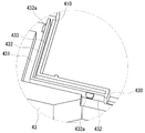
- the side wall portion 46 is inserted into an insertion groove 431 (FIGS. 2, 5, and 6) formed on the upper surface of the lower case 41.
- the side wall portion 46 includes an upper concave portion 460, a protruding portion 461, and an engagement hole 462.
- the upper recessed part 460 forms the opening part 48 by which the connector part 20 is arrange
- the upper concave portion 460 is formed at a location corresponding to the lower concave portion 430 and a central portion of the side wall portion 46 on the front side.
- the size of the upper concave portion 460 can be selected as appropriate so that the connector portion 20 can be disposed in the opening 48 formed by the lower concave portion 430 and can be positioned with respect to the case 40 of the connector portion 20.
- the upper concave portion 460 is disposed so that the distal end side of the connector portion 20 is exposed outward.
- the protrusion part 461 is formed in the circumference
- the upper portion 461u of the protruding portion 461 is formed as a flat surface substantially flush with the surface (upper surface) of the ceiling portion 45.
- the engagement hole 462 engages with the engagement protrusion 432a of the lower case 41 (waterproof wall part 432). By this engagement, the insertion state of the side wall portion 46 into the insertion groove 431 is maintained, whereby the upper cover 44 and the lower case 41 are fixed.
- the positions where the engagement holes 462 are formed are provided at appropriate positions in the circumferential direction of the side wall portion 46, and here, the front side wall portion 46 and the left and right side wall portions 46 are provided.
- Examples of the material of the upper cover 44 include synthetic resins such as polypropylene (PP) resin and polyamide (PA) resin.
- the lower case 41 accommodates the circuit board 10, the connector part 20, and a bus bar 60 (described later) inside (FIG. 2).
- the lower case 41 is composed of a bottom portion 42 and a side wall portion 43 erected shallowly from the periphery of the bottom portion 42, and has a box shape having an opening on the opposite side (upper side) from the bottom portion 42.
- a storage portion 410 that stores the circuit board 10, the connector portion 20, and the bus bar 60 is formed at a location surrounded by the bottom portion 42 and the side wall portion 43.
- the bottom part 42 and the side wall part 43 are not integrally molded, but are independent members, and are integrated by a fixing member such as a screw 42b (FIG. 5).
- the bottom part 42 and the side wall part 43 may be integrally molded.
- the shape of the bottom portion 42 is a flat plate shape larger than the circuit board 10 and the bus bar 60.
- the bottom portion 42 is formed with an insertion hole (not shown) through which a screw 42 b integrated with the side wall portion 43 is inserted.
- the bottom portion 42 is configured by a heat sink that dissipates heat of the electronic component mounted on the circuit board 10.
- a metal plate such as aluminum can be used.
- the side wall portion 43 forms a storage portion 410 that stores the circuit board 10 and the bus bar 60 together with the bottom portion 42 (FIG. 2).
- the shape of the side wall portion 43 is a substantially rectangular frame that is continuous over the entire circumference of the bottom portion 42, and the side wall portion 43 surrounds four sides of the outer periphery of the circuit board 10 including the connector portion 20.
- the side wall portion 43 includes a lower concave portion 430 formed on the upper surface thereof, an insertion groove 431, a waterproof wall portion 432, an inner wall portion 433, a base portion 434, and a step portion 435 (FIG. 5) formed on the lower surface thereof. Have.
- the lower recessed part 430 forms the opening part 48 (FIG. 1) by which the connector part 20 is arrange
- the formation part of the lower side recessed part 430 is a part corresponding to the upper side recessed part 460, and is a center part of the side wall part 43 of the front.
- the size of the lower concave portion 430 can be appropriately selected as the connector portion 20 can be disposed in the opening 48 formed by the upper concave portion 460 and can be positioned with respect to the case 40 of the connector portion 20.
- the side wall part 46 of the upper cover 44 is inserted (FIG. 2, FIG. 6).
- the formation location (shape viewed from above) of the insertion groove 431 can be appropriately selected according to the location (shape viewed from the bottom surface) of the side wall portion 46 of the upper cover 44.
- the insertion groove 431 is formed at a location excluding the left and right central portions on the upper surface of the side wall portion 43.
- the insertion grooves 431 are formed in the left and right corners of the front side wall 43 and the left and right regions on the rear side.
- the shape of the front insertion groove 431 in plan view is L-shaped, and the shape of the rear insertion groove 431 in plan view is I-shaped.
- the width and depth of the insertion groove 431 can be appropriately selected according to the thickness of the side wall portion 46 of the upper cover 44 and the insertion amount.
- the waterproof wall part 432 is formed in the outer periphery of the accommodating part 410, and prevents permeation of the water into the accommodating part 410 from the exterior of the case 40 (FIG. 2, FIG. 6).
- the waterproof wall portion 432 forms a side surface of the insertion groove 431 and is provided between the side wall portion 46 of the upper cover 44 and the storage portion 410 when the upper cover 44 is inserted into the insertion groove 431. It contacts with the inner surface of the side wall 46 of 44.
- the location where the waterproof wall 432 is formed is the same as that of the insertion groove 431, and is the left and right corners of the front side wall 43 and the left and right regions on the rear side.
- the shape of the front waterproof wall 432 in plan view is L-shaped, and the shape of the rear waterproof wall 432 in plan view is I-shaped.
- the waterproof wall portion 432 includes an engagement protrusion 432a and a drainage portion (not shown).
- the engagement protrusion 432a engages with the engagement hole 462 of the side wall portion 46 of the upper cover 44 inserted into the insertion groove 431 (FIGS. 2 and 6). By this engagement, the upper cover 44 and the lower case 41 are fixed.
- the formation position of the engagement protrusion 423 is a position corresponding to the engagement hole 462, provided at an appropriate position in the circumferential direction of the side wall 43, and provided on the front waterproof wall 432 and the left and right waterproof wall 432. .
- the drainage part discharges water droplets discharged between the inner wall part 433 and the waterproof wall part 432.
- the inner wall part 433 prevents the water droplet discharged
- the inner wall portion 433 is formed between the waterproof wall portion 432 and the storage portion 410 with a space from the waterproof wall portion 432.
- the inner wall portion 433 forms an edge of the storage portion 410.
- the location where the inner wall 433 is formed is the same as that of the waterproof wall 432 and is a region extending from the left and right corners of the front side wall 43 and from the left corner to the right corner on the rear side.
- the shape of the front inner wall portion 433 in plan view is L-shaped, and the shape of the rear inner wall portion 433 in plan view is [letter shape.
- the base part 434 has a terminal fixing
- the base part 434 is formed on the upper surface of the central part on both the left and right sides.
- the extended portion 60 c of the bus bar 60 is placed on the base portion 434.
- the bottom part 42 is engage
- the step portion 435 is formed on the inner peripheral edge portion of the lower surface of the side wall portion 43.
- the stepped portion 435 is formed with a screw hole (not shown) for fixing the screw 42b integrated with the bottom portion 42.
- the material of the lower case 41 is, for example, a synthetic resin such as PP resin or PA resin, similar to the upper cover 44.
- the bus bar 60 constitutes a power circuit.
- the bus bar 60 is connected to a power source or an electrical load.
- the bus bar 60 includes a central portion and extending portions 60c that extend stepwise on the left and right sides thereof.
- a front portion of the central portion of the bus bar 60 is located below the connector portion 20 and is interposed between the lower surface of the circuit board 10 and the upper surface of the bottom portion 42.
- the central portion and the extending portion 60c are integrally formed.
- the central portion is formed in a planar shape and is interposed between the lower surface of the circuit board 10 and the upper surface of the bottom portion 42.
- the extending portion 60 c is disposed on the upper surface of the base portion 434 of the lower case 41.
- the extending portion 60c is formed to be bent in a step shape, and is continuous on both sides of the central portion.
- the extended portion 60c is a portion for electrically connecting an external device, and a connection terminal of an electric wire (wire harness) (not shown) is electrically connected thereto.
- a terminal insertion hole 60h through which the male screw portion 80 is inserted is formed in the extended portion 60c.
- the male screw part 80 fixed to the terminal fixing part of the lower case 41 is inserted into the terminal insertion hole 60h.
- a wire harness (not shown) is attached to the male screw portion 80.
- the bus bar 60 and the wire harness are electrically connected via the male screw portion 80. Examples of the material of the bus bar 60 include a conductive metal, and specifically copper or a copper alloy.
- an adhesive sheet (not shown) interposed between the both 10 and 60 can be used.
- the substrate unit 1A can be suitably used for a substrate unit disposed in a location where waterproofing is not required in an automobile.
- the substrate unit 1A can be suitably used for a large current power control unit such as a DC voltage converter, an AC / DC converter, and a DC / AC inverter.
- a waterproof member such as a waterproof ring is not separately provided, but an inclined rib 454 is formed on the lower surface of the ceiling portion 45 of the upper cover 44, and a guide groove 453 is formed on an end surface thereof.
- the substrate unit 1A can ensure the drip-proof property without separately providing a waterproof member. Therefore, it can be suitably used to ensure waterproofing (drip-proofing) of water drops. Moreover, since it is not necessary to provide a waterproof member separately, the number of parts can be reduced and the assembly workability of the board unit 1A can be improved.
- ⁇ Modification 1 In the substrate unit of the first modification, the ribs are not provided, and the guide groove can be directly formed on the lower surface (back surface) of the ceiling portion instead of the end surface of the rib.
- the depth of the guide groove is preferably shallower from the board facing area (connector facing area or extension area) toward the outer area. If it does so, the water droplet which exists in a board
- the lower surface of the ceiling portion can be an inclined surface (triangular roof type) that is inclined downward from the center in the left-right direction toward both left and right sides.
- the depth of the guide groove and the height of the rib can be made uniform in the longitudinal direction.
Landscapes
- Engineering & Computer Science (AREA)
- Microelectronics & Electronic Packaging (AREA)
- Casings For Electric Apparatus (AREA)
Priority Applications (3)
| Application Number | Priority Date | Filing Date | Title |
|---|---|---|---|
| CN201780032848.4A CN109315073B (zh) | 2016-06-08 | 2017-06-06 | 基板单元 |
| US16/306,940 US10653019B2 (en) | 2016-06-08 | 2017-06-06 | Substrate unit |
| DE112017002906.6T DE112017002906T5 (de) | 2016-06-08 | 2017-06-06 | Substrateinheit |
Applications Claiming Priority (2)
| Application Number | Priority Date | Filing Date | Title |
|---|---|---|---|
| JP2016-114857 | 2016-06-08 | ||
| JP2016114857A JP6604519B2 (ja) | 2016-06-08 | 2016-06-08 | 基板ユニット |
Publications (1)
| Publication Number | Publication Date |
|---|---|
| WO2017213144A1 true WO2017213144A1 (ja) | 2017-12-14 |
Family
ID=60577849
Family Applications (1)
| Application Number | Title | Priority Date | Filing Date |
|---|---|---|---|
| PCT/JP2017/021002 Ceased WO2017213144A1 (ja) | 2016-06-08 | 2017-06-06 | 基板ユニット |
Country Status (5)
| Country | Link |
|---|---|
| US (1) | US10653019B2 (enExample) |
| JP (1) | JP6604519B2 (enExample) |
| CN (1) | CN109315073B (enExample) |
| DE (1) | DE112017002906T5 (enExample) |
| WO (1) | WO2017213144A1 (enExample) |
Families Citing this family (4)
| Publication number | Priority date | Publication date | Assignee | Title |
|---|---|---|---|---|
| JP6632038B2 (ja) | 2018-01-31 | 2020-01-15 | Necプラットフォームズ株式会社 | 放熱耐水構造 |
| JP2019149520A (ja) | 2018-02-28 | 2019-09-05 | ファナック株式会社 | 電子機器 |
| JP7307669B2 (ja) * | 2019-12-16 | 2023-07-12 | 日立Astemo株式会社 | 電力変換装置 |
| JP7615717B2 (ja) * | 2021-02-04 | 2025-01-17 | 住友電装株式会社 | 電気接続箱 |
Citations (8)
| Publication number | Priority date | Publication date | Assignee | Title |
|---|---|---|---|---|
| JP2001118628A (ja) * | 1999-10-21 | 2001-04-27 | Sumitomo Wiring Syst Ltd | コネクタ |
| JP2002335090A (ja) * | 2001-05-07 | 2002-11-22 | Denso Corp | 電子機器 |
| JP2003229678A (ja) * | 2002-01-31 | 2003-08-15 | Denso Corp | 電子制御装置の筐体構造 |
| JP2004096968A (ja) * | 2002-09-04 | 2004-03-25 | Sumitomo Wiring Syst Ltd | 電気接続箱の排水構造 |
| JP2006050814A (ja) * | 2004-08-05 | 2006-02-16 | Auto Network Gijutsu Kenkyusho:Kk | 電気接続箱 |
| JP2006344687A (ja) * | 2005-06-07 | 2006-12-21 | Denso Corp | 電子装置用筐体 |
| JP2011229253A (ja) * | 2010-04-19 | 2011-11-10 | Yazaki Corp | 電気接続箱 |
| WO2016158445A1 (ja) * | 2015-03-27 | 2016-10-06 | 日本電気株式会社 | 電子機器の蓋部材及び電子機器の筐体 |
Family Cites Families (4)
| Publication number | Priority date | Publication date | Assignee | Title |
|---|---|---|---|---|
| CN103858289B (zh) * | 2011-10-05 | 2017-01-18 | 株式会社自动网络技术研究所 | 能够外部连接的电子电路单元 |
| JP2014175365A (ja) | 2013-03-06 | 2014-09-22 | Aisin Kiko Co Ltd | 基板ケース |
| JP2016114857A (ja) | 2014-12-16 | 2016-06-23 | キヤノン株式会社 | 情報処理装置、その制御方法、プログラム、及び記憶媒体 |
| JP2016186979A (ja) * | 2015-03-27 | 2016-10-27 | 日本電気株式会社 | 電子機器の蓋部材及び電子機器の筐体 |
-
2016
- 2016-06-08 JP JP2016114857A patent/JP6604519B2/ja not_active Expired - Fee Related
-
2017
- 2017-06-06 US US16/306,940 patent/US10653019B2/en active Active
- 2017-06-06 DE DE112017002906.6T patent/DE112017002906T5/de not_active Ceased
- 2017-06-06 CN CN201780032848.4A patent/CN109315073B/zh not_active Expired - Fee Related
- 2017-06-06 WO PCT/JP2017/021002 patent/WO2017213144A1/ja not_active Ceased
Patent Citations (8)
| Publication number | Priority date | Publication date | Assignee | Title |
|---|---|---|---|---|
| JP2001118628A (ja) * | 1999-10-21 | 2001-04-27 | Sumitomo Wiring Syst Ltd | コネクタ |
| JP2002335090A (ja) * | 2001-05-07 | 2002-11-22 | Denso Corp | 電子機器 |
| JP2003229678A (ja) * | 2002-01-31 | 2003-08-15 | Denso Corp | 電子制御装置の筐体構造 |
| JP2004096968A (ja) * | 2002-09-04 | 2004-03-25 | Sumitomo Wiring Syst Ltd | 電気接続箱の排水構造 |
| JP2006050814A (ja) * | 2004-08-05 | 2006-02-16 | Auto Network Gijutsu Kenkyusho:Kk | 電気接続箱 |
| JP2006344687A (ja) * | 2005-06-07 | 2006-12-21 | Denso Corp | 電子装置用筐体 |
| JP2011229253A (ja) * | 2010-04-19 | 2011-11-10 | Yazaki Corp | 電気接続箱 |
| WO2016158445A1 (ja) * | 2015-03-27 | 2016-10-06 | 日本電気株式会社 | 電子機器の蓋部材及び電子機器の筐体 |
Also Published As
| Publication number | Publication date |
|---|---|
| JP2017220597A (ja) | 2017-12-14 |
| CN109315073A (zh) | 2019-02-05 |
| DE112017002906T5 (de) | 2019-02-21 |
| JP6604519B2 (ja) | 2019-11-13 |
| CN109315073B (zh) | 2020-08-25 |
| US10653019B2 (en) | 2020-05-12 |
| US20190150303A1 (en) | 2019-05-16 |
Similar Documents
| Publication | Publication Date | Title |
|---|---|---|
| JP5173596B2 (ja) | 電気接続箱 | |
| US8389856B2 (en) | Waterproof structure of electrical junction box | |
| US7931478B2 (en) | Electrical junction box | |
| JP6604519B2 (ja) | 基板ユニット | |
| JP5051465B2 (ja) | 電気接続箱 | |
| US7841869B2 (en) | Connector for board and electrical junction box | |
| CN109196965B (zh) | 基板单元 | |
| CN109076712B (zh) | 基板单元 | |
| JP4657025B2 (ja) | 電気接続箱 | |
| JP6318085B2 (ja) | 電気接続箱の排水構造 | |
| US11147173B2 (en) | Electronic device | |
| US20060292903A1 (en) | Electric connection box | |
| JP5471793B2 (ja) | 電気接続箱 | |
| JP2000092652A (ja) | 電気接続箱 | |
| JP4374296B2 (ja) | 電気接続箱 | |
| JP2006050814A (ja) | 電気接続箱 | |
| JP2007259652A (ja) | 電気接続箱 | |
| JP6287888B2 (ja) | ケース | |
| JP5733164B2 (ja) | 回路ユニット | |
| JP2013206952A (ja) | 電子装置 | |
| CN104685742A (zh) | 电连接箱 | |
| JP2007110852A (ja) | 電気接続箱 |
Legal Events
| Date | Code | Title | Description |
|---|---|---|---|
| 121 | Ep: the epo has been informed by wipo that ep was designated in this application |
Ref document number: 17810319 Country of ref document: EP Kind code of ref document: A1 |
|
| 122 | Ep: pct application non-entry in european phase |
Ref document number: 17810319 Country of ref document: EP Kind code of ref document: A1 |