WO2017208668A1 - 半導体素子の駆動装置 - Google Patents
半導体素子の駆動装置 Download PDFInfo
- Publication number
- WO2017208668A1 WO2017208668A1 PCT/JP2017/015987 JP2017015987W WO2017208668A1 WO 2017208668 A1 WO2017208668 A1 WO 2017208668A1 JP 2017015987 W JP2017015987 W JP 2017015987W WO 2017208668 A1 WO2017208668 A1 WO 2017208668A1
- Authority
- WO
- WIPO (PCT)
- Prior art keywords
- signal
- protection
- level
- output
- input
- Prior art date
- Legal status (The legal status is an assumption and is not a legal conclusion. Google has not performed a legal analysis and makes no representation as to the accuracy of the status listed.)
- Ceased
Links
Images

Classifications
-
- H—ELECTRICITY
- H02—GENERATION; CONVERSION OR DISTRIBUTION OF ELECTRIC POWER
- H02H—EMERGENCY PROTECTIVE CIRCUIT ARRANGEMENTS
- H02H7/00—Emergency protective circuit arrangements specially adapted for specific types of electric machines or apparatus or for sectionalised protection of cable or line systems, and effecting automatic switching in the event of an undesired change from normal working conditions
- H02H7/10—Emergency protective circuit arrangements specially adapted for specific types of electric machines or apparatus or for sectionalised protection of cable or line systems, and effecting automatic switching in the event of an undesired change from normal working conditions for converters; for rectifiers
- H02H7/12—Emergency protective circuit arrangements specially adapted for specific types of electric machines or apparatus or for sectionalised protection of cable or line systems, and effecting automatic switching in the event of an undesired change from normal working conditions for converters; for rectifiers for static converters or rectifiers
- H02H7/122—Emergency protective circuit arrangements specially adapted for specific types of electric machines or apparatus or for sectionalised protection of cable or line systems, and effecting automatic switching in the event of an undesired change from normal working conditions for converters; for rectifiers for static converters or rectifiers for inverters, i.e. DC/AC converters
-
- G—PHYSICS
- G01—MEASURING; TESTING
- G01R—MEASURING ELECTRIC VARIABLES; MEASURING MAGNETIC VARIABLES
- G01R19/00—Arrangements for measuring currents or voltages or for indicating presence or sign thereof
- G01R19/165—Indicating that current or voltage is either above or below a predetermined value or within or outside a predetermined range of values
- G01R19/16533—Indicating that current or voltage is either above or below a predetermined value or within or outside a predetermined range of values characterised by the application
- G01R19/16538—Indicating that current or voltage is either above or below a predetermined value or within or outside a predetermined range of values characterised by the application in AC or DC supplies
- G01R19/16547—Indicating that current or voltage is either above or below a predetermined value or within or outside a predetermined range of values characterised by the application in AC or DC supplies voltage or current in AC supplies
-
- G—PHYSICS
- G01—MEASURING; TESTING
- G01R—MEASURING ELECTRIC VARIABLES; MEASURING MAGNETIC VARIABLES
- G01R31/00—Arrangements for testing electric properties; Arrangements for locating electric faults; Arrangements for electrical testing characterised by what is being tested not provided for elsewhere
- G01R31/26—Testing of individual semiconductor devices
- G01R31/2607—Circuits therefor
- G01R31/2608—Circuits therefor for testing bipolar transistors
- G01R31/2619—Circuits therefor for testing bipolar transistors for measuring thermal properties thereof
-
- G—PHYSICS
- G01—MEASURING; TESTING
- G01R—MEASURING ELECTRIC VARIABLES; MEASURING MAGNETIC VARIABLES
- G01R31/00—Arrangements for testing electric properties; Arrangements for locating electric faults; Arrangements for electrical testing characterised by what is being tested not provided for elsewhere
- G01R31/40—Testing power supplies
- G01R31/42—AC power supplies
-
- H—ELECTRICITY
- H02—GENERATION; CONVERSION OR DISTRIBUTION OF ELECTRIC POWER
- H02H—EMERGENCY PROTECTIVE CIRCUIT ARRANGEMENTS
- H02H1/00—Details of emergency protective circuit arrangements
- H02H1/0007—Details of emergency protective circuit arrangements concerning the detecting means
-
- H—ELECTRICITY
- H02—GENERATION; CONVERSION OR DISTRIBUTION OF ELECTRIC POWER
- H02H—EMERGENCY PROTECTIVE CIRCUIT ARRANGEMENTS
- H02H1/00—Details of emergency protective circuit arrangements
- H02H1/0061—Details of emergency protective circuit arrangements concerning transmission of signals
-
- H—ELECTRICITY
- H02—GENERATION; CONVERSION OR DISTRIBUTION OF ELECTRIC POWER
- H02H—EMERGENCY PROTECTIVE CIRCUIT ARRANGEMENTS
- H02H7/00—Emergency protective circuit arrangements specially adapted for specific types of electric machines or apparatus or for sectionalised protection of cable or line systems, and effecting automatic switching in the event of an undesired change from normal working conditions
- H02H7/22—Emergency protective circuit arrangements specially adapted for specific types of electric machines or apparatus or for sectionalised protection of cable or line systems, and effecting automatic switching in the event of an undesired change from normal working conditions for distribution gear, e.g. bus-bar systems; for switching devices
- H02H7/222—Emergency protective circuit arrangements specially adapted for specific types of electric machines or apparatus or for sectionalised protection of cable or line systems, and effecting automatic switching in the event of an undesired change from normal working conditions for distribution gear, e.g. bus-bar systems; for switching devices for switches
-
- H—ELECTRICITY
- H02—GENERATION; CONVERSION OR DISTRIBUTION OF ELECTRIC POWER
- H02M—APPARATUS FOR CONVERSION BETWEEN AC AND AC, BETWEEN AC AND DC, OR BETWEEN DC AND DC, AND FOR USE WITH MAINS OR SIMILAR POWER SUPPLY SYSTEMS; CONVERSION OF DC OR AC INPUT POWER INTO SURGE OUTPUT POWER; CONTROL OR REGULATION THEREOF
- H02M1/00—Details of apparatus for conversion
- H02M1/08—Circuits specially adapted for the generation of control voltages for semiconductor devices incorporated in static converters
-
- H—ELECTRICITY
- H02—GENERATION; CONVERSION OR DISTRIBUTION OF ELECTRIC POWER
- H02M—APPARATUS FOR CONVERSION BETWEEN AC AND AC, BETWEEN AC AND DC, OR BETWEEN DC AND DC, AND FOR USE WITH MAINS OR SIMILAR POWER SUPPLY SYSTEMS; CONVERSION OF DC OR AC INPUT POWER INTO SURGE OUTPUT POWER; CONTROL OR REGULATION THEREOF
- H02M1/00—Details of apparatus for conversion
- H02M1/32—Means for protecting converters other than automatic disconnection
-
- H—ELECTRICITY
- H02—GENERATION; CONVERSION OR DISTRIBUTION OF ELECTRIC POWER
- H02M—APPARATUS FOR CONVERSION BETWEEN AC AND AC, BETWEEN AC AND DC, OR BETWEEN DC AND DC, AND FOR USE WITH MAINS OR SIMILAR POWER SUPPLY SYSTEMS; CONVERSION OF DC OR AC INPUT POWER INTO SURGE OUTPUT POWER; CONTROL OR REGULATION THEREOF
- H02M7/00—Conversion of AC power input into DC power output; Conversion of DC power input into AC power output
- H02M7/42—Conversion of DC power input into AC power output without possibility of reversal
- H02M7/44—Conversion of DC power input into AC power output without possibility of reversal by static converters
- H02M7/48—Conversion of DC power input into AC power output without possibility of reversal by static converters using discharge tubes with control electrode or semiconductor devices with control electrode
- H02M7/53—Conversion of DC power input into AC power output without possibility of reversal by static converters using discharge tubes with control electrode or semiconductor devices with control electrode using devices of a triode or transistor type requiring continuous application of a control signal
- H02M7/537—Conversion of DC power input into AC power output without possibility of reversal by static converters using discharge tubes with control electrode or semiconductor devices with control electrode using devices of a triode or transistor type requiring continuous application of a control signal using semiconductor devices only, e.g. single switched pulse inverters
- H02M7/5387—Conversion of DC power input into AC power output without possibility of reversal by static converters using discharge tubes with control electrode or semiconductor devices with control electrode using devices of a triode or transistor type requiring continuous application of a control signal using semiconductor devices only, e.g. single switched pulse inverters in a bridge configuration
-
- H—ELECTRICITY
- H02—GENERATION; CONVERSION OR DISTRIBUTION OF ELECTRIC POWER
- H02M—APPARATUS FOR CONVERSION BETWEEN AC AND AC, BETWEEN AC AND DC, OR BETWEEN DC AND DC, AND FOR USE WITH MAINS OR SIMILAR POWER SUPPLY SYSTEMS; CONVERSION OF DC OR AC INPUT POWER INTO SURGE OUTPUT POWER; CONTROL OR REGULATION THEREOF
- H02M7/00—Conversion of AC power input into DC power output; Conversion of DC power input into AC power output
- H02M7/42—Conversion of DC power input into AC power output without possibility of reversal
- H02M7/44—Conversion of DC power input into AC power output without possibility of reversal by static converters
- H02M7/48—Conversion of DC power input into AC power output without possibility of reversal by static converters using discharge tubes with control electrode or semiconductor devices with control electrode
- H02M7/53—Conversion of DC power input into AC power output without possibility of reversal by static converters using discharge tubes with control electrode or semiconductor devices with control electrode using devices of a triode or transistor type requiring continuous application of a control signal
- H02M7/537—Conversion of DC power input into AC power output without possibility of reversal by static converters using discharge tubes with control electrode or semiconductor devices with control electrode using devices of a triode or transistor type requiring continuous application of a control signal using semiconductor devices only, e.g. single switched pulse inverters
- H02M7/5387—Conversion of DC power input into AC power output without possibility of reversal by static converters using discharge tubes with control electrode or semiconductor devices with control electrode using devices of a triode or transistor type requiring continuous application of a control signal using semiconductor devices only, e.g. single switched pulse inverters in a bridge configuration
- H02M7/53871—Conversion of DC power input into AC power output without possibility of reversal by static converters using discharge tubes with control electrode or semiconductor devices with control electrode using devices of a triode or transistor type requiring continuous application of a control signal using semiconductor devices only, e.g. single switched pulse inverters in a bridge configuration with automatic control of output voltage or current
-
- H—ELECTRICITY
- H03—ELECTRONIC CIRCUITRY
- H03K—PULSE TECHNIQUE
- H03K17/00—Electronic switching or gating, i.e. not by contact-making and –breaking
- H03K17/08—Modifications for protecting switching circuit against overcurrent or overvoltage
- H03K17/081—Modifications for protecting switching circuit against overcurrent or overvoltage without feedback from the output circuit to the control circuit
- H03K17/0812—Modifications for protecting switching circuit against overcurrent or overvoltage without feedback from the output circuit to the control circuit by measures taken in the control circuit
- H03K17/08128—Modifications for protecting switching circuit against overcurrent or overvoltage without feedback from the output circuit to the control circuit by measures taken in the control circuit in composite switches
-
- H—ELECTRICITY
- H03—ELECTRONIC CIRCUITRY
- H03K—PULSE TECHNIQUE
- H03K17/00—Electronic switching or gating, i.e. not by contact-making and –breaking
- H03K17/08—Modifications for protecting switching circuit against overcurrent or overvoltage
- H03K17/082—Modifications for protecting switching circuit against overcurrent or overvoltage by feedback from the output to the control circuit
- H03K17/0828—Modifications for protecting switching circuit against overcurrent or overvoltage by feedback from the output to the control circuit in composite switches
-
- H—ELECTRICITY
- H03—ELECTRONIC CIRCUITRY
- H03K—PULSE TECHNIQUE
- H03K17/00—Electronic switching or gating, i.e. not by contact-making and –breaking
- H03K17/18—Modifications for indicating state of switch
-
- H—ELECTRICITY
- H02—GENERATION; CONVERSION OR DISTRIBUTION OF ELECTRIC POWER
- H02M—APPARATUS FOR CONVERSION BETWEEN AC AND AC, BETWEEN AC AND DC, OR BETWEEN DC AND DC, AND FOR USE WITH MAINS OR SIMILAR POWER SUPPLY SYSTEMS; CONVERSION OF DC OR AC INPUT POWER INTO SURGE OUTPUT POWER; CONTROL OR REGULATION THEREOF
- H02M1/00—Details of apparatus for conversion
- H02M1/32—Means for protecting converters other than automatic disconnection
- H02M1/327—Means for protecting converters other than automatic disconnection against abnormal temperatures
-
- H—ELECTRICITY
- H03—ELECTRONIC CIRCUITRY
- H03K—PULSE TECHNIQUE
- H03K19/00—Logic circuits, i.e. having at least two inputs acting on one output; Inverting circuits
- H03K19/20—Logic circuits, i.e. having at least two inputs acting on one output; Inverting circuits characterised by logic function, e.g. AND, OR, NOR, NOT circuits
-
- H—ELECTRICITY
- H03—ELECTRONIC CIRCUITRY
- H03K—PULSE TECHNIQUE
- H03K17/00—Electronic switching or gating, i.e. not by contact-making and –breaking
- H03K17/08—Modifications for protecting switching circuit against overcurrent or overvoltage
- H03K2017/0806—Modifications for protecting switching circuit against overcurrent or overvoltage against excessive temperature
Definitions
- the present invention relates to, for example, a driving device for a semiconductor element that drives a semiconductor element constituting a power converter and has a protective operation identification function.
- an intelligent power module has attracted attention.
- a semiconductor element power transistor such as IGBT
- a protection circuit against abnormalities such as overcurrent of the semiconductor element, voltage drop of the control power supply, overheating, etc.
- a discrimination circuit output circuit for externally outputting an alarm signal having a predetermined pulse width according to the type of abnormality detected by each protection circuit. It is also proposed to be incorporated in an intelligent power module (see, for example, FIG. 3 of Patent Document 1).
- the control device side that controls the drive device determines the type of abnormality that has occurred in the semiconductor element by detecting the pulse width of the alarm signal.
- the control device side that controls the drive device determines the type of abnormality that has occurred in the semiconductor element by detecting the pulse width of the alarm signal.
- this semiconductor element driving device In response to the output of the detection circuit that first detected the abnormality, this semiconductor element driving device outputs a voltage that is low for one pulse of the alarm signal when abnormality detection starts, and then returns to a high level.
- the signal output level of the output circuit is changed to a medium level indicating the protection release over a certain period.
- the semiconductor element driving device proposed in Patent Document 3 it is possible to detect the protection operation type and the protection operation release at the start of the protection operation by monitoring the output signal.
- the output signal remains at the high level until the protection operation release signal that becomes the intermediate level is output after the output signal returns from the low level representing the protection operation type to the high level. Therefore, during this period, it is not possible to determine whether or not the protection operation state is obtained only by detecting the output signal.
- the present invention has been made paying attention to the unsolved problems of the above-described conventional example, and by monitoring an alarm signal output from the drive device, it is possible to easily determine whether or not it is in a protective operation state
- An object of the present invention is to provide an element driving device.
- one embodiment of a semiconductor element driving device includes a plurality of detection units that detect information necessary for protection operation of a semiconductor element that constitutes a power conversion device, and a plurality of detection units.
- the protection signal generation unit that generates a protection signal with a different pulse width for each of the plurality of detection units, and the information necessary for the protection operation is detected by any of the plurality of detection units.
- a protection state monitoring unit that generates a protection state signal during the operation, and when the protection signal and the protection state signal are input, the state changes from the first level to the second level, and the input of the protection signal is stopped
- a signal output unit that outputs an alarm signal that is an intermediate level between the first level and the second level.
- the present invention it is possible to easily determine the type of protection operation that has occurred in the semiconductor element by detecting the first level pulse width of the alarm signal. Further, by detecting the second level of the alarm signal, it can be determined that the protection operation state is continued.
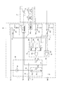
- FIG. 1 is a block diagram showing an overall schematic configuration of a power converter to which the present invention is applied.
- a power converter 1 includes an inverter 2 that converts DC power into AC power, and the inverter 2.
- the inverter 2 includes IGBTs (Insulated Gate Bipolar Transistors) 11 to 16 as six semiconductor elements.
- the IGBTs 11 to 16 are connected to a DC power source and supplied with DC power.
- a series circuit of the IGBTs 11 and 12 a series circuit of the IGBTs 13 and 14, and a series circuit of the IGBTs 15 and 16. are connected in parallel.
- free wheel diodes 21 to 26 are connected to the IGBTs 11 to 16 in antiparallel.
- the upper arms UA are configured by making the IGBTs 11, 13 and 15 into the U phase, the V phase and the W phase, respectively.
- the lower arms LA are configured by making the IGBTs 12, 14, and 16 into the X phase, the Y phase, and the Z phase, respectively.
- three-phase AC power is output from the connection point of the IGBTs 11 and 12, the connection point of the IGBTs 13 and 14, and the connection point of the IGBTs 15 and 16. This three-phase AC power is supplied to an AC load 4 such as an electric motor.
- the IGBTs 11 to 16 are arranged in the chip 17 as shown in FIG.
- a temperature sensor 19 composed of a detection diode is provided.
- the control voltage detection circuit 32, the overcurrent detection circuit 33, and the chip temperature detection circuit 34 detect a low voltage state, an overcurrent state, and an overheat state, which are information necessary for the protection operation of the IGBT 1i.
- Each of the phase driver circuits 3U to 3Z includes a protection signal generation unit 35, a protection state monitoring unit 36, and a signal output unit 40.
- the gate control circuit 31 receives a pulse width modulation (PWM) signal as an operation signal DSG from the outside of the driver circuits 3U to 3Z, and a protection state signal Sp output from the protection state monitoring unit 36. .
- the gate control circuit 31 outputs the operation signal DSG to the gate of the IGBT 1i when the protection state signal Sp is at the low level, and to the gate of the IGBT 1i of the operation signal DSG when the protection state signal Sp is at the high level. Stop the output of.
- the control voltage detection circuit 32 includes a comparator CP1 to which a control voltage Vcc (for example, 15 [V]) is input from the outside of the driver circuits 3U to 3Z and a low voltage threshold Vth1 is input.
- the comparator CP1 When the control voltage Vcc falls below the low voltage threshold Vth1, the comparator CP1 outputs a high-level low voltage detection signal Suv indicating insufficient control voltage to the protection signal generation unit 35 and the protection state monitoring unit 36. Thereby, a shortage of control voltage, that is, a voltage drop of the IC power supply is detected.
- the overcurrent detection circuit 33 includes a comparator CP2 to which the current detection value (voltage signal) detected by the current sensor 18 is input and the overcurrent threshold Vth2 is input.
- the comparator CP2 outputs a high level overcurrent detection signal Soc representing an overcurrent state to the protection signal generation unit 35 and the protection state monitoring unit 36 when the current detection value exceeds the overcurrent threshold Vth2. Thereby, the overcurrent of IGBT1i is detected.
- the chip temperature detection circuit 34 includes a comparator CP3 to which the temperature detection value (voltage signal) detected by the temperature sensor 19 is input and the overheat threshold Vht3 is input.
- the comparator CP3 When the temperature detection value falls below the overheat threshold Vht3, the comparator CP3 outputs a high level overheat detection signal Soh representing an overheat state to the protection signal generation unit 35 and the protection state monitoring unit 36. Thereby, the overheating state of IGBT1i is detected.
- the power source 34a in the chip temperature detection circuit 34 shown in FIG. 2 is for supplying a constant current to the diode when the temperature sensor 19 is constituted by a temperature detection diode.
- the protection signal generator 35 includes a first one-shot circuit 35a, a second one-shot circuit 35b, and a third one-shot circuit 35c configured by a one-shot one-shot circuit, and an OR gate 35d to which these output pulses are input. I have.
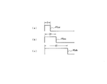
- the first one-shot circuit 35a receives from the control voltage detection circuit 32 a high level low voltage detection signal Suv that detects that the control voltage is insufficient, that is, the IC power supply voltage has become low, FIG.
- a high level pulse signal PSuv having a pulse width of, for example, the basic pulse width T is output to the OR gate 35d.
- the basic pulse width T for example, 2 [ms] can be adopted.
- the second one-shot circuit 35b has a high level as shown in FIG.
- a pulse signal PSoc having a pulse width of 2T, for example, is output to the OR gate 35d.
- the third one-shot circuit 35c has a high level pulse width as shown in FIG. 3C when the overheat detection signal Soh that detects the overheat state of the IGBT 1i is input from the chip temperature detection circuit 34. For example, a 4T pulse signal PSoh is output to the OR gate 35d.
- the OR gate 35d has a high level when one of the pulse signals PSuv, PSoc, and PSoh output from the first one-shot circuit 35a, the second one-shot circuit 35b, and the third one-shot circuit 35c is at a high level.
- the protection signal is output to the signal output unit 40.
- the pulse width of the pulse signal PSj is sufficiently short as 2 to 8 [ms], for example, after an overcurrent state occurs, an overheat state occurs, and two or more pulse signals PSj are generated. However, two or more pulse signals PSj are hardly input simultaneously.
- the protection signal generation unit 35 detects the detection circuits 32 to 34 that detect the control voltage shortage, the overcurrent, or the overheat state among the control voltage detection circuit 32, the overcurrent detection circuit 33, and the chip temperature detection circuit 34.
- the pulse signal PSj corresponding to the detection circuits 32 to 34 that have detected that the operation is necessary is output to the signal output unit 40 as a protection signal.
- the protection state monitoring unit 36 includes a low voltage detection signal Suv output from the control voltage detection circuit 32, an overcurrent detection signal Soc output from the overcurrent detection circuit 33, and an overheat detection signal Soh output from the chip temperature detection circuit 34.
- OR gate 36a The OR gate 36a outputs a high level protection state signal Sp to the gate control circuit 31 and the signal output unit 40 when any one of the low voltage detection signal Suv, the overcurrent detection signal Soc, and the overheat detection signal Soh is at a high level.
- the signal output unit 40 includes a series circuit of a resistor 41 (limit resistor) as a third resistor and an n-channel MOSFET 42 as a first switch element connected in series between the alarm signal output terminal ta and the ground.
- the drain of the MOSFET 42 is connected to the alarm signal output terminal ta via the resistor 41, the source is connected to the ground, and the gate (control terminal) is connected to the output terminal of the OR gate 35 d of the protection signal generator 35. Yes.
- the other end of the constant current source 44 having one end connected to the control power input terminal tvi is connected to a connection point 43 between the resistor 41 and the MOSFET 42.
- the constant current source 44 supplies, for example, a constant current of 200 [ ⁇ A] to the connection point 43.
- the signal output unit 40 is connected to an intermediate voltage generation circuit (constant voltage circuit) 45 in parallel with the MOSFET 42.
- the intermediate voltage generation circuit 45 is configured by a series circuit of a Zener diode 45a and an n-channel MOSFET 45b as a second switch element.
- the breakdown voltage Vmd of the Zener diode 45a is set to an intermediate voltage (for example, 7 [V]) between the control voltage Vcc and the ground potential GND.
- the cathode of the Zener diode 45a is connected to the connection point 43 of the resistor 41 and the MOSFET 42, and the anode is connected to the drain of the MOSFET 45b.
- the source of the MOSFET 45b is connected to the ground, and the gate (control terminal) is connected to the output terminal of the OR gate 36a of the protection state monitoring unit 36 described above.
- the connection point 43 becomes the control voltage Vcc, and the alarm signal output terminal ta becomes the control voltage Vcc at the first level.
- the connection point 43 becomes the ground potential at the second level, and the alarm signal is output.
- the terminal ta is also at the ground potential.
- the anode of the Zener diode 45a is grounded through the MOSFET 45b.
- the alarm signal output terminal ta is also at an intermediate level. Therefore, an alarm signal ALM having three levels of the first level, the second level, and the intermediate level is output from the alarm signal output terminal ta.
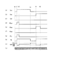
- the overcurrent detection signal Soc output from the chip temperature detection circuit 34 and the overheat detection signal Soh output from the chip temperature detection circuit 34 are both low. Therefore, as shown in FIGS. 4D to 4F, the outputs of the first one-shot circuit 35a, the second one-shot circuit 35b, and the third one-shot circuit 35c of the protection signal generator 35 are maintained at a low level. . Therefore, the protection signal PSj output from the OR gate 35d maintains the low level as shown in FIG. 4G, and the protection state signal Sp also maintains the low level as shown in FIG. 4H. .
- the protection signal PSj output from the protection signal generation unit 35 is maintained at the low level, the MOSFET 42 of the signal output unit 40 is maintained in the off state. Further, since the protection state signal Sp output from the protection state monitoring unit 36 is also maintained at the low level, the MOSFET 45b is also maintained in the off state. Therefore, the potential of the connection point 43 becomes the first level which is the potential of the control voltage Vcc, and the alarm signal ALM output from the alarm signal output terminal ta is the control voltage Vcc representing the normal state as shown in FIG. Potential.
- the gate control circuit 31 since the protection state signal Sp is at a low level, the gate control circuit 31 generates a gate signal corresponding to the operation signal DSG input from an external control device (not shown). Supplyed to the gates of the IGBTs 11 to 16, the inverter 2 converts DC power into AC power, and AC power is output to the AC load 4.
- a high level pulse signal PSuv having a pulse width T is output from the first one-shot circuit 35a of the protection signal generator 35 as shown in FIG. 4 (d).
- the protection state signal Sp output from the protection state monitoring unit 36 is inverted from the low level to the high level as shown in FIG.
- the high-level protection state signal Sp is supplied to the gate control circuit 31, output of the gate drive signal from the gate control circuit 31 is stopped, and the IGBT 11 is turned off to enter the protection state.
- the protection signal PSj output from the protection signal generation unit 35 is at a high level
- the MOSFET 42 of the signal output unit 40 is turned on. Therefore, the connection point 43 is connected to the ground through the MOSFET 42, and the potential at the connection point becomes the second level which is the ground potential GND. Therefore, the potential of the alarm signal ALM changes from the first level to the second level (ground potential GND) indicating that the abnormality has occurred and the protection state has been reached, as shown in FIG.
- the protection state signal Sp output from the protection state monitoring unit 36 is also at a high level
- the MOSFET 45b of the signal output unit 40 is also turned on.
- the anode of the Zener diode 45a is connected to the ground via the MOSFET 45b, but the potential at the connection point 43 is at the second level (ground potential GND). Therefore, the Zener diode 45a stops functioning as an intermediate voltage generation circuit.
- the protection signal PSuv output from the first one-shot circuit 35a of the protection signal generator 35 is changed from the high level as shown in FIG. Return to low level.
- the MOSFET 42 of the signal output unit 40 is turned off. For this reason, the potential of the connection point 43 tends to rise to the control voltage Vcc, but at this time t2, the low voltage state of the control voltage Vcc continues, and the low voltage detection signal Suv output from the control voltage detection circuit 32.
- the high level is maintained as shown in FIG. Therefore, the protection state signal Sp output from the protection state monitoring unit 36 maintains the high level as shown in FIG. 4H, and the MOSFET 45b maintains the on state.
- the Zener diode 45a becomes conductive, and the potential at the connection point 43 becomes an intermediate level that becomes the breakdown voltage Vmd. Therefore, the alarm signal ALM output from the alarm signal output terminal ta becomes an intermediate level that is the breakdown voltage Vmd of the Zener diode 45a, as shown in FIG. It means that it is continuing.
- the low voltage detection signal Suv output from the control voltage detection circuit 32 is shown in FIG.
- the protection state signal Sp output from the protection state monitoring unit 36 also returns from the high level to the low level as shown in FIG. Therefore, a gate drive signal corresponding to the operation signal DSG is output from the gate control circuit 31 to the gate of the IGBT 1i, and the IGBT 1i returns to a normal operation state.
- the protection state signal Sp output from the protection state monitoring unit 36 also returns to the low level, so that the MOSFET 45b of the signal output unit 40 is also turned off. Therefore, the potential at the connection point 43 returns to the control voltage Vcc. Therefore, the alarm signal ALM output from the alarm signal output terminal ta returns to the first level that becomes the control voltage Vcc representing the normal state as shown in FIG.
- the type of abnormality detection circuit may be determined based on the number of counts of the clock signal CP during a period in which the alarm signal ALM maintains the second level that is the ground potential GND.
- the alarm signal ALM when the alarm signal ALM is at the second level by detecting the voltage of the alarm signal ALM, an overcurrent abnormality or an overheating abnormality has occurred in the IGBT 1i, or the control voltage Vcc is a low voltage. It can be recognized that a low voltage state lower than the threshold value Vth1 has occurred. Further, when the alarm signal ALM is at an intermediate level, it can be recognized that an overcurrent abnormality or overheating abnormality of the IGBT 1i has occurred or that the control voltage Vcc is in a low voltage state.
- the overcurrent detection circuit 33 of the driver circuit 3k at the time t4 detects that the detection value of the collector current of the IGBT 1i constituting the inverter 2 is equal to or higher than the overcurrent threshold Vth2
- the overcurrent detection circuit 33 As shown in FIG. 4B, a high level overcurrent detection signal Soc is output.
- the overcurrent detection signal Soc is supplied to the protection signal generator 35. Therefore, the high-level pulse signal PSoc having a pulse width of 2T shown in FIG. 4E is output from the second one-shot circuit 35b of the protection signal generation unit 35. Therefore, the protection signal PSj shown in FIG.
- the external control device can recognize that an overcurrent abnormality has occurred because the second-level pulse width of the ground potential GND of the alarm signal ALM is 2T. Further, the alarm signal ALM is maintained at an intermediate level that is the breakdown voltage Vmd until the protection state due to the overcurrent abnormality is eliminated after the time corresponding to the pulse width 2T has elapsed. For this reason, it can be recognized by the external control device that the protection operation due to the overcurrent abnormality continues even after the protection signal PSoc returns from the high level to the low level.
- the chip temperature detection circuit 34 of a certain driver circuit 3k detects that the temperature detection value in the chip 17 including the IGBT 1i constituting the inverter 2 is less than the overheat threshold Vht3, the chip temperature detection circuit 34 outputs a high-level overheat detection signal Soh.
- the overheat detection signal Soh is supplied to the protection signal generator 35. Therefore, the protection signal PSoh is output from the third one-shot circuit 35 c of the protection signal generation unit 35. Therefore, the MOSFET 42 of the signal output unit 40 is turned on, and the second level alarm signal ALM corresponding to the pulse width 4T of the pulse signal PSoh is output to the external control device.
- the external control device can recognize that an overheat abnormality has occurred because the second-level pulse width of the alarm signal ALM is 4T. Since the voltage of the alarm signal ALM is maintained at an intermediate level that becomes the breakdown voltage Vmd after the time corresponding to the pulse width 4T elapses until the protection operation due to the overheat abnormality is canceled, the protection signal PSoh is It can be recognized that the overheating abnormality continues even after returning from the high level to the low level.
- the power semiconductor element is the IGBT has been described.
- the present invention is not limited to this, and the power semiconductor element may be composed of other power semiconductor elements such as SiC-IGBT, MOSFET, SiC-MOS. it can.
- the case where an n-channel MOSFET is applied as the MOSFET of the signal output unit 40 has been described.
- a p-channel MOSFET can also be applied.
- the first level of the alarm signal ALM is used. Is the ground potential GND, the second level is the control voltage Vcc, and the intermediate level remains the breakdown voltage Vmd.
- the output signals of the protection signal generation unit 35 and the protection state monitoring unit 36 may be supplied to the p-channel MOSFETs 42 and 45b via the logic inversion circuits, respectively.
- the Zener diode 45a constituting the intermediate voltage generating circuit 45 is connected to the connection point 43 side is described.
- the Zener diode 45a may be connected to the ground side of the MOSFET 45b.
- a resistor (second resistor) can be applied instead of the Zener diode 45a.
- the pulse widths of the first one-shot circuit 35a, the second one-shot circuit 35b, and the third one-shot circuit 35c of the protection signal generation unit 35 are not limited to T, 2T, and 4T. Any different pulse width can be set as long as it can be identified.
- the protection signal generation unit 35 may be provided with an input selection circuit that blocks the input of other abnormality detection signals for a predetermined period when one abnormality detection signal is input.
- the signals to the gates of the MOSFETs 42 and 45b may be interchanged. In this case, information about the state represented by the intermediate level and the second level is also switched.
- SYMBOLS 1 Power converter device, 2 ... Inverter, 3U-3Z ... Driver circuit, 4 ... AC load, 11-16 ... IGBT, 17 ... Chip, 18 ... Current sensor, 19 ... Temperature sensor, 21-26 ... Freewheel diode, UA ... Upper arm, LA ... Lower arm, 31 ... Gate control circuit, 32 ... Control voltage detection circuit, 33 ... Overcurrent detection circuit, 34 ... Chip temperature detection circuit, 35 ... Protection signal generator, 35a ... First one-shot Circuit, 35b ... second one-shot circuit, 35c ... third one-shot circuit, 35d ... OR gate, 36 ... protection state monitoring unit, 36a ... OR gate, 40 ... signal output unit, 41 ... resistor, 42 ... MOSFET, 43 ... connection Point, 44: constant current source, 45: intermediate voltage generation circuit, 45a: Zener diode, 45b: MOSFET, PSj: protection signal, Sp: protection State signal
Landscapes
- Engineering & Computer Science (AREA)
- Power Engineering (AREA)
- Physics & Mathematics (AREA)
- General Physics & Mathematics (AREA)
- Electromagnetism (AREA)
- Microelectronics & Electronic Packaging (AREA)
- Inverter Devices (AREA)
- Power Conversion In General (AREA)
- Electronic Switches (AREA)
Abstract
電力変換装置を構成する半導体素子の保護動作に必要な情報を検出する複数の検出回路(32,33,34)と、複数の検出回路が保護動作に必要な情報を検出したときに、これら複数の検出回路毎に異なるパルス幅の保護信号を生成する保護信号生成部(35)と、複数の検出回路の何れかで保護動作に必要な情報を検出している間保護状態信号を生成する保護状態監視部(36)と、保護信号が入力されたときに第1レベルから第2レベルに状態変化し、保護信号の入力が停止されかつ保護状態信号が入力されているときに、第1レベル及び第2レベル間の中間レベルとなるアラーム信号を出力する信号出力部(40)とを備えている。
Description
本発明は、例えば、電力変換装置を構成する半導体素子を駆動するとともに、保護動作識別機能を有する半導体素子の駆動装置に関する。
近時、インテリジェント・パワーモジュール(IPM)が注目されている。このインテリジェント・パワーモジュールは、半導体素子(IGBT等のパワートランジスタ)とその駆動回路とともに、半導体素子の過電流、制御電源の電圧低下、過熱等の異常に対する保護回路を1つの電子部品としてモジュール化したものである。
また、このような異常をそれぞれ検出する複数の保護回路に加えて、各保護回路にて検出した異常の種別に応じて予め定めたパルス幅のアラーム信号を外部出力する判別回路(出力回路)をインテリジェント・パワーモジュールに組み込むことも提唱されている(例えば、特許文献1の図3参照)。
また、このような異常をそれぞれ検出する複数の保護回路に加えて、各保護回路にて検出した異常の種別に応じて予め定めたパルス幅のアラーム信号を外部出力する判別回路(出力回路)をインテリジェント・パワーモジュールに組み込むことも提唱されている(例えば、特許文献1の図3参照)。
このようなアラーム信号を出力する判別回路を備えることで、駆動装置を制御する制御装置側、例えば、インバータ制御装置ではアラーム信号のパルス幅を検出することで半導体素子に生じた異常の種別を判別することができる(例えば、特許文献2参照)。
しかしながら、上記のようにアラーム信号を出力するだけでは、半導体素子の異常が解消されても、これを検出することができないという問題を含んでいる。そこで、本出願人は、先に上記不具合を回避し、また一般的にはパルス信号列として出力されるアラーム信号の判別および異常解消の検出を容易化する半導体素子の駆動装置を提唱した(特許文献3を参照)。
しかしながら、上記のようにアラーム信号を出力するだけでは、半導体素子の異常が解消されても、これを検出することができないという問題を含んでいる。そこで、本出願人は、先に上記不具合を回避し、また一般的にはパルス信号列として出力されるアラーム信号の判別および異常解消の検出を容易化する半導体素子の駆動装置を提唱した(特許文献3を参照)。
この半導体素子の駆動装置は、最初に異常を検出した検出回路の出力に応じて、異常検出開始時にアラーム信号の1パルス分だけローレベルとなる電圧を出力してから高レベルに復帰するとともに、異常検出信号の出力が停止したときに一定期間に亘って出力回路の信号出力レベルを保護解除を表す中レベルに変更するものである。
このような出力回路の信号出力レベルを変更することで、複数のアラーム信号の判別の容易化に加え、半導体素子の異常が解消されたときすなわち保護動作の終了時を検出することができる。
このような出力回路の信号出力レベルを変更することで、複数のアラーム信号の判別の容易化に加え、半導体素子の異常が解消されたときすなわち保護動作の終了時を検出することができる。
特許文献3で提唱した半導体素子の駆動装置によれば、出力信号を監視することにより、保護動作開始時の保護動作種別と保護動作解除とを検出することができる。しかしながら、出力信号が保護動作種別を表す低レベルから高レベルに復帰してから中レベルとなる保護動作解除信号が出力されるまでの間は、出力信号が高レベルを維持する。したがって、この期間では、出力信号を検出するだけでは、保護動作状態であるか否かを判断できない。
本発明は、上記従来例の未解決の課題に着目してなされたものであり、駆動装置から出力されるアラーム信号を監視することにより、保護動作状態であるか否かを容易に判別できる半導体素子の駆動装置を提供することを目的としている。
本発明は、上記従来例の未解決の課題に着目してなされたものであり、駆動装置から出力されるアラーム信号を監視することにより、保護動作状態であるか否かを容易に判別できる半導体素子の駆動装置を提供することを目的としている。
上記目的を達成するために、本発明の半導体素子の駆動装置の一態様は、電力変換装置を構成する半導体素子の保護動作に必要な情報を検出する複数の検出部と、複数の検出部で保護動作に必要な情報を検出したときに、これら複数の検出部毎に異なるパルス幅の保護信号を生成する保護信号生成部と、複数の検出部の何れかで保護動作に必要な情報を検出している間保護状態信号を生成する保護状態監視部と、保護信号及び保護状態信号が入力されたときに第1レベルから第2レベルに状態変化し、前記保護信号の入力が停止されたときに、第1レベル及び第2レベル間の中間レベルとなるアラーム信号を出力する信号出力部とを備えている。
本発明の一態様によれば、アラーム信号の第1レベルのパルス幅を検出することで半導体素子に生じた保護動作の種別を容易に判別できる。また、アラーム信号の第2レベルを検出することで、保護動作状態を継続していることを判別することができる。
次に、図面を参照して、本発明の一実施の形態を説明する。以下の図面の記載において、同一又は類似の部分には同一又は類似の符号を付している。
また、以下に示す実施の形態は、本発明の技術的思想を具体化するための装置や方法を例示するものであって、本発明の技術的思想は、構成部品の材質、形状、構造、配置等を下記のものに特定するものでない。本発明の技術的思想は、特許請求の範囲に記載された請求項が規定する技術的範囲内において、種々の変更を加えることができる。
以下、本発明の実施の形態について、図面を参照して説明する。
また、以下に示す実施の形態は、本発明の技術的思想を具体化するための装置や方法を例示するものであって、本発明の技術的思想は、構成部品の材質、形状、構造、配置等を下記のものに特定するものでない。本発明の技術的思想は、特許請求の範囲に記載された請求項が規定する技術的範囲内において、種々の変更を加えることができる。
以下、本発明の実施の形態について、図面を参照して説明する。
図1は、本発明が適用される電力変換装置の全体的な概略構成を示すブロック図であるこの図1において、電力変換装置1は、直流電力を交流電力に変換するインバータ2とこのインバータ2を構成する各相(U相~Z相)の半導体素子を個別に駆動する半導体素子の駆動装置としての各相ドライバ回路3U~3Zとを備えている。
インバータ2は、6個の半導体素子としてのIGBT(Insulated Gate Bipolar Transistor)11~16を有する。
これらIGBT11~16は、直流電源に接続されて直流電力が供給される正極側ラインLp及び負極側ラインLn間に、IGBT11及び12の直列回路、IGBT13及び14の直列回路並びにIGBT15及び16の直列回路がそれぞれ並列に接続されている。ここで、各IGBT11~16には、フリーホイールダイオード21~26が逆並列に接続されている。
インバータ2は、6個の半導体素子としてのIGBT(Insulated Gate Bipolar Transistor)11~16を有する。
これらIGBT11~16は、直流電源に接続されて直流電力が供給される正極側ラインLp及び負極側ラインLn間に、IGBT11及び12の直列回路、IGBT13及び14の直列回路並びにIGBT15及び16の直列回路がそれぞれ並列に接続されている。ここで、各IGBT11~16には、フリーホイールダイオード21~26が逆並列に接続されている。
また、IGBT11、13及び15がそれぞれU相、V相及びW相とされて上アームUAが構成されている。また、IGBT12、14及び16がそれぞれX相、Y相及びZ相とされて下アームLAが構成されている。さらに、IGBT11及び12の接続点、IGBT13及び14の接続点並びにIGBT15及び16の接続点から三相交流電力が出力されている。この三相交流電力が、電動モータ等の交流負荷4に供給されている。
IGBT11~16は、図2に示すように、チップ17内に配設されている。このチップ17内には、IGBT1i(i=1~6)のコレクタ及びエミッタ間を流れる電流を検出する電流センス用IBGTや電流センス抵抗で構成される電流センサ18と、チップ内温度を検出する温度検出用ダイオードで構成される温度センサ19とが設けられている。
IGBT11~16は、図2に示すように、チップ17内に配設されている。このチップ17内には、IGBT1i(i=1~6)のコレクタ及びエミッタ間を流れる電流を検出する電流センス用IBGTや電流センス抵抗で構成される電流センサ18と、チップ内温度を検出する温度検出用ダイオードで構成される温度センサ19とが設けられている。
各相ドライバ回路3k(k=U~Z)は、図2に示すように、インバータ2を構成する各IGBT1iのゲートをオン/オフ制御するゲート制御回路31と、検出部としての制御電圧検出回路32、過電流検出回路33及びチップ温度検出回路34とを備えている。これら制御電圧検出回路32、過電流検出回路33及びチップ温度検出回路34は、IGBT1iの保護動作に必要な情報である低電圧状態、過電流状態及び過熱状態を検出するものである。
また、各相ドライバ回路3U~3Zは、保護信号生成部35と、保護状態監視部36と、信号出力部40を備えている。
また、各相ドライバ回路3U~3Zは、保護信号生成部35と、保護状態監視部36と、信号出力部40を備えている。
ゲート制御回路31には、ドライバ回路3U~3Zの外部からパルス幅変調(PWM)信号が動作信号DSGとして入力されるとともに、保護状態監視部36から出力される保護状態信号Spが入力されている。このゲート制御回路31は、保護状態信号Spがローレベルであるときに、動作信号DSGをIGBT1iのゲートに出力し、保護状態信号Spがハイレベルであるときに、動作信号DSGのIGBT1iのゲートへの出力を停止する。
制御電圧検出回路32は、ドライバ回路3U~3Zの外部から制御電圧Vcc(例えば15[V])が入力されるとともに、低電圧閾値Vth1が入力された比較器CP1を有する。この比較器CP1は、制御電圧Vccが低電圧閾値Vth1を下回ると、制御電圧不足を表すハイレベルの低電圧検出信号Suvを保護信号生成部35と保護状態監視部36とに出力する。これにより、制御電圧不足、つまり、IC電源の電圧低下を検出する。
制御電圧検出回路32は、ドライバ回路3U~3Zの外部から制御電圧Vcc(例えば15[V])が入力されるとともに、低電圧閾値Vth1が入力された比較器CP1を有する。この比較器CP1は、制御電圧Vccが低電圧閾値Vth1を下回ると、制御電圧不足を表すハイレベルの低電圧検出信号Suvを保護信号生成部35と保護状態監視部36とに出力する。これにより、制御電圧不足、つまり、IC電源の電圧低下を検出する。
過電流検出回路33は、電流センサ18で検出した電流検出値(電圧信号)が入力されるとともに、過電流閾値Vth2が入力された比較器CP2を有する。この比較器CP2は、電流検出値が過電流閾値Vth2を上回ると過電流状態を表すハイレベルの過電流検出信号Socを保護信号生成部35と保護状態監視部36とに出力する。これにより、IGBT1iの過電流を検出する。
チップ温度検出回路34は、温度センサ19で検出した温度検出値(電圧信号)が入力されるとともに過熱閾値Vht3が入力された比較器CP3を有する。この比較器CP3は、温度検出値が過熱閾値Vht3を下回ると過熱状態を表すハイレベルの過熱検出信号Sohを保護信号生成部35と保護状態監視部36とに出力する。これにより、IGBT1iの過熱状態を検出する。
チップ温度検出回路34は、温度センサ19で検出した温度検出値(電圧信号)が入力されるとともに過熱閾値Vht3が入力された比較器CP3を有する。この比較器CP3は、温度検出値が過熱閾値Vht3を下回ると過熱状態を表すハイレベルの過熱検出信号Sohを保護信号生成部35と保護状態監視部36とに出力する。これにより、IGBT1iの過熱状態を検出する。
なお、図2に示した、チップ温度検出回路34内の電源34aは、温度センサ19を温度検出用ダイオードで構成した場合に、このダイオードに定電流を供給するためのものである。
保護信号生成部35は、1ショットワンショット回路で構成される第1ワンショット回路35a、第2ワンショット回路35b、第3ワンショット回路35cと、これらの出力パルスが入力されるオアゲート35dとを備えている。
第1ワンショット回路35aは、制御電圧検出回路32から制御電圧不足、つまり、IC電源の低電圧となったことを検出したハイレベルの低電圧検出信号Suvが入力されたときに、図3(a)に示すように、ハイレベルの、パルス幅が例えば基本パルス幅Tとなるパルス信号PSuvをオアゲート35dに出力する。基本パルス幅Tとしては、例えば、2[ms]を採用できる。
保護信号生成部35は、1ショットワンショット回路で構成される第1ワンショット回路35a、第2ワンショット回路35b、第3ワンショット回路35cと、これらの出力パルスが入力されるオアゲート35dとを備えている。
第1ワンショット回路35aは、制御電圧検出回路32から制御電圧不足、つまり、IC電源の低電圧となったことを検出したハイレベルの低電圧検出信号Suvが入力されたときに、図3(a)に示すように、ハイレベルの、パルス幅が例えば基本パルス幅Tとなるパルス信号PSuvをオアゲート35dに出力する。基本パルス幅Tとしては、例えば、2[ms]を採用できる。
また、第2ワンショット回路35bは、過電流検出回路33からIGBT1iの過電流状態を検出した過電流検出信号Socが入力されたときに、図3(b)に示すように、ハイレベルの、パルス幅が例えば2Tとなるパルス信号PSocをオアゲート35dに出力する。
さらに、第3ワンショット回路35cは、チップ温度検出回路34からIGBT1iの過熱状態を検出した過熱検出信号Sohが入力されたときに、図3(c)に示すようにハイレベルの、パルス幅が例えば4Tとなるパルス信号PSohをオアゲート35dに出力する。
さらに、第3ワンショット回路35cは、チップ温度検出回路34からIGBT1iの過熱状態を検出した過熱検出信号Sohが入力されたときに、図3(c)に示すようにハイレベルの、パルス幅が例えば4Tとなるパルス信号PSohをオアゲート35dに出力する。
オアゲート35dは、第1ワンショット回路35a、第2ワンショット回路35b及び第3ワンショット回路35cから出力されるパルス信号PSuv、PSoc及びPSohのうち何れかがハイレベルであるときに、ハイレベルの保護信号を信号出力部40に出力する。
ここで、パルス信号PSjのパルス幅は2~8[ms]と十分に短いため、例えば、過電流状態が生じた後それを原因として過熱状態が発生し、2以上のパルス信号PSjが発生しても、2以上のパルス信号PSjが同時に入力されることは殆どない。これにより、保護信号生成部35は、制御電圧検出回路32、過電流検出回路33及びチップ温度検出回路34のうち制御電圧不足、過電流または過熱状態を検出した検出回路32~34、つまり、保護動作が必要であることを検出した検出回路32~34に対応するパルス信号PSjを保護信号として信号出力部40に出力する。
ここで、パルス信号PSjのパルス幅は2~8[ms]と十分に短いため、例えば、過電流状態が生じた後それを原因として過熱状態が発生し、2以上のパルス信号PSjが発生しても、2以上のパルス信号PSjが同時に入力されることは殆どない。これにより、保護信号生成部35は、制御電圧検出回路32、過電流検出回路33及びチップ温度検出回路34のうち制御電圧不足、過電流または過熱状態を検出した検出回路32~34、つまり、保護動作が必要であることを検出した検出回路32~34に対応するパルス信号PSjを保護信号として信号出力部40に出力する。
保護状態監視部36は、制御電圧検出回路32から出力される低電圧検出信号Suv、過電流検出回路33から出力される過電流検出信号Soc及びチップ温度検出回路34から出力される過熱検出信号Sohが入力されたオアゲート36aを有する。このオアゲート36aは、低電圧検出信号Suv、過電流検出信号Soc及び過熱検出信号Sohのうち何れかがハイレベルであるときに、ハイレベルの保護状態信号Spをゲート制御回路31と信号出力部40とに出力する。
信号出力部40は、アラーム信号出力端子ta及び接地間に直列に接続された第3の抵抗としての抵抗41(制限抵抗)及び第1スイッチ素子としてのnチャネルのMOSFET42の直列回路を有する。ここで、MOSFET42のドレインは、抵抗41を介してアラーム信号出力端子taに接続され、ソースは接地に接続され、ゲート(制御端子)は保護信号生成部35のオアゲート35dの出力端子に接続されている。
信号出力部40は、アラーム信号出力端子ta及び接地間に直列に接続された第3の抵抗としての抵抗41(制限抵抗)及び第1スイッチ素子としてのnチャネルのMOSFET42の直列回路を有する。ここで、MOSFET42のドレインは、抵抗41を介してアラーム信号出力端子taに接続され、ソースは接地に接続され、ゲート(制御端子)は保護信号生成部35のオアゲート35dの出力端子に接続されている。
そして、抵抗41及びMOSFET42の接続点43に一端が制御電源入力端子tviに接続された定電流源44の他端が接続されている。この定電流源44は、例えば、200[μA]の定電流を接続点43に供給する。
また、信号出力部40は、MOSFET42と並列に中間電圧生成回路(定電圧回路)45が接続されている。この中間電圧生成回路45は、ツェナーダイオード45aと第2スイッチ素子としてのnチャネルのMOSFET45bとの直列回路で構成されている。
ツェナーダイオード45aの降伏電圧Vmdは、制御電圧Vccとグランド電位GNDとの中間の電圧(例えば、7[V])に設定されている。このツェナーダイオード45aのカソードが、抵抗41及びMOSFET42の接続点43に接続され、アノードが、MOSFET45bのドレインに接続されている。MOSFET45bのソースが接地に接続され、ゲート(制御端子)が前述した保護状態監視部36のオアゲート36aの出力端子に接続されている。
また、信号出力部40は、MOSFET42と並列に中間電圧生成回路(定電圧回路)45が接続されている。この中間電圧生成回路45は、ツェナーダイオード45aと第2スイッチ素子としてのnチャネルのMOSFET45bとの直列回路で構成されている。
ツェナーダイオード45aの降伏電圧Vmdは、制御電圧Vccとグランド電位GNDとの中間の電圧(例えば、7[V])に設定されている。このツェナーダイオード45aのカソードが、抵抗41及びMOSFET42の接続点43に接続され、アノードが、MOSFET45bのドレインに接続されている。MOSFET45bのソースが接地に接続され、ゲート(制御端子)が前述した保護状態監視部36のオアゲート36aの出力端子に接続されている。
このため、MOSFET42及び45bがともにオフ状態であるときには、接続点43が制御電圧Vccとなり、アラーム信号出力端子taが第1レベルとなる制御電圧Vccとなる。一方、MOSFET42がオン状態であるときには、定電流源44からの定電流が接地に流れるので、MOSFET45bのオン・オフ状態にかかわらず、接続点43は第2レベルとなるグランド電位となり、アラーム信号出力端子taもグランド電位となる。
また、MOSFET45bがオン状態であり、MOSFET42がオフ状態であるときには、ツェナーダイオード45aのアノードがMOSFET45bを通じて接地されるので、接続点43が降伏電圧Vmdとなる第1レベル及び第2レベルの中間レベルとなり、アラーム信号出力端子taも中間レベルとなる。
したがって、アラーム信号出力端子taから第1レベル、第2レベル及びこれらの中間レベルの3つのレベルをとるアラーム信号ALMが出力される。
また、MOSFET45bがオン状態であり、MOSFET42がオフ状態であるときには、ツェナーダイオード45aのアノードがMOSFET45bを通じて接地されるので、接続点43が降伏電圧Vmdとなる第1レベル及び第2レベルの中間レベルとなり、アラーム信号出力端子taも中間レベルとなる。
したがって、アラーム信号出力端子taから第1レベル、第2レベル及びこれらの中間レベルの3つのレベルをとるアラーム信号ALMが出力される。
次に、本実施形態の電力変換装置1の動作について説明する。
今、インバータ2を構成するIGBT11~16に流れる電流の検出値が過電流閾値Vth2未満で正常であり、且つ、IGBT11~16を形成したチップ17内の温度の検出値が過熱閾値Vht3以上で正常であり、さらに各ドライバ回路3U~3Zに供給する制御電圧Vcc(IC電源電圧)が低電圧閾値Vth1を超えていて正常であるものとする。
この正常状態では、図4(a)~(c)に示すように、時点t0で、各ドライバ回路3U~3Zの制御電圧検出回路32から出力される低電圧検出信号Suv、過電流検出回路33から出力される過電流検出信号Soc及びチップ温度検出回路34から出力される過熱検出信号Sohがともにローレベルとなっている。
そのため、図4(d)~(f)に示すように、保護信号生成部35の第1ワンショット回路35a、第2ワンショット回路35b及び第3ワンショット回路35cの出力はローレベルを維持する。したがって、オアゲート35dから出力される保護信号PSjは図4(g)に示すようにローレベルを維持しているとともに保護状態信号Spも図4(h)に示すようにローレベルを維持している。
今、インバータ2を構成するIGBT11~16に流れる電流の検出値が過電流閾値Vth2未満で正常であり、且つ、IGBT11~16を形成したチップ17内の温度の検出値が過熱閾値Vht3以上で正常であり、さらに各ドライバ回路3U~3Zに供給する制御電圧Vcc(IC電源電圧)が低電圧閾値Vth1を超えていて正常であるものとする。
この正常状態では、図4(a)~(c)に示すように、時点t0で、各ドライバ回路3U~3Zの制御電圧検出回路32から出力される低電圧検出信号Suv、過電流検出回路33から出力される過電流検出信号Soc及びチップ温度検出回路34から出力される過熱検出信号Sohがともにローレベルとなっている。
そのため、図4(d)~(f)に示すように、保護信号生成部35の第1ワンショット回路35a、第2ワンショット回路35b及び第3ワンショット回路35cの出力はローレベルを維持する。したがって、オアゲート35dから出力される保護信号PSjは図4(g)に示すようにローレベルを維持しているとともに保護状態信号Spも図4(h)に示すようにローレベルを維持している。
このとき、保護信号生成部35から出力される保護信号PSjがローレベルを維持しているので、信号出力部40のMOSFET42はオフ状態を維持している。また、保護状態監視部36から出力される保護状態信号Spもローレベルを維持しているので、MOSFET45bもオフ状態を維持している。それゆえ、接続点43の電位が制御電圧Vccの電位である第1レベルとなり、アラーム信号出力端子taから出力されるアラーム信号ALMが図4(i)に示すように正常状態を表す制御電圧Vccの電位となる。
このため、各ドライバ回路3X~3Zでは、保護状態信号Spがローレベルであることからゲート制御回路31で、外部の制御装置(図示せず)から入力される動作信号DSGに応じたゲート信号をIGBT11~16のゲートに供給し、インバータ2で直流電力が交流電力に変換されて、交流負荷4に交流電力が出力される。
このため、各ドライバ回路3X~3Zでは、保護状態信号Spがローレベルであることからゲート制御回路31で、外部の制御装置(図示せず)から入力される動作信号DSGに応じたゲート信号をIGBT11~16のゲートに供給し、インバータ2で直流電力が交流電力に変換されて、交流負荷4に交流電力が出力される。
その後、このインバータ2の各相のIGBT11~16が正常状態であり、IC電源電圧が正常である状態から、時点t1で、例えば、X相のIGBT11を駆動するドライバ回路3Uに供給されるIC電源電圧である制御電圧Vccが低電圧閾値Vth1以下に低下する低電圧異常が発生したときには、この低電圧異常が制御電圧検出回路32で検出される。
すると、制御電圧検出回路32からハイレベルの低電圧検出信号Suvが保護信号生成部35と保護状態監視部36とに供給される。このため、保護信号生成部35の第1ワンショット回路35aから第4図(d)に示すようにハイレベルの、パルス幅Tのパルス信号PSuvが出力される。また同時に、保護状態監視部36から出力される保護状態信号Spが、図4(h)に示すようにローレベルからハイレベルに反転される。
すると、制御電圧検出回路32からハイレベルの低電圧検出信号Suvが保護信号生成部35と保護状態監視部36とに供給される。このため、保護信号生成部35の第1ワンショット回路35aから第4図(d)に示すようにハイレベルの、パルス幅Tのパルス信号PSuvが出力される。また同時に、保護状態監視部36から出力される保護状態信号Spが、図4(h)に示すようにローレベルからハイレベルに反転される。
このため、ハイレベルの保護状態信号Spがゲート制御回路31に供給され、ゲート制御回路31からのゲート駆動信号の出力が停止され、IGBT11がターンオフされて保護状態となる。
このとき、保護信号生成部35から出力される保護信号PSjがハイレベルとなるので、信号出力部40のMOSFET42はターンオン状態となる。それゆえ、接続点43がMOSFET42を通じて接地に接続され、接続点の電位がグランド電位GNDである第2レベルとなる。そのため、アラーム信号ALMの電位は図4(i)に示すように第1レベルから異常が発生して保護状態となったことを表す第2レベル(グランド電位GND)に状態変化する。
このとき、保護信号生成部35から出力される保護信号PSjがハイレベルとなるので、信号出力部40のMOSFET42はターンオン状態となる。それゆえ、接続点43がMOSFET42を通じて接地に接続され、接続点の電位がグランド電位GNDである第2レベルとなる。そのため、アラーム信号ALMの電位は図4(i)に示すように第1レベルから異常が発生して保護状態となったことを表す第2レベル(グランド電位GND)に状態変化する。
なお、その際、保護状態監視部36から出力される保護状態信号Spもハイレベルとなるので、信号出力部40のMOSFET45bもターンオン状態となる。これによって、ツェナーダイオード45aのアノードがMOSFET45bを介して接地に接続されることになるが、接続点43の電位が第2レベル(グランド電位GND)となっている。そのため、ツェナーダイオード45aは、中間電圧生成回路として機能を停止している。
その後、時点t1からパルス幅T分の時間が経過した時点t2で、保護信号生成部35の第1ワンショット回路35aから出力される保護信号PSuvが図4(d)に示すようにハイレベルからローレベルに復帰する。これに応じて信号出力部40のMOSFET42はターンオフ状態となる。このため、接続点43の電位が制御電圧Vccまで上昇しようとするが、この時点t2では制御電圧Vccの低電圧状態が継続しており、制御電圧検出回路32から出力される低電圧検出信号Suvが図4(a)に示すようにハイレベルを維持している。それゆえ、保護状態監視部36から出力される保護状態信号Spが図4(h)に示すようにハイレベルを維持し、MOSFET45bはオン状態を維持している。そのため、ツェナーダイオード45aに印加される電圧が降伏電圧Vmd以上となると、ツェナーダイオード45aが導通し、接続点43の電位が降伏電圧Vmdとなる中間レベルとなる。このため、アラーム信号出力端子taから出力されるアラーム信号ALMは、図4(i)に示すように、ツェナーダイオード45aの降伏電圧Vmdである中間レベルとなり、異常状態の発生が継続して保護状態を継続していることを表すことになる。
その後、時点t1からパルス幅T分の時間が経過した時点t2で、保護信号生成部35の第1ワンショット回路35aから出力される保護信号PSuvが図4(d)に示すようにハイレベルからローレベルに復帰する。これに応じて信号出力部40のMOSFET42はターンオフ状態となる。このため、接続点43の電位が制御電圧Vccまで上昇しようとするが、この時点t2では制御電圧Vccの低電圧状態が継続しており、制御電圧検出回路32から出力される低電圧検出信号Suvが図4(a)に示すようにハイレベルを維持している。それゆえ、保護状態監視部36から出力される保護状態信号Spが図4(h)に示すようにハイレベルを維持し、MOSFET45bはオン状態を維持している。そのため、ツェナーダイオード45aに印加される電圧が降伏電圧Vmd以上となると、ツェナーダイオード45aが導通し、接続点43の電位が降伏電圧Vmdとなる中間レベルとなる。このため、アラーム信号出力端子taから出力されるアラーム信号ALMは、図4(i)に示すように、ツェナーダイオード45aの降伏電圧Vmdである中間レベルとなり、異常状態の発生が継続して保護状態を継続していることを表すことになる。
その後、時点t3で、外部から供給される制御電圧Vccが低電圧閾値Vth1より高い正常な電圧に復帰すると、制御電圧検出回路32から出力される低電圧検出信号Suvが図4(a)に示すようにハイレベルからローレベルに復帰する。これに応じて保護状態監視部36から出力される保護状態信号Spも図4(h)に示すようにハイレベルからローレベルに復帰する。このため、ゲート制御回路31から動作信号DSGに応じたゲート駆動信号がIGBT1iのゲート に出力されて、IGBT1iが正常な動作状態に復帰する。
この結果、保護状態監視部36から出力される保護状態信号Spもローレベルに復帰するので、信号出力部40のMOSFET45bもターンオフ状態となる。それゆえ、接続点43の電位が制御電圧Vccに復帰する。そのため、アラーム信号出力端子taからから出力されるアラーム信号ALMが図4(i)に示すように正常状態を表す制御電圧Vccとなる第1レベルに復帰する。
この結果、保護状態監視部36から出力される保護状態信号Spもローレベルに復帰するので、信号出力部40のMOSFET45bもターンオフ状態となる。それゆえ、接続点43の電位が制御電圧Vccに復帰する。そのため、アラーム信号出力端子taからから出力されるアラーム信号ALMが図4(i)に示すように正常状態を表す制御電圧Vccとなる第1レベルに復帰する。
一方、外部の制御装置では、ドライバ回路3kからアラーム信号ALMが入力されると、このアラーム信号ALMがグランド電位GNDである第2レベルを維持している間に、図4(j)に示すクロック信号CPをカウントする。そして、このカウント数とクロック信号CPのパルス間の時間を乗算して積算時間を算出し、この積算時間からアラーム信号ALMが低電圧検出信号Suvによるものであることを検出することができる。これにより、IGBT1iに生じた異常の種別が、低電圧異常であることを容易に判別することができる。なお、アラーム信号ALMがグランド電位GNDである第2レベルを維持している期間のクロック信号CPのカウント数で異常検出回路の種別を判別するようにしてもよい。
また、外部の制御装置では、アラーム信号ALMの電圧を検出することにより、アラーム信号ALMが第2レベルにあるときに、IGBT1iに過電流異常や過熱異常が発生したか又は制御電圧Vccが低電圧閾値Vth1より低下した低電圧状態が発生したことを認識することができる。また、アラーム信号ALMが中間レベルであるときには、IGBT1iの過電流異常や過熱異常が発生した状態又は制御電圧Vccが低電圧状態である状態を継続しているものと認識することができる。
同様に、時点t4であるドライバ回路3kの過電流検出回路33でインバータ2を構成するIGBT1iのコレクタ電流の検出値が過電流閾値Vth2以上となったことを検出した場合は、過電流検出回路33から図4(b)に示すように、ハイレベルの過電流検出信号Socが出力される。この過電流検出信号Socが保護信号生成部35に供給される。このため、保護信号生成部35の第2ワンショット回路35bから図4(e)に示すハイレベルの、パルス幅が2Tとなるパルス信号PSocが出力される。したがって、保護信号生成部35のオアゲート35dから図4(g)に示す保護信号PSjが出力され、これが信号出力部40のMOSFET42のゲートに供給される。このため、MOSFET42がターンオン状態となり、図4(i)に示すように、アラーム信号出力端子taから保護信号PSocのパルス幅2Tに対応する期間第2レベルとなるアラーム信号ALMが外部の制御装置に出力される。
同様に、時点t4であるドライバ回路3kの過電流検出回路33でインバータ2を構成するIGBT1iのコレクタ電流の検出値が過電流閾値Vth2以上となったことを検出した場合は、過電流検出回路33から図4(b)に示すように、ハイレベルの過電流検出信号Socが出力される。この過電流検出信号Socが保護信号生成部35に供給される。このため、保護信号生成部35の第2ワンショット回路35bから図4(e)に示すハイレベルの、パルス幅が2Tとなるパルス信号PSocが出力される。したがって、保護信号生成部35のオアゲート35dから図4(g)に示す保護信号PSjが出力され、これが信号出力部40のMOSFET42のゲートに供給される。このため、MOSFET42がターンオン状態となり、図4(i)に示すように、アラーム信号出力端子taから保護信号PSocのパルス幅2Tに対応する期間第2レベルとなるアラーム信号ALMが外部の制御装置に出力される。
このため、外部の制御装置では、アラーム信号ALMのグランド電位GNDとなる第2レベルのパルス幅が2Tであることから、過電流異常が発生していると認識することができる。また、アラーム信号ALMは、パルス幅2Tに応じた時間が経過した後に、過電流異常による保護状態が解消されるまでは、降伏電圧Vmdとなる中間レベルに維持される。このため、外部の制御装置で、保護信号PSocがハイレベルからローレベルに復帰した後も、過電流異常による保護動作が継続していると認識できる。
同様に、あるドライバ回路3kのチップ温度検出回路34でインバータ2を構成するIGBT1iを内蔵するチップ17内の温度の検出値が過熱閾値Vht3未満となったことを検出した場合は、チップ温度検出回路34からハイレベルの過熱検出信号Sohが出力される。この過熱検出信号Sohが保護信号生成部35に供給される。このため、保護信号生成部35の第3ワンショット回路35cから保護信号PSohが出力される。したがって、信号出力部40のMOSFET42がターンオン状態となり、パルス信号PSohのパルス幅4Tに対応する第2レベルのアラーム信号ALMが外部の制御装置に出力される。
同様に、あるドライバ回路3kのチップ温度検出回路34でインバータ2を構成するIGBT1iを内蔵するチップ17内の温度の検出値が過熱閾値Vht3未満となったことを検出した場合は、チップ温度検出回路34からハイレベルの過熱検出信号Sohが出力される。この過熱検出信号Sohが保護信号生成部35に供給される。このため、保護信号生成部35の第3ワンショット回路35cから保護信号PSohが出力される。したがって、信号出力部40のMOSFET42がターンオン状態となり、パルス信号PSohのパルス幅4Tに対応する第2レベルのアラーム信号ALMが外部の制御装置に出力される。
このため、外部の制御装置では、アラーム信号ALMの第2レベルのパルス幅が4Tであることから、過熱異常が発生していると認識することができる。また、パルス幅4Tに対応する時間が経過した後、過熱異常による保護動作が解消されるまでは、アラーム信号ALMの電圧が降伏電圧Vmdとなる中間レベルに維持されることから、保護信号PSohがハイレベルからローレベルに復帰した後も、過熱異常が継続していると認識できる。
なお、上記実施形態では、パワー半導体素子がIGBTである場合について説明したが、これに限定されるものではなく、SiC-IGBT、MOSFET、SiC-MOS等の他のパワー半導体素子で構成することもできる。
なお、上記実施形態では、パワー半導体素子がIGBTである場合について説明したが、これに限定されるものではなく、SiC-IGBT、MOSFET、SiC-MOS等の他のパワー半導体素子で構成することもできる。
また、上記実施形態では、信号出力部40のMOSFETとしてnチャネルのMOSFETを適用した場合について説明したが、pチャネルのMOSFETを適用することもでき、この場合には、アラーム信号ALMの第1レベルがグランド電位GND、第2レベルが制御電圧Vccとなり、中間レベルは降伏電圧Vmdのままとなる。このとき、保護信号生成部35及び保護状態監視部36の出力信号をそれぞれ論理反転回路を介してpチャネルのMOSFET42及び45bに供給すればよい。
また、上記実施形態では、中間電圧生成回路45を構成するツェナーダイオード45aを接続点43側に接続した場合について説明したが、ツェナーダイオード45aをMOSFET45bの接地側に接続するようにしてもよい。さらに、ツェナーダイオード45aに代えて抵抗(第2の抵抗)を適用することもできる。
また、上記実施形態では、中間電圧生成回路45を構成するツェナーダイオード45aを接続点43側に接続した場合について説明したが、ツェナーダイオード45aをMOSFET45bの接地側に接続するようにしてもよい。さらに、ツェナーダイオード45aに代えて抵抗(第2の抵抗)を適用することもできる。
また、定電流源44に代えて抵抗(プルアップ抵抗)を適用することもできる。さらに、抵抗41は省略してもよい。
また、保護信号生成部35の第1ワンショット回路35a、第2ワンショット回路35b及び第3ワンショット回路35cのパルス幅はT、2T及び4Tに設定する場合に限らず、異常状態の種別を識別可能であれば、任意の異なるパルス幅を設定することができる。
また、保護信号生成部35に、1つの異常検出信号が入力されたときに、所定期間他の異常検出信号の入力を阻止する入力選択回路を設けるようにしてもよい。
さらに、MOSFET42及び45bのゲートへの信号を入れ替えてもよい。この場合、中間レベルと第2レベルが表す状態に関する情報も入れ替わることになる。
また、保護信号生成部35の第1ワンショット回路35a、第2ワンショット回路35b及び第3ワンショット回路35cのパルス幅はT、2T及び4Tに設定する場合に限らず、異常状態の種別を識別可能であれば、任意の異なるパルス幅を設定することができる。
また、保護信号生成部35に、1つの異常検出信号が入力されたときに、所定期間他の異常検出信号の入力を阻止する入力選択回路を設けるようにしてもよい。
さらに、MOSFET42及び45bのゲートへの信号を入れ替えてもよい。この場合、中間レベルと第2レベルが表す状態に関する情報も入れ替わることになる。
1…電力変換装置、2…インバータ、3U~3Z…ドライバ回路、4…交流負荷、11~16…IGBT、17…チップ、18…電流センサ、19…温度センサ、21~26…フリーホイールダイオード、UA…上アーム、LA…下アーム、31…ゲート制御回路、32…制御電圧検出回路、33…過電流検出回路、34…チップ温度検出回路、35…保護信号生成部、35a…第1ワンショット回路、35b…第2ワンショット回路、35c…第3ワンショット回路、35d…オアゲート、36…保護状態監視部、36a…オアゲート、40…信号出力部、41…抵抗、42…MOSFET、43…接続点、44…定電流源、45…中間電圧生成回路、45a…ツェナーダイオード、45b…MOSFET、PSj…保護信号、Sp…保護状態信号
Claims (6)
- 電力変換装置を構成する半導体素子の保護動作に必要な情報を検出する複数の検出部と、
前記複数の検出部で保護動作に必要な情報を検出したときに、当該複数の検出部毎に異なるパルス幅の保護信号を生成する保護信号生成部と、
前記複数の検出部の何れかで保護動作に必要な情報を検出している間保護状態信号を生成する保護状態監視部と、
前記保護信号及び前記保護状態信号が入力されたときに第1レベルから第2レベルに状態変化し、前記保護信号の入力が停止されたときに、第1レベル及び第2レベル間の中間レベルとなるアラーム信号を出力する信号出力部と
を備えたことを特徴とする半導体素子の駆動装置。 - 前記保護信号生成部は、前記複数の検出部の検出信号が個別に入力され、検出部に応じたパルス幅のパルスを生成する複数のワンショット回路と、前記複数のワンショット回路の出力信号が入力され前記保護信号を出力するオアゲートとで構成されていることを特徴とする請求項1に記載の半導体素子の駆動装置。
- 前記保護状態監視部は、前記複数の検出部の検出信号が入力されて前記保護状態信号を出力するオアゲートで構成されていることを特徴とする請求項1又は2に記載の半導体素子の駆動装置。
- 前記信号出力部は、出力端子と接地間に接続された第1スイッチ素子と、前記第1スイッチ素子と並列に接続された第2スイッチ素子を有する中間電圧生成回路と、前記第1スイッチ素子の前記出力端子側の端子に接続された定電流源またはプルアップ抵抗とを備え、前記第1スイッチ素子の制御端子に前記保護信号が入力され、前記第2スイッチ素子の制御端子に前記保護状態信号が入力されていることを特徴とする請求項1乃至3の何れか1項に記載の半導体素子の駆動装置。
- 前記中間電圧生成回路は、前記第2スイッチ素子と直列に接続されたツェナーダイオードまたは第2の抵抗を備えていることを特徴とする請求項4に記載の半導体素子の駆動装置。
- 前記出力端子と前記第1スイッチ素子の間に第3の抵抗を設けたことを特徴とする請求項4または5に記載の半導体素子の駆動装置。
Priority Applications (3)
| Application Number | Priority Date | Filing Date | Title |
|---|---|---|---|
| CN201780004343.7A CN108450045A (zh) | 2016-06-03 | 2017-04-21 | 半导体元件的驱动装置 |
| JP2018520715A JP6468399B2 (ja) | 2016-06-03 | 2017-04-21 | 半導体素子の駆動装置 |
| US15/986,359 US20180269677A1 (en) | 2016-06-03 | 2018-05-22 | Semiconductor element driving device |
Applications Claiming Priority (2)
| Application Number | Priority Date | Filing Date | Title |
|---|---|---|---|
| JP2016-111983 | 2016-06-03 | ||
| JP2016111983 | 2016-06-03 |
Related Child Applications (1)
| Application Number | Title | Priority Date | Filing Date |
|---|---|---|---|
| US15/986,359 Continuation US20180269677A1 (en) | 2016-06-03 | 2018-05-22 | Semiconductor element driving device |
Publications (1)
| Publication Number | Publication Date |
|---|---|
| WO2017208668A1 true WO2017208668A1 (ja) | 2017-12-07 |
Family
ID=60479280
Family Applications (1)
| Application Number | Title | Priority Date | Filing Date |
|---|---|---|---|
| PCT/JP2017/015987 Ceased WO2017208668A1 (ja) | 2016-06-03 | 2017-04-21 | 半導体素子の駆動装置 |
Country Status (4)
| Country | Link |
|---|---|
| US (1) | US20180269677A1 (ja) |
| JP (1) | JP6468399B2 (ja) |
| CN (1) | CN108450045A (ja) |
| WO (1) | WO2017208668A1 (ja) |
Cited By (3)
| Publication number | Priority date | Publication date | Assignee | Title |
|---|---|---|---|---|
| JP2021083192A (ja) * | 2019-11-15 | 2021-05-27 | 株式会社デンソー | インバータの運転停止装置 |
| US11101727B1 (en) * | 2020-02-13 | 2021-08-24 | Texas Instruments Incorporated | Out of audio switching for power supply |
| JP2023110947A (ja) * | 2022-01-31 | 2023-08-10 | 日清紡マイクロデバイス株式会社 | 半導体スイッチング素子駆動回路 |
Families Citing this family (5)
| Publication number | Priority date | Publication date | Assignee | Title |
|---|---|---|---|---|
| US10033366B2 (en) * | 2016-12-22 | 2018-07-24 | Silanna Asia Pte Ltd | Minimum pulse-width assurance |
| JP6952641B2 (ja) * | 2018-04-24 | 2021-10-20 | 株式会社東芝 | 制御回路及びパワーモジュール |
| JP7038647B2 (ja) * | 2018-12-12 | 2022-03-18 | 三菱電機株式会社 | インテリジェントパワーモジュール |
| JP7347054B2 (ja) * | 2019-09-17 | 2023-09-20 | 富士電機株式会社 | 状態出力回路および電力供給装置 |
| JP6995175B1 (ja) * | 2020-09-07 | 2022-01-14 | 三菱電機株式会社 | スイッチング装置および電力変換装置 |
Citations (2)
| Publication number | Priority date | Publication date | Assignee | Title |
|---|---|---|---|---|
| JP2014103820A (ja) * | 2012-11-22 | 2014-06-05 | Fuji Electric Co Ltd | 半導体素子の駆動装置 |
| WO2016052011A1 (ja) * | 2014-09-29 | 2016-04-07 | 富士電機株式会社 | 半導体装置 |
Family Cites Families (6)
| Publication number | Priority date | Publication date | Assignee | Title |
|---|---|---|---|---|
| DE112006001377B4 (de) * | 2005-06-03 | 2013-04-04 | Autonetworks Technologies, Ltd. | Energieversorgungssteuerung |
| JP5360002B2 (ja) * | 2010-06-28 | 2013-12-04 | 富士電機株式会社 | 半導体素子の駆動装置 |
| JP5724730B2 (ja) * | 2010-12-14 | 2015-05-27 | 富士電機株式会社 | 半導体素子の駆動装置 |
| WO2013150697A1 (ja) * | 2012-04-04 | 2013-10-10 | 富士電機株式会社 | アラーム信号生成回路、アラーム信号生成方法 |
| JP6201296B2 (ja) * | 2012-11-06 | 2017-09-27 | 富士電機株式会社 | 電力変換装置の制御装置 |
| DE112013007245B4 (de) * | 2013-07-16 | 2019-08-14 | Mitsubishi Electric Corporation | Treiberschaltung für ein Halbleiterelement und Halbleitervorrichtung |
-
2017
- 2017-04-21 CN CN201780004343.7A patent/CN108450045A/zh active Pending
- 2017-04-21 WO PCT/JP2017/015987 patent/WO2017208668A1/ja not_active Ceased
- 2017-04-21 JP JP2018520715A patent/JP6468399B2/ja not_active Expired - Fee Related
-
2018
- 2018-05-22 US US15/986,359 patent/US20180269677A1/en not_active Abandoned
Patent Citations (2)
| Publication number | Priority date | Publication date | Assignee | Title |
|---|---|---|---|---|
| JP2014103820A (ja) * | 2012-11-22 | 2014-06-05 | Fuji Electric Co Ltd | 半導体素子の駆動装置 |
| WO2016052011A1 (ja) * | 2014-09-29 | 2016-04-07 | 富士電機株式会社 | 半導体装置 |
Cited By (4)
| Publication number | Priority date | Publication date | Assignee | Title |
|---|---|---|---|---|
| JP2021083192A (ja) * | 2019-11-15 | 2021-05-27 | 株式会社デンソー | インバータの運転停止装置 |
| JP7338418B2 (ja) | 2019-11-15 | 2023-09-05 | 株式会社デンソー | インバータの運転停止装置 |
| US11101727B1 (en) * | 2020-02-13 | 2021-08-24 | Texas Instruments Incorporated | Out of audio switching for power supply |
| JP2023110947A (ja) * | 2022-01-31 | 2023-08-10 | 日清紡マイクロデバイス株式会社 | 半導体スイッチング素子駆動回路 |
Also Published As
| Publication number | Publication date |
|---|---|
| US20180269677A1 (en) | 2018-09-20 |
| JP6468399B2 (ja) | 2019-02-13 |
| JPWO2017208668A1 (ja) | 2018-09-20 |
| CN108450045A (zh) | 2018-08-24 |
Similar Documents
| Publication | Publication Date | Title |
|---|---|---|
| JP6468399B2 (ja) | 半導体素子の駆動装置 | |
| JP6569816B2 (ja) | 半導体素子の駆動装置 | |
| JP5360002B2 (ja) | 半導体素子の駆動装置 | |
| JP6201302B2 (ja) | 半導体素子の駆動装置 | |
| KR101863014B1 (ko) | 자기 소호형 반도체 소자의 단락 보호 회로 | |
| US10944393B2 (en) | Drive device for semiconductor element | |
| CN103944548B (zh) | 用于晶体管的栅极驱动电路 | |
| JP6201296B2 (ja) | 電力変換装置の制御装置 | |
| JP6428939B2 (ja) | 半導体装置 | |
| JP5974548B2 (ja) | 半導体装置 | |
| JPWO2020121419A1 (ja) | 電力用半導体素子の駆動回路、およびそれを用いた電力用半導体モジュール | |
| JPWO2018008333A1 (ja) | インバータ駆動装置 | |
| JP6939087B2 (ja) | 集積回路装置 |
Legal Events
| Date | Code | Title | Description |
|---|---|---|---|
| ENP | Entry into the national phase |
Ref document number: 2018520715 Country of ref document: JP Kind code of ref document: A |
|
| NENP | Non-entry into the national phase |
Ref country code: DE |
|
| 121 | Ep: the epo has been informed by wipo that ep was designated in this application |
Ref document number: 17806228 Country of ref document: EP Kind code of ref document: A1 |
|
| 122 | Ep: pct application non-entry in european phase |
Ref document number: 17806228 Country of ref document: EP Kind code of ref document: A1 |