WO2017208561A1 - 測定器 - Google Patents
測定器 Download PDFInfo
- Publication number
- WO2017208561A1 WO2017208561A1 PCT/JP2017/010095 JP2017010095W WO2017208561A1 WO 2017208561 A1 WO2017208561 A1 WO 2017208561A1 JP 2017010095 W JP2017010095 W JP 2017010095W WO 2017208561 A1 WO2017208561 A1 WO 2017208561A1
- Authority
- WO
- WIPO (PCT)
- Prior art keywords
- unit
- signal
- output
- gain
- amplifier
- Prior art date
- Legal status (The legal status is an assumption and is not a legal conclusion. Google has not performed a legal analysis and makes no representation as to the accuracy of the status listed.)
- Ceased
Links
Images




Classifications
-
- G—PHYSICS
- G01—MEASURING; TESTING
- G01N—INVESTIGATING OR ANALYSING MATERIALS BY DETERMINING THEIR CHEMICAL OR PHYSICAL PROPERTIES
- G01N30/00—Investigating or analysing materials by separation into components using adsorption, absorption or similar phenomena or using ion-exchange, e.g. chromatography or field flow fractionation
- G01N30/96—Investigating or analysing materials by separation into components using adsorption, absorption or similar phenomena or using ion-exchange, e.g. chromatography or field flow fractionation using ion-exchange
-
- G—PHYSICS
- G01—MEASURING; TESTING
- G01N—INVESTIGATING OR ANALYSING MATERIALS BY DETERMINING THEIR CHEMICAL OR PHYSICAL PROPERTIES
- G01N27/00—Investigating or analysing materials by the use of electric, electrochemical, or magnetic means
- G01N27/02—Investigating or analysing materials by the use of electric, electrochemical, or magnetic means by investigating impedance
- G01N27/04—Investigating or analysing materials by the use of electric, electrochemical, or magnetic means by investigating impedance by investigating resistance
- G01N27/06—Investigating or analysing materials by the use of electric, electrochemical, or magnetic means by investigating impedance by investigating resistance of a liquid
-
- G—PHYSICS
- G01—MEASURING; TESTING
- G01N—INVESTIGATING OR ANALYSING MATERIALS BY DETERMINING THEIR CHEMICAL OR PHYSICAL PROPERTIES
- G01N30/00—Investigating or analysing materials by separation into components using adsorption, absorption or similar phenomena or using ion-exchange, e.g. chromatography or field flow fractionation
- G01N30/02—Column chromatography
- G01N30/62—Detectors specially adapted therefor
- G01N30/64—Electrical detectors
-
- G—PHYSICS
- G01—MEASURING; TESTING
- G01N—INVESTIGATING OR ANALYSING MATERIALS BY DETERMINING THEIR CHEMICAL OR PHYSICAL PROPERTIES
- G01N30/00—Investigating or analysing materials by separation into components using adsorption, absorption or similar phenomena or using ion-exchange, e.g. chromatography or field flow fractionation
- G01N30/02—Column chromatography
- G01N30/86—Signal analysis
-
- G—PHYSICS
- G01—MEASURING; TESTING
- G01N—INVESTIGATING OR ANALYSING MATERIALS BY DETERMINING THEIR CHEMICAL OR PHYSICAL PROPERTIES
- G01N30/00—Investigating or analysing materials by separation into components using adsorption, absorption or similar phenomena or using ion-exchange, e.g. chromatography or field flow fractionation
- G01N30/02—Column chromatography
- G01N30/62—Detectors specially adapted therefor
- G01N30/64—Electrical detectors
- G01N2030/645—Electrical detectors electrical conductivity detectors
Definitions
- the present invention relates to a measuring device for measuring a physical quantity using an AC signal, such as an electric conductivity detector used for a detector of an ion chromatograph.
- an electrical conductivity detector is often used as a detector for detecting each component (ion) of a sample separated by a column.
- the electrical conductivity detector applies voltage between a pair of electrodes arranged across the flow path of the eluate (sample liquid) from the ion chromatograph, and measures both currents by measuring the current flowing between both electrodes.
- the electrical conductivity of the eluate flowing between the electrodes is calculated, and the components separated by ion chromatography are detected.
- the voltage applied between the electrodes is a direct current, polarization occurs between the electrodes, and accurate electrical conductivity cannot be measured, so the voltage has an alternating current with a constant amplitude and frequency (for example, a sine wave). Is used.
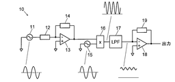
- FIG. 9 shows a basic circuit of the conventional electrical conductivity detector 10.
- the sensor unit 12 is composed of a pair of electrodes arranged with a sample solution interposed therebetween, and a sine wave AC voltage is applied thereto from the AC power source 11.
- a current corresponding to the electrical conductivity of the sample solution existing between the electrodes flows between the electrodes.
- the amplifier 13 generates a voltage signal corresponding to the current flowing through the sensor unit 12, and the magnitude (gain) of the output voltage signal of the amplifier 13 with respect to the magnitude of the current is adjusted by the value of the variable resistor 14 provided in the amplifier 13. Is done.
- the output signal of the amplifier 13 is multiplied by a reference signal (sine wave) having the same frequency and phase as the AC power supply 11 in the multiplier 16.
- the signal output from the multiplication unit 16 has an offset (DC component) proportional to the electrical conductivity of the sample in the sensor unit 12, and the original frequency signal (the signal of the AC power supply 11, the reference signal of the reference signal output unit 15). ) With a cosine wave ripple (alternating current component) that is twice as large. This output signal is passed through a low-pass filter (LPF) 17 to remove ripples, thereby obtaining a signal (DC voltage) representing the electrical conductivity of the sample.
- LPF low-pass filter
- the gain of the amplifier 13 is adjusted by changing the value of the variable resistor 14 so that the output of the amplifier 13 falls within an appropriate range.
- a compensation amplifier 18 is placed after the low-pass filter 17 so that amplification (attenuation) by the amplifier 13 is restored. For example, when the gain of the amplifier 13 is 1 / X times by the variable resistor 14, the gain of the compensation amplifier 18 is X times by the variable resistor 19.
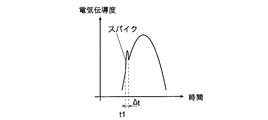
- the low-pass filter 17 sets the time constant ⁇ t to a value sufficiently larger than the cycle of the power supply 11 (about 10 times or more) in order to sufficiently remove the ripple of the AC component. Due to the time constant ⁇ t of the low-pass filter 17, the signal generated according to the change in the sensor unit 12 is delayed in the low-pass filter 17. For this reason, when the gain of the amplifier 13 (value of the variable resistor 14) and the gain of the compensation amplifier 18 (value of the variable resistor 19) are switched simultaneously, the time difference ⁇ t in the output signal of the low-pass filter 17, for example, as shown in FIG. Abnormalities (spikes) depending on In the first place, when the change rate of the electrical conductivity of the sample solution is large, the conventional detection circuit cannot perform detection sufficiently following the change.
- the above-mentioned problem is not limited to the electrical conductivity detector, but relates to a general measuring instrument that continuously measures a physical quantity to be measured by an AC signal.
- the problem to be solved by the present invention is to provide a measuring instrument that can follow a change in a physical quantity to be measured and can also correctly cope with gain switching and the like.
- the measuring device which has been made to solve the above problems, a) a sensor unit that outputs an AC signal having an amplitude corresponding to the physical quantity to be measured; b) a reference signal output unit that outputs a reference signal having the same frequency and the same phase as the AC signal; c) a multiplier for multiplying the AC signal and the reference signal; d) an A / D converter provided before or after the multiplier; e) an integration unit that integrates the digital signal output from the multiplication unit for a predetermined time.
- the A / D conversion unit may perform A / D conversion on the signal (cosine signal) obtained by multiplying both analog signals by the multiplication unit, or the AC output from the sensor unit before the multiplication unit.
- Each of the signal and the reference signal may be A / D converted.
- the multiplication unit also multiplies the digitized signal.
- a basic circuit in the case of the former mode is shown in FIG. 1, and a basic circuit in the case of the latter mode is shown in FIG. In any case, the same reference numerals are assigned to the same elements as those in FIG. 9 which is a conventional basic circuit.
- FIG. 9 is a conventional basic circuit.
- the cosine signal generated by multiplying the output signal of the sensor unit 12 and the reference signal is converted into digital data by the A / D conversion unit 21 and integrated for a predetermined time in the integrating unit 27.
- the output signal and the reference signal of the sensor unit 12 are converted into digital data by the A / D conversion units 31 and 32, and then multiplied by the multiplication unit 36.
- An output is obtained by integrating the multiplication results for a predetermined time.
- the predetermined time is preferably set to 1/2 cycle or 1 cycle of the AC signal in consideration of calculation convenience.
- the sampling period by the A / D conversion unit is sufficiently short and data can be collected to such an extent that the AC signal or the cosine signal that is the multiplication result can be reproduced sufficiently accurately, the time has a predetermined relationship with the period of the AC signal, An integrated value of one cycle or half cycle may be obtained by calculation.
- the value obtained as a result of integration for a predetermined time corresponds to the physical quantity of the measurement target because it corresponds to the amplitude of the AC signal. Therefore, the target physical quantity can be measured with a delay of one cycle of the AC signal. That is, it is possible to follow changes in physical quantities at a much higher speed than when a low-pass filter having a time constant 10 times or more that of a conventional AC signal is used.
- the measuring instrument according to the present invention can include a front-stage amplifier and a rear-stage compensation amplifier as in the conventional case. That is, in the second aspect of the measuring instrument according to the present invention, in addition to the above configuration, a first amplifier is provided between the sensor unit and the multiplication unit, and the inverse of the first amplifier is provided after the integration unit. A second amplifier having a gain (reverse gain) is provided.
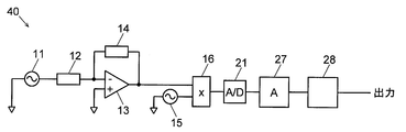
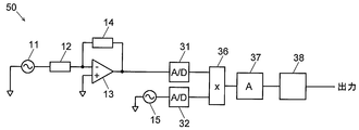
- FIG. 3 shows the amplifier 20 added to the measuring instrument 20 of FIG. 1
- FIG. 4 shows the amplifier added to the measuring instrument 30 of FIG. 3 and 4
- the second amplifiers 28 and 38 are all digital multipliers.
- the measuring instruments 40 and 50 having this configuration, when the AC signal output from the sensor unit 12 is excessive, the first amplifier 13 attenuates it and the second amplifiers 28 and 38 amplify it accordingly. By returning to the original state, it is possible to avoid signal saturation in the A / D converters 21, 31, 32 and the multipliers 16, 36, and to perform correct measurement. At this time, since these measuring instruments 40 and 50 do not use a low-pass filter, it is possible to prevent an abnormality of the output signal due to the time difference of the signal due to the time constant.
- the gain / inverse gain of the first amplifier 13 and the second amplifier 28 and 38 are changed simultaneously, strictly speaking, in many cases, such gain change occurs during the integration for one cycle by the integration units 27 and 37. Arise. In this case, the gain change of the first amplifier 13 takes effect in the middle of the data for one cycle, and the data before amplification (actually attenuation) and the data after amplification (attenuation) are included in the integrated data for one cycle.
- the second amplifiers 28 and 38 amplify the value after integration for one cycle with a reverse gain, the data of that cycle is not accurate and may cause a spike. There is.
- FIG. 5 shows a circuit of a measuring device 60 in which such a memory unit 62 is added to the measuring device 40 of FIG.
- the memory unit 62 always holds the output of the second amplifier 48 (integration result for one cycle of the cosine signal) for each cycle.
- the output of the second amplifier 48 becomes the output of the measuring instrument 60 as it is.
- the gains of the first amplifier 13 and the second amplifier 48 are switched simultaneously, the output of that cycle is taken out from the memory unit 62. Thereby, generation
- the measuring instrument can measure the physical quantity of the object with a slight delay of one cycle of the AC signal. That is, it is possible to follow changes in physical quantities at a much higher speed than when a low-pass filter having a time constant 10 times or more that of a conventional AC signal is used. Further, even when an amplifier / compensation amplifier for gain switching is provided corresponding to a physical quantity having a very large change width, a correct output can be performed quickly corresponding to the gain switching.
- FIG. 3 is a basic circuit diagram in which an A / D conversion unit is provided after a multiplication unit in the measuring device according to the first aspect of the present invention.
- FIG. 3 is a basic circuit diagram in which an A / D conversion unit is provided in front of a multiplication unit in the measuring instrument according to the first aspect of the present invention.
- FIG. 6 is a basic circuit diagram in which an A / D converter is provided after a multiplier in the measuring instrument according to the second aspect of the present invention.
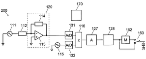
- FIG. 6 is a diagram showing a configuration of an electrical conductivity detector according to an embodiment of the present invention.
- the electrical conductivity detector 100 includes an AC power source 111, a sensor unit 112, a first amplification unit 129, a reference signal output unit 115, a multiplication unit 116, an A / D conversion unit 121, an integration unit 127, The second amplifying unit 128, the memory unit 162, the output selecting unit 163, and the control unit 170 that controls each unit are included.
- the AC power supply 111 uses a voltage source that outputs a sinusoidal AC voltage having a predetermined amplitude and frequency.
- the sensor unit 112 includes a pair of electrodes arranged with an eluate flow path from the ion chromatograph interposed therebetween, and an AC power supply 111 and a first amplification unit 129 are connected to the pair of electrodes.
- the first amplifying unit 129 is an inverting amplifier circuit including an amplifier 113 and a variable resistor 114, and the sensor unit 112 is connected to an inverting input terminal of the amplifier 113.
- the first amplifying unit 129 outputs the current from the sensor unit 112 as a voltage signal amplified by a gain determined by the variable resistor 114.
- the value of the variable resistor 114 is set according to a signal from a gain control unit 172 described later.
- the multiplication unit 116 is a circuit that is connected to the first amplification unit 129 and the reference signal output unit 115 and multiplies and outputs signals input from these, and is configured by an analog multiplication circuit.
- the A / D converter 121 is an analog-digital converter that samples the analog signal input from the multiplier 116 at a predetermined sampling period and converts it into digital data. This sampling period is set sufficiently short with respect to the output frequency of the AC power supply 111.
- the A / D converter 121 has a convertible range (dynamic range) of an input signal, and an upper limit threshold slightly lower than the maximum value and a lower limit threshold slightly higher than the minimum value of the range are controlled respectively. Stored in the unit 170.
- the accumulating unit 127 repeatedly performs processing for accumulating and outputting the digital data input from the A / D converting unit 121 for a time corresponding to a half cycle of the frequency of the AC power supply 111.
- the second amplifying unit 128 is a digital multiplier that multiplies the digital data input from the integrating unit 127 by a predetermined gain and outputs the result.
- the gain of the second amplification unit 128 is set according to a signal from a gain control unit 172 described later.
- the memory unit 162 stores the signal input from the second amplification unit 128 for a predetermined time, and outputs the held signal in accordance with an instruction from the control unit 170 described later.
- the output selection unit 163 connects either the output end of the memory unit 162 or the output end of the second amplifying unit 128 without the memory unit 162 to the output end of the electrical conductivity detector 100.
- the control unit 170 includes an output measurement unit 171, a gain control unit 172, and an output control unit 173.
- the control unit 170 is connected to the first amplification unit 129, the second amplification unit 128, the memory unit 162, and the output selection unit 163 (not shown), and controls each connected unit.
- the output measuring unit 171 monitors the signal at the output terminal of the integrating unit 127 and transmits the measured value to the gain control unit 172.
- This measured value is a DC component proportional to the amplitude of the AC signal output from the first amplifying unit 129.
- the gain control unit 172 stores DC component threshold values (DC upper limit value and DC lower limit value) corresponding to the upper limit threshold value and the lower limit threshold value of the A / D conversion unit 121, and the measured value indicates the DC upper limit value. When it exceeds or falls below the DC lower limit value, a control signal for changing the gain is transmitted to the first amplifying unit 129 so that the subsequent measured value is adjusted to be within the range of the DC lower limit value from the DC upper limit value.
- the gain control unit 172 changes the gain of the second amplification unit 128 simultaneously with the gain change of the first amplification unit 129.
- the gain of the second amplifying unit 128 is set to the inverse of the gain of the first amplifying unit 129.
- the gain control unit 172 notifies the output control unit 173 that the gain has been switched.
- the output control unit 173 controls the output selection unit 163. Before receiving the notification of gain switching, the output control unit 173 connects the output end of the electrical conductivity detector 100 and the output end of the second amplifying unit 128 without going through the memory unit 162. To control. When the output control unit 173 receives the notification, the output control unit 173 transmits a switching signal to the output selection unit 163. In response to this, the output selection unit 163 switches the connection destination of the output end of the electrical conductivity detector 100 from the output end of the second amplification unit 128 to the output end of the memory unit 162. The output control unit 173 transmits a switching signal to the output selection unit 163 after a period of 1 ⁇ 2 cycle of the AC signal from the AC power supply 111 after receiving the notification. In response to this, the output selection unit 163 switches the connection destination of the output end of the electrical conductivity detector 100 from the output end of the memory unit 162 to the output end of the second amplifying unit 128 (not through the memory unit 162).
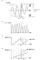
- the AC signal When the AC signal is input to the multiplication unit 116, it is multiplied by the reference signal, and has an offset (DC component) proportional to the electric conductivity of the eluate as shown in FIG. This becomes a cosine signal on which a ripple of a cosine wave twice that of the AC signal is superimposed.
- the cosine signal is converted into digital data by the A / D converter 121.
- the integrating unit 127 integrates the digital data sent from the A / D converting unit 121 every half cycle of the AC signal, that is, every cycle of the cosine signal, and outputs the integrated value. As a result, digital data corresponding to a DC component from which the ripple of the cosine signal has been removed is output for each integration cycle (FIG. 7 (c)).
- the second amplifying unit 128 multiplies the accumulated digital data by the reciprocal 1 / X of the gain of the first amplifying unit 129, so that the value before the digital data is amplified by the gain X of the first amplifying unit 129 is obtained. (Fig. 7 (d)).
- the digital data output from the second amplifying unit 128 is stored in the memory unit 162, but the output terminal of the electrical conductivity detector 100 and the second amplifying unit 128 are connected without going through the memory unit 162 except when the gain is switched. Therefore, the output of the second amplifying unit 128 becomes the output of the electrical conductivity detector 100 as it is.
- the gain control unit 172 changes the gains of the first amplification unit 129 and the second amplification unit 128 when the output of the second amplification unit 128 measured by the output measurement unit 171 exceeds a predetermined DC upper limit value. In the output waveform of the second amplifying unit 128 in FIG. 7C, the output value at the time tc1 exceeds the DC upper limit value.
- the gain control unit 172 transmits a signal for setting the gain of the first amplifying unit 129 to 1/2 the current gain X at time tc1, and the gain of the second amplifying unit 128 is twice the current gain 1 / X. A signal is transmitted.
- the amplitude of the AC signal output from the first amplifying unit 129 after the time tc2 is reduced, and the signal input to the A / D converting unit 121 is A / D. It is within the dynamic range of the conversion unit 121 (FIG. 7A). Note that the magnification for changing the gain may be other than double, and may be appropriately set according to the dynamic range and the expected change rate of the DC signal.
- the integration unit 127 When the gain is switched in the middle of integration by the integration unit 127, the integration unit 127 outputs a value in which data before gain switching and data after switching are mixed in one integration data. Since this digital data is multiplied by the gain after switching, a spike as shown by a broken line in FIG. 7D is generated on the data output from the second amplifying unit 128.
- the output control unit 173 When the output control unit 173 receives a gain switching notification from the gain control unit 172, the output control unit 173 transmits a switching signal to the output selection unit 163. In response to the signal, the output selection unit 163 switches the connection destination of the output end of the electrical conductivity detector 100 to the output end of the memory unit 162, and uses the output of the memory unit 162 as the output of the electrical conductivity detector 100. When the next digital data is output, the output control unit 173 transmits a switching signal to the output control unit 163, and the output selection unit 163 receives the signal, and the output selection unit 163 receives the signal at the output end of the electrical conductivity detector 100. The connection destination is switched to the output terminal of the second amplification unit 128. As described above, a spike is generated in the output of the second amplifying unit 128 immediately after the gain switching, but the spike is prevented from being output by switching the output selecting unit 163, as shown by the solid line in FIG. 7 (d). You can get the output without.
- the gain of the first amplification unit 129 is set to twice the current gain X, and the gain of the second amplification unit 128 is set to 1 / X of the current gain 1 / X.
- the gain can be switched by setting to 2 times and performing other processing in the same manner as in the above embodiment.
- the integration time of the integration unit is set to the time of 1/2 cycle of the AC signal, but it may be longer than this.
- the integration time in this case can be set to an integral multiple of a half period of the AC signal, thereby removing the AC component of the signal.
- the time for the output selection unit to connect the output of the memory unit and the output terminal of the measuring device is set to 1/2 period of the AC signal, but it may be longer.
- the A / D conversion unit may be provided in front of the multiplication unit (FIG. 8).
- the AC signal from the first amplifying unit 129 and the reference signal from the reference signal output unit 115 are respectively converted into digital data by the A / D conversion units 131 and 132 provided before the multiplying unit 116, and multiplied.
- the unit 116 is configured to multiply the digital data.
- Other configurations are the same as in the above embodiment.
Landscapes
- Chemical & Material Sciences (AREA)
- Analytical Chemistry (AREA)
- Physics & Mathematics (AREA)
- Health & Medical Sciences (AREA)
- Life Sciences & Earth Sciences (AREA)
- Biochemistry (AREA)
- General Health & Medical Sciences (AREA)
- General Physics & Mathematics (AREA)
- Immunology (AREA)
- Pathology (AREA)
- Electrochemistry (AREA)
- Chemical Kinetics & Catalysis (AREA)
- Investigating Or Analyzing Materials By The Use Of Electric Means (AREA)
- Measurement Of Resistance Or Impedance (AREA)
Abstract
測定対象の物理量に対応した振幅を有する交流信号を出力するセンサ部12と、前記交流信号と同じ周波数、同じ位相を有する参照信号を出力する参照信号出力部15と、前記交流信号と前記参照信号を乗算する乗算部16と、前記乗算部16の前又は後に置かれたA/D変換部21と、前記乗算部16の出力であるデジタル信号を所定時間だけ積算する積算部37とを有する測定器20を用いることで、測定対象の物理量に対して、わずか交流信号の1周期分の遅れで、その値を測定することができる。
Description
本発明は、イオンクロマトグラフの検出器に用いられる電気伝導度検出器等の、交流信号を用いて物理量を測定する測定器に関する。
イオンクロマトグラフでは、カラムで分離された試料の各成分(イオン)を検出するための検出器として電気伝導度検出器が多く用いられる。電気伝導度検出器は、イオンクロマトグラフからの溶出液(試料液)の流路を挟んで配置された一対の電極の間に電圧を印加し、両電極間を流れる電流を測定することにより両電極間を流れる溶出液の電気伝導度を算出し、イオンクロマトグラフで分離された成分を検出する。ここで、両電極間に印加する電圧を直流とすると電極間に分極が生じて正確な電気伝導度を測定することができないため、電圧には振幅、周波数が一定の交流(例えば、サイン波)が用いられる。
従来の電気伝導度検出器10の基本的回路を図9に示す。センサ部12は試料液を挟んで配置された1対の電極から成り、そこに交流電源11からサイン波状の交流電圧が印加される。これにより、両電極間には両者の間に存在する試料液の電気伝導度に応じた電流が流れる。アンプ13はセンサ部12に流れる電流に応じた電圧信号を生成するが、電流の大きさに対するアンプ13の出力電圧信号の大きさ(ゲイン)はアンプ13に設けられた可変抵抗14の値により調整される。アンプ13の出力信号は乗算部16において交流電源11と同じ周波数、位相を持つ参照信号(サイン波)と乗算される。乗算部16から出力される信号は、センサ部12における試料の電気伝導度に比例したオフセット(直流成分)を持ち、周波数が元の信号(交流電源11の信号、参照信号出力部15の参照信号)の2倍のコサイン波のリップル(交流成分)が重畳した波形を有する。この出力信号をローパスフィルタ(LPF)17に通し、リップルを除去することにより、試料の電気伝導度を表す信号(直流電圧)を得る。
センサ部12を流れる試料液の電気伝導度が非常に大きい場合、両電極間を流れる電流は非常に大きくなり、乗算部16等の後続の回路がそのような過大な信号に対応しきれず出力が飽和してしまう。逆に、試料液の電気伝導度が非常に小さい場合、出力信号はノイズに埋もれてしまう。そこで、可変抵抗14の値を変更することによりアンプ13のゲインを調整し、アンプ13の出力が適度な範囲内に収まるようにする。そして、ローパスフィルタ17の後に補償アンプ18を置き、アンプ13による増幅(減衰)を元に戻すようにしている。例えば、可変抵抗14によりアンプ13のゲインを1/X倍としたとき、可変抵抗19により補償アンプ18のゲインをX倍とする。
上記の検出回路において、ローパスフィルタ17は、交流成分のリップルを十分に除去するため、時定数Δtを、電源11の周期よりも十分大きな(10倍程度以上の)値とする。このローパスフィルタ17の時定数Δtにより、センサ部12における変化に応じて生成された信号は、ローパスフィルタ17において遅延が生じる。このため、アンプ13のゲイン(可変抵抗14の値)と補償アンプ18のゲイン(可変抵抗19の値)を同時に切り替えると、例えば図10に示すように、ローパスフィルタ17の出力信号においてその時間差Δtに応じた異常(スパイク)が生じる。また、そもそも試料液の電気伝導度の変化速度が大きい場合、上記従来の検出回路ではその変化に十分追従した検出が行えない。
上記問題は、電気伝導度検出器に限らず、測定対象の物理量を交流信号により連続的に測定する測定器一般に関わる問題である。
本発明が解決しようとする課題は、測定対象の物理量の変化に追従することが可能であり、かつ、ゲイン切替え等にも正しく対応することが可能な測定器を提供することである。
上記課題を解決するために成された本発明に係る測定器は、
a) 測定対象の物理量に対応した振幅を有する交流信号を出力するセンサ部と、
b) 前記交流信号と同じ周波数、同じ位相を有する参照信号を出力する参照信号出力部と、
c) 前記交流信号と前記参照信号を乗算する乗算部と、
d) 前記乗算部の前又は後に設けられたA/D変換部と、
e) 前記乗算部の出力であるデジタル信号を所定時間だけ積算する積算部と
を有することを特徴とする。
a) 測定対象の物理量に対応した振幅を有する交流信号を出力するセンサ部と、
b) 前記交流信号と同じ周波数、同じ位相を有する参照信号を出力する参照信号出力部と、
c) 前記交流信号と前記参照信号を乗算する乗算部と、
d) 前記乗算部の前又は後に設けられたA/D変換部と、
e) 前記乗算部の出力であるデジタル信号を所定時間だけ積算する積算部と
を有することを特徴とする。
上記測定器においてA/D変換部は、乗算部で両アナログ信号が乗算された後の信号(コサイン信号)をA/D変換してもよいし、乗算部の前でセンサ部の出力する交流信号と参照信号をそれぞれA/D変換してもよい。後者の場合は、乗算部もデジタル化された信号を乗算する。前者の態様の場合の基本的な回路を図1に、後者の態様の場合の基本的な回路を図2に示す。いずれにおいても、従来の基本的な回路である図9と同じ要素には同じ番号を付した。図1の測定器20では、センサ部12の出力信号と参照信号との乗算により生成されたコサイン信号はA/D変換部21によりデジタルデータに変換され、積算部27において所定の時間だけ積算され出力される。また、図2の測定器30では、センサ部12の出力信号と参照信号はそれぞれのA/D変換部31、32によりデジタルデータに変換された後、乗算部36において乗算される。この乗算結果を所定の時間だけ積算したものが出力となる。この所定の時間としては、計算の便を考慮すると前記交流信号の1/2周期又は1周期とするのが望ましい。A/D変換部によるサンプリング周期が十分短く、交流信号又はその乗算結果であるコサイン信号が十分精密に再現できる程度にデータを採取できる場合は、交流信号の周期と所定の関係を持つ時間とし、計算により1周期又は1/2周期の積算値を求めてもよい。
図1及び図2に示す態様の測定器20、30では、所定の時間だけ積算された結果の値は、該交流信号の振幅に対応することから、測定対象の物理量に対応する。従って、わずか交流信号の1周期分の遅れで対象の物理量を測定することができる。すなわち、従来の交流信号の10倍以上の時定数のローパスフィルタを用いていた場合よりも遙かに高速で物理量の変化に追従することができる。
測定対象の物理量の変化の幅が非常に大きい場合、前記A/D変換部21、31、32の変換可能範囲(ダイナミックレンジ)を超える可能性がある。そのような場合には、本発明に係る測定器は、従来と同様に前段のアンプ及び後段の補償アンプを備えることができる。すなわち、本発明に係る測定器の第2の態様のものは、上記構成に加えて、前記センサ部と前記乗算部の間に第1アンプを、前記積算部の後に該第1アンプの逆数のゲイン(逆ゲイン)を有する第2アンプをそれぞれ備える。図1の測定器20にそれらアンプを付加したものを図3に、図2の測定器30にそれらを付加したものを図4に示す。図3及び図4の測定器40、50において、第2アンプ28、38はいずれもデジタル乗算器となる。
この構成の測定器40、50では、センサ部12の出力する交流信号が過大である場合には、第1アンプ13によりそれを減衰し、その分だけ第2アンプ28、38でそれを増幅して元に戻すことにより、A/D変換部21、31、32や乗算部16、36における信号の飽和を避け、正しい測定を行うことができる。このとき、これら測定器40、50ではローパスフィルタを用いないため、その時定数による信号の時間差に起因する出力信号の異常を防止することができる。なお、センサ部12の出力する交流信号が過小であってノイズに対して十分な強度が確保できない場合(十分なS/N比が得られない場合)には、逆に、第1アンプ13において交流信号を増幅し、その分だけ第2アンプ28、38で減衰して元に戻す。
交流信号の振幅が前記変換可能範囲を考慮して設定された所定の閾値を超えた時点で(或いは、前記十分なS/N比を考慮して設定された所定の閾値を下回った時点で)第1アンプ13と第2アンプ28、38のゲイン/逆ゲインを同時に変化させると、厳密には、多くの場合、積算部27、37による1周期分の積算の途中でそのようなゲイン変化が生じる。この場合、第1アンプ13のゲイン変化は1周期分のデータの途中で発効し、1周期分の積算データの中に増幅(実際には減衰)前のデータと増幅(減衰)後のデータが混在することになるのに対し、第2アンプ28、38は1周期分の積算後の値を逆ゲインで増幅するため、その周期のデータは正確なものとはならず、スパイクが生じる可能性がある。
この場合のスパイクも補償するために、本発明に係る測定器は、上記構成に加えて、前記乗算部の出力であるデジタルデータを、少なくとも前記交流信号の1周期の時間だけ逐次保存するメモリ部を備えるようにしてもよい。図3の測定器40にこのようなメモリ部62を付加した測定器60の回路を図5に示す。この測定器60では、メモリ部62には常に第2アンプ48の出力(コサイン信号の1周期分の積算結果)を周期毎に保持しておく。通常は第2アンプ48の出力がそのまま測定器60の出力となるが、第1アンプ13及び第2アンプ48のゲインを同時に切り替えたときは、その周期の出力をメモリ部62から取り出す。これにより、スパイクの発生を防止することができる。
本発明に係る測定器は、わずか交流信号の1周期分の遅れで対象の物理量を測定することができる。すなわち、従来の交流信号の10倍以上の時定数のローパスフィルタを用いていた場合よりも遙かに高速で物理量の変化に追従することができる。また、変化の幅が非常に大きい物理量に対応して、ゲイン切り替えのためのアンプ・補償アンプを設けた場合においても、それらのゲイン切り替えに素早く対応して正しい出力を行うことができる。
本発明に係る測定器の実施形態について図面を参照しつつ説明する。以下の実施形態では、イオンクロマトグラフに用いられる電気伝導度検出器を例に挙げて説明する。
図6は本発明の一実施形態に係る電気伝導度検出器の構成を示す図である。電気伝導度検出器100は、交流電源111と、センサ部112と、第1増幅部129と、参照信号出力部115と、乗算部116と、A/D変換部121と、積算部127と、第2増幅部128と、メモリ部162と、出力選択部163と、各部を制御する制御部170を有する。
交流電源111には、所定の振幅、周波数のサイン波状の交流電圧を出力する電圧源を用いる。センサ部112はイオンクロマトグラフからの溶出液の流路を挟んで配置された一対の電極から成り、該一対の電極に交流電源111及び第1増幅部129が接続されている。
第1増幅部129は、アンプ113と、可変抵抗114で構成された反転増幅回路であり、アンプ113の反転入力端子に前記センサ部112が接続され。第1増幅部129は、センサ部112からの電流を可変抵抗114により定まるゲインで増幅した電圧信号として出力する。可変抵抗114の値は、後述のゲイン制御部172からの信号に応じて設定される。
乗算部116は、第1増幅部129と参照信号出力部115にそれぞれ接続され、これらから入力される信号を乗算して出力する回路であり、アナログ乗算回路で構成される。
A/D変換部121は、乗算部116から入力されるアナログ信号を所定のサンプリング周期でサンプリングしてデジタルデータに変換するアナログ-デジタル変換器である。このサンプリング周期は交流電源111の出力周波数に対して十分短く設定されている。A/D変換部121には入力される信号の変換可能範囲(ダイナミックレンジ)があり、この最大値よりもわずかに低い上限閾値と、該範囲の最小値よりもわずかに高い下限閾値がそれぞれ制御部170内に保存される。
積算部127は、A/D変換部121から入力されるデジタルデータを交流電源111の周波数の1/2周期分の時間だけ積算して出力する処理を繰り返し行う。
第2増幅部128は、積算部127から入力されるデジタルデータに所定のゲインを乗算して出力するデジタル乗算器である。第2増幅部128のゲインは、後述のゲイン制御部172からの信号に応じて設定される。
メモリ部162は、第2増幅部128から入力される信号を所定時間だけ保存し、後述の制御部170の指示に応じて該保持した信号を出力する。出力選択部163は、メモリ部162の出力端又はメモリ部162を介在しない第2増幅部128の出力端のいずれか一方を電気伝導度検出器100の出力端に接続する。
制御部170は、出力測定部171と、ゲイン制御部172と、出力制御部173から構成される。制御部170は、第1増幅部129と第2増幅部128、メモリ部162、出力選択部163に接続されており(図示略)、接続された各部の制御を行う。
出力測定部171は、積算部127の出力端における信号をモニタし、その測定値をゲイン制御部172に送信する。この測定値は第1増幅部129から出力される交流信号の振幅に比例した直流成分である。ゲイン制御部172には、A/D変換部121の前記上限閾値と下限閾値に対応した直流成分の閾値(直流上限値、直流下限値)が保存されており、前記測定値が直流上限値を超え、又は直流下限値を下回った場合に第1増幅部129にゲイン変更の制御信号を送信することで、以降の測定値が直流上限値から直流下限値の範囲内となるように調整する。また、ゲイン制御部172は、第1増幅部129のゲイン変更と同時に、第2増幅部128のゲインを変更する。第2増幅部128のゲインには、第1増幅部129のゲインの逆数が設定される。ゲイン制御部172は、ゲインの切り替えを行ったことを出力制御部173に通知する。
出力制御部173は出力選択部163を制御する。出力制御部173は前記ゲインの切り替えの通知を受け取る前は、メモリ部162を介さずに電気伝導度検出器100の出力端と第2増幅部128の出力端を接続するよう、出力選択部163を制御する。そして出力制御部173は、前記通知を受け取ると、出力選択部163に切り替え信号を送信する。それを受けて出力選択部163は、電気伝導度検出器100の出力端の接続先を第2増幅部128の出力端からメモリ部162の出力端に切り替える。出力制御部173は、前記通知を受け取ってから交流電源111からの交流信号の1/2周期の時間だけ後に出力選択部163に切り替え信号を送信する。それを受けて出力選択部163は、電気伝導度検出器100の出力端の接続先をメモリ部162の出力端から(メモリ部162を介さない)第2増幅部128の出力端に切り替える。
次に本実施形態に係る電気伝導度検出器の動作を説明する。まず、前記交流信号がA/D変換器121のダイナミックレンジの範囲内で変化している場合の動作について説明する。
交流電源111からセンサ部112に交流電圧が印加されると、センサ部112の電極間に前記溶出液の電気伝導度に応じた振幅の交流電流が流れる。この交流電流は第1増幅部129に入力され、第1増幅部129に設定されたゲインXに応じて増幅された交流信号となる(図7(a)の1周期目)。
前記交流信号が乗算部116に入力されると、参照信号と乗算されて、図7(b)に示すように、前記溶出液の電気伝導度に比例したオフセット(直流成分)を持ち、周波数が前記交流信号の2倍のコサイン波のリップルが重畳したコサイン信号となる。そして該コサイン信号がA/D変換部121によりデジタルデータに変換される。
積算部127はA/D変換部121から送られるデジタルデータを前記交流信号の1/2周期、すなわちコサイン信号の1周期毎に積算を行い、その積算値を出力する。これによりコサイン信号のリップルが除去された直流成分に相当するデジタルデータが積算の周期毎に出力される(図7(c))。
第2増幅部128は積算されたデジタルデータに、第1増幅部129のゲインの逆数1/Xを乗算することで、該デジタルデータを第1増幅部129のゲインXで増幅される前の値に戻す(図7(d))。
第2増幅部128から出力されたデジタルデータはメモリ部162に保存されるが、ゲイン切り替え時以外はメモリ部162を介さずに電気伝導度検出器100の出力端と第2増幅部128が接続される設定であるため、第2増幅部128の出力がそのまま電気伝導度検出器100の出力となる。
次に前記交流信号がA/D変換器121の前記上限閾値を超えた場合の第1増幅部129及び第2増幅部の128のゲインの切り替え動作について説明する。
ゲイン制御部172は、出力測定部171で測定した第2増幅部128の出力が所定の直流上限値を超えた場合に第1増幅部129及び第2増幅部128のゲインの変更を行う。図7(c)の第2増幅部128の出力波形では、時刻tc1の出力値が直流上限値を超えている。ゲイン制御部172は時刻tc1において第1増幅部129のゲインを現在のゲインXの1/2倍とする信号を送信するとともに、第2増幅部128のゲインを現在のゲイン1/Xの2倍とする信号を送信する。両増幅部のゲインが時刻tc2において切り替えられると、該時刻tc2以降の第1増幅部129から出力される交流信号の振幅は小さくなり、A/D変換部121へ入力される信号がA/D変換部121のダイナミックレンジの範囲内となる(図7(a))。なお、ゲインを変更する倍率は2倍以外でもよく、ダイナミックレンジや予想される直流信号の変化速度に応じて適宜設定してもよい。
上記ゲインは積算部127による積算の途中で切り替えられると、1つの積算データの中にゲイン切り替え前のデータと切り替え後のデータが混在した値が積算部127から出力される。このデジタルデータには、切り替え後のゲインが乗算されるため、第2増幅部128から出力されるデータ上に、図7(d)の破線で示すようなスパイクが生じることとなる。
出力制御部173は、ゲイン制御部172からゲインの切り替えの通知を受け取ると、出力選択部163に切り替え信号を送信する。該信号を受けて、出力選択部163は電気伝導度検出器100の出力端の接続先をメモリ部162の出力端に切り替え、メモリ部162の出力を電気伝導度検出器100の出力とする。そして、次のデジタルデータを出力する際には、出力制御部173は出力制御部163に切り替え信号を送信し、該信号を受けて、出力選択部163は電気伝導度検出器100の出力端の接続先を第2増幅部128の出力端に切り替える。前述のとおりゲイン切り替え直後の第2増幅部128の出力にはスパイクが生じるが、出力選択部163を切り替えることでスパイクが出力されることを防ぎ、図7(d)の実線で示すようなスパイクのない出力を得ることができる。
電気伝導度が時間とともに減少し、下限値を下回った場合についても第1増幅部129のゲインを現在のゲインXの2倍、第2増幅部128のゲインを現在のゲイン1/Xの1/2倍に設定し、その他の処理を上記実施形態と同様に行うことでにゲインの切り替えを行うことができる。
なお、上記実施形態は一例であって、本発明の趣旨に従って適宜変形や修正を行えることは明らかである。例えば、上記実施形態では、積算部の積算時間を交流信号の1/2周期の時間としたが、これよりも長くしてもよい。この場合の積算時間は、交流信号の1/2周期の整数倍に設定することで、信号の交流成分を除去できる。また、出力選択部がメモリ部の出力と測定器の出力端を接続する時間を交流信号の1/2周期分としたが、これより長い時間としてもよい。
また、A/D変換部を乗算部の前に設けた構成としてもよい(図8)。この変形例では乗算部116の前に設けたA/D変換部131、132により第1増幅部129からの交流信号と、参照信号出力部115からの参照信号をそれぞれデジタルデータに変換し、乗算部116がこれらのデジタルデータを乗算する構成である。これ以外の構成は上記実施形態と同様である。
10、100、200…電気伝導度検出器
11、111…交流電源
12、112…センサ部
13、28、38、113、128…アンプ
14、19、114…可変抵抗
15、115…参照信号出力部
16、36、116、136…乗算部
17…ローパスフィルタ
20、30、40、50、60…測定器
21、31、32、121、131、132…A/D変換部
27、37、127…積算部
62、162…メモリ部
63、163…出力選択部
129…第1増幅部
170…制御部
171…出力測定部
172…ゲイン制御部
173…出力制御部
11、111…交流電源
12、112…センサ部
13、28、38、113、128…アンプ
14、19、114…可変抵抗
15、115…参照信号出力部
16、36、116、136…乗算部
17…ローパスフィルタ
20、30、40、50、60…測定器
21、31、32、121、131、132…A/D変換部
27、37、127…積算部
62、162…メモリ部
63、163…出力選択部
129…第1増幅部
170…制御部
171…出力測定部
172…ゲイン制御部
173…出力制御部
Claims (3)
- a) 測定対象の物理量に対応した振幅を有する交流信号を出力するセンサ部と、
b) 前記交流信号と同じ周波数、同じ位相を有する参照信号を出力する参照信号出力部と、
c) 前記交流信号と前記参照信号を乗算する乗算部と、
d) 前記乗算部の前又は後に設けられたA/D変換部と、
e) 前記乗算部の出力であるデジタル信号を所定時間だけ積算する積算部と
を有することを特徴とする測定器。 - 更に、
f) 前記センサ部と前記乗算部の間に設けられた第1アンプと、
g) 前記積算部の後に設けられ、前記第1アンプの逆数のゲインを有する第2アンプと
を有することを特徴とする請求項1に記載の測定器。 - 更に、
h) 前記乗算部の出力であるデジタルデータを、少なくとも前記交流信号の1/2周期の時間だけ逐次保存するメモリ部
を有することを特徴とする請求項1に記載の測定器。
Priority Applications (3)
| Application Number | Priority Date | Filing Date | Title |
|---|---|---|---|
| US16/304,188 US11204341B2 (en) | 2016-05-31 | 2017-03-14 | Measuring instrument |
| CN201780032749.6A CN109196344B (zh) | 2016-05-31 | 2017-03-14 | 电导率检测器 |
| JP2018520671A JP6631705B2 (ja) | 2016-05-31 | 2017-03-14 | 電気伝導度検出器 |
Applications Claiming Priority (2)
| Application Number | Priority Date | Filing Date | Title |
|---|---|---|---|
| JP2016-108873 | 2016-05-31 | ||
| JP2016108873 | 2016-05-31 |
Publications (1)
| Publication Number | Publication Date |
|---|---|
| WO2017208561A1 true WO2017208561A1 (ja) | 2017-12-07 |
Family
ID=60479278
Family Applications (1)
| Application Number | Title | Priority Date | Filing Date |
|---|---|---|---|
| PCT/JP2017/010095 Ceased WO2017208561A1 (ja) | 2016-05-31 | 2017-03-14 | 測定器 |
Country Status (4)
| Country | Link |
|---|---|
| US (1) | US11204341B2 (ja) |
| JP (1) | JP6631705B2 (ja) |
| CN (1) | CN109196344B (ja) |
| WO (1) | WO2017208561A1 (ja) |
Cited By (1)
| Publication number | Priority date | Publication date | Assignee | Title |
|---|---|---|---|---|
| CN112470109A (zh) * | 2018-09-07 | 2021-03-09 | 阿尔卑斯阿尔派株式会社 | 传感器装置和其控制方法以及程序 |
Families Citing this family (2)
| Publication number | Priority date | Publication date | Assignee | Title |
|---|---|---|---|---|
| WO2019155592A1 (ja) * | 2018-02-09 | 2019-08-15 | 株式会社島津製作所 | 電気伝導度検出器及びバックグランド減算信号の位相調整値を求めるための方法 |
| US11469088B2 (en) | 2020-10-19 | 2022-10-11 | Thermo Finnigan Llc | Methods and apparatus of adaptive and automatic adjusting and controlling for optimized electrometer analog signal linearity, sensitivity, and range |
Citations (6)
| Publication number | Priority date | Publication date | Assignee | Title |
|---|---|---|---|---|
| JPS57166550A (en) * | 1981-04-07 | 1982-10-14 | Auburn Int | Method of measuring liquid content of fluid of mixed phase in container |
| JPS62167456A (ja) * | 1985-11-30 | 1987-07-23 | Shimadzu Corp | 電気伝導度検出器 |
| JPH02108979A (ja) * | 1988-10-19 | 1990-04-20 | Hitachi Ltd | 電気伝導度検出器 |
| JPH08129000A (ja) * | 1994-10-31 | 1996-05-21 | Shimadzu Corp | 電気伝導度検出器 |
| JP2006112490A (ja) * | 2004-10-13 | 2006-04-27 | Boc Edwards Kk | 磁気軸受装置 |
| JP2016099207A (ja) * | 2014-11-20 | 2016-05-30 | パナソニックIpマネジメント株式会社 | 電圧測定装置 |
Family Cites Families (6)
| Publication number | Priority date | Publication date | Assignee | Title |
|---|---|---|---|---|
| WO2001075428A1 (en) * | 2000-03-30 | 2001-10-11 | Organo Corporation | Ion concentration meter |
| CN2580438Y (zh) * | 2002-04-29 | 2003-10-15 | 长春工业大学 | 电导率测量仪 |
| JP4394409B2 (ja) * | 2003-09-25 | 2010-01-06 | 株式会社日立国際電気 | プリディストーション方式歪補償機能付き増幅器 |
| CN1540463A (zh) * | 2003-10-31 | 2004-10-27 | 广州威纳电子科技有限公司 | 带水电导率检测的饮水机电脑控制器 |
| CN101609058B (zh) * | 2009-07-23 | 2012-11-14 | 中国农业大学 | 一种土壤电导率测量装置和方法 |
| CN102116756B (zh) * | 2009-12-30 | 2014-11-05 | 上海城投原水有限公司 | 一种基于单片机的液体电导率测量方法 |
-
2017
- 2017-03-14 WO PCT/JP2017/010095 patent/WO2017208561A1/ja not_active Ceased
- 2017-03-14 CN CN201780032749.6A patent/CN109196344B/zh active Active
- 2017-03-14 US US16/304,188 patent/US11204341B2/en active Active
- 2017-03-14 JP JP2018520671A patent/JP6631705B2/ja active Active
Patent Citations (6)
| Publication number | Priority date | Publication date | Assignee | Title |
|---|---|---|---|---|
| JPS57166550A (en) * | 1981-04-07 | 1982-10-14 | Auburn Int | Method of measuring liquid content of fluid of mixed phase in container |
| JPS62167456A (ja) * | 1985-11-30 | 1987-07-23 | Shimadzu Corp | 電気伝導度検出器 |
| JPH02108979A (ja) * | 1988-10-19 | 1990-04-20 | Hitachi Ltd | 電気伝導度検出器 |
| JPH08129000A (ja) * | 1994-10-31 | 1996-05-21 | Shimadzu Corp | 電気伝導度検出器 |
| JP2006112490A (ja) * | 2004-10-13 | 2006-04-27 | Boc Edwards Kk | 磁気軸受装置 |
| JP2016099207A (ja) * | 2014-11-20 | 2016-05-30 | パナソニックIpマネジメント株式会社 | 電圧測定装置 |
Cited By (2)
| Publication number | Priority date | Publication date | Assignee | Title |
|---|---|---|---|---|
| CN112470109A (zh) * | 2018-09-07 | 2021-03-09 | 阿尔卑斯阿尔派株式会社 | 传感器装置和其控制方法以及程序 |
| CN112470109B (zh) * | 2018-09-07 | 2024-05-28 | 阿尔卑斯阿尔派株式会社 | 传感器装置和其控制方法以及程序 |
Also Published As
| Publication number | Publication date |
|---|---|
| JP6631705B2 (ja) | 2020-01-15 |
| CN109196344A (zh) | 2019-01-11 |
| US11204341B2 (en) | 2021-12-21 |
| CN109196344B (zh) | 2021-05-28 |
| JPWO2017208561A1 (ja) | 2018-10-18 |
| US20200319147A1 (en) | 2020-10-08 |
Similar Documents
| Publication | Publication Date | Title |
|---|---|---|
| JP6631705B2 (ja) | 電気伝導度検出器 | |
| WO1999028756A1 (en) | Method of measuring current while applying a voltage and apparatus therefor | |
| JP5489331B2 (ja) | 電力計測装置 | |
| JPS5875074A (ja) | 容量あるいは他のパラメ−タの測定装置 | |
| CN100462725C (zh) | 用于计量电功率的计量仪 | |
| JP5462062B2 (ja) | 電磁流量計 | |
| US8174254B2 (en) | Measuring device with negative-feedback DC voltage amplifier | |
| US20150219590A1 (en) | Air-fuel ratio detection device | |
| TWI726221B (zh) | 電傳導度檢測器以及求相位調整值的方法 | |
| JP4851363B2 (ja) | インピーダンス測定装置 | |
| KR101399893B1 (ko) | 신호 계측 방법 및 신호 계측 장치 | |
| JP2015105928A (ja) | インピーダンス測定装置及びインピーダンス測定方法 | |
| JPH088747A (ja) | アナログ/デジタル変換回路 | |
| JP4451415B2 (ja) | 電流/電圧変換回路 | |
| JP3355828B2 (ja) | 電気伝導度検出器 | |
| JP2025015927A (ja) | 電気伝導度検出器 | |
| JP4511717B2 (ja) | 電流電圧測定装置 | |
| JP2007132778A (ja) | インピーダンス測定装置 | |
| CN110392821A (zh) | 操作磁感应流量计的方法及磁感应流量计 | |
| RU2331897C2 (ru) | Способ определения напряжения нейтрали и положения нулевой точки | |
| KR20160071841A (ko) | 전력 변환 장치 | |
| JP2004356874A (ja) | センサ入力装置 | |
| JPWO2015145675A1 (ja) | 電圧信号検出装置および電圧信号調整方法 | |
| JP2020144017A (ja) | フィードバック制御システム、フィーバック制御システムを含んだ計測装置 | |
| JP2020169859A (ja) | 測定装置 |
Legal Events
| Date | Code | Title | Description |
|---|---|---|---|
| ENP | Entry into the national phase |
Ref document number: 2018520671 Country of ref document: JP Kind code of ref document: A |
|
| 121 | Ep: the epo has been informed by wipo that ep was designated in this application |
Ref document number: 17806123 Country of ref document: EP Kind code of ref document: A1 |
|
| NENP | Non-entry into the national phase |
Ref country code: DE |
|
| 122 | Ep: pct application non-entry in european phase |
Ref document number: 17806123 Country of ref document: EP Kind code of ref document: A1 |