WO2017208535A1 - 窒化物半導体紫外線発光装置及びその製造方法 - Google Patents
窒化物半導体紫外線発光装置及びその製造方法 Download PDFInfo
- Publication number
- WO2017208535A1 WO2017208535A1 PCT/JP2017/007342 JP2017007342W WO2017208535A1 WO 2017208535 A1 WO2017208535 A1 WO 2017208535A1 JP 2017007342 W JP2017007342 W JP 2017007342W WO 2017208535 A1 WO2017208535 A1 WO 2017208535A1
- Authority
- WO
- WIPO (PCT)
- Prior art keywords
- light emitting
- sapphire substrate
- ultraviolet light
- nitride semiconductor
- semiconductor ultraviolet
- Prior art date
- Legal status (The legal status is an assumption and is not a legal conclusion. Google has not performed a legal analysis and makes no representation as to the accuracy of the status listed.)
- Ceased
Links
Images


Classifications
-
- H—ELECTRICITY
- H10—SEMICONDUCTOR DEVICES; ELECTRIC SOLID-STATE DEVICES NOT OTHERWISE PROVIDED FOR
- H10H—INORGANIC LIGHT-EMITTING SEMICONDUCTOR DEVICES HAVING POTENTIAL BARRIERS
- H10H20/00—Individual inorganic light-emitting semiconductor devices having potential barriers, e.g. light-emitting diodes [LED]
- H10H20/80—Constructional details
- H10H20/81—Bodies
- H10H20/819—Bodies characterised by their shape, e.g. curved or truncated substrates
- H10H20/82—Roughened surfaces, e.g. at the interface between epitaxial layers
-
- H—ELECTRICITY
- H10—SEMICONDUCTOR DEVICES; ELECTRIC SOLID-STATE DEVICES NOT OTHERWISE PROVIDED FOR
- H10H—INORGANIC LIGHT-EMITTING SEMICONDUCTOR DEVICES HAVING POTENTIAL BARRIERS
- H10H20/00—Individual inorganic light-emitting semiconductor devices having potential barriers, e.g. light-emitting diodes [LED]
- H10H20/01—Manufacture or treatment
-
- H—ELECTRICITY
- H10—SEMICONDUCTOR DEVICES; ELECTRIC SOLID-STATE DEVICES NOT OTHERWISE PROVIDED FOR
- H10H—INORGANIC LIGHT-EMITTING SEMICONDUCTOR DEVICES HAVING POTENTIAL BARRIERS
- H10H20/00—Individual inorganic light-emitting semiconductor devices having potential barriers, e.g. light-emitting diodes [LED]
- H10H20/80—Constructional details
- H10H20/81—Bodies
- H10H20/822—Materials of the light-emitting regions
- H10H20/824—Materials of the light-emitting regions comprising only Group III-V materials, e.g. GaP
- H10H20/825—Materials of the light-emitting regions comprising only Group III-V materials, e.g. GaP containing nitrogen, e.g. GaN
-
- H—ELECTRICITY
- H10—SEMICONDUCTOR DEVICES; ELECTRIC SOLID-STATE DEVICES NOT OTHERWISE PROVIDED FOR
- H10H—INORGANIC LIGHT-EMITTING SEMICONDUCTOR DEVICES HAVING POTENTIAL BARRIERS
- H10H20/00—Individual inorganic light-emitting semiconductor devices having potential barriers, e.g. light-emitting diodes [LED]
- H10H20/80—Constructional details
- H10H20/85—Packages
- H10H20/852—Encapsulations
- H10H20/854—Encapsulations characterised by their material, e.g. epoxy or silicone resins
-
- H—ELECTRICITY
- H10—SEMICONDUCTOR DEVICES; ELECTRIC SOLID-STATE DEVICES NOT OTHERWISE PROVIDED FOR
- H10H—INORGANIC LIGHT-EMITTING SEMICONDUCTOR DEVICES HAVING POTENTIAL BARRIERS
- H10H20/00—Individual inorganic light-emitting semiconductor devices having potential barriers, e.g. light-emitting diodes [LED]
- H10H20/01—Manufacture or treatment
- H10H20/036—Manufacture or treatment of packages
- H10H20/0362—Manufacture or treatment of packages of encapsulations
-
- H—ELECTRICITY
- H10—SEMICONDUCTOR DEVICES; ELECTRIC SOLID-STATE DEVICES NOT OTHERWISE PROVIDED FOR
- H10H—INORGANIC LIGHT-EMITTING SEMICONDUCTOR DEVICES HAVING POTENTIAL BARRIERS
- H10H20/00—Individual inorganic light-emitting semiconductor devices having potential barriers, e.g. light-emitting diodes [LED]
- H10H20/80—Constructional details
- H10H20/85—Packages
- H10H20/852—Encapsulations
- H10H20/853—Encapsulations characterised by their shape
-
- H—ELECTRICITY
- H10—SEMICONDUCTOR DEVICES; ELECTRIC SOLID-STATE DEVICES NOT OTHERWISE PROVIDED FOR
- H10H—INORGANIC LIGHT-EMITTING SEMICONDUCTOR DEVICES HAVING POTENTIAL BARRIERS
- H10H20/00—Individual inorganic light-emitting semiconductor devices having potential barriers, e.g. light-emitting diodes [LED]
- H10H20/80—Constructional details
- H10H20/85—Packages
- H10H20/857—Interconnections, e.g. lead-frames, bond wires or solder balls
Definitions
- the present invention relates to a nitride semiconductor ultraviolet light-emitting device, and more particularly to a back-emission nitride semiconductor ultraviolet light-emitting device that takes out light having an emission center wavelength of about 350 nm or less sealed with an amorphous fluororesin from the back side of the substrate. .
- Non-Patent Document 1 Non-Patent Document 1
- Non-Patent Document 2 Non-Patent Document 2
- the nitride semiconductor layer is represented by the general formula Al 1-xy Ga x In y N (0 ⁇ x ⁇ 1, 0 ⁇ y ⁇ 1, 0 ⁇ x + y ⁇ 1).
- the light-emitting element structure includes a single quantum well structure (SQW: Single-Quantum-Well) or a multiple quantum well structure (MQW) between an n-type nitride semiconductor layer and a p-type nitride semiconductor layer. ) Having a double heterostructure sandwiched between active layers made of nitride semiconductor layers.
- the active layer is an AlGaN-based semiconductor layer
- AlN molar fraction also referred to as Al composition ratio
- an ultraviolet light emitting element having an emission wavelength of about 200 nm to about 365 nm can be obtained.
- a forward current flows from the p-type nitride semiconductor layer toward the n-type nitride semiconductor layer, light emission corresponding to the band gap energy occurs in the active layer.
- flip-chip mounting is generally employed as a mounting form of the nitride semiconductor ultraviolet light-emitting element (see, for example, FIG. 4 in Patent Document 1 below).
- light emitted from the active layer passes through an AlGaN nitride semiconductor and a sapphire substrate having a band gap energy larger than that of the active layer, and is extracted outside the device.
- the sapphire substrate faces upward, the p-side and n-side electrode surfaces formed toward the upper surface of the chip face downward, and each chip-side electrode surface and a package such as a submount
- the electrode pads on the component side are electrically and physically bonded via metal bumps formed on each electrode surface.
- nitride semiconductor ultraviolet light-emitting elements include fluororesins as disclosed in FIGS. 4, 6 and 7 of Patent Document 2 below, or FIGS.
- an ultraviolet light transmissive resin such as a silicone resin and is put to practical use.
- the sealing resin protects the internal ultraviolet light-emitting element from the external atmosphere and prevents the light-emitting element from being deteriorated due to moisture intrusion or oxidation.
- the sealing resin alleviates the light reflection loss caused by the difference in refractive index between the condenser lens and the ultraviolet light emitting element or the difference in refractive index between the ultraviolet irradiation target space and the ultraviolet light emitting element.
- the surface of the sealing resin can be formed into a light-collecting curved surface such as a spherical surface to increase the irradiation efficiency.
- sealing resins for ultraviolet light-emitting elements.
- silicone resins deteriorate when exposed to a large amount of high-energy ultraviolet rays. Yes.
- ultraviolet light emitting devices are being reduced in wavelength and increased in output, tending to accelerate deterioration due to ultraviolet exposure, and increase in power consumption due to increased output increases heat generation. Deterioration of the sealing resin due to heat generation is also a problem.
- Fluorine-based resins are known to have excellent heat resistance and high UV resistance, but general fluorine resins such as polytetrafluoroethylene are opaque. Since the fluororesin has a linear and rigid polymer chain and is easily crystallized, a crystalline part and an amorphous part are mixed, and light is scattered at the interface to become opaque.
- amorphous fluororesins include those obtained by copolymerizing a crystalline polymer fluororesin and making it amorphous as a polymer alloy, or a perfluorodioxole copolymer (trade name Teflon AF manufactured by DuPont). (Registered trademark)) and cyclized polymers of perfluorobutenyl vinyl ether (trade name Cytop (registered trademark) manufactured by Asahi Glass Co., Ltd.).
- the latter cyclized polymer fluororesin has a cyclic structure in the main chain, and therefore tends to be amorphous and has high transparency.
- Amorphous fluororesin can be broadly divided into a binding amorphous fluororesin having a reactive functional group capable of binding to a metal such as a carboxyl group and a hard bond to a metal such as a perfluoroalkyl group.
- a binding amorphous fluororesin having a reactive functional group whose terminal functional group exhibits a binding property to a metal has a depth of emission center wavelength of 300 nm or less.
- ultraviolet light is emitted by applying a forward voltage between the metal electrode wirings connected to the p electrode and the n electrode of the ultraviolet light emitting element, respectively. It has been reported that when the operation is performed, the electrical characteristics of the ultraviolet light emitting element deteriorate.
- a resistive leakage current path is formed between the p-electrode and the n-electrode of the ultraviolet light-emitting element.
- the amorphous fluororesin is a binding amorphous fluororesin
- the binding amorphous fluororesin irradiated with high energy deep ultraviolet rays is subjected to a photochemical reaction. It is considered that the reactive terminal functional group is separated and radicalized to cause a coordinate bond with the metal atom constituting the pad electrode, and the metal atom is separated from the pad electrode.
- Non-Patent Document 3 when a bondable amorphous fluororesin is used and the stress due to the deep ultraviolet light emission operation is continuously applied, the amorphous fluororesin is decomposed by a photochemical reaction. It has been reported that bubbles are generated between the amorphous fluororesin covering the base-side metal electrode wiring and the metal electrode wiring.
- the non-bonding amorphous fluororesin exhibits difficulty bonding to a metal, but when flip-chip mounting, the back surface of the sapphire substrate that is in direct contact with the non-bonding amorphous fluororesin and It also exhibits difficulty bonding to the side surface.
- the bond due to van der Waals force at the interface between the non-bonding amorphous fluororesin and the back surface and side surface of the sapphire substrate is weak, a repulsive force larger than the van der Waals force is generated at the interface for some reason.
- the present invention has been made in view of the above-described problems, and the object of the present invention is to use the non-bonding amorphous fluororesin to deteriorate the electrical characteristics due to the photochemical reaction and to improve the amorphous fluororesin.
- An object of the present invention is to provide a high-quality and high-reliability ultraviolet light-emitting device that prevents decomposition and the like, and further prevents peeling of the amorphous fluororesin.
- the present invention provides a base, a nitride semiconductor ultraviolet light emitting element flip-chip mounted on the base, and an amorphous film that is in direct contact with and covers the nitride semiconductor ultraviolet light emitting element.
- a nitride semiconductor ultraviolet light-emitting element comprising: a sapphire substrate; a plurality of AlGaN-based semiconductor layers stacked on a main surface of the sapphire substrate; An n electrode composed of a plurality of metal layers and a p electrode composed of one or more metal layers are provided, and the terminal functional group of the amorphous fluororesin is a perfluoroalkyl group, and is formed on the side surface of the sapphire substrate.
- a nitride semiconductor ultraviolet light emitting device characterized in that the amorphous fluororesin is contained in the recessed portion formed.
- a non-bonding amorphous fluororesin whose terminal functional group is a perfluoroalkyl group is used as a resin for sealing the nitride semiconductor ultraviolet light-emitting element. It is possible to prevent the deterioration of the electrical characteristics and the decomposition of the amorphous fluororesin caused by the photochemical reaction when the bonding amorphous fluororesin accompanying the ultraviolet light emitting operation is used.
- the adhesion and bonding between the side surface of the sapphire substrate and the amorphous fluororesin are caused by the anchor effect.
- the force can be improved to prevent peeling.
- by raising the adhesiveness and bonding force between the side surface of the sapphire substrate and the amorphous fluororesin to prevent peeling it is possible to prevent the backside of the sapphire substrate and the amorphous fluororesin. .
- the light extraction efficiency is improved by preventing the peeling of the amorphous fluororesin on the side surface and the back surface of the sapphire substrate, which is the light (ultraviolet) emission surface, in the flip-chip mounted nitride semiconductor ultraviolet light emitting device. be able to.
- a rough surface band in which the concave portions are intermittently or continuously connected is formed on a side surface of the sapphire substrate.
- the adhesiveness and bonding force between the side surface of the sapphire substrate and the amorphous fluororesin are intensively improved in the rough surface zone, thereby effectively preventing peeling of the amorphous fluororesin. Is possible.
- the rough surface band formed on the side surface of the sapphire substrate extends along a direction having a component parallel to the main surface of the sapphire substrate.
- Stealth dicing is a technique in which a laser beam having a wavelength that passes through the substrate is condensed inside the substrate to damage the planned cutting surface, and then the wafer is cut. The stealth dicing is parallel to the main surface of the substrate. By damaging the region extending along the direction having the component, the wafer can be easily cut along a direction parallel to the main surface of the substrate.
- the nitride semiconductor ultraviolet light emitting device having the above characteristics, it is preferable that a plurality of the rough surface bands are formed on the side surface of the sapphire substrate.
- the number of places where the amorphous fluororesin enters into the recesses formed on the side surfaces of the sapphire substrate is doubled or tripled. Therefore, the adhesion and bonding force between the side surface of the sapphire substrate and the amorphous fluororesin can be improved.
- the rough surface band formed on the side surface of the sapphire substrate may be distributed unevenly on the main surface side of the sapphire substrate.
- it is formed when performing stealth dicing that suppresses cracking or chipping (chipping failure) of the AlGaN semiconductor layer by increasing the accuracy of the cutting position on the main surface of the sapphire substrate on which the AlGaN semiconductor layer is formed. It becomes possible to improve the adhesion and bonding force between the side surface of the sapphire substrate and the amorphous fluororesin using the rough surface band.
- the rough surface band formed on the side surface of the sapphire substrate may be distributed unevenly on the opposite side of the main surface of the sapphire substrate.
- the sapphire is formed using a rough surface band formed when stealth dicing is performed in which the heat of the condensed laser light hardly affects the AlGaN-based semiconductor layer formed on the main surface of the sapphire substrate. It becomes possible to improve the adhesion and bonding force between the side surface of the substrate and the amorphous fluororesin.
- the rough surface band is unevenly distributed on the side opposite to the main surface of the sapphire substrate (that is, the back surface side), and a strong anchor effect can be exhibited in the vicinity of the back surface of the sapphire substrate. Therefore, it is possible to effectively prevent peeling of the amorphous fluororesin on the back surface of the sapphire substrate, which is the main light emission surface of light (ultraviolet rays) in the nitride semiconductor ultraviolet light emitting element mounted in flip chip.
- the rough surface band formed on the side surface of the sapphire substrate may be uniformly distributed in a direction perpendicular to the main surface of the sapphire substrate.
- the side surface of the sapphire substrate and the amorphous fluororesin are used by using a rough surface band formed when performing stealth dicing capable of uniformly cutting the wafer in a direction perpendicular to the main surface of the sapphire substrate. It becomes possible to improve the adhesiveness and the bonding strength with.
- the thickness of the sapphire substrate is X ⁇ m
- the number of the rough surface bands formed on the side surface of the sapphire substrate is X / 200 or more. preferable.
- the side surface of the sapphire substrate and the amorphous fluororesin are obtained by using a rough surface band formed at a density necessary for cutting the wafer by stealth dicing along a predetermined cutting plane with certainty. It becomes possible to improve the adhesiveness and the bonding strength with.
- the thickness of the sapphire substrate is X ⁇ m
- the number of rough surface bands formed on the side surface of the sapphire substrate is X / 150 or more.
- the side surface of the sapphire substrate is formed using a rough surface band formed at a density necessary for performing extremely good stealth dicing with an occurrence rate of defects such as chipping defects lower than 1%. It becomes possible to improve the adhesiveness and bonding strength with the amorphous fluororesin.
- the present invention is a method for manufacturing a nitride semiconductor ultraviolet light emitting device having the above characteristics, wherein a laser beam having a wavelength that passes through the sapphire substrate is incident from the opposite side of the main surface of the sapphire substrate, The first step of damaging the planned cutting surface inside the sapphire substrate by condensing inside, and cutting the sapphire substrate at the planned cutting surface of the sapphire substrate where the concave portion is exposed.
- a second step of obtaining a side surface, and a coating liquid obtained by dissolving the amorphous fluororesin in a predetermined solvent, covering each exposed surface of the nitride semiconductor ultraviolet light emitting element and the base, and the nitride A third step of applying so as to fill a gap between the semiconductor ultraviolet light emitting element and the base; evaporating the solvent; and covering each exposed surface of the nitride semiconductor ultraviolet light emitting element and the base; A fourth step of filling the gap between the nitride semiconductor ultraviolet light-emitting device and the base and forming the amorphous fluororesin layer that enters the recess formed in the side surface of the sapphire substrate; A method for manufacturing a nitride semiconductor ultraviolet light emitting device is provided.
- the amorphous fluororesin is introduced into the concave portion generated in the side surface of the sapphire substrate by performing stealth dicing, and the side surface of the sapphire substrate is formed by the anchor effect.
- a nitride semiconductor ultraviolet light-emitting device that improves adhesion and bonding strength with an amorphous fluororesin and prevents peeling is manufactured.
- a nitride semiconductor that prevents the peeling of the amorphous fluororesin by simply performing the dicing of the wafer required for mass production of the chip by stealth dicing without requiring a step of forming a recess on the side surface of the sapphire substrate.
- An ultraviolet light emitting device can be manufactured.
- the use of non-bonding amorphous fluororesin prevents deterioration of electrical characteristics due to photochemical reaction, decomposition of amorphous fluororesin, and the like.
- the amorphous fluororesin can be prevented from being peeled off, and an ultraviolet light emitting device with high quality and high reliability can be provided.
- FIG. 2 is a plan view schematically showing the shape of the nitride semiconductor ultraviolet light-emitting device shown in FIG. 1 when viewed from the p electrode and n electrode sides. It is sectional drawing which shows typically an example of the cross-sectional structure in one Embodiment of the nitride semiconductor ultraviolet-ray light-emitting device concerning this invention. It is sectional drawing which expands and shows typically the contact part of the board
- FIG. 10 is a process cross-sectional view schematically showing a cross section perpendicular to the cross section shown in FIG.
- a nitride semiconductor ultraviolet light emitting device and a method for manufacturing the same according to the present invention will be described with reference to the drawings.
- the nitride semiconductor ultraviolet light emitting device according to the present invention is referred to as “the present light emitting device”, the manufacturing method thereof is referred to as “the present manufacturing method”, and the nitride semiconductor ultraviolet light emitting element used in the present light emitting device is referred to as “the present light emitting device”.
- the light emitting element is a light emitting diode.
- FIG. 1 is a cross-sectional view schematically showing an example of an element structure in an embodiment of a nitride semiconductor ultraviolet light emitting element according to the present invention.
- the basic element structure of the light-emitting element 10 is that a main body 111 of a sapphire substrate 11 has a semiconductor laminated portion 12 made of a plurality of AlGaN-based semiconductor layers, an n-electrode 13, and a p-electrode. 14.
- the semiconductor laminated portion 12 includes, in order from the sapphire substrate 11 side, an AlN layer 20, an AlGaN layer 21, an n-type cladding layer 22 made of n-type AlGaN, an active layer 23, an electron block layer 24 of p-type AlGaN, p A p-type cladding layer 25 of p-type AlGaN and a p-type contact layer 26 of p-type GaN are stacked.
- a light emitting diode structure is formed from the n-type cladding layer 22 to the p-type contact layer 26.
- the sapphire substrate 11, the AlN layer 20, and the AlGaN layer 21 function as a template for forming a light emitting diode structure thereon.
- the active layer 23, the electron blocking layer 24, the p-type cladding layer 25, and a part of the p-type contact layer 26 above the n-type cladding layer 22 are reactive until a part of the surface of the n-type cladding layer 22 is exposed. It is removed by ion etching or the like.
- the semiconductor layer from the active layer 23 above the exposed surface of the n-type cladding layer 22 after the removal to the p-type contact layer 26 is referred to as a “mesa portion” for convenience.
- the active layer 23 has a single-layer quantum well structure including an n-type AlGaN barrier layer and an AlGaN or GaN well layer.
- the active layer 23 may be a double heterojunction structure sandwiched between n-type and p-type AlGaN layers having a large AlN mole fraction between the lower layer and the upper layer, and the single quantum well structure is multilayered.
- a multiple quantum well structure may be used.
- Each AlGaN layer is formed by a well-known epitaxial growth method such as a metal organic compound vapor phase growth (MOVPE) method or a molecular beam epitaxy (MBE) method.
- MOVPE metal organic compound vapor phase growth
- MBE molecular beam epitaxy
- Si is used as a donor impurity of an n-type layer
- Mg is used as the acceptor impurity of the p-type layer.
- a Ti / Al / Ti / Au n-electrode 13 is formed on the exposed surface of the n-type cladding layer 22, and a Ni / Au p-electrode 14 is formed on the surface of the p-type contact layer 26.
- the number of layers and materials of the metal layers constituting the n-electrode 13 and the p-electrode 14 are not limited to the above-described number of layers and materials.
- FIG. 2 is a plan view schematically showing the shape of the light-emitting element 10 shown in FIG. 1 when viewed from the p-electrode 14 and n-electrode 13 side.
- the shape of the light emitting element 10 in plan view is square, the mesa portion where the p-electrode 14 is formed on the upper surface is located in the center, and the n-electrode 13 is formed on the upper surface.
- a configuration example is assumed in which the exposed surface of the formed n-type cladding layer 22 surrounds the mesa portion.
- the shape of the light emitting element 10 in plan view, the shape of the mesa portion in plan view, and the shapes and formation positions of the n electrode 13 and the p electrode 14 are not limited to the shapes and formation positions illustrated in FIG. .
- the light emitting device including the light emitting element 10 has an amorphous structure as a sealing resin, with a recess formed on the side surface of the sapphire substrate 11.
- the feature is that the high-quality fluororesin penetrates into the recess. Therefore, the semiconductor laminated portion 12, the n electrode 13 and the p electrode 14 formed on the main surface 111 side of the sapphire substrate 11 are not limited to the configurations and structures exemplified above, but various known configurations. And a structure may be employed.
- the light emitting element 10 may include components other than the semiconductor stacked portion 12, the n electrode 13, and the p electrode 14, for example, an insulating protective film, and thus the AlGaN layers 20 to 26. Detailed descriptions of the film thicknesses of the electrodes 13 and 14 are omitted.
- the AlN molar fraction of each of the AlGaN layers 21 to 25 is appropriately set so that the emission center wavelength of the light emitting element 10 is about 350 nm or less and is emitted through the sapphire substrate 11.
- FIG. 3 is a cross-sectional view schematically showing a schematic cross-sectional structure of a configuration example of the light emitting device 1.
- FIG. 4 is a cross-sectional view schematically showing an enlarged contact portion between the substrate 11 and the sealing resin 40 of the light emitting device 1 shown in FIG. 3 and 4, the light-emitting element 10 is illustrated with the main surface 111 side of the sapphire substrate 11 facing downward and the back surface 112 side opposite to the main surface 111 facing upward.
- the upward direction is the direction of the light emitting element 10 with respect to the mounting surface of the submount 30.
- FIG. 5 shows a plan view (A) showing a plan view shape of the submount 30 and a cross-sectional shape in a cross section perpendicular to the surface of the submount 30 passing through the center of the submount 30 in the plan view (A). It is sectional drawing (B).
- the length of one side of the submount 30 is not limited to a specific value as long as the light emitting element 10 is mounted and a sealing resin can be formed around the side.
- the length of one side of the square-shaped submount 30 is preferably about 1.5 to 2 times or more the chip size (length of one side) of the same light-emitting element 10 having the same square shape in plan view.
- the planar view shape of the submount 30 is not limited to a square.
- the submount 30 includes a plate-like base material 31 made of an insulating material such as insulating ceramics, and a first metal electrode wiring 32 on the anode side and a second metal electrode wiring 33 on the cathode side on the surface side of the base material 31. Are formed, and lead terminals 34 and 35 are formed on the back surface side of the base material 31.
- the first and second metal electrode wires 32 and 33 on the front surface side of the base material 31 are connected to lead terminals 34 on the back surface side of the base material 31 via through electrodes (not shown) provided on the base material 31. 35 and connected separately.
- an electrical connection is formed between the metal wiring on the wiring board and the lead terminals 34 and 35.
- the lead terminals 34 and 35 cover substantially the entire back surface of the base material 31 and fulfill the function of a heat sinker.
- the first and second metal electrode wirings 32 and 33 are formed at and around the place where the light emitting element 10 is mounted in the central portion of the base material 31, and are arranged apart from each other. It is electrically separated.
- the first metal electrode wiring 32 includes a first electrode pad 320 and a first wiring part 321 connected to the first electrode pad 320.
- the second metal electrode wiring 33 is composed of four second electrode pads 330 and a second wiring portion 331 connected to them.
- the first electrode pad 320 has a plan view shape slightly larger than the plan view shape of the p-electrode 14 of the light emitting element 10, and is located at the center of the central portion of the base material 31.
- the plan view shape, the number, and the arrangement of the second electrode pads 330 are such that when the light emitting element 10 is arranged so that the p electrode 14 of the light emitting element 10 faces the first electrode pad 320, the n electrode 13
- the two electrode pads 330 are set to face each other.
- the first electrode pad 320 and the second electrode pad 330 are hatched.
- the plan view shape of the first and second metal electrode wirings 32 and 33 is not limited to the shape shown in FIG. 5A, and the p electrode 14 faces the first electrode pad 320 and the n electrode. If 13 is a shape in plan view that can face the second electrode pad 330, various modifications are possible.
- the base 31 of the submount 30 is formed of an insulating material that does not deteriorate due to ultraviolet exposure, such as aluminum nitride (AlN).
- the base material 31 is preferably AlN in terms of heat dissipation, but may be silicon carbide (SiC), silicon nitride (SiN), or boron nitride (BN), or alumina (Al 2 O 3 Or other ceramics.
- the base material 31 is not limited to the solid material of the insulating material, but may be a sintered body in which particles of the insulating material are closely bonded using silica glass as a binder, and further a diamond-like carbon (DLC) thin film, industrial A diamond thin film may be used.
- DLC diamond-like carbon
- the base material 31 is not composed of only an insulating material, but a metal film (for example, Cu, Al, etc.). ) And an insulating layer made of the above insulating material.
- the first and second metal electrode wirings 32 and 33 are composed of a copper thick film plating film and a single or multi-layer surface metal film covering the surface (upper surface and side wall surface) of the thick film plating film. Is done.
- the outermost layer of the surface metal film is a metal (for example, gold (Au) or platinum group metal (Ru, Rh, Pd, Os, Ir, Pt, or these) having a smaller ionization tendency than copper constituting the thick plating film. Or an alloy of gold and a platinum group metal).
- the n electrode 13 and the p electrode 14 face downward, and the p electrode 14 and the first electrode pad 320, the four n electrodes 13 and the four second electrode pads 330 face each other, such as gold bumps. It is electrically and physically connected via (bonding material), and is placed and fixed on the central portion of the base material 31.
- the light emitting element 10 mounted on the submount 30 is sealed with a sealing resin 40.
- the top surface and side surface of the light emitting element 10 (the back surface 112 and the side surface of the substrate 11, the side surface of the semiconductor stacked portion 12, the side surface of the n electrode 13 and the p electrode 14), and the top surface of the submount 30 (first surface).
- a sealing resin 40 is filled in a gap portion between the submount 30 and the light emitting element 10.
- the sealing resin 40 enters the recess 50 formed on the side surface of the substrate 11.
- the adhesion and bonding force between the side surface of the substrate 11 and the sealing resin 40 can be improved by the anchor effect to prevent peeling.
- the adhesion and bonding force between the side surface of the substrate 11 and the sealing resin 40 are increased to prevent the peeling, and the peeling between the back surface 112 of the substrate 11 and the sealing resin 40 can also be prevented. Therefore, the light extraction efficiency can be improved by preventing peeling of the sealing resin 40 on the side surface and the back surface 112 of the substrate 11 which is the light (ultraviolet) emission surface in the flip-chip mounted light emitting device 10. it can.
- the upper surface of the sealing resin 40 is covered with a condensing lens 41 made of the same fluororesin as the sealing resin 40.
- the lens 41 is not limited to being made of a fluororesin, but may be another material having ultraviolet transparency suitable for the emission wavelength of the light emitting element 10, and preferably has a refractive index difference from the sealing resin 40. A small one is good, but it can be used, for example, even made of quartz glass.
- the lens 41 may be a lens that diffuses light according to the purpose of use in addition to the condensing lens, and is not necessarily provided.
- a non-bonding amorphous fluororesin excellent in heat resistance, ultraviolet resistance, and ultraviolet transparency is used as the sealing resin 40.
- amorphous fluororesins include those obtained by copolymerizing a crystalline polymer fluororesin and making it amorphous as a polymer alloy, or a copolymer of perfluorodioxole (manufactured by DuPont). (Trade name Teflon AF (registered trademark)) and cyclized polymer of perfluorobutenyl vinyl ether (trade name Cytop (registered trademark) manufactured by Asahi Glass Co., Ltd.).
- a polymer a non-bonding amorphous fluororesin in which the structural unit constituting the copolymer has a fluorinated alicyclic structure and the terminal functional group is a perfluoroalkyl group such as CF 3 is used.
- a perfluoroalkyl group exhibits difficulty bonding to a metal or the like. That is, the non-binding amorphous fluororesin does not have a reactive terminal functional group that exhibits binding properties to metals.
- a binding amorphous fluororesin can be bonded to a metal as a terminal functional group even if the structural units constituting the polymer or copolymer have the same fluorine-containing aliphatic ring structure. It differs from a non-binding amorphous fluororesin in that it has a reactive functional group.
- the reactive functional group is, for example, a carboxyl group (COOH) or an ester group (COOR). However, R represents an alkyl group.
- the structural unit having a fluorinated alicyclic structure is a unit based on a cyclic fluorinated monomer (hereinafter referred to as “unit A”) or formed by cyclopolymerization of a diene fluorinated monomer.
- a unit (hereinafter “unit B”) is preferred. Since the composition and structure of the amorphous fluororesin are not the subject matter of the present invention, a detailed description of the unit A and the unit B will be omitted. Is described in detail in paragraphs [0031] to [0062] of Japanese Patent Application Laid-Open No. 2003-260260.
- Cytop (manufactured by Asahi Glass Co., Ltd.) and the like can be cited as an example of a commercially available non-binding amorphous fluororesin. Cytop having a terminal functional group of CF 3 is a polymer of the unit B shown in the following chemical formula 1.
- such non-bonding amorphous fluororesin enters the inside of the recess 50 formed on the side surface of the substrate 11.
- peeling is prevented by improving the adhesion and bonding force between the side surface of the substrate 11 and the sealing resin 40 by the anchor effect.
- adhesion and bonding force between the side surface of the substrate 11 and the sealing resin 40 are enhanced to prevent peeling, and thus the peeling between the back surface 112 of the substrate 11 and the sealing resin 40 is also prevented.
- the non-bonding amorphous fluororesin is used as the sealing resin 40, thereby deteriorating the electrical characteristics due to the photochemical reaction and decomposing the amorphous fluororesin. Can be prevented. Then, the back surface of the substrate 11 poses a problem when a non-bonding amorphous fluororesin is used due to the anchor effect obtained by the sealing resin 40 entering the recess 50 formed on the side surface of the substrate 11. Since it is possible to prevent the amorphous fluororesin from being peeled off from the side 112 and the side surface, it is possible to prevent a reduction in the efficiency of extracting ultraviolet rays to the outside of the element.
- FIG. 6 is a plan view schematically showing the side surface of the substrate 11.
- FIG. 7 is a photograph showing a part of the side surface of the substrate 11 shown in FIG. 6 (near the rough surface bands 51a and 51b). 6 and 7 is the same as the vertical direction in FIGS. 3 and 4.
- FIG. 6A and 6B show two different types of recesses 50a and 50b.
- FIG. 6A shows a rough surface band 51a formed by intermittently connecting a plurality of recesses 50a formed on the side surface of the substrate 11 (in other words, the adjacent recesses 50a are arranged in a row with the recesses 50a spaced apart to form a rough surface.
- the surface band 51a is formed), and the case where four rough surface bands 51a are formed on the side surface of the substrate 11 is illustrated.
- 6B shows a rough surface band 51b formed by continuous connection of a plurality of recesses 50b formed on the side surface of the substrate 11 (in other words, in a state where the ends of adjacent recesses 50b are joined together).
- the rough surface band 51b is formed by arranging the four rough surface bands 51b on the side surface of the substrate 11.
- the rough surface bands 51a and 51b illustrated in FIGS. 6A and 6B only differ in the interval between the adjacent concave portions 50a and 50b.
- the rough surface bands 51c and 51d are formed by intermittently connecting the concave portions 50c and 50d in the same manner as the rough surface band 51a in FIG. 6A.
- the recess 50d in FIG. 7B is narrower than the recess 50c in FIG. 7A, and the adjacent interval is narrower than the recess 50c in FIG. 7A.
- zone 51e shown in FIG.7 (C) is a thing in which the recessed part 50e is continued continuously like the rough surface belt
- the recesses 50a to 50e as shown in FIGS. 6 and 7 are formed on the side surface of the substrate 11 after the side surface of the substrate 11 is exposed by the dicing process of cutting the wafer to obtain the light emitting element 10 (chip). It can also be formed by performing a blasting process (for example, a process of spraying particles having hardness equal to or higher than that of sapphire such as diamond). However, it is preferable that the recesses 50a to 50e can be formed at the same time as the dicing process because an increase in man-hours can be prevented. Therefore, in the following [Method for Manufacturing Light Emitting Device], a method for forming the recesses 50a to 50e on the side surface of the substrate 11 simultaneously with the dicing step will be described.
- FIG. 8 is a plan view schematically showing the shape of the wafer 60 before the dicing process, and is a plan view when the wafer 60 is viewed from the p electrode 14 and n electrode 13 side.
- chip regions 61 to be chips (the present light emitting element 10) after the wafer 60 is cut are arranged in a matrix.
- the surface that becomes the boundary of the chip region 61 is a planned cutting surface 62 that is a surface to be cut by a dicing process.
- the outermost surface in the vicinity of the boundary (scheduled cutting surface 62) of the chip region 61 is the n-type cladding layer 22 exposed to form the n-electrode 13.
- the mold cladding layer 22 may be further removed to expose the substrate 11.
- Stealth dicing is a method of cutting the wafer 60 after damaging the planned cutting surface 61 by condensing laser light having a wavelength that passes through the substrate 11 inside the substrate 11.
- FIGS. 9 to 11 are process cross-sectional views schematically showing an example of the present manufacturing method.
- the respective steps are performed in the order of FIGS. 9A, 9B and 10, FIG. 9C, FIG. 11A, FIG. 11B, and FIG. Do.
- FIG. 10 is a process cross-sectional view showing the same process as FIG. 9B, and shows a cross section perpendicular to FIG. 9B.
- the vertical direction in FIGS. 9 to 11 is the same as the vertical direction in FIGS.
- main surface side (hereinafter, simply referred to as “main surface side”) of the substrate 11 in the wafer 60 is attached to the first sheet 70.
- the laser beam 71 is irradiated on the back surface 112 side (hereinafter simply referred to as “back surface side”) of the substrate 11 in the wafer 60.
- the condensing lens 72 is used to condense the laser light 71 incident on the inside from the back surface 112 of the substrate 11 onto the planned cutting surface 62.
- the laser beam 71 has a wavelength that passes through the sapphire substrate 11 (specifically, for example, the second harmonic of 532 nm or the third harmonic of 355 nm of the Nd-YAG laser). Irradiated in pulses.
- the laser beam 71 When the laser beam 71 is condensed inside the substrate 11, light absorption occurs in the condensing region 73 and the temperature rises locally, so that the condensing region 73 is damaged by melting or expanding. Then, as shown in FIG. 10, the laser beam 71 is irradiated while moving the position of the condensing region 73 along the direction parallel to the main surface 111 of the substrate 11 (the direction of the black arrow in the figure). Thus, a belt-like modified layer 510 (a portion that becomes the rough surface band 51 after cutting the wafer 60) is formed.
- the direction is again along the direction parallel to the main surface 111 of the substrate 11.
- the position of the condensing region 73 can be moved by driving at least one of the wafer 60 and the optical system (the light source of the laser light 71, the condensing lens 72, etc.).
- the modified layer 510 is formed on all of the planned cutting surfaces 62 (see FIG. 8) of the wafer 60. .
- a second sheet 74 is attached to the back side of the wafer 60 (the back side of the substrate 11).
- the block 75 is arranged at a position avoiding the planned cutting surface 62 on the main surface side of the wafer 60, and the position directly above the planned cutting surface 62 on the back surface side of the wafer 60.
- the wafer 60 is cut by pressing the blade 76 on the surface.
- the wafer 60 is cut along the planned cut surface 62. .
- the recess 50 and the rough surface band 51 are exposed on the side surface of the substrate 11 obtained by cutting the wafer 60 by cutting the modified layer 510.
- the shape of the concave portion 50 and the rough surface band 51 exposed on the side surface of the substrate 11 is the characteristic of the laser light incident on the substrate 11 in order to form the modified layer 510 in the steps of FIG. 9B and FIG. It depends on (intensity, pulse width, pulse interval, etc.).
- the larger concave portion 50 can be formed as the intensity and pulse width of the laser beam are increased, and the finer and higher-density concave portion 50 can be formed as the pulse width and pulse interval of the laser beam are decreased.
- the step of FIG. 11B is completed, as shown in FIG. 11C, all chips (the main light emitting element 10) are cut out from the wafer 60. Thereafter, for example, the light emitting element 10 peeled and picked up from the first sheet 70 and the second sheet 74 is fixed on the first and second metal electrode wirings 32 and 33 of the submount 30 by known flip chip mounting. To do. Specifically, the p electrode 14 and the first metal electrode wiring 32 are physically and electrically connected via a gold bump or the like, and the n electrode 13 and the second metal electrode wiring 33 are connected via a gold bump or the like. And physically and electrically connected (see FIG. 3).
- a non-bonding amorphous fluororesin in a fluorine-containing solvent preferably an aprotic fluorine-containing solvent
- a fluorine-containing solvent preferably an aprotic fluorine-containing solvent
- the solvent is evaporated while heating the coating solution gradually, and the upper surface and side surfaces of the light emitting element 10 (the back surface 112 and the side surface of the substrate 11, the side surface of the semiconductor stacked portion 12, the n electrode) 13 and the side surface of the p electrode 14), the upper surface of the submount 30 (the upper surface and side surfaces of the first and second metal electrode wirings 32 and 33, and the base material 31 exposed between the first and second metal electrode wirings 32 and 33).
- a non-bonding amorphous fluororesin sealing resin 40 is formed in a gap between the submount 30 and the light emitting element 10 (see FIG. 3). At this time, the sealing resin 40 enters a recess 50 formed on the side surface of the substrate 11 (see FIG. 4).
- a low temperature region for example, near room temperature
- a high temperature region for example, 200 ° C.
- a lens 41 made of the same non-bonding amorphous fluororesin as the sealing resin 40 is formed on the sealing resin 40 so as to cover the light emitting element 10 by, for example, injection molding, transfer molding, compression molding, or the like. (See FIG. 3).
- a metal mold, a silicone resin mold, or a combination thereof can be used as the mold for each molding.
- the sealing resin 40 which is an amorphous fluororesin, enters the recess 50 generated on the side surface of the substrate 11 by performing stealth dicing.
- the light emitting device 1 is manufactured in which the adhesion and bonding force with the sealing resin 40 are improved to prevent peeling. Therefore, the main light emission in which peeling of the sealing resin 40 is prevented only by performing dicing of the wafer 60 necessary for mass production of the chip by stealth dicing without requiring a step of forming the recess 50 on the side surface of the substrate 11.
- the device 1 can be manufactured.
- a temperature range below the temperature (about 350 ° C.) at which decomposition of the non-binding amorphous fluororesin starts for example, 150 ° C. to 300 ° C., more preferably 200 ° C. to
- the sealing resin 40 may be heated and softened in a temperature range of 300 ° C., and the sealing resin 40 on the side surface (or side surface and top surface) of the light emitting element 10 may be pressed toward the light emitting element 10 side.
- the sealing resin 40 is densely filled into the recess 50 in a compressed state.
- the sealing resin 40 filled in the concave portion 50 is more difficult to come out and functions reliably as an anchor.
- the heat treatment and pressing treatment of the sealing resin 40 may be performed simultaneously with the formation of the lens 41. Alternatively, only the heat treatment may be performed first, and the pressing process may be performed simultaneously with the formation of the lens 41. Moreover, you may perform only one of a heat processing and a press process.
- the p electrode 14 and the first metal electrode wiring 32, the n electrode 13 and the second metal electrode wiring 33 are made of gold bumps.
- a known soldering method such as a reflow method is described.
- the p electrode 14 and the first metal electrode wiring 32, and the n electrode 13 and the second metal electrode wiring 33 may be physically and electrically connected via a solder material (bonding material).
- the upper surface of the mesa portion is electrically connected to the p electrode 14 and an insulating protective film is interposed therebetween.
- a p-side plating electrode is formed so as to cover the side surface, and the n-side plating electrode which is electrically separated from the p-side plating electrode and electrically connected to the n-electrode 13 has the same height as the p-side plating electrode.
- a method of forming by electrolytic plating or the like is conceivable. For details of the plated electrode, the description in the specification of the international application (PCT / JP2015 / 060588) is helpful.
- the present light emitting device 1 in which one main light emitting element 10 is mounted on the submount 30 has been described.
- the present light emitting device 1 is mounted on a base such as a submount or a printed circuit board.
- a plurality of the light emitting elements 10 may be mounted and configured.
- the plurality of light emitting elements 10 may be sealed together with the sealing resin 40 or may be individually sealed one by one.
- a resin dam surrounding the periphery of one or a plurality of the light emitting elements 1 of the unit to be sealed is formed on the surface of the base, and the above-described implementation is performed in the region surrounded by the resin dam.
- the sealing resin 40 is formed in the manner described in the embodiment.
- the base on which the light emitting element 10 is placed is not limited to the submount and the printed board.
- the first and second metal electrode wirings 32 and 33 of the plurality of submounts 30 are provided on the surface side of one base material 31.
- a plurality of main light emitting elements are formed on a submount plate in which lead terminals 34 and 35 of a plurality of submounts 30 are formed on the back surface side of one substrate 31 and the plurality of submounts 30 are arranged in a matrix.
- 10 is flip-chip mounted on each of the submounts 30 and the sealing resin 40 or the sealing resin 40 and the lens 41 are respectively formed on the plurality of light emitting elements 10, and then the submount plate is attached to each submount.
- the light-emitting device 1 may be manufactured by dividing the light-emitting device 30 into 30 and mounting the single light-emitting element 10 on the submount 30.
- the plurality of (four) rough surface bands 51 parallel to the main surface 111 of the substrate 11 on the side surface of the substrate 11 are perpendicular to the main surface 111 of the substrate 11.
- the embodiment of the rough surface band 51 is not limited to this example.
- modified examples of the rough surface band 51 will be described with reference to the drawings.
- FIG.12 and FIG.13 which are the top views which show typically the modified example of the recessed part 50 and the rough surface belt
- the rough surface band 51f shown in FIG. 12A is not uniformly distributed in the direction perpendicular to the main surface 111 of the substrate 11 as in the above-described embodiment, and is biased toward the main surface 111 side of the substrate 11. Distributed.
- the rough surface band 51g shown in FIG. 12B is unevenly distributed on the side opposite to the main surface 111 of the substrate 11 (that is, the back surface 112 side of the substrate 11).
- the rough surface band 51 is formed at a position where the modified layer 510 of the wafer 60 is formed.
- a semiconductor laminated portion 12 is formed on the main surface 111 of the substrate 11 (see FIGS. 9 to 11).
- stealth dicing is performed in which the heat of the condensed laser beam 71 hardly affects the semiconductor stacked portion 12. Further, when the rough surface bands 51 a and 51 b are uniformly distributed in the direction perpendicular to the main surface 111 of the substrate 11 as shown in FIGS. Since the layer 510 is uniformly distributed in the direction perpendicular to the main surface 111 of the substrate 11, stealth dicing capable of uniformly cutting the wafer 60 in the direction is performed.
- the rough surface bands 51h to 51j shown in FIGS. 13A to 13C are not parallel to the main surface 111 of the substrate 11.
- the rough surface band 51h shown in FIG. 13A is all parallel, but the rough surface band 51i shown in FIG. 13B is not partially parallel, and the rough surface band 51j shown in FIG. 13C. Is bent.
- the rough surface bands 51h to 51j are all extended in a direction having a component parallel to the main surface 111 of the substrate 11. Therefore, even when such rough surface bands 51h to 51j are formed, the modified layer 510 extending in a direction having a component parallel to the main surface 111 of the substrate 11 is formed on the wafer 60. Therefore, the wafer 60 can be easily cut along a direction parallel to the main surface 111 of the substrate 11.
- the thickness of the substrate 11 may be increased (for example, about 400 ⁇ m) (for example, see International Publication No. 2015/111134). . In this case, if the number of the modified layers 510 is insufficient with respect to the thickness of the substrate 11, it may be difficult to cut along the planned cutting surface 62.
- the thickness of the substrate 11 is X ⁇ m
- the number of the modified layers 510 (the number of the rough surface bands 51) is set to X / 200 or more, the wafer 60 is surely provided along the planned cutting surface 62 to some extent. Can be cut by stealth dicing.
- the number of the modified layers 510 (the number of rough surface bands 51) is set to X / 150 or more, extremely good stealth dicing can be performed in which the occurrence rate of defects such as chipping defects is lower than 1%. It becomes possible.
- FIG. 14 is a plan view schematically showing a modified example of the recess formed on the side surface of the substrate 11. 14 shows a plane of the substrate 11 similar to the plan view shown in FIGS. 6 (A) and 6 (B).
- the recesses 50k shown in FIG. 14 (A) are formed to be randomly dispersed with respect to the side surface of the substrate 11. Such a recess 50k can be formed, for example, by randomly moving the position of the condensing region 73 of the laser beam 71 when performing stealth dicing (see FIGS. 9B and 10), but the wafer It can also be formed by performing blasting or the like on the side surface of the substrate 11 after cutting 60 by a known or new dicing technique.
- the recesses 50 l shown in FIG. 14B are regularly dispersed with respect to the side surface of the substrate 11. Such a recess 50l can be formed by, for example, regularly moving the position of the condensing region 73 of the laser light 71 when performing stealth dicing.
- the lens 41 made of the same non-bonding amorphous fluororesin as the sealing resin 40 is formed on the upper part of the sealing resin 40.
- a resin portion may be formed.
- the base used in the flip chip mounting is not the submount 30 illustrated in FIG. 5, but is higher than the upper surface of the main light emitting element 10 after the flip chip mounting on the outer peripheral portion of the base 31. 10 is provided, a solid non-bonding amorphous fluororesin is put into a space surrounded by the side wall on the sealing resin 40, for example, 250 ° C. to 300 ° C.
- the second sealing resin layer may be formed by melting at a high temperature and then gradually cooling. Moreover, you may form the lens 41 on the said 2nd sealing resin film as needed.
- the nitride semiconductor ultraviolet light emitting device according to the present invention can be used for a back emission type light emitting diode having an emission center wavelength of about 350 nm or less.
- Nitride semiconductor ultraviolet light emitting device 10 Nitride semiconductor ultraviolet light emitting element 11: Sapphire substrate 111: Main surface 112: Back surface 12: Semiconductor stacked portion (AlGaN-based semiconductor layer) 13: n-electrode 14: p-electrode 20: AlN layer 21: AlGaN layer 22: n-type cladding layer 23: active layer 24: electron blocking layer 25: p-type cladding layer 26: p-contact layer 30: submount (base) 31: Base material 32: 1st metal electrode wiring 320: 1st electrode pad 321: 1st wiring part 33: 2nd metal electrode wiring 330: 2nd electrode pad 331: 2nd wiring part 34, 35: Lead terminal 40: Sealing resin (amorphous fluororesin) 41: Lens 50, 50a to 50l: Recess 51, 51a to 51j: Rough surface band 510: Modified layer 60: Wafer 61: Chip region 62: Planned cutting surface 70: First sheet 71: Wafer
Landscapes
- Led Devices (AREA)
- Led Device Packages (AREA)
Abstract
非結合性の非晶質フッ素樹脂の使用により光化学反応に起因する電気的特性の劣化及び非晶質フッ素樹脂の分解等を防止し、更に、当該非晶質フッ素樹脂の剥離を防止し、高品質、高信頼度の紫外線発光装置を提供する。窒化物半導体紫外線発光装置1は、基台30と、基台30上にフリップチップ実装された窒化物半導体紫外線発光素子と、窒化物半導体紫外線発光素子に直接接触して被覆する非晶質フッ素樹脂40と、を備える。窒化物半導体紫外線発光素子は、サファイア基板11と、サファイア基板11の主面上に積層された複数のAlGaN系半導体層12と、n電極13と、p電極14と、を備える。非晶質フッ素樹脂40の末端官能基はパーフルオロアルキル基であり、サファイア基板11の側面に形成された凹部の内部に、非晶質フッ素樹脂40が入り込んでいる。
Description
本発明は、窒化物半導体紫外線発光装置に関し、特に、非晶質フッ素樹脂によって封止された発光中心波長が約350nm以下の発光を基板裏面側から取り出す裏面出射型の窒化物半導体紫外線発光装置に関する。
従来から、LED(発光ダイオード)や半導体レーザ等の窒化物半導体発光素子は、サファイア等の基板上にエピタキシャル成長により複数の窒化物半導体層からなる発光素子構造を形成したものが多数存在する(例えば、下記の非特許文献1、非特許文献2参照)。窒化物半導体層は、一般式Al1-x-yGaxInyN(0≦x≦1,0≦y≦1,0≦x+y≦1)で表される。
発光素子構造は、n型窒化物半導体層とp型窒化物半導体層との間に、単一量子井戸構造(SQW:Single-Quantum-Well)或いは多重量子井戸構造(MQW:Multi-Quantum-Well)の窒化物半導体層よりなる活性層が挟まれたダブルへテロ構造を有している。活性層がAlGaN系半導体層の場合、AlNモル分率(Al組成比とも言う)を調整することにより、バンドギャップエネルギを、GaNとAlNが取り得るバンドギャップエネルギ(約3.4eVと約6.2eV)を夫々下限及び上限とする範囲内で調整でき、発光波長が約200nmから約365nmまでの紫外線発光素子が得られる。具体的には、p型窒化物半導体層からn型窒化物半導体層に向けて順方向電流を流すことで、活性層において上記バンドギャップエネルギに応じた発光が生じる。
一方、窒化物半導体紫外線発光素子の実装形態として、フリップチップ実装が一般的に採用されている(例えば、下記特許文献1の図4等参照)。フリップチップ実装では、活性層からの発光が、活性層よりバンドギャップエネルギの大きいAlGaN系窒化物半導体及びサファイア基板等を透過して、素子外に取り出される。このため、フリップチップ実装では、サファイア基板が上向きになり、チップ上面側に向けて形成されたp側及びn側の各電極面が下向きになり、チップ側の各電極面とサブマウント等のパッケージ部品側の電極パッドとが、各電極面上に形成された金属バンプを介して、電気的及び物理的に接合される。
窒化物半導体紫外線発光素子は、一般的に、下記特許文献2の図4,6及び7等、或いは、下記特許文献3の図2,4及び6等に開示されているように、フッ素系樹脂或いはシリコーン樹脂等の紫外線透過性の樹脂によって封止されて実用に供される。当該封止樹脂は、内部の紫外線発光素子を外部雰囲気から保護して、水分の浸入や酸化等による発光素子の劣化を防いでいる。更に、当該封止樹脂は、集光レンズと紫外線発光素子との間の屈折率差、或いは、紫外線の照射対象空間と紫外線発光素子との間の屈折率差に起因する光の反射損失を緩和して、光の取り出し効率の向上を図るための屈折率差緩和材料として設けられる場合もある。また、当該封止樹脂の表面を球面等の集光性曲面に成形して、照射効率を高めることもできる。
Kentaro Nagamatsu,etal.,"High-efficiency AlGaN-based UV light-emitting diode on laterally overgrown AlN",Journal of Crystal Growth,2008,310,pp.2326-2329
Shigeaki Sumiya,etal.,"AlGaN-Based Deep Ultraviolet Light-Emitting Diodes Grown on Epitaxial AlN/Sapphire Templates",JapaneseJournal of Applied Physics,Vol.47, No.1, 2008,pp.43-46
Kiho Yamada,etal.,"Development of underfilling and encapsulation for deep-ultraviolet LEDs",Applied Physics Express,8,012101,2015
上述のように、紫外線発光素子の封止樹脂として、フッ素系樹脂及びシリコーン樹脂等の使用が提案されているが、シリコーン樹脂は、高エネルギの紫外線を多量に被曝すると劣化が進むことが分かっている。特に、紫外線発光素子の低波長化並びに高出力化が進められており、紫外線被曝による劣化が加速される傾向にあり、また、高出力化に伴う消費電力の増加により発熱も増加して、当該発熱による封止樹脂の劣化も問題となる。
また、フッ素系樹脂は、耐熱性に優れ、紫外線耐性も高いことが知られているが、ポリテトラフルオロエチレン等の一般的なフッ素樹脂は、不透明である。当該フッ素系樹脂は、ポリマー鎖が直線的で剛直であり、容易に結晶化するため、結晶質部分と非晶質部分が混在し、その界面で光が散乱して不透明となる。
そこで、例えば、上記特許文献4では、紫外線発光素子の封止樹脂として、非晶質のフッ素樹脂を使用することで、紫外線に対する透明性を高めることが提案されている。非晶質のフッ素樹脂としては、結晶性ポリマーのフッ素樹脂を共重合化してポリマーアロイとして非晶質化させたものや、パーフルオロジオキソールの共重合体(デュポン社製の商品名テフロンAF(登録商標))やパーフルオロブテニルビニルエーテルの環化重合体(旭硝子社製の商品名サイトップ(登録商標))が挙げられる。後者の環化重合体のフッ素樹脂は、主鎖に環状構造を持つため非晶質となり易く、透明性が高い。
非晶質フッ素樹脂は、大別して、カルボキシル基等の金属に対して結合可能な反応性官能基を有する結合性の非晶質フッ素樹脂と、パーフルオロアルキル基等の金属に対して難結合性の官能基を有する非結合性の非晶質フッ素樹脂の2種類がある。LEDチップを搭載する基台表面及びLEDチップを覆う部分に、結合性の非晶質フッ素樹脂を用いて、基台等とフッ素樹脂間の結合性を高めることができる。尚、本発明において、「結合性」という用語は、金属等の界面と親和性を有するという意味内容を含む。同様に、「非結合性」という用語は、金属等の界面と親和性を有しないまたは当該親和性が極めて小さいという意味内容を含む。
一方、上記特許文献1及び上記非特許文献3では、末端官能基が金属に対して結合性を呈する反応性官能基を有する結合性の非晶質フッ素樹脂を、発光中心波長が300nm以下の深紫外線を発光する窒化物半導体紫外線発光素子のパッド電極を被覆する箇所に使用した場合に、紫外線発光素子のp電極及びn電極に夫々接続する金属電極配線間に順方向電圧を印加して紫外線発光動作を行うと、紫外線発光素子の電気的特性に劣化の生じることが報告されている。具体的には、紫外線発光素子のp電極及びn電極間に抵抗性のリーク電流経路が形成されることが確認されている。上記特許文献1によれば、非晶質フッ素樹脂が、結合性の非晶質フッ素樹脂であると、高エネルギの深紫外線が照射された当該結合性の非晶質フッ素樹脂において、光化学反応により反応性の末端官能基が分離してラジカル化し、パッド電極を構成する金属原子と配位結合を起こして、当該金属原子がパッド電極から分離すると考えられ、更に、発光動作中はパッド電極間に電界が印加される結果、当該金属原子がマイグレーションを起こして、抵抗性のリーク電流経路が形成され、紫外線発光素子のp電極及びn電極間が短絡するものと考えられている。
更に、上記非特許文献3では、結合性の非晶質フッ素樹脂を使用した場合に、深紫外線の発光動作によるストレスを継続して印加すると、当該非晶質フッ素樹脂の光化学反応による分解が生じ、基台側の金属電極配線を被覆する非晶質フッ素樹脂と当該金属電極配線の間に気泡が生じることが報告されている。
上記特許文献1及び上記非特許文献3では、深紫外線を発光する窒化物半導体紫外線発光素子に対して、光化学反応に起因する上述の紫外線発光素子のp電極及びn電極間の短絡、及び、非晶質フッ素樹脂と金属電極配線間の気泡発生を回避するために、上記非結合性フッ素樹脂の使用が推奨されている。
しかしながら、上記非結合性の非晶質フッ素樹脂は、上述の通り、金属に対して難結合性を呈するが、フリップチップ実装時に非結合性の非晶質フッ素樹脂と直接接するサファイア基板の裏面及び側面に対しても難結合性を呈する。つまり、非結合性の非晶質フッ素樹脂とサファイア基板の裏面及び側面との界面におけるファンデルワース力による結合が弱いため、何らかの要因で、当該界面に当該ファンデルワース力より大きな斥力が生じると、非晶質フッ素樹脂の一部がサファイア基板の裏面または側面から剥離して、当該剥離部分に空隙が生じる可能性が否定できない。万が一、サファイア基板の裏面または側面に上記空隙が生じて、空気等の低屈折率のガスが浸入すると、サファイア基板から非晶質フッ素樹脂側への紫外線の透過が阻害され、紫外線の素子外部への取り出し効率が低下する虞がある。
本発明は、上述の問題点に鑑みてなされたものであり、その目的は、非結合性の非晶質フッ素樹脂の使用により光化学反応に起因する電気的特性の劣化及び非晶質フッ素樹脂の分解等を防止し、更に、当該非晶質フッ素樹脂の剥離を防止し、高品質、高信頼度の紫外線発光装置を提供することにある。
上記目的を達成するために、本発明は、基台と、前記基台上にフリップチップ実装された窒化物半導体紫外線発光素子と、前記窒化物半導体紫外線発光素子に直接接触して被覆する非晶質フッ素樹脂と、を備えてなる紫外線発光装置であって、前記窒化物半導体紫外線発光素子が、サファイア基板と、前記サファイア基板の主面上に積層された複数のAlGaN系半導体層と、1または複数の金属層からなるn電極と、1または複数の金属層からなるp電極を備えてなり、前記非晶質フッ素樹脂の末端官能基がパーフルオロアルキル基であり、前記サファイア基板の側面に形成された凹部の内部に、前記非晶質フッ素樹脂が入り込んでいることを特徴とする窒化物半導体紫外線発光装置を提供する。
尚、本発明では、AlGaN系半導体は、一般式AlxGa1-xN(xはAlNモル分率、0≦x≦1)で表わされる3元(または2元)加工物を基本とし、そのバンドギャップエネルギがGaN(x=0)のバンドギャップエネルギ(約3.4eV)以上の3族窒化物半導体であり、当該バンドギャップエネルギに関する条件を満たす限りにおいて、微量のInが含有されている場合も含まれる。
上記特徴の窒化物半導体紫外線発光装置では、先ず、窒化物半導体紫外線発光素子を封止する樹脂として末端官能基がパーフルオロアルキル基である非結合性の非晶質フッ素樹脂が使用されるため、上述の紫外線発光動作に伴う結合性の非晶質フッ素樹脂を使用した場合の光化学反応に起因する電気的特性の劣化及び非晶質フッ素樹脂の分解等の発生が防止できる。
また、当該窒化物半導体紫外線発光装置では、サファイア基板の側面に形成した凹部の内部に非晶質フッ素樹脂が入り込むため、アンカー効果によってサファイア基板の側面と非晶質フッ素樹脂との密着性及び結合力を向上させて剥離を防止することができる。そして、サファイア基板の側面と非晶質フッ素樹脂との密着性及び結合力を高めて剥離を防止することで、併せてサファイア基板の裏面と非晶質フッ素樹脂との剥離も防止することができる。従って、フリップチップ実装した窒化物半導体紫外線発光素子における光(紫外線)の出射面であるサファイア基板の側面及び裏面での非晶質フッ素樹脂の剥離を防止することによって、光の取出し効率を向上させることができる。
更に、上記特徴の窒化物半導体紫外線発光装置は、前記サファイア基板の側面に、前記凹部が断続的または連続的に連なってなる粗面帯が形成されていることが好ましい。当該好適な態様により、粗面帯においてサファイア基板の側面と非晶質フッ素樹脂との密着性及び結合力を集中的に向上させることで、非晶質フッ素樹脂の剥離を効果的に防止することが可能になる。
更に、上記特徴の窒化物半導体紫外線発光装置は、前記サファイア基板の側面に形成された前記粗面帯が、前記サファイア基板の主面に平行な成分を有する方向に沿って延伸していることが好ましい。当該好適な態様により、一般的なステルスダイシング(登録商標、以下略。)を行う場合に形成される粗面帯を利用して、サファイア基板の側面と非晶質フッ素樹脂との密着性及び結合力を向上させることが可能になる。尚、ステルスダイシングとは、基板を透過する波長のレーザ光を基板内部で集光させることで切断予定面に損傷を与えた上でウェハを切断するという手法であり、基板の主面に平行な成分を有する方向に沿って延伸する領域に損傷を与えることで、ウェハを基板の主面に平行な方向に沿って容易に切断することができる。
更に、上記特徴の窒化物半導体紫外線発光装置は、前記サファイア基板の側面に、複数本の前記粗面帯が形成されていることが好ましい。当該好適な態様により、粗面帯の本数を2本、3本と増やすことで、サファイア基板の側面に形成した凹部の内部に非晶質フッ素樹脂が入り込む場所を2倍、3倍と増やすことができるため、サファイア基板の側面と非晶質フッ素樹脂との密着性及び結合力を向上させることができる。
尚、上記特徴の窒化物半導体紫外線発光装置は、前記サファイア基板の側面に形成された前記粗面帯が、前記サファイア基板の主面側に偏って分布していても良い。当該態様では、AlGaN系半導体層が形成されるサファイア基板の主面における切断位置の精度を高めることでAlGaN系半導体層の割れまたは欠け(チッピング不良)を抑制するステルスダイシングを行う場合に形成される粗面帯を利用して、サファイア基板の側面と非晶質フッ素樹脂との密着性及び結合力を向上させることが可能になる。
また、上記特徴の窒化物半導体紫外線発光装置は、前記サファイア基板の側面に形成された前記粗面帯が、前記サファイア基板の主面の反対側に偏って分布していても良い。当該態様では、集光させたレーザ光の熱がサファイア基板の主面に形成されているAlGaN系半導体層に影響を与え難いステルスダイシングを行う場合に形成される粗面帯を利用して、サファイア基板の側面と非晶質フッ素樹脂との密着性及び結合力を向上させることが可能になる。
更に、当該態様では、サファイア基板の主面の反対側(即ち、裏面側)に粗面帯が偏って分布しており、サファイア基板の裏面付近において強力なアンカー効果を発揮させることができる。そのため、フリップチップ実装した窒化物半導体紫外線発光素子における光(紫外線)の主たる出射面であるサファイア基板の裏面における非晶質フッ素樹脂の剥離を効果的に防止することができる。
また、上記特徴の窒化物半導体紫外線発光装置は、前記サファイア基板の側面に形成された前記粗面帯が、前記サファイア基板の主面に垂直な方向に対して均一に分布していても良い。当該態様では、サファイア基板の主面に垂直な方向に対してウェハを均一に切断可能なステルスダイシングを行う場合に形成される粗面帯を利用して、サファイア基板の側面と非晶質フッ素樹脂との密着性及び結合力を向上させることが可能になる。
更に、上記特徴の窒化物半導体紫外線発光装置は、前記サファイア基板の厚さをXμmとしたとき、前記サファイア基板の側面に形成される前記粗面帯の本数がX/200本以上であることが好ましい。当該好適な態様により、ある程度確実に切断予定面に沿ってウェハをステルスダイシングによって切断するために必要な密度で形成されている粗面帯を利用して、サファイア基板の側面と非晶質フッ素樹脂との密着性及び結合力を向上させることが可能になる。
更に、上記特徴の窒化物半導体紫外線発光装置は、前記サファイア基板の厚さをXμmとしたとき、前記サファイア基板の側面に形成される前記粗面帯の本数がX/150本以上であることが好ましい。当該好適な態様により、チッピング不良などの不良の発生率が1%よりも低い極めて良好なステルスダイシングを行うために必要な密度で形成されている粗面帯を利用して、サファイア基板の側面と非晶質フッ素樹脂との密着性及び結合力を向上させることが可能になる。
更に、本発明は、上記特徴の窒化物半導体紫外線発光装置の製造方法であって、前記サファイア基板を透過する波長のレーザ光を前記サファイア基板の主面の反対側から入射させ、前記サファイア基板の内部で集光することで、前記サファイア基板の内部の切断予定面に損傷を与える第1工程と、前記切断予定面で前記サファイア基板を切断することで、前記凹部が表出した前記サファイア基板の側面を得る第2工程と、前記非晶質フッ素樹脂を所定の溶媒に溶解してなる塗工液を、前記窒化物半導体紫外線発光素子と前記基台の各露出表面を被覆し、前記窒化物半導体紫外線発光素子と前記基台の間隙部を充填するように塗布する第3工程と、前記溶媒を蒸発させて、前記窒化物半導体紫外線発光素子と前記基台の各露出表面を被覆し、前記窒化物半導体紫外線発光素子と前記基台の間隙部を充填するとともに、前記サファイア基板の側面に形成された前記凹部の内部に入り込む前記非晶質フッ素樹脂の層を形成する第4工程と、を有することを特徴とする窒化物半導体紫外線発光装置の製造方法を提供する。
上記特徴の窒化物半導体紫外線発光装置の製造方法によれば、ステルスダイシングを行うことでサファイア基板の側面に生じた凹部の内部に非晶質フッ素樹脂を入り込ませ、アンカー効果によってサファイア基板の側面と非晶質フッ素樹脂との密着性及び結合力を向上させて剥離を防止した窒化物半導体紫外線発光装置が製造される。従って、サファイア基板の側面に凹部を形成する工程を別途必要とすることなく、チップの量産に必要なウェハのダイシングをステルスダイシングで行うだけで、非晶質フッ素樹脂の剥離を防止した窒化物半導体紫外線発光装置を製造することができる。
上記特徴の窒化物半導体紫外線発光装置によれば、非結合性の非晶質フッ素樹脂の使用により光化学反応に起因する電気的特性の劣化及び非晶質フッ素樹脂の分解等を防止し、更に、当該非晶質フッ素樹脂の剥離を防止し、高品質、高信頼度の紫外線発光装置を提供することができる。
本発明に係る窒化物半導体紫外線発光装置及びその製造方法の実施の形態につき、図面に基づいて説明する。尚、以下の説明で使用する図面では、説明の理解の容易のために、要部を強調して発明内容を模式的に示しているため、各部の寸法比は必ずしも実際の素子及び使用する部品と同じ寸法比とはなっていない。以下、適宜、本発明に係る窒化物半導体紫外線発光装置を「本発光装置」、その製造方法を「本製造方法」、本発光装置に使用される窒化物半導体紫外線発光素子を「本発光素子」と、夫々称する。更に、以下の説明では、本発光素子が発光ダイオードの場合を想定する。
[本発光素子の素子構造の一例]
先ず、本発光素子10の素子構造について説明する。図1は、本発明に係る窒化物半導体紫外線発光素子の一実施形態における素子構造の一例を模式的に示す断面図である。図1に示すように、本発光素子10の基本的な素子構造は、サファイア基板11の主面111上に、複数のAlGaN系半導体層からなる半導体積層部12、n電極13、及び、p電極14を備えて構成される。
先ず、本発光素子10の素子構造について説明する。図1は、本発明に係る窒化物半導体紫外線発光素子の一実施形態における素子構造の一例を模式的に示す断面図である。図1に示すように、本発光素子10の基本的な素子構造は、サファイア基板11の主面111上に、複数のAlGaN系半導体層からなる半導体積層部12、n電極13、及び、p電極14を備えて構成される。
半導体積層部12は、一例として、サファイア基板11側から順番に、AlN層20、AlGaN層21、n型AlGaNからなるn型クラッド層22、活性層23、p型AlGaNの電子ブロック層24、p型AlGaNのp型クラッド層25、p型GaNのp型コンタクト層26を積層して構成される。n型クラッド層22からp型コンタクト層26により発光ダイオード構造が形成される。サファイア基板11とAlN層20とAlGaN層21は、その上に発光ダイオード構造を形成するためにテンプレートとして機能する。n型クラッド層22より上部の活性層23、電子ブロック層24、p型クラッド層25、及び、p型コンタクト層26の一部が、n型クラッド層22の一部表面が露出するまで反応性イオンエッチング等により除去されている。当該除去後のn型クラッド層22の露出面より上部の活性層23からp型コンタクト層26まで半導体層を、便宜的に、「メサ部分」と称する。活性層23は、一例として、n型AlGaNのバリア層とAlGaNまたはGaNの井戸層からなる単層の量子井戸構造となっている。活性層23は、下側層と上側層にAlNモル分率の大きいn型及びp型AlGaN層で挟持されるダブルヘテロジャンクション構造であれば良く、また、上記単層の量子井戸構造を多層化した多重量子井戸構造であっても良い。
各AlGaN層は、有機金属化合物気相成長(MOVPE)法、或いは、分子線エピタキシ(MBE)法等の周知のエピタキシャル成長法により形成されており、n型層のドナー不純物として例えばSiを使用し、p型層のアクセプタ不純物として例えばMgを使用する。
n型クラッド層22の露出した表面に、例えば、Ti/Al/Ti/Auのn電極13が、p型コンタクト層26の表面に、例えば、Ni/Auのp電極14が、形成されている。尚、n電極13及びp電極14を構成する金属層の層数、材質は、上記例示した層数、材質に限定されるものではない。
図2は、図1に示した本発光素子10をp電極14及びn電極13側から見た場合の形状を模式的に示す平面図である。図2に示すように、本実施形態では、本発光素子10の平面視の形状が正方形であり、上面にp電極14が形成されているメサ部分が中央に位置し、上面にn電極13が形成されているn型クラッド層22の露出面が当該メサ部分を取り囲んでいる構成例を想定する。尚、本発光素子10の平面視の形状、メサ部分の平面視の形状、n電極13及びp電極14の形状及び形成位置は、図2に例示した形状及び形成位置に限定されるものではない。
詳細は以下の[本発光装置の構成の一例]において説明するが、本発光素子10を備える本発光装置は、サファイア基板11の側面に凹部が形成されているとともに、封止樹脂である非晶質フッ素樹脂が当該凹部の内部に入り込んでいる点が特徴である。そのため、サファイア基板11の主面111側に形成される半導体積層部12、n電極13、及び、p電極14は、上記に例示した構成及び構造に限定されるものではなく、種々の公知の構成及び構造を採用し得る。また、本発光素子10は、半導体積層部12、n電極13、及び、p電極14以外の構成要素、例えば、絶縁性の保護膜等を備えていても良い、よって、各AlGaN層20~26、各電極13,14の膜厚等の詳細な説明は割愛する。但し、各AlGaN層21~25のAlNモル分率は、本発光素子10の発光中心波長が約350nm以下となり、サファイア基板11を通過して出射されるように適切に設定される。
[本発光装置の構成の一例]
次に、フリップチップ実装用の基台であるサブマウント30に、本発光素子10をフリップチップ実装方法により載置してなる本発光装置1について、図3~図5を参照して説明する。図3は、本発光装置1の一構成例の概略の断面構造を模式的に示す断面図である。図4は、図3に示した本発光装置1の基板11及び封止樹脂40の接触部分を拡大して模式的に示す断面図である。図3及び図4において、本発光素子10は、サファイア基板11の主面111側を下向き、主面111と反対側の面である裏面112側を上向きにして図示されている。図3及び図4を参照した以下の説明では、上方向は、サブマウント30の載置面を基準として本発光素子10の方向である。
次に、フリップチップ実装用の基台であるサブマウント30に、本発光素子10をフリップチップ実装方法により載置してなる本発光装置1について、図3~図5を参照して説明する。図3は、本発光装置1の一構成例の概略の断面構造を模式的に示す断面図である。図4は、図3に示した本発光装置1の基板11及び封止樹脂40の接触部分を拡大して模式的に示す断面図である。図3及び図4において、本発光素子10は、サファイア基板11の主面111側を下向き、主面111と反対側の面である裏面112側を上向きにして図示されている。図3及び図4を参照した以下の説明では、上方向は、サブマウント30の載置面を基準として本発光素子10の方向である。
図5は、サブマウント30の平面視形状を示す平面図(A)と、当該平面図(A)におけるサブマウント30の中心を通過するサブマウント30の表面に垂直な断面での断面形状を示す断面図(B)である。サブマウント30の一辺の長さは、本発光素子10を搭載して、その周囲に封止樹脂を形成できる余裕があれば、特定の値に限定されるものではない。一例として、平面視正方形のサブマウント30の一辺の長さは、例えば、搭載する同じく平面視正方形の本発光素子10のチップサイズ(一辺の長さ)の1.5~2倍程度以上が好ましい。尚、サブマウント30の平面視形状は正方形に限定されるものではない。
サブマウント30は、絶縁性セラミックス等の絶縁材料からなる平板状の基材31を備え、基材31の表面側に、アノード側の第1金属電極配線32とカソード側の第2金属電極配線33が夫々形成されてなり、基材31の裏面側にリード端子34,35が形成されている。基材31の表面側の第1及び第2金属電極配線32,33は、上記基材31に設けられた貫通電極(図示せず)を介して、基材31の裏面側のリード端子34,35と、各別に接続している。サブマウント30を別の配線基板等の上に載置する場合に、当該配線基板上の金属配線とリード端子34,35との間で電気的な接続が形成される。また、リード端子34,35は、基材31の裏面の略全面を覆い、ヒートシンカーの機能を果たしている。
第1及び第2金属電極配線32,33は、図5に示すように、基材31の中央部分の本発光素子10が搭載される箇所及びその周囲に形成され、互いに離間して配置され、電気的に分離している。第1金属電極配線32は、第1電極パッド320とそれに接続する第1配線部321で構成される。また、第2金属電極配線33は、4つの第2電極パッド330とそれらに接続する第2配線部331で構成される。第1電極パッド320は、本発光素子10のp電極14の平面視形状より僅かに大きい平面視形状を有し、基材31の中央部分の中心に位置している。第2電極パッド330の平面視形状、個数、及び配置は、本発光素子10のp電極14が第1電極パッド320と対面するように本発光素子10を配置した場合に、n電極13が第2電極パッド330と夫々対面するように設定されている。図5(A)において、第1電極パッド320と第2電極パッド330に夫々ハッチングを付している。尚、第1及び第2金属電極配線32,33の平面視形状は、図5(A)に示す形状に限定されるものではなく、p電極14が第1電極パッド320と対面し、n電極13が第2電極パッド330と対面できる平面視形状であれば、種々の変形が可能である。
本実施形態では、サブマウント30の基材31は窒化アルミニウム(AlN)等の紫外線被曝によって劣化しない絶縁材料で形成される。尚、基材31は、放熱性の点でAlNが好ましいが、炭化ケイ素(SiC)、窒化ケイ素(SiN)、または、窒化ホウ素(BN)であっても良く、また、アルミナ(Al2O3)等のセラミックスであっても良い。また、基材31は、上記絶縁材料の無垢材に限らず、シリカガラスをバインダーとして上記絶縁材料の粒子を密に結合させた焼結体でも良く、更に、ダイヤモンドライクカーボン(DLC)薄膜、工業用ダイヤモンド薄膜等でも良い。
尚、サブマウント30が、基材31の裏面側にリード端子34,35を設けない構成の場合、基材31は、絶縁材料だけで構成するのではなく、金属膜(例えば、Cu、Al等)と上述の絶縁材料からなる絶縁層の積層構造としても良い。
第1及び第2金属電極配線32,33は、一例として、銅の厚膜メッキ膜と、当該厚膜メッキ膜の表面(上面及び側壁面)を被覆する1層または多層の表面金属膜で構成される。当該表面金属膜の最外層は、厚膜メッキ膜を構成する銅よりイオン化傾向の小さい金属(例えば、金(Au)または白金族金属(Ru,Rh,Pd,Os,Ir,Pt、または、これらの内の2以上の合金)または金と白金族金属の合金)で構成される。
本発光素子10は、n電極13とp電極14を下向きにして、p電極14と第1電極パッド320、4つのn電極13と4つの第2電極パッド330が、夫々対向して金バンプ等(ボンディング材料)を介して電気的及び物理的に接続して、基材31の中央部分上に載置され固定されている。図3に示すように、サブマウント30上に実装された本発光素子10は、封止樹脂40によって封止されている。具体的には、本発光素子10の上面と側面(基板11の裏面112及び側面、半導体積層部12の側面、n電極13及びp電極14の側面)、及び、サブマウント30の上面(第1及び第2金属電極配線32,33の上面及び側面、第1及び第2金属電極配線32,33間に露出した基材31の表面)に封止樹脂40が直接接触してこれらを被覆し、更に、サブマウント30と本発光素子10の間の間隙部に封止樹脂40が充填されている。
本発光装置1では、図4に示すように、基板11の側面に形成された凹部50の内部に封止樹脂40が入り込んでいる。これにより、アンカー効果によって基板11の側面と封止樹脂40との密着性及び結合力を向上させて剥離を防止することができる。そして、基板11の側面と封止樹脂40との密着性及び結合力を高めて剥離を防止することで、併せて基板11の裏面112と封止樹脂40との剥離も防止することができる。従って、フリップチップ実装した本発光素子10における光(紫外線)の出射面である基板11の側面及び裏面112での封止樹脂40の剥離を防止することによって、光の取出し効率を向上させることができる。
本実施形態では、図3に示すように、一例として、封止樹脂40の上面は、封止樹脂40と同じフッ素樹脂製の集光性のレンズ41で覆われている。また、レンズ41は、フッ素樹脂製に限らず、本発光素子10の発光波長に適合した紫外線透過性を有する他の材料であっても良く、好ましくは、封止樹脂40との屈折率差が小さいものが良いが、例えば、石英ガラス製でも使用できなくはない。レンズ41は、集光性レンズ以外に、使用目的に応じて光を拡散させるレンズであっても良く、また、必ずしも設ける必要はない。
本実施形態では、封止樹脂40として、耐熱性、紫外線耐性、及び、紫外線透過性に優れた非結合性の非晶質フッ素樹脂を使用する。上述のように、非晶質のフッ素樹脂としては、結晶性ポリマーのフッ素樹脂を共重合化してポリマーアロイとして非晶質化させたものや、パーフルオロジオキソールの共重合体(デュポン社製の商品名テフロンAF(登録商標))やパーフルオロブテニルビニルエーテルの環化重合体(旭硝子社製の商品名サイトップ(登録商標))が挙げられるが、本実施形態では、一例として、重合体または共重合体を構成する構造単位が含フッ素脂肪族環構造を有し、末端官能基がCF3等のパーフルオロアルキル基である非結合性の非晶質フッ素樹脂を使用する。パーフルオロアルキル基は、金属等に対して難結合性を呈する。つまり、非結合性の非晶質フッ素樹脂は、金属に対して結合性を呈する反応性の末端官能基を有していない。一方、結合性の非晶質フッ素樹脂は、重合体または共重合体を構成する構造単位が、同じ含フッ素脂肪族環構造を有していても、末端官能基として、金属に対して結合可能な反応性官能基を有する点で、非結合性の非晶質フッ素樹脂と相違する。当該反応性の官能基は、一例として、カルボキシル基(COOH)またはエステル基(COOR)である。但し、Rはアルキル基を表す。
また、含フッ素脂肪族環構造を有する構造単位としては、環状含フッ素単量体に基づく単位(以下、「単位A」)、または、ジエン系含フッ素単量体の環化重合により形成される単位(以下、「単位B」)が好ましい。尚、非晶質フッ素樹脂の組成及び構造は、本願発明の本旨ではないため、当該単位A及び単位Bに関する詳細な説明は割愛するが、当該単位A及び単位Bに関しては、本願と同じ出願人による特許文献1の段落[0031]~[0062]に詳細に説明されているので、参照されたい。
非結合性の非晶質フッ素樹脂の市販品の一例として、サイトップ(旭硝子社製)等が挙げられる。尚、末端官能基がCF3であるサイトップは、下記の化1に示す上記単位Bの重合体である。
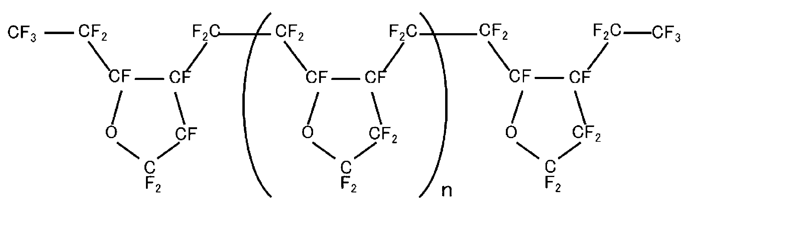
本発光装置1では、このような非結合性の非晶質フッ素樹脂が、基板11の側面に形成した凹部50の内部に入り込む。これにより、上述のように、アンカー効果によって基板11の側面と封止樹脂40との密着性及び結合力が向上することで、剥離が防止される。そして、基板11の側面と封止樹脂40との密着性及び結合力が高められて剥離が防止されることで、併せて基板11の裏面112と封止樹脂40との剥離も防止される。
以上の通り、本発光装置1では、非結合性の非晶質フッ素樹脂を封止樹脂40として使用することで、光化学反応に起因する電気的特性の劣化及び非晶質フッ素樹脂の分解等を防止することができる。そして、基板11の側面に形成した凹部50の内部に封止樹脂40が入り込むことで得られるアンカー効果によって、非結合性の非晶質フッ素樹脂を使用する場合に問題となる、基板11の裏面112及び側面からの非晶質フッ素樹脂の剥離を防止することができるため、紫外線の素子外部への取り出し効率の低下を防止することができる。
[基板側面に形成される凹部の一例]
次に、本発光装置1における基板11の側面に形成される凹部について、図面を参照して説明する。図6は、基板11の側面を模式的に示す平面図である。図7は、図6に示した基板11の側面の一部(粗面帯51a,51b付近)を示す写真である。尚、図6及び図7の上下方向は、図3及び図4の上下方向と同じである。
次に、本発光装置1における基板11の側面に形成される凹部について、図面を参照して説明する。図6は、基板11の側面を模式的に示す平面図である。図7は、図6に示した基板11の側面の一部(粗面帯51a,51b付近)を示す写真である。尚、図6及び図7の上下方向は、図3及び図4の上下方向と同じである。
図6(A)及び(B)は、異なる2種類の凹部50a,50bを示したものである。図6(A)は、基板11の側面に形成された複数の凹部50aが断続的に連なって粗面帯51aを形成(換言すると、隣接する凹部50aが離間した状態で一列に並ぶことで粗面帯51aを形成)しており、基板11の側面に4本の粗面帯51aが形成されている場合を例示している。また、図6(B)は、基板11の側面に形成された複数の凹部50bが連続的に連なって粗面帯51bを形成(換言すると、隣接する凹部50bの端部が結合した状態で一列に並ぶことで粗面帯51bを形成)しており、基板11の側面に4本の粗面帯51bが形成されている場合を例示している。尚、図6(A)及び(B)に例示する粗面帯51a,51bは、隣接する凹部50a,50bの間隔が異なるだけであるとも言い得る。
図7(A)及び(B)に示す粗面帯51c,51dは、図6(A)の粗面帯51aと同様に、凹部50c,50dが断続的に連なってなるものである。但し、図7(B)の凹部50dは、図7(A)の凹部50cよりも細く、図7(A)の凹部50cよりも隣接する間隔が狭くなっている。また、図7(C)に示す粗面帯51eは、図6(B)の粗面帯51bと同様に、凹部50eが連続的に連なってなるものである。
図6及び図7に示したような凹部50a~50eは、ウェハを切断して本発光素子10(チップ)を得るダイシング工程によって基板11の側面が表出した後に、基板11の側面に対してブラスト処理(例えば、ダイヤモンド等のサファイアと同等以上の硬さの粒子を吹き付ける処理)等を行うことで形成することも可能である。しかし、当該凹部50a~50eを、ダイシング工程と同時に形成することができれば、工数の増加を防止することができるため、好ましい。そこで、以下の[本発光装置の製造方法]では、ダイシング工程と同時に基板11の側面に対して凹部50a~50eを形成する方法について説明する。
[本発光装置の製造方法]
本発光装置10の製造方法について、図面を参照して説明する。先ず、ウェハ状態(チップに切断される前の状態)であるサファイア基板11の主面111上に、周知の窒化物半導体の製造工程により、半導体積層部12、n電極13、p電極14、及び、保護膜等を形成する。これにより、図8に示すようなウェハ60が得られる。尚、図8はダイシング工程前のウェハ60の形状を模式的に示す平面図であり、ウェハ60をp電極14及びn電極13側から見た場合の平面図である。
本発光装置10の製造方法について、図面を参照して説明する。先ず、ウェハ状態(チップに切断される前の状態)であるサファイア基板11の主面111上に、周知の窒化物半導体の製造工程により、半導体積層部12、n電極13、p電極14、及び、保護膜等を形成する。これにより、図8に示すようなウェハ60が得られる。尚、図8はダイシング工程前のウェハ60の形状を模式的に示す平面図であり、ウェハ60をp電極14及びn電極13側から見た場合の平面図である。
図8に示すように、ウェハ60は、ウェハ60の切断後にチップ(本発光素子10)となるチップ領域61がマトリクス状に配置されている。このウェハ60において、チップ領域61の境界となる面が、ダイシング工程によって切断すべき面である切断予定面62である。尚、図8に示すウェハ60において、チップ領域61の境界(切断予定面62)の近傍の最表面は、n電極13を形成するために露出させたn型クラッド層22であるが、当該n型クラッド層22をさらに除去して基板11を露出させても良い。
本製造方法では、ダイシング工程においてステルスダイシングを行う。ステルスダイシングとは、基板11を透過する波長のレーザ光を基板11の内部で集光させることで切断予定面61に損傷を与えた上で、ウェハ60を切断するという手法である。
ステルスダイシングの工程の一例を、図9~図11に示す。図9~図11は、本製造方法の一例を模式的に示す工程断面図である。本製造方法では、図9(A)、図9(B)及び図10、図9(C)、図11(A)、図11(B)、図11(C)の順番で夫々の工程を行う。尚、図10は、図9(B)と同じ工程を示した工程断面図であり、図9(B)に対して垂直な断面を示している。また、図9~図11の上下方向も、図3及び図4の上下方向と同じである。
最初に、図9(A)に示すように、ウェハ60における基板11の主面111側(以下、単に「主面側」と称する)を、第1シート70に対して貼り付ける。
次に、図9(B)に示すように、ウェハ60における基板11の裏面112側(以下、単に「裏面側」と称する)にレーザ光71を照射する。このとき、集光レンズ72を用いて、基板11の裏面112から内部に入射するレーザ光71を切断予定面62に集光させる。例えば、レーザ光71は、サファイア基板11を透過する波長(具体的に例えば、Nd-YAGレーザの第2高調波である532nmや第3高調波である355nmなど)であり、ウェハ60に対してパルスで照射される。基板11の内部でレーザ光71を集光すると、集光領域73において光吸収が生じて局所的に温度が上がることで、当該集光領域73が溶融または膨張するなどして損傷を受ける。そして、図10に示すように、基板11の主面111に対して平行な方向(図中の黒塗りの矢印の方向)に沿って集光領域73の位置を移動させながらレーザ光71を照射することで、帯状の改質層510(ウェハ60の切断後に粗面帯51になる部分)を形成する。更に、基板11の主面111に対して垂直な方向(図中の上下方向)における集光領域73の位置を変更した上で、再度、基板11の主面111に対して平行な方向に沿って集光領域73の位置を移動させながらレーザ光71を照射することで、基板11の切断予定面62に複数の改質層510を形成する。尚、集光領域73の位置は、ウェハ60及び光学系(レーザ光71の光源や集光レンズ72など)の少なくとも一方を駆動することで移動させることができる。
図9(B)及び図10の工程が終了すると、図9(C)に示すように、ウェハ60における切断予定面62(図8参照)の全てに改質層510が形成された状態になる。次に、図11(A)に示すように、ウェハ60の裏面側(基板11の裏面)に第2シート74を貼り付ける。そして、図11(B)に示すように、ウェハ60の主面側の切断予定面62を避けた位置にブロック75を配置するとともに、ウェハ60の裏面側の切断予定面62の直上となる位置にブレード76を押し当てることで、ウェハ60を切断する。このとき、ウェハ60(基板11)の切断予定面62は、ダメージを受けている改質層510が形成されて切断され易くなっているため、切断予定面62に沿ってウェハ60が切断される。そして、このウェハ60の切断によって得られる基板11の側面には、改質層510を切断することで凹部50及び粗面帯51が表出している。尚、基板11の側面に表出する凹部50及び粗面帯51の形状は、図9(B)及び図10の工程において改質層510を形成するために基板11に入射するレーザ光の特性(強度、パルス幅、パルス間隔など)に応じて決まる。例えば、レーザ光の強度及びパルス幅を大きくするほど大きな凹部50が形成され得るし、レーザ光のパルス幅及びパルス間隔を小さくするほど細かく高密度な凹部50が形成され得る。
図11(B)の工程が終了すると、図11(C)に示すように、ウェハ60から全てのチップ(本発光素子10)が切り出された状態になる。この後、例えば第1シート70及び第2シート74から剥離してピックアップした本発光素子10を、サブマウント30の第1及び第2金属電極配線32,33上に、周知のフリップチップ実装により固定する。具体的には、p電極14と第1金属電極配線32が、金バンプ等を介して、物理的且つ電気的に接続し、n電極13と第2金属電極配線33が、金バンプ等を介して、物理的且つ電気的に接続する(図3参照)。
引き続き、非結合性の非晶質フッ素樹脂を、含フッ素溶媒、好ましくは、非プロトン性含フッ素溶媒に溶解した塗工液を、サブマウント30及び本発光素子10上に、剥離性の良いテフロンニードル等を用いて注入した後、塗工液を徐々に加熱しながら溶媒を蒸発させて、本発光素子10の上面と側面(基板11の裏面112及び側面、半導体積層部12の側面、n電極13及びp電極14の側面)、サブマウント30の上面(第1及び第2金属電極配線32,33の上面及び側面、第1及び第2金属電極配線32,33間に露出した基材31の表面)、サブマウント30と本発光素子10の間の間隙部に、非結合性の非晶質フッ素樹脂の封止樹脂40を形成する(図3参照)。このとき、基板11の側面に形成された凹部50の内部に、封止樹脂40が入り込んだ状態になる(図4参照)。尚、この工程における溶媒の蒸発に当たっては、封止樹脂40内に気泡が残らないように、溶媒の沸点以下の低温域(例えば、室温付近)から溶媒の沸点以上の高温域(例えば、200℃付近)まで徐々に加熱して、溶媒を蒸発させる。
引き続き、封止樹脂40の上部に、封止樹脂40と同じ非結合性の非晶質フッ素樹脂製のレンズ41を、例えば射出成形、トランスファー成形、圧縮成形等により、本発光素子10を覆うように形成する(図3参照)。当該各成形用の成形型は、金属型、シリコーン樹脂型、または、これらの組み合わせを使用できる。
以上の通り、本製造方法では、ステルスダイシングを行うことで基板11の側面に生じた凹部50の内部に非晶質フッ素樹脂である封止樹脂40を入り込ませ、アンカー効果によって基板11の側面と封止樹脂40との密着性及び結合力を向上させて剥離を防止した本発光装置1が製造される。従って、基板11の側面に凹部50を形成する工程を別途必要とすることなく、チップの量産に必要なウェハ60のダイシングをステルスダイシングで行うだけで、封止樹脂40の剥離を防止した本発光装置1を製造することができる。
尚、封止樹脂40の形成後に、非結合性の非晶質フッ素樹脂の分解が開始する温度(約350℃)以下の温度範囲、例えば、150℃~300℃、より好ましくは、200℃~300℃の温度範囲で、封止樹脂40を加熱して軟化させ、本発光素子10の側面(または側面及び上面)の封止樹脂40を本発光素子10側に向けて押圧しても良い。これにより、封止樹脂40は圧縮された状態で、凹部50の内部に密に充填される。この結果、凹部50の内部に充填された封止樹脂40がより抜け難くなり、アンカーとして確実に機能する。この封止樹脂40の加熱処理及び押圧処理は、レンズ41の形成と同時に行っても良い。或いは、加熱処理だけを先に行い、押圧処理をレンズ41の形成と同時に行っても良い。また、加熱処理及び押圧処理の一方のみを行っても良い。
[別実施形態]
以下に、上記実施形態の変形例につき説明する。
以下に、上記実施形態の変形例につき説明する。
〈1〉上記実施形態では、本発光素子10をサブマウント30にフリップチップ実装する一態様として、p電極14と第1金属電極配線32、n電極13と第2金属電極配線33を、金バンプを介して接続する場合を説明したが、p電極14とn電極13の各上面が同一平面となるように高さを揃えて形成されている場合等において、リフロー方式等の周知のはんだ付け方法で、p電極14と第1金属電極配線32、n電極13と第2金属電極配線33を、はんだ材料(ボンディング材料)を介して物理的且つ電気的に接続しても良い。尚、p電極14とn電極13の各上面が同一平面となるように高さを揃える方法として、例えば、p電極14と電気的に接続し、絶縁保護膜を介して、上記メサ部分の上面及び側面を覆うようにp側のメッキ電極を形成し、当該p側のメッキ電極から離間して、n電極13と電気的に接続するn側のメッキ電極を、p側のメッキ電極と同じ高さに、電解メッキ法等により形成する方法が考えられる。尚、当該メッキ電極の詳細については、国際出願(PCT/JP2015/060588)の明細書等の記載が参考になる。
〈2〉上記実施形態では、1つの本発光素子10をサブマウント30上に載置した本発光装置1について説明したが、本発光装置1は、サブマウントまたはプリント基板等の基台上に、複数の本発光素子10を載置して構成しても良い。この場合、複数の本発光素子10を封止樹脂40で、まとめて封止しても良く、また、1つずつ個別に封止しても良い。この場合、例えば、基台の表面に、封止する単位の1または複数の本発光素子1の周りを囲む樹脂ダムを形成しておき、その樹脂ダムで囲まれた領域に、例えば、上記実施形態で説明した要領で、封止樹脂40を形成する。尚、本発光素子10を載置する基台は、サブマウント及びプリント基板に限定されるものではない。
また、1つの本発光素子10をサブマウント30上に載置する場合においても、1枚の基材31の表面側に、複数のサブマウント30の第1及び第2金属電極配線32,33を形成し、1枚の基材31の裏面側に、複数のサブマウント30のリード端子34,35を形成し、複数のサブマウント30をマトリクス状に配置したサブマウント板に、複数の本発光素子10を夫々各サブマウント30上にフリップチップ実装し、複数の本発光素子10に対して夫々封止樹脂40または封止樹脂40とレンズ41を形成した後に、当該サブマウント板を個々のサブマウント30に分割して、1つの本発光素子10をサブマウント30上に載置してなる本発光装置1を製造しても良い。
〈3〉上記実施形態では、基板11の側面において、基板11の主面111に対して平行な複数本(4本)の粗面帯51が、基板11の主面111に垂直な方向に対して均一に分散して形成される場合について例示したが(例えば、図6(A)及び(B)参照)、粗面帯51の態様はこの例の限りではない。以下、粗面帯51の変形例について図面を参照して説明する。尚、以下で参照する、凹部50及び粗面帯51の変形例を模式的に示す平面図である図12及び図13は、図6(A)及び(B)に示す平面図と同様の基板11の平面を示したものである。
図12(A)に示す粗面帯51fは、上記実施形態のように基板11の主面111に垂直な方向に対して均一に分散しておらず、基板11の主面111側に偏って分布している。一方、図12(B)に示す粗面帯51gは、基板11の主面111とは反対側(即ち、基板11の裏面112側)に偏って分布している。上述のように、粗面帯51は、ウェハ60の改質層510が形成される位置に形成される。また、基板11の主面111上には半導体積層部12が形成されている(図9~11参照)。
図12(A)に示すように、粗面帯51fが基板11の主面111側に偏って分布している場合、ウェハ60の改質層510が基板11の主面111側に偏って形成されているため、基板11の主面111付近における切断位置の精度を高めて半導体積層部12の割れまたは欠け(チッピング不良)を抑制したステルスダイシングが行われる。一方、図12(B)に示すように、粗面帯51gが基板11の裏面112側に偏って分布する場合、ウェハ60の改質層510が基板11の裏面112側に偏って形成されているため、集光させたレーザ光71の熱が半導体積層部12に影響を与え難いステルスダイシングが行われる。また、図6(A)及び(B)に示したような、粗面帯51a,51bが基板11の主面111に垂直な方向に対して均一に分布している場合、ウェハ60の改質層510が基板11の主面111に垂直な方向に対して均一に分布して形成されているため、当該方向に対するウェハ60の均一な切断が可能なステルスダイシングが行われる。
尚、図12(B)に示すように、基板11の裏面112側に粗面帯51gが偏って分布していると、基板11の裏面112付近において強力なアンカー効果を発揮させることができる。そのため、フリップチップ実装した本発光素子10における光(紫外線)の主たる出射面である基板11の裏面112における封止樹脂40の剥離を効果的に防止することができる。
また、図13(A)~(C)に示す粗面帯51h~51jは、基板11の主面111に対して平行になっていない。特に、図13(A)に示す粗面帯51hは全て平行であるが、図13(B)に示す粗面帯51iは一部が平行ではなく、図13(C)に示す粗面帯51jは屈曲している。ただし、粗面帯51h~51jは、いずれも基板11の主面111に対して平行な成分を有する方向に延伸したものである。そのため、このような粗面帯51h~51jが形成される場合であっても、基板11の主面111に対して平行な成分を有する方向に延伸する改質層510がウェハ60に形成されるため、ウェハ60を基板11の主面111に平行な方向に沿って容易に切断することができる。
〈4〉上記実施形態において、ウェハ60に対して形成すべき改質層510を1本としても、ステルスダイシングを行うことは可能であり、基板11の側面と封止樹脂40との密着性及び結合力を向上させる効果を得ることも可能である。ただし、本発光装置1では、光(紫外線)の取り出し効率を向上させるために、基板11の厚さを大きくする(例えば、400μm程度)ことがある(例えば、国際公開第2015/111134号参照)。この場合、基板11の厚さに対して改質層510の数が不足すれば、切断予定面62に沿って切断することが困難になり得る。
この点、基板11の厚さをXμmとしたとき、改質層510の本数(粗面帯51の本数)をX/200本以上にすれば、ある程度確実に切断予定面62に沿ってウェハ60をステルスダイシングによって切断することが可能である。更に、改質層510の本数(粗面帯51の本数)をX/150本以上にすれば、チッピング不良などの不良の発生率が1%よりも低くなる極めて良好なステルスダイシングを行うことが可能になる。
〈5〉上記実施形態では、本発光素子10における基板11の側面において、凹部50が連なってなる粗面帯51が形成される場合について例示しているが、基板11の側面に凹部50が形成されていれば、必ずしも粗面帯51が形成されていなくてもよい。この場合の一例を、図面を参照して説明する。図14は、基板11の側面に形成される凹部の変形例を模式的に示す平面図である。なお、図14は、図6(A)及び(B)に示す平面図と同様の基板11の平面を示したものである。
図14(A)に示す凹部50kは、基板11の側面に対してランダムに分散して形成されたものである。このような凹部50kは、例えば、ステルスダイシングを行う際におけるレーザ光71の集光領域73の位置をランダムに移動させることでも形成可能であるが(図9(B)及び図10参照)、ウェハ60を周知または新規のダイシング技術によって切断した後に、基板11の側面に対してブラスト処理等を行うことでも形成可能である。また、図14(B)に示す凹部50lは、基板11の側面に対して規則的に分散して形成されたものである。このような凹部50lは、例えば、ステルスダイシングを行う際におけるレーザ光71の集光領域73の位置を規則的に移動させることで形成可能である。
このような凹部50k,50lが形成される場合であっても、アンカー効果によって基板11の側面と封止樹脂40との密着性及び結合力を向上させて剥離を防止することが可能であるとともに、ステルスダイシングも可能である。
〈6〉上記実施形態では、封止樹脂40の上部に、封止樹脂40と同じ非結合性の非晶質フッ素樹脂製のレンズ41を形成したが、レンズ41を形成せずに、他の樹脂部分の形成等を行っても良い。例えば、フリップチップ実装で使用する基台が、図5に例示したようなサブマウント30ではなく、基材31の外周部分に、フリップチップ実装後の本発光素子10の上面より高い、本発光素子10を取り囲む側壁が設けられている場合、封止樹脂40上の当該側壁に囲まれた空間内に、固体状の非結合性の非晶質フッ素樹脂を入れて、例えば、250℃~300℃の高温で溶融させ、その後徐々に冷却して第2の封止樹脂層を形成しても良い。また、必要に応じて、当該第2の封止樹脂膜上に、レンズ41を形成しても良い。
本発明に係る窒化物半導体紫外線発光装置は、発光中心波長が約350nm以下の裏面出射型の発光ダイオードに利用可能である。
1: 窒化物半導体紫外線発光装置
10: 窒化物半導体紫外線発光素子
11: サファイア基板
111: 主面
112: 裏面
12: 半導体積層部(AlGaN系半導体層)
13: n電極
14: p電極
20: AlN層
21: AlGaN層
22: n型クラッド層
23: 活性層
24: 電子ブロック層
25: p型クラッド層
26: pコンタクト層
30: サブマウント(基台)
31: 基材
32: 第1金属電極配線
320: 第1電極パッド
321: 第1配線部
33: 第2金属電極配線
330: 第2電極パッド
331: 第2配線部
34,35:リード端子
40: 封止樹脂(非晶質フッ素樹脂)
41: レンズ
50,50a~50l:凹部
51,51a~51j:粗面帯
510: 改質層
60: ウェハ
61: チップ領域
62: 切断予定面
70: 第1シート
71: レーザ光
72: 集光レンズ
73: 集光領域
74: 第2シート
75: ブロック
76: ブレード
10: 窒化物半導体紫外線発光素子
11: サファイア基板
111: 主面
112: 裏面
12: 半導体積層部(AlGaN系半導体層)
13: n電極
14: p電極
20: AlN層
21: AlGaN層
22: n型クラッド層
23: 活性層
24: 電子ブロック層
25: p型クラッド層
26: pコンタクト層
30: サブマウント(基台)
31: 基材
32: 第1金属電極配線
320: 第1電極パッド
321: 第1配線部
33: 第2金属電極配線
330: 第2電極パッド
331: 第2配線部
34,35:リード端子
40: 封止樹脂(非晶質フッ素樹脂)
41: レンズ
50,50a~50l:凹部
51,51a~51j:粗面帯
510: 改質層
60: ウェハ
61: チップ領域
62: 切断予定面
70: 第1シート
71: レーザ光
72: 集光レンズ
73: 集光領域
74: 第2シート
75: ブロック
76: ブレード
Claims (10)
- 基台と、
前記基台上にフリップチップ実装された窒化物半導体紫外線発光素子と、
前記窒化物半導体紫外線発光素子に直接接触して被覆する非晶質フッ素樹脂と、を備えてなる紫外線発光装置であって、
前記窒化物半導体紫外線発光素子が、サファイア基板と、前記サファイア基板の主面上に積層された複数のAlGaN系半導体層と、1または複数の金属層からなるn電極と、1または複数の金属層からなるp電極を備えてなり、
前記非晶質フッ素樹脂の末端官能基がパーフルオロアルキル基であり、
前記サファイア基板の側面に形成された凹部の内部に、前記非晶質フッ素樹脂が入り込んでいることを特徴とする窒化物半導体紫外線発光装置。 - 前記サファイア基板の側面に、前記凹部が断続的または連続的に連なってなる粗面帯が形成されていることを特徴とする請求項1に記載の窒化物半導体紫外線発光装置。
- 前記サファイア基板の側面に形成された前記粗面帯が、前記サファイア基板の主面に平行な成分を有する方向に沿って延伸していることを特徴とする請求項2に記載の窒化物半導体紫外線発光装置。
- 前記サファイア基板の側面に、複数本の前記粗面帯が形成されていることを特徴とする請求項3に記載の窒化物半導体紫外線発光装置。
- 前記サファイア基板の側面に形成された前記粗面帯が、前記サファイア基板の主面側に偏って分布していることを特徴とする請求項4に記載の窒化物半導体紫外線発光装置。
- 前記サファイア基板の側面に形成された前記粗面帯が、前記サファイア基板の主面の反対側に偏って分布していることを特徴とする請求項4に記載の窒化物半導体紫外線発光装置。
- 前記サファイア基板の側面に形成された前記粗面帯が、前記サファイア基板の主面に垂直な方向に対して均一に分布していることを特徴とする請求項4に記載の窒化物半導体紫外線発光装置。
- 前記サファイア基板の厚さをXμmとしたとき、前記サファイア基板の側面に形成される前記粗面帯の本数がX/200本以上であることを特徴とする請求項3~7のいずれか1項に記載の窒化物半導体紫外線発光装置。
- 前記サファイア基板の厚さをXμmとしたとき、前記サファイア基板の側面に形成される前記粗面帯の本数がX/150本以上であることを特徴とする請求項3~7のいずれか1項に記載の窒化物半導体紫外線発光装置。
- 請求項1~9のいずれか1項に記載の窒化物半導体紫外線発光装置の製造方法であって、
前記サファイア基板を透過する波長のレーザ光を前記サファイア基板の主面の反対側から入射させ、前記サファイア基板の内部で集光することで、前記サファイア基板の内部の切断予定面に損傷を与える第1工程と、
前記切断予定面で前記サファイア基板を切断することで、前記凹部が表出した前記サファイア基板の側面を得る第2工程と、
前記非晶質フッ素樹脂を所定の溶媒に溶解してなる塗工液を、前記窒化物半導体紫外線発光素子と前記基台の各露出表面を被覆し、前記窒化物半導体紫外線発光素子と前記基台の間隙部を充填するように塗布する第3工程と、
前記溶媒を蒸発させて、前記窒化物半導体紫外線発光素子と前記基台の各露出表面を被覆し、前記窒化物半導体紫外線発光素子と前記基台の間隙部を充填するとともに、前記サファイア基板の側面に形成された前記凹部の内部に入り込む前記非晶質フッ素樹脂の層を形成する第4工程と、
を有することを特徴とする窒化物半導体紫外線発光装置の製造方法。
Priority Applications (3)
| Application Number | Priority Date | Filing Date | Title |
|---|---|---|---|
| US16/301,373 US20200321491A1 (en) | 2016-06-03 | 2017-02-27 | Nitride semiconductor ultraviolet light emitting device and method for manufacturing same |
| CN201780033986.4A CN109314166A (zh) | 2016-06-03 | 2017-02-27 | 氮化物半导体紫外线发光装置及其制造方法 |
| JP2018520369A JPWO2017208535A1 (ja) | 2016-06-03 | 2017-02-27 | 窒化物半導体紫外線発光装置及びその製造方法 |
Applications Claiming Priority (2)
| Application Number | Priority Date | Filing Date | Title |
|---|---|---|---|
| JP2016-112084 | 2016-06-03 | ||
| JP2016112084 | 2016-06-03 |
Publications (1)
| Publication Number | Publication Date |
|---|---|
| WO2017208535A1 true WO2017208535A1 (ja) | 2017-12-07 |
Family
ID=60479294
Family Applications (1)
| Application Number | Title | Priority Date | Filing Date |
|---|---|---|---|
| PCT/JP2017/007342 Ceased WO2017208535A1 (ja) | 2016-06-03 | 2017-02-27 | 窒化物半導体紫外線発光装置及びその製造方法 |
Country Status (5)
| Country | Link |
|---|---|
| US (1) | US20200321491A1 (ja) |
| JP (1) | JPWO2017208535A1 (ja) |
| CN (1) | CN109314166A (ja) |
| TW (1) | TW201806197A (ja) |
| WO (1) | WO2017208535A1 (ja) |
Cited By (4)
| Publication number | Priority date | Publication date | Assignee | Title |
|---|---|---|---|---|
| CN110350070A (zh) * | 2018-04-06 | 2019-10-18 | 旭化成株式会社 | 紫外线发光元件、紫外线发光装置、半导体芯片和透镜的接合方法 |
| JP2020025089A (ja) * | 2018-07-27 | 2020-02-13 | 住友化学株式会社 | Ledデバイス、ledデバイスの製造方法および積層体 |
| CN112420644A (zh) * | 2019-08-20 | 2021-02-26 | 三星电子株式会社 | 包括低k介电层的半导体芯片 |
| US12408493B2 (en) | 2021-05-26 | 2025-09-02 | Nichia Corporation | Light-emitting element including first semiconductor layer having exposed portion with first region and second regions |
Families Citing this family (6)
| Publication number | Priority date | Publication date | Assignee | Title |
|---|---|---|---|---|
| US11217726B2 (en) * | 2018-02-14 | 2022-01-04 | Soko Kagaku Co., Ltd. | Nitride semiconductor ultraviolet light-emitting element |
| TWI706537B (zh) | 2019-05-28 | 2020-10-01 | 友達光電股份有限公司 | 自發光元件及發光裝置的製造方法 |
| CN112086547A (zh) | 2019-06-13 | 2020-12-15 | 光宝光电(常州)有限公司 | 发光二极管封装结构 |
| JP7222827B2 (ja) * | 2019-06-21 | 2023-02-15 | スタンレー電気株式会社 | 半導体装置、および、その製造方法 |
| CN111403580A (zh) * | 2020-03-24 | 2020-07-10 | 营口众恩光电科技有限公司 | 一种紫外led封装结构及封装方法 |
| WO2022252137A1 (zh) * | 2021-06-02 | 2022-12-08 | 泉州三安半导体科技有限公司 | 发光二极管及其制作方法 |
Citations (5)
| Publication number | Priority date | Publication date | Assignee | Title |
|---|---|---|---|---|
| JP2003249682A (ja) * | 2002-02-22 | 2003-09-05 | Toshiba Corp | 半導体発光装置 |
| JP2008098465A (ja) * | 2006-10-13 | 2008-04-24 | Aisin Seiki Co Ltd | 半導体発光素子の分離方法 |
| JP2012016726A (ja) * | 2010-07-08 | 2012-01-26 | Mitsubishi Chemicals Corp | 窒化物材料の加工方法、半導体機能素子の製造方法、半導体発光素子の製造方法、半導体発光素子アレイ、半導体発光素子およびレーザ加工装置 |
| US20130248500A1 (en) * | 2010-11-29 | 2013-09-26 | Yuri Georgievich Shreter | Method of Separating Surface Layer of Semiconductor Crystal Using a Laser Beam Perpendicular to the Separating Plane |
| WO2014178288A1 (ja) * | 2013-04-30 | 2014-11-06 | 創光科学株式会社 | 紫外線発光装置 |
Family Cites Families (3)
| Publication number | Priority date | Publication date | Assignee | Title |
|---|---|---|---|---|
| JP4385746B2 (ja) * | 2003-11-28 | 2009-12-16 | 三菱化学株式会社 | 窒化物系半導体素子の製造方法 |
| JP2006245062A (ja) * | 2005-02-28 | 2006-09-14 | Toyoda Gosei Co Ltd | Iii族窒化物系化合物半導体素子の製造方法及び発光素子 |
| JP5221007B2 (ja) * | 2006-05-31 | 2013-06-26 | アイシン精機株式会社 | 発光ダイオードチップ及びウェハ分割加工方法 |
-
2017
- 2017-02-27 JP JP2018520369A patent/JPWO2017208535A1/ja active Pending
- 2017-02-27 US US16/301,373 patent/US20200321491A1/en not_active Abandoned
- 2017-02-27 WO PCT/JP2017/007342 patent/WO2017208535A1/ja not_active Ceased
- 2017-02-27 CN CN201780033986.4A patent/CN109314166A/zh active Pending
- 2017-03-07 TW TW106107414A patent/TW201806197A/zh unknown
Patent Citations (5)
| Publication number | Priority date | Publication date | Assignee | Title |
|---|---|---|---|---|
| JP2003249682A (ja) * | 2002-02-22 | 2003-09-05 | Toshiba Corp | 半導体発光装置 |
| JP2008098465A (ja) * | 2006-10-13 | 2008-04-24 | Aisin Seiki Co Ltd | 半導体発光素子の分離方法 |
| JP2012016726A (ja) * | 2010-07-08 | 2012-01-26 | Mitsubishi Chemicals Corp | 窒化物材料の加工方法、半導体機能素子の製造方法、半導体発光素子の製造方法、半導体発光素子アレイ、半導体発光素子およびレーザ加工装置 |
| US20130248500A1 (en) * | 2010-11-29 | 2013-09-26 | Yuri Georgievich Shreter | Method of Separating Surface Layer of Semiconductor Crystal Using a Laser Beam Perpendicular to the Separating Plane |
| WO2014178288A1 (ja) * | 2013-04-30 | 2014-11-06 | 創光科学株式会社 | 紫外線発光装置 |
Cited By (5)
| Publication number | Priority date | Publication date | Assignee | Title |
|---|---|---|---|---|
| CN110350070A (zh) * | 2018-04-06 | 2019-10-18 | 旭化成株式会社 | 紫外线发光元件、紫外线发光装置、半导体芯片和透镜的接合方法 |
| JP2020025089A (ja) * | 2018-07-27 | 2020-02-13 | 住友化学株式会社 | Ledデバイス、ledデバイスの製造方法および積層体 |
| CN112420644A (zh) * | 2019-08-20 | 2021-02-26 | 三星电子株式会社 | 包括低k介电层的半导体芯片 |
| US12604727B2 (en) | 2019-08-20 | 2026-04-14 | Samsung Electronics Co., Ltd. | Semiconductor chip including low-k dielectric layer |
| US12408493B2 (en) | 2021-05-26 | 2025-09-02 | Nichia Corporation | Light-emitting element including first semiconductor layer having exposed portion with first region and second regions |
Also Published As
| Publication number | Publication date |
|---|---|
| US20200321491A1 (en) | 2020-10-08 |
| CN109314166A (zh) | 2019-02-05 |
| TW201806197A (zh) | 2018-02-16 |
| JPWO2017208535A1 (ja) | 2019-03-28 |
Similar Documents
| Publication | Publication Date | Title |
|---|---|---|
| TWI652838B (zh) | Nitride semiconductor ultraviolet light emitting device and method of manufacturing same | |
| CN107408604B (zh) | 氮化物半导体紫外线发光元件以及氮化物半导体紫外线发光装置 | |
| JP6440846B2 (ja) | 窒化物半導体ウェハ及びその製造方法、並びに、窒化物半導体紫外線発光素子及び装置 | |
| US20200321491A1 (en) | Nitride semiconductor ultraviolet light emitting device and method for manufacturing same | |
| JP5313256B2 (ja) | 基板リフトオフに関する強固なled構造 | |
| TWI699011B (zh) | 半導體發光裝置 | |
| WO2018003228A1 (ja) | 紫外線発光装置及びその製造方法 | |
| JP5982179B2 (ja) | 半導体発光装置およびその製造方法 | |
| US9029892B2 (en) | Device module | |
| CN107851693B (zh) | 氮化物半导体发光元件用的基台及其制造方法 | |
| US10109776B2 (en) | Light emitting device having curved light emitting element | |
| KR102279520B1 (ko) | 발광 소자 및 그 제조 방법 |
Legal Events
| Date | Code | Title | Description |
|---|---|---|---|
| ENP | Entry into the national phase |
Ref document number: 2018520369 Country of ref document: JP Kind code of ref document: A |
|
| NENP | Non-entry into the national phase |
Ref country code: DE |
|
| 121 | Ep: the epo has been informed by wipo that ep was designated in this application |
Ref document number: 17806097 Country of ref document: EP Kind code of ref document: A1 |
|
| 122 | Ep: pct application non-entry in european phase |
Ref document number: 17806097 Country of ref document: EP Kind code of ref document: A1 |