WO2017195711A1 - 半導体基板加工用粘着テープ - Google Patents
半導体基板加工用粘着テープ Download PDFInfo
- Publication number
- WO2017195711A1 WO2017195711A1 PCT/JP2017/017293 JP2017017293W WO2017195711A1 WO 2017195711 A1 WO2017195711 A1 WO 2017195711A1 JP 2017017293 W JP2017017293 W JP 2017017293W WO 2017195711 A1 WO2017195711 A1 WO 2017195711A1
- Authority
- WO
- WIPO (PCT)
- Prior art keywords
- layer
- adhesive tape
- semiconductor substrate
- resin
- semiconductor
- Prior art date
- Legal status (The legal status is an assumption and is not a legal conclusion. Google has not performed a legal analysis and makes no representation as to the accuracy of the status listed.)
- Ceased
Links
Images


Classifications
-
- C—CHEMISTRY; METALLURGY
- C09—DYES; PAINTS; POLISHES; NATURAL RESINS; ADHESIVES; COMPOSITIONS NOT OTHERWISE PROVIDED FOR; APPLICATIONS OF MATERIALS NOT OTHERWISE PROVIDED FOR
- C09J—ADHESIVES; NON-MECHANICAL ASPECTS OF ADHESIVE PROCESSES IN GENERAL; ADHESIVE PROCESSES NOT PROVIDED FOR ELSEWHERE; USE OF MATERIALS AS ADHESIVES
- C09J4/00—Adhesives based on organic non-macromolecular compounds having at least one polymerisable carbon-to-carbon unsaturated bond ; adhesives, based on monomers of macromolecular compounds of groups C09J183/00 - C09J183/16
-
- C—CHEMISTRY; METALLURGY
- C09—DYES; PAINTS; POLISHES; NATURAL RESINS; ADHESIVES; COMPOSITIONS NOT OTHERWISE PROVIDED FOR; APPLICATIONS OF MATERIALS NOT OTHERWISE PROVIDED FOR
- C09J—ADHESIVES; NON-MECHANICAL ASPECTS OF ADHESIVE PROCESSES IN GENERAL; ADHESIVE PROCESSES NOT PROVIDED FOR ELSEWHERE; USE OF MATERIALS AS ADHESIVES
- C09J133/00—Adhesives based on homopolymers or copolymers of compounds having one or more unsaturated aliphatic radicals, each having only one carbon-to-carbon double bond, and at least one being terminated by only one carboxyl radical, or of salts, anhydrides, esters, amides, imides, or nitriles thereof; Adhesives based on derivatives of such polymers
-
- C—CHEMISTRY; METALLURGY
- C09—DYES; PAINTS; POLISHES; NATURAL RESINS; ADHESIVES; COMPOSITIONS NOT OTHERWISE PROVIDED FOR; APPLICATIONS OF MATERIALS NOT OTHERWISE PROVIDED FOR
- C09J—ADHESIVES; NON-MECHANICAL ASPECTS OF ADHESIVE PROCESSES IN GENERAL; ADHESIVE PROCESSES NOT PROVIDED FOR ELSEWHERE; USE OF MATERIALS AS ADHESIVES
- C09J7/00—Adhesives in the form of films or foils
- C09J7/20—Adhesives in the form of films or foils characterised by their carriers
Definitions
- the present invention relates to an adhesive tape for processing a semiconductor substrate.
- Examples of the semiconductor device include a module in which a semiconductor element is mounted on a substrate.
- a method for manufacturing the semiconductor device for example, the following method has been proposed.
- a plurality of semiconductor elements are placed on a substrate, and then sealed with a sealing material so as to cover the semiconductor elements placed on the substrate. Get.
- a semiconductor substrate processing adhesive tape is affixed to the substrate side of the semiconductor sealing connector, and the semiconductor sealing connector is placed on the dicer table via the semiconductor substrate processing adhesive tape. Further, the semiconductor sealing connector is diced in the thickness direction corresponding to the semiconductor element included in the semiconductor sealing connector using a dicing blade while the periphery of the semiconductor sealing connector is fixed by wafer ring. As a result, the semiconductor sealed connector is cut and separated (divided into pieces), and the semiconductor sealed body is formed on the semiconductor substrate processing adhesive tape. Thereby, a some semiconductor sealing body is manufactured collectively on the adhesive tape for semiconductor substrate processing.
- the separated semiconductor encapsulant is picked up. Thereafter, bumps electrically connected to electrodes provided in the semiconductor element are formed on the lower surface side of the substrate through conductor posts formed in advance on the substrate included in the semiconductor sealing body, thereby obtaining a semiconductor device.
- the semiconductor substrate processing adhesive tape generally has a base material (film base material) and an adhesive layer formed on the base material, and the semiconductor sealed connector is fixed by the adhesive layer.
- the adhesive layer usually contains an adhesive base resin, a photocurable resin, and the like so that the semiconductor sealing body formed after the dicing process of the semiconductor sealing connector can be easily picked up. It is comprised with the resin composition. When energy is applied to such an adhesive layer after the dicing step, the resin composition is cured and the adhesiveness of the adhesive layer is lowered. That is, the pressure-sensitive adhesive layer is designed to facilitate picking up the semiconductor sealing body after the dicing process.
- the semiconductor substrate processing adhesive is caused by friction between the dicing blade and the semiconductor sealing connector.
- the tape is heated. Therefore, when the base material of the adhesive tape for processing a semiconductor substrate is configured to include a cut layer and an extended layer laminated on the side opposite to the adhesive layer of the cut layer, the extended layer that contacts the dicer table
- the base material of the adhesive tape for processing a semiconductor substrate is configured to include a cut layer and an extended layer laminated on the side opposite to the adhesive layer of the cut layer, the extended layer that contacts the dicer table
- it softens and melts by this heating and is fused to the dicer table, resulting in adverse effects on workability and throughput.
- the expansion layer is made of a material having a high melting point.
- the difference in melting point between the adhesive layer and the expansion layer is increased, and the adhesive tape for processing a semiconductor substrate is warped.
- An object of the present invention is to provide a pressure-sensitive adhesive tape for processing a semiconductor substrate capable of suppressing or preventing fusion of an extension layer to a dicer table while accurately preventing warpage in a dicing process.
- a pressure-sensitive adhesive tape for processing a semiconductor substrate comprising a base material and an adhesive layer laminated on one surface of the base material,
- the base material has a notch layer located on the one surface side, and an extension layer laminated on the other surface of the notch layer
- the adhesive tape for processing a semiconductor substrate, wherein the expansion layer has a tack force of 1 kPa to 200 kPa at 80 ° C.
- the pressure-sensitive adhesive tape for processing a semiconductor substrate includes a step of temporarily fixing the semiconductor substrate to the base material via the pressure-sensitive adhesive layer, and cutting the semiconductor substrate in a thickness direction into pieces to process the pressure-sensitive adhesive layer. 10.
- the breaking elongation of the base material measured according to JIS K 6734 is 50% or more and 400% or less.
- the tack force of the expansion layer is 1 kPa or more and 200 kPa or less at 80 ° C.
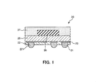
- FIG. 1 is a longitudinal sectional view showing an example of a semiconductor device manufactured using the adhesive tape for processing a semiconductor substrate of the present invention.
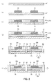
- FIG. 2 is a longitudinal sectional view for explaining a method of manufacturing the semiconductor device shown in FIG. 1 using the adhesive tape for processing a semiconductor substrate of the present invention.
- FIG. 3 is a longitudinal sectional view for explaining a method of manufacturing the semiconductor device shown in FIG. 1 using the adhesive tape for processing a semiconductor substrate of the present invention.
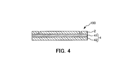
- FIG. 4 is a longitudinal sectional view showing an embodiment of the adhesive tape for processing a semiconductor substrate of the present invention.
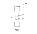
- FIG. 5 is a plan view showing a test piece used when measuring the elongation at break of the base material provided in the adhesive tape for processing a semiconductor substrate of the present invention.
- FIG. 6 is a longitudinal sectional view for explaining a method of manufacturing the adhesive tape for processing a semiconductor substrate shown in FIG.
- the adhesive tape for processing a semiconductor substrate of the present invention will be described in detail. First, prior to describing the adhesive tape for processing a semiconductor substrate of the present invention, a semiconductor device manufactured using the adhesive tape for processing a semiconductor substrate of the present invention will be described.
- FIG. 1 is a longitudinal sectional view showing an example of a semiconductor device manufactured using the adhesive tape for processing a semiconductor substrate of the present invention.
- the upper side in FIG. 1 is referred to as “upper” and the lower side is referred to as “lower”.
- a semiconductor device 20 shown in FIG. 1 includes an interposer (substrate) 25 provided with a conductor post (not shown) disposed so as to penetrate in the thickness direction, a semiconductor element 26 disposed on the interposer 25, and a semiconductor.
- the interposer 25 is a substrate that supports the semiconductor element 26, and its planar view shape is usually a square such as a square or a rectangle.
- the interposer 25 is formed with a plurality of through holes (not shown) penetrating in the thickness direction, and conductor posts are provided corresponding to the through holes.
- An electrode pad is provided on the lower surface side of the semiconductor element 26.
- a semiconductor element 26 (one in this embodiment) is arranged on the interposer 25 so that the electrode pads correspond to the conductor posts.
- the sealing portion 27 is formed so as to cover the upper surface side of the semiconductor element 26 and the interposer 25.
- the conductor post formed corresponding to the through hole of the interposer 25 is electrically connected to the electrode pad provided in the semiconductor element 26 at the upper end thereof.
- a wiring 23 formed in a predetermined shape is provided on the lower surface of the interposer 25. A part of the wiring 23 is electrically connected to the lower end of the conductor post.
- the bumps 21 forming a spherical body are electrically connected to the lower surface of the wiring 23.
- the semiconductor element 26 and the bump 21 are electrically connected via the electrode pad, the conductor post, and the wiring 23.
- a covering portion 22 having an opening 221 for exposing the bump 21 from below is provided so as to cover the wiring 23.
- the semiconductor device 20 includes one semiconductor element 26, but the configuration is not limited thereto.
- the semiconductor device may include two or more semiconductor elements 26, or may further include an electronic component different from the semiconductor elements 26.
- the semiconductor device having such a configuration is manufactured, for example, as follows using the adhesive tape for processing a semiconductor substrate of the present invention.
- FIG. 2 and 3 are longitudinal sectional views for explaining a method of manufacturing the semiconductor device shown in FIG. 1 using the adhesive tape for processing a semiconductor substrate of the present invention.
- the upper side in FIG. 2 is referred to as “upper” and the lower side is referred to as “lower”.
- a flat sheet material 25 ′ as shown in FIG. 2A is prepared, and a plurality of semiconductor elements 26 are arranged (placed) on the sheet material 25 ′ (FIG. 2).
- the sheet material 25 ′ includes a plurality of through holes (not shown) formed in advance, and further includes a conductor post (not shown) embedded corresponding to the through holes.
- the conductor posts are formed at positions corresponding to electrode pads (terminals) included in the semiconductor element 26 when the semiconductor element 26 is disposed on the sheet material 25 ′. That is, in the sheet material 25 ′, the number of conductor posts provided corresponding to the through holes and the total number of electrode pads included in the plurality of semiconductor elements 26 disposed on the sheet material 25 ′ are the same. Is formed.
- the sheet material 25 ′ is cut into pieces in the thickness direction to be separated into individual pieces, thereby forming an interposer 25 (substrate) included in the semiconductor device 20 and exhibiting a function of supporting the semiconductor element 26.
- the sheet material 25 ′ is not particularly limited as long as it has a hardness that can support the semiconductor element 26.
- the sheet material 25 ′ is either a rigid substrate (hard substrate) or a flexible substrate (flexible substrate) such as a core substrate composed of a core material, a build-up substrate composed of a build-up material, Also good.
- a buildup substrate is particularly preferable.
- a build-up substrate is preferably used because it is particularly excellent in processability.
- the build-up material is not particularly limited, but for example, curing a resin composition containing a thermosetting resin such as a phenol resin, a urea resin, a melamine resin, and an epoxy resin, a curing agent, and an inorganic filler.
- a thermosetting resin such as a phenol resin, a urea resin, a melamine resin, and an epoxy resin, a curing agent, and an inorganic filler.
- the core substrate is not particularly limited, and examples thereof include those mainly composed of a thermosetting resin such as cyanate resin, epoxy resin, and bismaleimide-triazine resin.
- the flexible substrate is not particularly limited.
- polyimide polyethylene terephthalate (PET), polyethylene naphthalate (PEN), polyethersulfone (PES), polytetrafluoroethylene (PTFE), polyimide benzoxazole (PIBO).
- PET polyethylene terephthalate
- PEN polyethylene naphthalate
- PES polyethersulfone
- PTFE polytetrafluoroethylene
- PIBO polyimide benzoxazole
- thermoplastic resin such as a liquid crystal polymer.
- the semiconductor element 26 when the semiconductor element 26 is disposed on the sheet material 25 ′, the semiconductor element 26 is disposed at the position of the conductor post included in the sheet material 25 ′ at the position corresponding to the electrode pad included in the semiconductor element 26. . With this arrangement, the semiconductor element 26 is arranged on the sheet material 25 ′ at a position where the semiconductor element 26 included in the semiconductor device 20 to be formed is to be arranged.
- the semiconductor element 26 may or may not be fixed on the sheet material 25 ′, but is preferably fixed by an adhesive (underfill material) such as an epoxy adhesive. Thereby, when the semiconductor element 26 is sealed with the sealing portion 27 in the next step [2], it is possible to effectively prevent the semiconductor element 26 from being displaced.
- an adhesive underfill material
- a sealing portion 27 is formed on the surface on the upper surface side of the sheet material 25 ′ (the surface on which the semiconductor element 26 is disposed) so as to cover the sheet material 25 ′ and the semiconductor element 26 ( See FIG.2 (c); sealing part formation process).
- the semiconductor sealed connector 270 in which the sheet material 25 ′ and the semiconductor element 26 are sealed by the sealing portion 27 on the upper surface side of the sheet material 25 ′ is obtained.
- thermosetting resin composition such as a granular epoxy resin composition
- the thermosetting resin composition in this state is formed on the sheet material 25 ′ so as to cover the sheet material 25 ′ and the semiconductor element 26.
- Supply to the top surface Thereafter, the molten thermosetting resin composition is compression molded.
- the sealing part 27 is formed. According to this method, the semiconductor element 26 can be easily and densely sealed on the sheet material 25 ′ with the sealing portion 27.
- an adhesive tape 100 for processing a semiconductor substrate having a base material 4 and an adhesive layer 2 laminated on the base material 4 (hereinafter sometimes simply referred to as “adhesive tape 100”) is prepared.
- Lamination (sticking) is performed on the connecting body 270 (semiconductor substrate) (sticking step).
- the sticking of the adhesive tape 100 to the semiconductor sealing connector 270 can be performed as follows, for example. First, the adhesive tape 100 is installed on a dicer table (not shown). The semiconductor sealing connector 270 is placed on the adhesive layer 2 so that the surface of the semiconductor sealing connector 270 on the sheet material 25 ′ side and the adhesive layer 2 face each other. In this state, the semiconductor sealing connector 270 is lightly pressed. As a result, the semiconductor sealed connector 270 is affixed to the adhesive tape 100. In addition, after sticking the semiconductor sealing coupling body 270 to the adhesive tape 100 beforehand, you may install in a dicer table.
- the adhesive tape 100 (dicing tape) supports the semiconductor sealing connector 270 by the base material 4 via the adhesive layer 2 and gives energy to the adhesive layer 2 so that the semiconductor sealing connector of the adhesive layer 2 is provided. It has a function of reducing the adhesiveness to 270.
- the tack force of the expansion layer 42 included therein is 1 kPa or more and 200 kPa or less at 80 ° C. Therefore, in the next step [4] (dicing step), even if the adhesive tape 100 is heated due to friction between the dicing saw and the semiconductor sealing connector 270, it is possible to accurately prevent the adhesive tape 100 from warping. In addition, fusion of the expansion layer 42 to the dicer table can be suppressed or prevented. Therefore, the workability and throughput in manufacturing the semiconductor device 20 using the adhesive tape 100 can be improved, and details thereof will be described later.
- the semiconductor sealed connector 270 to which the adhesive tape 100 is attached is fixed using, for example, a wafer ring. Thereafter, using a dicing blade (dicing saw), the semiconductor sealing connector 270 is cut (diced) in the thickness direction at a position corresponding to each semiconductor device 20 to be formed, that is, corresponding to each semiconductor element 26. Then, the recess 62 is formed (cutting step (dicing step); see FIG. 2E).
- the several semiconductor sealing body 290 is formed in a lump on the adhesive tape 100, productivity improvement of the semiconductor device 20 obtained by passing through a post process from this semiconductor sealing body 290 is improved. Is planned.
- the semiconductor sealing connector 270 is cut while supplying cutting water to the semiconductor sealing connector 270.
- the adhesive tape 100 has a buffering action, and exhibits a function of preventing cracks, chips and the like when the semiconductor sealing connector 270 is cut.
- the cutting of the semiconductor sealed connector 270 using the dicing blade is performed in the thickness direction of the base material 4 until reaching the middle of the base material 4 as shown in FIG. To be implemented. Thereby, the semiconductor sealing connector 270 can be surely separated.
- the method for applying energy to the adhesive layer 2 is not particularly limited, and examples thereof include a method of irradiating the adhesive layer 2 with energy rays, a method of heating the adhesive layer 2 and the like. Among these, it is preferable to use a method of irradiating the adhesive layer 2 with energy rays from the base 4 side of the adhesive tape 100.
- Such a method does not require the semiconductor element 26 to go through an unnecessary heat history, and can apply energy to the adhesive layer 2 relatively easily and efficiently. It is done.
- examples of energy rays include particle rays such as ultraviolet rays, electron beams, and ion beams, and combinations of two or more of these energy rays. Among these, it is particularly preferable to use ultraviolet rays. If ultraviolet rays are used, the adhesiveness with respect to the semiconductor device 20 (semiconductor sealing body 290) of the adhesion layer 2 can be reduced efficiently.
- the adhesive tape 100 is peeled from the semiconductor sealing body 290.
- the adhesive tape 100 is stretched radially by an expanding device (not shown), and the semiconductor encapsulated bodies 290 obtained by singulation are separated at regular intervals (expanding step; FIG. 2).
- the semiconductor sealing body 290 is brought into a state of being pushed up by using a needle or the like, and in this state, the semiconductor encapsulant 290 is picked up by suction or the like by a vacuum collet or air tweezers (pickup step; FIG. ) See).
- a method for forming the wiring 23 is not particularly limited.
- I a method for forming the wiring 23 using a plating method such as an electrolytic plating method or an electroless plating method
- II a conductive material is contained.
- Examples thereof include a method of forming the wiring 23 by supplying a liquid material to the surface of the semiconductor encapsulant 290 on the interposer 25 side and drying and solidifying it.
- the electrolytic plating method it is possible to easily and reliably form the wiring 23 exhibiting excellent adhesion to the conductor post.
- the wiring 23 is arranged on the interposer 25 side of the semiconductor sealing body 290, that is, on the surface side (lower surface side) opposite to the semiconductor element 26 of the interposer 25.
- the covering portion 22 including the opening 221 is formed so that a part is exposed (covering portion forming step).
- the opening 221 is formed so as to correspond to the position where the bump 21 is formed in the next step [9].
- Such a covering portion 22 is usually formed of a laminate in which an upper layer mainly made of Au is laminated on a lower layer mainly made of Ni, and is formed by using, for example, an electroless plating method. Is done.
- bumps 21 are formed so as to be electrically connected to the wirings 23 exposed from the openings 221 (bump connection step).
- the connection between the conductor post and the bump 21 is performed via the wiring 23, so that the bump 21 is located at a position different from the conductor post in the surface direction of the interposer 25.
- the method of joining the bump 21 to the wiring 23 is not particularly limited, and for example, it is performed by interposing a viscous flux between the bump 21 and the wiring 23.
- examples of the constituent material of the bump 21 include a solder material such as solder, silver solder, copper solder, and phosphor copper solder.
- a plurality of semiconductor encapsulations are obtained from the single semiconductor encapsulated connector 270 obtained in the step [2] through the steps [3] and [4].
- the stop body 290 can be manufactured collectively on the adhesive tape 100, and a plurality of semiconductor devices 20 can be formed from one semiconductor sealed connector 270 by repeating the steps [5] to [9]. Can be manufactured. For this reason, the productivity of the semiconductor device 20 obtained from the semiconductor sealed connector 270 is improved.
- an adhesive tape 100 for processing a semiconductor substrate (adhesive tape for processing a semiconductor substrate of the present invention) used in the method for manufacturing the semiconductor device 20 will be described.
- FIG. 4 is a longitudinal sectional view showing an embodiment of the adhesive tape for processing a semiconductor substrate of the present invention
- FIG. 5 is used when measuring the elongation at break of the base material provided in the adhesive tape for processing a semiconductor substrate of the present invention. It is a top view which shows a test piece.
- the upper side in FIG. 4 is referred to as “upper” and the lower side is referred to as “lower”.
- the adhesive tape 100 for processing a semiconductor substrate includes a base material 4 and an adhesive layer 2 laminated on the upper surface (one surface) of the base material 4, and the base material 4 is positioned on the upper surface (one surface) side.
- the expansion layer 42 laminated on the lower surface (the other surface) of the cut layer 41, and the expansion layer 42 has a tack force of 1 kPa to 200 kPa at 80 ° C. It is characterized by.
- the tack force of the expansion layer 42 is 1 kPa or more and 200 kPa or less at 80 ° C.
- the adhesive tape is caused by the friction between the dicing saw and the semiconductor encapsulated connector 270.
- the warp of the adhesive tape 100 can be accurately prevented, and further, the fusion of the expansion layer 42 to the dicer table can be suppressed or prevented. Therefore, the workability and throughput in manufacturing the semiconductor device 20 using the adhesive tape 100 can be improved.
- the adhesive tape 100 has a function to reduce the adhesiveness of the adhesive layer 2 to the semiconductor sealing connector 270 by applying energy to the adhesive layer 2 included in the adhesive tape 100.
- Examples of a method for applying energy to the adhesive layer 2 include a method of irradiating the adhesive layer 2 with energy rays and a method of heating the adhesive layer 2.
- the semiconductor element 26 has an unnecessary heat history. Since it is not necessary to pass through, the method of irradiating the adhesive layer 2 with energy rays is preferably used. Therefore, below, the adhesive layer 2 will be described as a representative one in which the adhesiveness is reduced by irradiation with energy rays.
- the base material 4 is constituted by a laminated body having a cut layer 41 positioned on the upper surface side and an extension layer 42 stacked on the lower surface of the cut layer 41, and on the base material 4. It has a function of supporting the provided adhesive layer 2.
- the base material 4 is a laminate including the cutting layer 41 and the expansion layer 42 (expanded layer), in the step [4], when the base material 4 is cut with a dicing blade, Generation
- the base material 4 is formed of a laminate including the cut layer 41 and the extension layer 42 will be described as a representative.
- the cut layer 41 is a layer cut in the thickness direction by a dicing blade in the step [4] in the laminate including the cut layer 41 and the expansion layer 42.
- the cutting layer 41 cut by the dicing blade has a high melt viscosity so that the resin does not cling to the dicing blade even when frictional heat is generated during dicing, and the generation of cutting waste is significantly reduced. It is required to be done.
- the cut layer 41 is expanded radially using the expanding device in the step [6], it is required to have expandability (expandability) with respect to the surface direction of the substrate 4.
- the cut layer 41 contains a resin material having a high melt viscosity and having expandability. As a result, even when frictional heat is generated during dicing in the step [4], it is possible to accurately suppress or prevent the resin from clinging to the blade, thereby significantly reducing the generation of cutting waste. Since the cut layer 41 becomes relatively flexible at room temperature, the expandability of the cut layer 41 can be improved when expanded radially with the expanding device in the step [6].
- resin materials having high melt viscosity and expandability include ionomer resins, EMMA (ethylene-methacrylic acid copolymer), EMA (ethylene-vinyl acetate copolymer), and EEA (ethylene-ethyl).
- Ethylene- (meth) acrylic acid ester copolymers such as acrylic acid copolymers
- EVA ethylene-vinyl acetate copolymer
- an ionomer resin is preferable.
- the dicing blade is cut into the cutting layer 41, the generation of cutting waste and thus substrate whiskers can be accurately suppressed or prevented, and when expanded radially with the expanding device, the expandability As a result, the visible light transmittance of the cut layer 41 is further improved.
- the ionomer resin refers to a binary copolymer containing ethylene and (meth) acrylic acid as a constituent component of the polymer, ethylene, (meth) acrylic acid and (meth) acrylic acid ester.
- a ternary copolymer as a constituent component of a polymer is a resin crosslinked with a metal ion, and one or two of them can be used in combination.
- the metal ion examples include potassium ion (K + ), sodium ion (Na + ), lithium ion (Li + ), magnesium ion (Mg ++ ), and zinc ion (Zn ++ ).
- K + potassium ion
- Na + sodium ion
- Li + lithium ion
- Mg ++ magnesium ion
- Zn ++ zinc ion
- a binary copolymer having ethylene and (meth) acrylic acid as constituent components of the polymer or a ternary copolymer having ethylene, (meth) acrylic acid and (meth) acrylic acid ester as constituent components of the polymer.
- the degree of neutralization by the cation (metal ion) in the carboxyl group of the polymer is preferably 40 mol% or more and 75 mol% or less.
- ionomer resin may use what is obtained by synthesize
- the ionomer resin is a resin obtained by crosslinking a terpolymer having ethylene, (meth) acrylic acid, and (meth) acrylic acid alkyl ester as a constituent component of the polymer with metal ions.
- a terpolymer having ethylene, (meth) acrylic acid, and (meth) acrylic acid alkyl ester as a constituent component of the polymer with metal ions is preferred. That is, it is preferable to contain (meth) acrylic acid alkyl ester as a constituent component of the polymer as the ionomer resin.
- flexibility can be provided to the cutting layer 41, and the workability of the cutting layer 41 can be made excellent.
- the visible light transmittance of the cut layer 41 can be further improved.
- the melting point of the ionomer resin is preferably 80 ° C. or higher. Thereby, the heat resistance of the cutting layer 41 is improved.
- the upper limit of the melting point of the ionomer resin is not particularly limited, but is substantially about 100 ° C.
- the ionomer resin has a melt flow rate (MFR) of 3 g / 10 min or less at a test temperature of 190 ° C. and a test load of 21.18 N in the test method shown in JIS K 7210 “Thermoplastic Plastic Flow Test Method”. Is preferred. Thereby, the melt viscosity of the cutting layer 41 can be made high, and as a result, generation
- the lower limit value of the MFR of the ionomer resin is not particularly limited, but is substantially 0.8 g / 10 min.
- the cutting layer 41 when the cutting layer 41 includes an ionomer resin, it may include another resin material different from the ionomer resin.
- the resin material is not particularly limited, and for example, polyethylene such as low density polyethylene, linear polyethylene, medium density polyethylene, high density polyethylene, and ultra low density polyethylene, random copolymer polypropylene, block copolymer polypropylene, homopolymer.
- polyethylene such as low density polyethylene, linear polyethylene, medium density polyethylene, high density polyethylene, and ultra low density polyethylene, random copolymer polypropylene, block copolymer polypropylene, homopolymer.
- Polyolefin resins such as polypropylene such as polypropylene, polyvinyl chloride, polybutene, polybutadiene, polymethylpentene, ethylene-vinyl acetate copolymer, ethylene- (meth) acrylic acid copolymer, ethylene- (meth) acrylic acid Olefin copolymers such as ester (random, alternating) copolymer, ethylene-propylene copolymer, ethylene-butene copolymer, ethylene-hexene copolymer, polyethylene terephthalate, polyethylene naphthalate, polybutylene Polyester resins such as phthalate and polybutylene naphthalate, polyether ketones such as polyurethane, polyimide, polyamide, polyether ether ketone, polyether sulfone, polystyrene, fluororesin, silicone resin, cellulose resin, styrene thermoplastic elastomer Olefin-based thermoplastic e
- the cut layer 41 may contain an additive such as an antioxidant, a filler and the like in addition to the resin material.
- the content of the ionomer resin in the cut layer 41 is preferably 60% by weight or more and 100% by weight or less, and more preferably 80% by weight or more and 100% by weight or less. By being more than the said lower limit, the function as the notch layer 41 mentioned above can be exhibited reliably.
- Such a cut layer 41 preferably has a breaking elongation at 80 ° C. measured in accordance with JIS K 7127 of 50% or more and 350% or less, and more preferably 100% or more and 200% or less. . It can be said that the cut layer 41 having a breaking elongation at 80 ° C. within the above range is a layer having a high melt viscosity and reduced generation of cutting waste when cut by a dicing blade.
- the cut layer 41 preferably has a tensile elastic modulus of 70 MPa or more and 400 MPa or less, more preferably 100 MPa or more and 300 MPa or less, measured according to IPC TM-650 2.4.19.
- the cut layer 41 whose tensile elastic modulus is in the above range is said to be a layer that has excellent expandability and has reduced occurrence of breakage in the cut layer 41 when the adhesive tape 100 is stretched radially by an expanding device. be able to.
- the thickness of the cut layer 41 is preferably thicker than the depth of cut into the cut layer 41 by a dicing blade (hereinafter also referred to as “cut amount”). Specifically, the thickness of the cut layer 41 is preferably 10 ⁇ m or more and 140 ⁇ m or less, and more preferably 20 ⁇ m or more and 120 ⁇ m or less. Thereby, in the said process [4], when cutting the semiconductor sealing coupling body 270, it cuts to the middle of the base material 4, but since the cutting layer 41 can be cut independently at this time, this Cutting chips generated by cutting can be reduced. In this case, the thickness of the cut layer 41 is set to preferably 60% or more and 90% or less, more preferably 60% or more and 80% or less with respect to the entire thickness of the adhesive tape 100.
- the cutting layer 41 has a functional group such as a hydroxyl group or an amino group that is reactive with the constituent material included in the adhesive layer 2 exposed on the surface thereof.
- the cut layer 41 may be constituted by a laminated body (multilayer body) in which a plurality of layers made of different resin materials are laminated. Further, it may be composed of a blend film obtained by dry blending the resin material.
- Expansion layer 42 In the laminated body including the cutting layer 41 and the expansion layer 42, the expansion layer 42 is not cut by a dicing blade at the time of the step [4]. A layer that expands radially.
- the expansion layer 42 has a tack force of 1 kPa to 200 kPa at 80 ° C.
- the melting point of the expansion layer 42 is lowered. Therefore, in the step [4] (dicing step), when the adhesive tape 100 is heated by friction between the dicing saw and the semiconductor sealing connector 270, the expansion layer 42 is softened and melted. As a result, the expansion layer 42 may be fused to the dicer table. Furthermore, when the tack force at 80 ° C. exceeds the above upper limit value, the melting point of the expansion layer 42 becomes higher, so that the difference in melting point from the constituent material constituting the adhesive layer 2 tends to increase. Therefore, when the adhesive tape 100 is heated by friction between the dicing saw and the semiconductor sealing connector 270 in the step [4] (dicing step), the adhesive tape 100 may be warped.
- the adhesive is caused by friction between the dicing saw and the semiconductor encapsulated connector 270. Even if the tape 100 is heated, the warp of the adhesive tape 100 can be accurately prevented, and further, the fusion of the expansion layer 42 to the dicer table can be suppressed or prevented. Therefore, the workability and throughput in manufacturing the semiconductor device 20 using the adhesive tape 100 can be improved.
- the expansion layer 42 is required to have excellent expandability (expandability) with respect to the surface direction of the base material 4 and the tack force at 80 ° C. is within the above range, and the expansion layer 42 has expandability.
- a resin material is preferably used.
- the resin material having such expandability examples include polyethylene resins such as low density polyethylene and medium density polyethylene, EMMA (ethylene-methacrylic acid copolymer), EMA (ethylene-vinyl acetate copolymer), Ethylene- (meth) acrylic acid ester copolymers such as EEA (ethylene-ethyl acrylic acid copolymer), EVA (ethylene-vinyl acetate copolymer), and various elastomers such as olefin elastomers and styrene elastomers 1 type or 2 types or more of these can be used in combination.
- polyethylene resins such as low density polyethylene and medium density polyethylene
- EMMA ethylene-methacrylic acid copolymer
- EMA ethylene-vinyl acetate copolymer
- Ethylene- (meth) acrylic acid ester copolymers such as EEA (ethylene-ethyl acrylic acid copolymer), EVA (ethylene-vinyl acetate cop
- the expansion layer 42 composed of such a resin material becomes flexible at room temperature, it has excellent expandability when radially expanded by the expanding device in the step [6].
- polyethylene resins are preferable, and low density polyethylene is particularly preferable.
- the expandability of the expansion layer 42 can be made more excellent.
- the low-density polyethylene has a higher melting point and higher heat resistance than the ionomer resin, so that the tack force at 80 ° C. can be within the above range.
- the visible light transmittance of the expansion layer 42 is further improved.
- low density polyethylene means polyethylene having a density of 0.880 g / cm 3 or more and less than 0.940 g / cm 3 .
- Such low-density polyethylene may have a density within the above range, but it is particularly preferably 0.910 g / cm 3 or more and 0.930 g / cm 3 or less.
- the low density polyethylene having a density within such a range is obtained by polymerizing an ethylene monomer by a high pressure method, and has a long chain branch (the branch chain length is not particularly limited), so-called “low density polyethylene” What is called “ultra-low-density polyethylene” and “linear low-density polyethylene” obtained by polymerizing ethylene and an ⁇ -olefin monomer having 3 to 8 carbon atoms by a low-pressure method (in this case, short-chain branched) The length is defined as what is referred to as 1 to 6 carbon atoms, and also as a generic term for “ethylene- ⁇ -olefin copolymer elastomer” included in the above density range.
- the density of low density polyethylene can be measured based on JISK7112.
- the melting point of the low density polyethylene is preferably 90 ° C. or higher and 140 ° C. or lower, and more preferably 110 ° C. or higher and 130 ° C. or lower. Since the melting point of the low density polyethylene is within such a range, the expansion layer 42 has excellent heat resistance, and the rigidity at room temperature can be lowered, so that it has more excellent expandability. It can be.
- the tack force of the expansion layer 42 can be adjusted by setting the surface roughness Ra on the lower surface (the surface opposite to the cut layer 41) of the expansion layer 42. That is, as the surface roughness Ra is increased, the tack force can be decreased, and as the surface roughness Ra is decreased, the tack force can be increased.
- the surface roughness Ra is slightly different depending on the type of the constituent material included in the expansion layer 42, but is preferably 0.2 ⁇ m or more and 2.0 ⁇ m or less, for example, 0.4 ⁇ m or more and 1 More preferably, it is 5 ⁇ m or less.
- the ionomer resin preferably included in the cut layer 41 is a binary copolymer containing ethylene and (meth) acrylic acid as a constituent component of the polymer, ethylene, (meth) acrylic acid, and (meth) acrylic. It is a resin obtained by crosslinking a ternary copolymer having an acid ester as a constituent component of a polymer with a metal ion, and contains ethylene as a monomer component.
- the monomer component of the low density polyethylene preferably included in the expansion layer 42 is ethylene.
- the cut layer 41 and the expansion layer 42 both include ethylene as a monomer component. Therefore, in the adhesive tape 100, due to the effect of intermolecular interaction between the cut layer 41 and the extended layer 42, the adhesion between the cut layer 41 and the extended layer 42 is improved. In the meantime, the occurrence of delamination can be accurately suppressed or prevented.
- the expansion layer 42 may contain other resin materials different from the low density polyethylene.
- the resin material is not particularly limited, and examples thereof include linear polyethylene, medium density polyethylene, high density polyethylene, ultra low density polyethylene such as polyethylene, random copolymer polypropylene, block copolymer polypropylene, and homopolypropylene.
- Polyolefin resins such as polypropylene, polyvinyl chloride, polybutene, polybutadiene, polymethylpentene, etc., ionomers such as ethylene-vinyl acetate copolymer, zinc ion crosslinked body, sodium ion crosslinked body, ethylene- (meth) acrylic acid copolymer Polymer, ethylene- (meth) acrylic acid ester (random, alternating) copolymer, ethylene-propylene copolymer, ethylene-butene copolymer, olefin copolymer such as ethylene-hexene copolymer, polyethylene terephthalate Polyester resins such as polyethylene naphthalate, polybutylene terephthalate, polybutylene naphthalate, etc., polyether ketones such as polyurethane, polyimide, polyamide, polyether ether ketone, polyether sulfone, polystyrene, fluororesin, silicone resin,
- expansion layer 42 may contain additives such as antioxidants, fillers and the like in addition to the resin material.
- the expansion layer 42 preferably contains an antistatic agent.
- an antistatic agent preferably contains an antistatic agent.
- antistatic agent for example, surfactant, permanent antistatic polymer (IDP), a metal material, a metal oxide material, a carbonaceous material etc. are mentioned, Among these, 1 type or 2 A combination of more than one species can be used.
- IDP permanent antistatic polymer
- examples of the surfactant include an anionic surfactant, a cationic surfactant, a nonionic surfactant, and an amphoteric surfactant.
- IDP permanent antistatic polymer
- IDPs such as polyester amide series, polyester amide, polyether ester amide, polyurethane series and the like can be used.
- examples of the metal material include gold, silver, copper, silver-coated copper, nickel and the like, and these metal powders are preferably used.
- the metal oxide material examples include indium tin oxide (ITO), indium oxide (IO), antimony tin oxide (ATO), indium zinc oxide (IZO), tin oxide (SnO2), and the like. Is preferably used.
- examples of the carbon-based material include carbon nanotubes such as carbon black, single-walled carbon nanotubes, and multi-walled carbon nanotubes, carbon nanofibers, CN nanotubes, CN nanofibers, BCN nanotubes, BCN nanofibers, and graphene.
- the antistatic agent is preferably at least one of a surfactant, a permanent antistatic polymer (IDP), a metal oxide material, and carbon black. Since these materials have a low temperature dependency of resistivity, even when the substrate 4 is heated during dicing, the amount of change in the surface resistance value of the expansion layer 42 can be reduced.
- the content of the antistatic agent in the expansion layer 42 is preferably 5% by weight or more and 40% by weight or less, and more preferably 15% by weight or more and 30% by weight or less. preferable. If the content of the antistatic agent is less than the lower limit, depending on the type of the antistatic agent, the expansion layer 42 may not be sufficiently provided with antistatic performance. Further, when the content of the antistatic agent exceeds the above upper limit value, not only is an undesired additional antistatic ability imparted, but it is not preferable from the viewpoint of cost.
- the content of the low density polyethylene in the expansion layer 42 is preferably 40% by weight or more and 100% by weight or less, and more preferably 60% by weight or more and 100% by weight or less.
- the function as the expansion layer 42 mentioned above can be exhibited reliably.
- the adhesiveness with the cutting layer 41 can be made excellent.
- the tack force of the expansion layer 42 may be 1 kPa or more and 200 kPa or less at 80 ° C., but is preferably 1 kPa or more and 100 kPa or less, and more preferably 1 kPa or more and 60 kPa or less. Thereby, the effect mentioned above can be exhibited more notably.
- the tack force of the expansion layer 42 is measured according to JIS Z 0237, for example, by pushing the probe to the set pressure value with the tacking tester TAC-II manufactured by Reska Co., Ltd., and the set time elapses.
- Constant Load which continues to be controlled so as to maintain the pressure value until the expansion layer 42 of the adhesive tape 100 is turned up
- a probe made of SUS304 having a diameter of 3.0 mm is contacted from the upper side.
- the speed at which the probe is brought into contact with the measurement sample is 30 mm / min
- the contact load is 100 gf
- the contact time is 1 second
- the tack force at 80 ° C. is the probe temperature and the plate temperature is 80 ° C.
- the probe is peeled upward at a peeling speed of 600 mm / min, and the force required for peeling is measured as a tack force.
- the expansion layer 42 preferably has a tensile elastic modulus of 30 MPa or more and 300 MPa or less, more preferably 100 MPa or more and 200 MPa or less, measured according to IPC TM-650 2.4.19.
- the expansion layer 42 having a tensile elastic modulus within the above range is said to be a layer that is excellent in expandability and has reduced occurrence of breakage in the expansion layer 42 when the adhesive tape 100 is stretched radially by an expanding device. it can.
- the thickness of the expansion layer 42 is preferably 7 ⁇ m or more and 95 ⁇ m or less, and more preferably 15 ⁇ m or more and 80 ⁇ m or less.
- the thickness of the expansion layer 42 is preferably set to 40% or more and 95% or less, more preferably 60% or more and 80% or less, with respect to the thickness of the entire adhesive tape 100.
- the extended layer 42 may be comprised by the laminated body (multilayer body) which laminated
- the breaking elongation of the base material 4 measured according to JIS K 6734 is 50% to 400%. % Or less, more preferably 50% or more and 150% or less.
- the breaking elongation of the base material 4 when the cut is made in the thickness direction of the base material 4 is within the above range, the base material 4 is obtained by dicing in the step [4]. Even if it is cut halfway, it can be said that in the step [6], when the adhesive tape 100 is stretched radially by the expanding device, the occurrence of breakage in the base material 4 is reduced. it can.
- the elongation at break can be determined as follows.
- a test piece 200 having a dumbbell shape total length 120 mm, thickness 100 ⁇ m, length 80 mm in the central portion 201, width 10 mm shown in FIG. 5 is prepared.
- a notch 203 reaching 60% of the thickness is made in the thickness direction along the short direction.
- the test piece 200 is placed between the chucks in a tensile tester (A & D Corporation, “Tensilon RTC-1250”).
- the end 202 is fixed so that the distance is 80 mm. Thereafter, the test piece 200 is stretched at a speed of 200 mm / sec, and the marked line interval (interval after stretching) [mm] when the test piece 200 is broken is measured. Thereby, fracture elongation can be calculated
- Elongation at break (%) ⁇ (Interval after stretching [mm] -40 [mm]) / 40 [mm] ⁇ ⁇ 100 (1)
- the base material 4 preferably has a total light transmittance of 85% or more and 98% or less in a D65 standard light source measured in accordance with a method defined in JIS K 7361-1, 90% It is particularly preferably from 98% to 98%, and more preferably from 95% to 98%.
- the translucency of the adhesive tape 100 can be made excellent. Therefore, the semiconductor encapsulated body 290 formed by dividing the semiconductor encapsulated connector 270 in the step [4] is accurately transferred to the steps after the step [6]. Can be prevented.
- the thickness of the substrate 4 having the above-described configuration is, for example, preferably 20 ⁇ m or more and 220 ⁇ m or less, and more preferably 40 ⁇ m or more and 200 ⁇ m or less.
- the thickness of the base material 4 is within this range, the impact on the semiconductor sealing connector 270 when dicing the semiconductor sealing connector 270 is protected (mitigated), and the dicing of the semiconductor sealing connector 270 is performed. Can be carried out with excellent workability.
- the adhesive layer 2 has a function of adhering and supporting the semiconductor sealing connector 270 when dicing the semiconductor sealing connector 270 in the step [4].
- the adhesive layer 2 has reduced adhesiveness to the semiconductor sealing connector 270 due to the energy imparted thereto, whereby the adhesive layer 2 and the semiconductor sealing body 290 are separated in the step [6]. It will be in the state which can produce peeling easily between.
- the pressure-sensitive adhesive layer 2 having such a function is composed of a resin composition containing, as main materials, (1) an adhesive base resin and (2) a curable resin for curing the pressure-sensitive adhesive layer 2.
- Base resin Base resin has adhesiveness, and in order to provide the adhesive layer 2 with adhesiveness to the semiconductor encapsulated connector 270 before irradiation of the energy layer to the adhesive layer 2, in the resin composition Is included.
- Such base resins include acrylic resins (adhesives), silicone resins (adhesives), polyester resins (adhesives), polyvinyl acetate resins (adhesives), and polyvinyl ether resins (adhesives). , Known styrene elastomer resins (adhesives), polyisoprene resins (adhesives), polyisobutylene resins (adhesives) or urethane resins (adhesives) used as adhesive layer components. . Among these, it is preferable to use an acrylic resin. Acrylic resins are preferably used as base resins because they are excellent in heat resistance and are relatively easy and inexpensive to obtain.
- the acrylic resin refers to a polymer having a (meth) acrylic acid ester as a main monomer component (homopolymer or copolymer) as a base polymer.
- (meth) acrylic acid ester For example, (meth) acrylic acid methyl, (meth) acrylic acid ethyl, (meth) acrylic acid propyl, (meth) acrylic acid isopropyl, (meth) acrylic acid butyl , Isobutyl (meth) acrylate, s-butyl (meth) acrylate, t-butyl (meth) acrylate, pentyl (meth) acrylate, hexyl (meth) acrylate, heptyl (meth) acrylate, (meth) Octyl acrylate, isooctyl (meth) acrylate, 2-ethylhexyl (meth) acrylate, nonyl (meth) acrylate, isononyl (meth) acrylate, decyl (meth) acrylate, isodecyl (meth) acrylate, (meth ) Undecyl, 2-ethyl
- this acrylic resin preferably has a glass transition point of 20 ° C. or lower. Thereby, the adhesiveness excellent in the adhesive layer 2 can be exhibited before the energy layer is irradiated to the adhesive layer 2.
- the acrylic resin may be used for the purpose of setting the tack force of the adhesive layer 2 at 25 ° C. and 80 ° C., respectively, within the ranges described later, and for modifying cohesive force, heat resistance, etc.
- those containing a copolymerizable monomer are used as the monomer component constituting the polymer.
- Such a copolymerizable monomer is not particularly limited.
- Examples include monomers having a nitrogen atom-containing ring, and one or more of these can be used in combination.
- the (meth) acrylic acid alkyl ester contains at least one of the above-mentioned methyl (meth) acrylate, butyl (meth) acrylate, and 2-ethylhexyl (meth) acrylate, Among these, it is preferable to contain (meth) acrylic acid.
- the content of these copolymerizable monomers is preferably 40% by weight or less, and more preferably 10% by weight or less, based on all monomer components constituting the acrylic resin.
- the copolymerizable monomer may be contained at the end of the main chain in the polymer constituting the acrylic resin, or may be contained in the main chain, and further, the end of the main chain and the main chain It may be included in both the inside and the inside.
- the copolymerizable monomer may contain a polyfunctional monomer for the purpose of crosslinking between polymers.
- polyfunctional monomer examples include 1,6-hexanediol (meth) acrylate, (poly) ethylene glycol di (meth) acrylate, (poly) propylene glycol di (meth) acrylate, and neopentyl glycol di (meth) acrylate.
- Pentaerythritol di (meth) acrylate trimethylolpropane tri (meth) acrylate, pentaerythritol tri (meth) acrylate, dipentaerythritol hexa (meth) acrylate, glycerin di (meth) acrylate, epoxy (meth) acrylate, polyester ( And (meth) acrylate, urethane (meth) acrylate, divinylbenzene, butyl di (meth) acrylate, hexyl di (meth) acrylate, etc., one or two of these It can be used in combination on.
- ethylene-vinyl acetate copolymer and vinyl acetate polymer can be used as copolymerizable monomer components.
- Such an acrylic resin can be produced by polymerizing a single monomer component or a mixture of two or more monomer components.
- the polymerization of these monomer components can be carried out using a polymerization method such as a solution polymerization method, an emulsion polymerization method, a bulk polymerization method, a suspension polymerization method, or the like.
- the acrylic resin obtained by polymerizing the monomer components described above is an acrylic resin having a carbon-carbon double bond in the side chain, in the main chain, or at the end of the main chain (“double” It is sometimes referred to as “bond-introducing acrylic resin”.
- the acrylic resin is a double bond-introducing acrylic resin, even if the addition of the curable resin described later is omitted, the obtained adhesive layer 2 is allowed to exhibit the function as the adhesive layer 2 described above. Can do.
- Such a double bond-introducing acrylic resin has one carbon-carbon double bond in each of the side chains of 1/100 or more of the side chains in the polymer constituting the acrylic resin. It is preferably a double bond-introducing acrylic resin (sometimes referred to as “double-bond side chain-introducing acrylic resin”).
- double-bond side chain-introducing acrylic resin sometimes referred to as “double-bond side chain-introducing acrylic resin”.
- This double bond side chain introduction type acrylic resin may have a carbon-carbon double bond in the main chain or at the end of the main chain.
- a method for synthesizing such a double bond-introducing acrylic resin (that is, a method for introducing a carbon-carbon double bond into an acrylic resin) is not particularly limited, and examples thereof include the following methods. .
- copolymerization is performed using a monomer having a functional group as a copolymerizable monomer to synthesize an acrylic resin containing a functional group (sometimes referred to as “functional group-containing acrylic resin”).
- a compound having a functional group capable of reacting with a functional group in the functional group-containing acrylic resin and a carbon-carbon double bond (sometimes referred to as a “carbon-carbon double bond-containing reactive compound”).
- control means for introducing a carbon-carbon double bond into an acrylic resin into 1/100 or more of all side chains for example, a condensation reaction or addition to a functional group-containing acrylic resin
- examples thereof include a method performed by appropriately adjusting the content of a reactive compound containing a carbon-carbon double bond that is a compound to be reacted.
- a catalyst is not particularly limited, but a tin-based catalyst such as dibutyltin dilaurate is preferably used.
- the content of the tin-based catalyst is not particularly limited, but for example, it is preferably 0.05 parts by weight or more and 1 part by weight or less with respect to 100 parts by weight of the functional group-containing acrylic resin.
- Examples of the functional group A in the functional group-containing acrylic resin and the functional group B in the carbon-carbon double bond-containing reactive compound include a carboxyl group, an acid anhydride group, a hydroxyl group, an amino group, an epoxy group, and an isocyanate. Group, aziridine group and the like.
- a combination of the functional group A in the functional group-containing acrylic resin and the functional group B in the carbon-carbon double bond-containing reactive compound for example, a combination of a carboxylic acid group (carboxyl group) and an epoxy group
- Various combinations such as a combination of a carboxylic acid group and an aziridyl group, a combination of a hydroxyl group and an isocyanate group, a combination of a hydroxyl group and a carboxyl group, and the like.
- a combination of a hydroxyl group and an isocyanate group It is preferable. Thereby, the reaction tracking between these functional groups A and B can be easily performed.
- any functional group may be the functional group A of the functional group-containing acrylic resin or the functional group B of the carbon-carbon double bond-containing reactive compound.
- the hydroxyl group is the functional group A in the functional group-containing acrylic resin
- the isocyanate group is a functional group in the reactive compound containing a carbon-carbon double bond.
- the group B is preferred.
- examples of the monomer having the functional group A constituting the functional group-containing acrylic resin include acrylic acid, methacrylic acid, carboxyethyl acrylate, carboxypentyl acrylate, itaconic acid, maleic acid, fumaric acid, and crotonic acid.
- carboxylic group those having an acid anhydride group such as maleic anhydride, itaconic anhydride, 2-hydroxyethyl (meth) acrylate, 2-hydroxypropyl (meth) acrylate, (meth) acrylic acid 4-hydroxybutyl, 6-hydroxyhexyl (meth) acrylate, 8-hydroxyoctyl (meth) acrylate, 10-hydroxydecyl (meth) acrylate, 12-hydroxylauryl (meth) acrylate, (4-hydroxymethyl (Cyclohexyl) methyl (meth) ac Hydroxyl groups such as rate, vinyl alcohol, allyl alcohol, 2-hydroxyethyl vinyl ether, 2-hydroxypropyl vinyl ether, 4-hydroxybutyl vinyl ether, ethylene glycol monovinyl ether, diethylene glycol monovinyl ether, propylene glycol monovinyl ether, dipropylene glycol monovinyl ether And those having an epoxy group such as glycidyl
- Examples of the reactive compound containing a carbon-carbon double bond having a functional group B include those having an isocyanate group such as (meth) acryloyl isocyanate, (meth) acryloyloxymethyl isocyanate, 2- (meth) acryloyloxy. Examples include ethyl isocyanate, 2- (meth) acryloyloxypropyl isocyanate, 3- (meth) acryloyloxypropyl isocyanate, 4- (meth) acryloyloxybutyl isocyanate, m-propenyl- ⁇ , ⁇ -dimethylbenzyl isocyanate, and epoxy. Examples of the group having a group include glycidyl (meth) acrylate.
- the acrylic resin has a low content of low molecular weight substances from the viewpoint of preventing contamination of the semiconductor encapsulated connector 270 and the like when dicing the semiconductor encapsulated connector 270 in the step [4].
- the weight average molecular weight of the acrylic resin is preferably set to 300,000 to 5,000,000, more preferably set to 500,000 to 5,000,000, and further preferably set to 800,000 to 3,000,000. If the weight average molecular weight of the acrylic resin is less than 500,000 depending on the type of the monomer component, the anti-contamination property for the semiconductor encapsulated connector 270 and the like is deteriorated. For this reason, when the semiconductor sealing body 290 (semiconductor element 26) is peeled off in the step [6], there is a possibility that an adhesive residue may be generated on the interposer 25 side of the semiconductor sealing body 290.
- the acrylic resin has a functional group (reactive functional group) having reactivity with a crosslinking agent or photopolymerization initiator, such as a hydroxyl group or a carboxyl group (particularly, a hydroxyl group). Is preferred.
- a crosslinking agent and a photoinitiator connect with the acrylic resin which is a polymer component, it can suppress or prevent that these crosslinking agents and a photoinitiator leak from the adhesion layer 2 exactly.
- the adhesiveness with respect to the semiconductor sealing coupling body 270 of the adhesion layer 2 reliably falls by the energy ray irradiation in the said process [5].
- Curable resin A curable resin is provided with the curability hardened
- a curable resin for example, a low molecular weight having at least two polymerizable carbon-carbon double bonds that can be three-dimensionally cross-linked by irradiation with energy rays such as ultraviolet rays and electron beams as functional groups.
- energy rays such as ultraviolet rays and electron beams as functional groups.
- a compound is used.
- trimethylolpropane tri (meth) acrylate pentaerythritol tri (meth) acrylate, pentaerythritol tetra (meth) acrylate, tetramethylolmethane tetra (meth) acrylate, tetraethylene glycol di (meth) acrylate, 1,6-hexanediol di (meth) acrylate, neopentyl glycol di (meth) acrylate, dipentaerythritol hexa (meth) acrylate, dipentaerythritol monohydroxypenta (meth) acrylate, 1,4-butylene glycol di (meth) ) Esterified products of (meth) acrylic acid and polyhydric alcohols such as acrylate, polyethylene glycol di (meth) acrylate, glycerin di (meth) acrylate, Cyanurate compounds having a carbon-
- an oligomer having 6 or more functional groups is included, and an oligomer having 15 or more functional groups is more preferable.
- curable resin can be hardened more reliably by irradiation of an energy ray.
- curable resin is urethane acrylate.
- the urethane acrylate is not particularly limited, and for example, a polyol compound such as a polyester type or a polyether type and a polyvalent isocyanate compound (for example, 2,4-tolylene diisocyanate, 2,6-tolylene diene).
- a polyol compound such as a polyester type or a polyether type
- a polyvalent isocyanate compound for example, 2,4-tolylene diisocyanate, 2,6-tolylene diene.
- (Isocyanate, 1,3-xylylene diisocyanate, 1,4-xylylene diisocyanate, diphenylmethane 4,4-diisocyanate, etc.) having a hydroxyl group in the terminal isocyanate urethane prepolymer obtained by reaction examples thereof include those obtained by reacting (meth) acrylate (for example, 2-hydroxyethyl (meth) acrylate, 2-hydroxypropyl (meth) acrylate, polyethylene glycol (meth) acrylate, etc.)).
- the curable resin is not particularly limited, but it is preferable that two or more curable resins having different weight average molecular weights are mixed.
- a curable resin By using such a curable resin, it is possible to easily control the degree of crosslinking of the resin by energy ray irradiation, and to improve the pick-up property of the semiconductor encapsulant 290 (semiconductor element 26) in the step [6].
- An adhesive tape 100 can be provided.
- a curable resin for example, a mixture of a first curable resin and a second curable resin having a weight average molecular weight larger than that of the first curable resin may be used.
- the weight average molecular weight of the first curable resin is preferably about 100 to 1000, preferably 200 to More preferably, it is about 500.
- the weight average molecular weight of the second curable resin is preferably about 1000 to 30000, more preferably about 1000 to 10000, and still more preferably about 2000 to 5000.
- the number of functional groups of the first curable resin is preferably 1 to 5 functional groups, and the number of functional groups of the second curable resin is preferably 6 functional groups or more.
- the curable resin is preferably blended in an amount of 5 parts by weight or more and 500 parts by weight or less, more preferably 10 parts by weight or more and 300 parts by weight or less, and more preferably 20 parts by weight or more. More preferably, it is blended at 200 parts by weight or less.
- the addition of the curable resin to the resin composition is performed when a double bond-introducing acrylic resin is used as the acrylic resin described above, that is, the carbon-carbon double bond is a side chain, a main chain.
- a double bond-introducing acrylic resin is used as the acrylic resin described above, that is, the carbon-carbon double bond is a side chain, a main chain.
- the acrylic resin is a double bond-introducing acrylic resin
- the pressure-sensitive adhesive layer 2 is formed by the function of the carbon-carbon double bond of the double bond-introducing acrylic resin by irradiation with energy rays. This is because the adhesive force of the pressure-sensitive adhesive layer 2 is reduced.
- the adhesive layer 2 is one whose adhesiveness to the semiconductor encapsulated connector 270 is reduced by irradiation with energy rays.
- energy rays When ultraviolet rays or the like is used as energy rays, a curable resin is used. In order to facilitate the initiation of polymerization of the curable resin, it is preferable to contain a photopolymerization initiator.
- photopolymerization initiator examples include 2,2-dimethoxy-1,2-diphenylethane-1-one, 1- [4- (2-hydroxyethoxy) -phenyl] -2-hydroxy-2-methyl-1 -Propan-1-one, 2-hydroxy-1- ⁇ 4- [4- (2-hydroxy-2-methyl-propionyl) -benzyl] phenyl ⁇ -2-methyl-propan-1-one, benzyldiphenyl sulfide, Tetramethylthiuram monosulfide, 4- (2-hydroxyethoxy) phenyl (2-hydroxy-2-propyl) ketone, ⁇ -hydroxy- ⁇ , ⁇ '-dimethylacetophenone, 2-methyl-2-hydroxypropiophenone, 1 -Hydroxycyclohexyl phenyl ketone, Michler's ketone, acetophenone, methoxyacetophenone, 2 2-dimethoxy-2-phenylacetophenone, 2,2-diethoxyaceto
- benzophenone derivatives and alkylphenone derivatives are preferred. These compounds have a hydroxyl group as a reactive functional group in the molecule, and can be linked to a base resin or a curable resin via this reactive functional group, and more function as a photopolymerization initiator. It can be demonstrated reliably.
- the photopolymerization initiator is preferably blended in an amount of 0.1 to 50 parts by weight, more preferably 0.5 to 10 parts by weight, based on 100 parts by weight of the base resin. .
- the pickup property of the pressure-sensitive adhesive tape 100 becomes suitable.
- the curable resin may contain a crosslinking agent. Inclusion of the crosslinking agent can improve the curability of the curable resin.
- the crosslinking agent is not particularly limited.
- an isocyanate crosslinking agent an epoxy crosslinking agent, a urea resin crosslinking agent, a methylol crosslinking agent, a chelate crosslinking agent, an aziridine crosslinking agent, a melamine crosslinking agent, and a polyvalent crosslinking agent.
- examples include metal chelate-based crosslinking agents, acid anhydride-based crosslinking agents, polyamine-based crosslinking agents, and carboxyl group-containing polymer-based crosslinking agents.
- an isocyanate type crosslinking agent is preferable.
- the trimer of the terminal isocyanate compound obtained by making the polyisocyanate compound of polyvalent isocyanate and the trimer of a polyisocyanate compound, and making a polyisocyanate compound and a polyol compound react.
- the blocked polyisocyanate compound etc. which blocked the terminal isocyanate urethane prepolymer with phenol, oximes, etc. are mentioned.
- polyvalent isocyanate examples include 2,4-tolylene diisocyanate, 2,6-tolylene diisocyanate, 1,3-xylylene diisocyanate, 1,4-xylene diisocyanate, diphenylmethane-4,4′-diisocyanate, diphenylmethane.
- At least one polyisocyanate selected from the group consisting of 2,4-tolylene diisocyanate, diphenylmethane-4,4'-diisocyanate and hexamethylene diisocyanate is preferable.
- the crosslinking agent is preferably blended in an amount of 0.01 to 50 parts by weight, more preferably 5 to 50 parts by weight, based on 100 parts by weight of the base resin.
- the pickup property of the pressure-sensitive adhesive tape 100 becomes suitable.
- the resin composition constituting the pressure-sensitive adhesive layer 2 includes other components such as a tackifier, an anti-aging agent, and a pressure-adjusting agent. , At least one of fillers, colorants, flame retardants, softeners, antioxidants, plasticizers, surfactants, and the like may be included.
- the tackifier is not particularly limited.
- rosin resin, terpene resin, coumarone resin, phenol resin, aliphatic petroleum resin, aromatic petroleum resin, aliphatic aromatic copolymer petroleum Resins and the like can be mentioned, and one or more of these can be used in combination.
- the adhesive layer 2 has a tack force of 50 kPa or more and less than 500 kPa at 25 ° C. and preferably 20 kPa or more and less than 300 kPa at 80 ° C., and 200 kPa or more and less than 500 kPa at 25 ° C. It is more preferable that the pressure is 20 kPa or more and less than 150 kPa at 80 ° C.
- the adhesive tape 100 is laminated on the semiconductor sealed connector 270 in the step [3].
- the fixing of the semiconductor sealing connector 270 with the adhesive tape 100 becomes unstable, and the dicing of the semiconductor sealing connector 270 in the step [4] or the pickup of the semiconductor sealing member 290 in the step [6].
- the accuracy of the lowering As a result, the yield of the semiconductor device 20 obtained from the semiconductor sealing body 290 is reduced.
- the adhesive tape 100 may be laminated (attached) to the semiconductor sealing connector 270 in the step [3].
- the adhesive layer 2 is too familiar with the sheet material 25 ′. Therefore, there is a possibility that the adhesive force (anchor) of the adhesive layer 2 to the sheet material 25 ′ tends to become too strong. Therefore, even if the adhesive force of the adhesive layer 2 with respect to the semiconductor sealing body 290 (interposer 25 obtained from the sheet material 25 ′) is reduced by applying energy to the adhesive layer 2 in the step [5].
- dicing may be performed at the time of dicing by the dicing blade of the semiconductor sealed connector 270 in the step [4].
- the pressure-sensitive adhesive layer 2 is heated by friction between the blade and the semiconductor sealing connector 270, but this heating may cause the semiconductor sealing connector 270 to be fixed by the adhesive tape 100 to be unstable. Therefore, at the time of this dicing, the back surface of the semiconductor sealing body 290 may be contaminated by cutting water, or the semiconductor sealing body 290 may fly off. As a result, the yield of the semiconductor device 20 obtained from the semiconductor sealing body 290 is reduced.
- a dicing blade may be used when dicing the semiconductor sealing connector 270 with the dicing blade in the step [4].
- the adhesive layer 2 is heated by the friction between the semiconductor sealing connector 270 and the semiconductor sealing connector 270.
- the tack force adheresive force
- the tack force is too large, so that clogging of the dicing blade occurs during dicing of the semiconductor encapsulated connector 270. There is a risk of inviting.
- the semiconductor encapsulated connector 270 can be firmly fixed during the step [4] (dicing step). And in the said process [5], by giving energy to the adhesion layer 2, the adhesive force of the adhesion layer 2 with respect to the semiconductor sealing body 290 obtained by the dicing of the semiconductor sealing coupling body 270 is reduced suitably. Therefore, in the step [6], the semiconductor encapsulant 290 can be easily picked up. As a result, the yield of the semiconductor device 20 obtained from the semiconductor sealing body 290 is improved.
- the tack force of the adhesive layer 2 is measured according to JIS Z 0237, for example, by pushing the probe to the set pressure value with the tacking tester TAC-II of Reska Co., Ltd., and the set time elapses.
- Constant Load which continues to be controlled to maintain the pressure value until the pressure value is kept
- the pressure-sensitive adhesive layer 2 of the pressure-sensitive adhesive tape 100 is faced up, and a probe made of SUS304 having a diameter of 3.0 mm is contacted from above. At that time, the speed at which the probe is brought into contact with the measurement sample is 30 mm / min, the contact load is 100 gf, and the contact time is 1 second.
- the probe is peeled upward at a peeling speed of 600 mm / min, and the force required for peeling is measured as a tack force.
- the tack force at 25 ° C. is measured by setting the probe temperature to 25 ° C. and the plate temperature to 25 ° C.
- the tack force at 80 ° C. is to set the probe temperature to 80 ° C. and the plate temperature to 80 ° C. Measure with
- a / B has a relationship of 0.003 or more and 15 or less. It is preferable to satisfy, and it is more preferable to satisfy the relationship of 0.003 or more and 10 or less.
- the thickness of the pressure-sensitive adhesive layer 2 is not particularly limited, but is preferably 1 ⁇ m or more and 30 ⁇ m or less, more preferably 5 ⁇ m or more and 30 ⁇ m or less, and further preferably 10 ⁇ m or more and 20 ⁇ m or less.
- the pressure-sensitive adhesive layer 2 exhibits a good adhesive force before applying energy to the pressure-sensitive adhesive layer 2, and after applying energy to the pressure-sensitive adhesive layer 2, Good peelability is exhibited between the adhesive layer 2 and the semiconductor encapsulated connector 270.
- the thickness of the adhesive layer 2 is within such a range, the light transmittance of the adhesive tape 100 is surely excellent by setting the total light transmittance of the D4 standard light source of the base material 4 to 85% or more and 98% or less. It can be provided with sex.
- the adhesion layer 2 may be comprised by the laminated body (multilayer body) which laminated
- the semiconductor substrate processing adhesive tape 100 having such a configuration can be manufactured, for example, as follows.
- FIG. 6 is a longitudinal sectional view for explaining a method of manufacturing the adhesive tape for processing a semiconductor substrate shown in FIG.
- the upper side in FIG. 6 is referred to as “upper” and the lower side is referred to as “lower”.
- the base material 4 having such a configuration is not particularly limited, and examples thereof include an extrusion molding method such as an inflation coextrusion method and a T die coextrusion method, a calendering method, an inflation extrusion method, a T die extrusion method, and an annular die extrusion method.
- the film can be produced using a general molding method such as a lamination method of a film obtained by such an extrusion molding method or a wet casting method.
- the T-die coextrusion method is preferable. Thereby, each layer with which the adhesive tape 100 is provided can be formed with excellent thickness accuracy.
- the T-die coextrusion method (extrusion method using a T die) will be described.
- the resin components constituting the cut layer 41 and the expansion layer 42 are individually dry blended or melt-kneaded, whereby a forming resin composition for forming the layers 41 and 42 is obtained.
- the resin composition for forming each of the layers 41 and 42 was supplied to a screw-type extruder, extruded from a multilayer T die adjusted to 180 to 240 ° C. into a film, and then adjusted to 10 to 50 ° C.
- the substrate 4 is obtained by cooling and winding while passing through a cooling roll.
- each layer 41 and 42 can be formed by extrusion-molding as mentioned above.
- the thickness of each layer 41 and 42 to be formed can be adjusted by adjusting the screw rotation speed of the extruder.
- the translucency of the base material 4 can be made excellent.
- substantially non-stretching means that no positive stretching is performed, and includes non-stretching or slight stretching that does not affect the warp of the substrate 4 during dicing.
- the film may be pulled to such an extent that no sagging occurs when the film is wound.
- the cutting layer 41 when manufacturing the cutting layer 41 using a lamination method, the cutting layer 41 can be used without extending
- the expansion layer 42 is formed by cooling a material obtained by melting a resin composition, which is a constituent material of the expansion layer 42, on the cut layer 41 after heat lamination. It can be obtained by forming the expansion layer 42.
- the adhesive layer 2 is formed on the upper surface of the obtained base material 4 (cut layer 41) (see FIG. 6B).
- corona treatment for the purpose of improving the adhesion between the base material 4 and the adhesive layer 2, corona treatment, chromic acid treatment, mat treatment, ozone exposure treatment, flame exposure treatment, high piezoelectric impact Surface treatment such as exposure treatment, ionizing radiation treatment, primer treatment, and anchor coat treatment may be applied.
- the adhesive layer 2 is applied by adhering or spreading a liquid material obtained by dissolving a resin composition, which is a constituent material of the adhesive layer 2, in a solvent to form a varnish on the base material 4, and then volatilizing the solvent to adhere. It can be obtained by forming the layer 2.
- a solvent for example, methyl ethyl ketone, acetone, toluene, ethyl acetate, dimethylformaldehyde, etc. are mentioned, Among these, it can use combining 1 type (s) or 2 or more types.
- the application or dispersion of the liquid material on the base material 4 can be performed using a method such as die coating, curtain die coating, gravure coating, comma coating, bar coating, and lip coating.
- the base material 4 is left in the thickness direction of the pressure-sensitive adhesive layer 2 so that the center side and the outer peripheral side are separated from the pressure-sensitive adhesive layer 2 formed on the base material 4.
- the pressure-sensitive adhesive layer 2 is provided with a center portion 122 and an outer peripheral portion 121 (see FIG. 6C).
- the punching of the region to be removed can be performed using, for example, a method using a roll mold or a method using a press mold. Especially, the method of using the roll-shaped metal mold
- a part of the adhesive layer 2 is punched into a ring shape (circular shape) to form the center part 122 and the outer peripheral part 121.
- the shape of the part of the adhesive layer 2 punched out is the semiconductor device described above. In this manufacturing method, any shape may be used as long as the center portion 122 of the adhesive layer 2 can be fixed by wafer ring.
- the shape to be punched include, in addition to the circular shape described above, an elliptical shape such as an elliptical shape and a saddle shape, and a polygonal shape such as a quadrangular shape and a pentagonal shape.
- the adhesive layer 2 formed on the substrate 4 is laminated with the separator 1 to obtain an adhesive tape 100 in which the adhesive layer 2 is coated with the separator 1 (FIG. 6D). reference.).
- the method for laminating the separator 1 on the adhesive layer 2 is not particularly limited, and for example, a laminating method using a roll or a laminating method using a press can be used. Among these, a laminate method using a roll is preferable from the viewpoint of productivity that can be continuously produced.
- the separator 1 is not particularly limited, and examples thereof include a polypropylene film, a polyethylene film, and a polyethylene terephthalate film.
- the separator 1 is peeled off when the adhesive tape 100 is used, a separator whose surface is subjected to a release treatment may be used.
- the release treatment include a treatment for coating a release agent on the surface of the separator 1 and a treatment for forming fine irregularities on the surface of the separator 1.
- the release agent include silicone-based, alkyd-based, and fluorine-based agents.
- the adhesive tape 100 covered with the separator 1 can be formed.
- the pressure-sensitive adhesive tape 100 covered with the separator 1 manufactured in this embodiment is used after the pressure-sensitive adhesive tape 100 is peeled from the separator 1 in the semiconductor device manufacturing method using the pressure-sensitive adhesive tape 100 described above.
- the separator 1 when the separator 1 is peeled off from the adhesive layer 2 covered by the separator 1, it is preferable to peel the separator 1 at an angle of 90 degrees or more and 180 degrees or less with respect to the surface of the adhesive layer 2. By making the angle which peels the separator 1 into the said range, peeling other than the interface of the adhesion layer 2 and the separator 1 can be prevented reliably.
- the semiconductor device 20 is applied to a quad flat package (QFP), and the semiconductor device 20 having such a configuration is manufactured using the adhesive tape 100.
- the adhesive tape 100 can be applied to manufacture various types of semiconductor packages, such as dual in-line package (DIP), plastic leaded chip carrier (PLCC), low profile quad. -Flat package (LQFP), Small outline package (SOP), Small outline J lead package (SOJ), Thin small outline package (TSOP), Thin quad flat package (TQFP), Tape ⁇ Career Memory such as package (TCP), ball grid array (BGA), chip size package (CSP), matrix array package ball grid array (MAPBGA), chip stacked chip size package And can be applied to logic elements.
- DIP dual in-line package
- PLCC plastic leaded chip carrier
- LQFP low profile quad.
- SOP Small outline package
- SOJ Small outline J lead package
- TSOP Thin small outline package
- TQFP Thin quad flat package
- Tape ⁇ Career Memory such as package (TCP), ball grid array (
- each layer included in the adhesive tape for processing a semiconductor substrate of the present invention may be added with any component that can exhibit the same function, or the cut layer 41 and the expansion layer 42 in the base material.
- a plurality of layers may be laminated.
- each layer provided in the adhesive tape for processing a semiconductor substrate of the present invention can be replaced with any one capable of exhibiting the same function, or a layer having any configuration, such as an antistatic layer, can be provided. It can also be added.
- a semiconductor sealing coupling body semiconductor substrate
- the present invention is not limited thereto, and a semiconductor wafer (semiconductor substrate) in which a plurality of semiconductor elements are formed is fixed, and the semiconductor wafer is fixed.
- a semiconductor element as an object obtained by dicing can be picked up from the adhesive tape for processing a semiconductor substrate.
- ⁇ Base resin> The following acrylic copolymer was obtained by mixing butyl acrylate (BA) and acrylic acid (AA) in the following weight ratio and solution polymerizing in a toluene solvent by a conventional method.
- Acrylic copolymer 1 (BA / AA 90/10, weight average molecular weight 600,000)
- Benzophenone photoinitiator (trade name “Irgacure 651”, manufactured by Ciba Specialty Chemicals Co., Ltd.)
- the obtained notch layer-forming resin and expansion layer-forming resin composition were supplied to respective extruders adjusted to 200 ° C. so that the order of the notch layer / expansion layer was 200.
- Extruded from a two-layer die at °C solidified by cooling with a cooling roll set at 20 °C, and wound up in a substantially unstretched state, thereby forming a substrate 4 (substrate for dicing film) Film).
- the thickness of the notch layer 41 was 100 micrometers
- the thickness of the extended layer 42 was 50 micrometers
- the thickness of the whole base material 4 was 150 micrometers.
- the adhesive tape 100 was obtained by providing the adhesive layer 2 on the cutting layer 41 of the base material 4 produced as described above. Specifically, 49.8% by mass of the base resin, 39.8% by mass of the UV curable resin, 6.5% by mass of the crosslinking agent, and 3.9% by mass of the photoinitiator as raw materials for the adhesive layer 2 are used. A mixture was obtained by dissolving and mixing in ethyl. Thereafter, the mixture was bar-coated on the cut layer of the substrate 4 so that the thickness after drying was 20 ⁇ m, and then dried at 80 ° C. for 10 minutes, whereby the pressure-sensitive adhesive tape 100 of Example 1A was obtained. Obtained.
- Example 2A to 10A Comparative Example 1A Except that the types of raw materials and the blending ratios thereof were changed as shown in Table 1, Examples 2A to 10A, the base material 4 and the adhesive tape 100 of Comparative Example 1A were produced in the same manner as Example 1A.
- the expansion layer is on the upper side.
- a probe made of SUS304 having a diameter of 3.0 mm is brought into contact, the speed at which the probe is brought into contact with the expansion layer is 30 mm / min, the contact load is 200 gf, the contact time is 10 seconds, the probe temperature and the plate The temperature was 80 ° C.
- the probe was peeled upward at a peeling speed of 600 mm / min, and the force required for peeling was measured as a tack force.
- the tack force at 80 degreeC was evaluated based on the evaluation criteria shown below. The evaluation results are shown in Table 1.
- the tack force is 1 kPa or more and 60 kPa or less: A The tack force is 60 kPa or more and 200 kPa or less: B The tack force is less than 1 kPa or more than 200 kPa: C
- the tack force is 20 kPa or more and less than 150 kPa: A The tack force is 150 kPa or more and less than 300 kPa: B The tack force is less than 20 kPa or 300 kPa or more: C
- the ratio A / B is not less than 0.003 and less than 10: A The ratio A / B is 10 or more and less than 15: B The ratio A / B is less than 0.003 or 15 or more: C
- a glass epoxy dummy substrate (sealing material: G760L, manufactured by Sumitomo Bakelite Co., Ltd.) (60 mm ⁇ 15 mm ⁇ 1.2 mm thickness) was attached to the adhesive tape 100 of Examples 1A to 10A and Comparative Example 1A.
- dicing is performed under the following conditions, the degree of fusion of the expansion layer to the dicer table is visually observed after dicing, and the fusion characteristics are evaluated based on the evaluation criteria shown below. did.
- the evaluation results are shown in Table 1.
- Dicing condition Dicing machine: “DAD-3350” (trade name, manufactured by DISCO) Dicing blade: “P08-SDC220” (trade name, manufactured by DISCO) Blade rotation speed: 30000 rpm Cutting speed: 100mm / sec Cutting: 100 ⁇ m from the surface of the dicing film (the cutting depth for the cutting layer is 80 ⁇ m) Cut size: 10mm x 10mm Blade cooler: 2L / min
- the tack force of the expansion layer 42 was 1 kPa to 200 kPa at 80 ° C. Thereby, even if it heated by the friction with a dicing saw in a dicing process, it became possible to suppress appropriately fusion of expansion layer 42 to a dicer table.
- Acrylic copolymers 1 to 5 are prepared by mixing at least two of butyl acrylate (BA), acrylic acid (AA), methyl methacrylate (MA) and 2-ethylhexyl acrylate (2EHA), respectively, Obtained by solution polymerization in a solvent.
- the acrylic copolymers 6 and 7 do not contain acrylic acid (AA), and two kinds of butyl acrylate (BA), methyl methacrylate (MA) and 2-ethylhexyl acrylate (2EHA) are mixed. Obtained by solution polymerization in a toluene solvent by a conventional method.
- the mixing ratios of MA, BA, 2EHA and AA mixed with at least two of the acrylic copolymers 1 to 5 were as shown below.
- the mixing ratios of MA, BA and 2EHA mixed in the acrylic copolymers 6 and 7 were as shown below.
- Benzophenone photoinitiator (trade name “Irgacure 651”, manufactured by Ciba Specialty Chemicals Co., Ltd.)
- the obtained notch layer-forming resin and expansion layer-forming resin composition were supplied to respective extruders adjusted to 200 ° C. so that the order of the notch layer / expansion layer was 200.
- Extruded from a two-layer die at °C solidified by cooling with a cooling roll set at 20 °C, and wound up in a substantially unstretched state, thereby forming a substrate 4 (substrate for dicing film) Film).
- the thickness of the notch layer 41 was 100 micrometers
- the thickness of the extended layer 42 was 50 micrometers
- the thickness of the whole base material 4 was 150 micrometers.
- the adhesive tape 100 was obtained by providing the adhesive layer 2 on the cutting layer 41 of the base material 4 produced as described above. Specifically, 49.8% by mass of base resin (acrylic copolymer 1) as a raw material for adhesive layer 2, 39.8% by mass of UV curable resin, 6.5% by mass of crosslinking agent, and 3.9% of photoinitiator. Using a mass%, the mixture was dissolved and mixed in ethyl acetate to obtain a mixture. Thereafter, the mixture was bar-coated on the cut layer of the substrate 4 so that the thickness after drying was 20 ⁇ m, and then dried at 80 ° C. for 10 minutes, whereby the pressure-sensitive adhesive tape 100 of Example 1B was obtained. Obtained.
- Example 2B to 5B Except that the type of base resin included as a raw material was changed as shown in Table 2, the substrates 4 and the adhesive tape 100 of Examples 2B to 5B, Reference Examples 1B and 2B were produced in the same manner as Example 1B. did.
- the adhesive layer was placed on the upper side using a tacking tester TAC-II from Reska Co., Ltd. according to JIS Z 0237.
- a probe made of SUS304 having a diameter of 5.0 mm is contacted from the upper side, the speed at which the probe is brought into contact with the adhesive layer is 30 mm / min, the contact load is 200 gf, the contact time is 10 seconds, the probe temperature The plate temperature was 25 ° C.
- the probe was peeled upward at a peeling speed of 600 mm / min, and the force required for peeling was measured as a tack force. And according to the obtained tack force, the tack force at 25 ° C. was evaluated based on the evaluation criteria shown below. The evaluation results are shown in Table 2.
- the tack force is 200 kPa or more and less than 500 kPa: A The tack force is 50 kPa or more and less than 200 kPa: B The tack force is less than 50 kPa, or 500 kPa or more: C
- ⁇ Tacking force at 80 ° C> The tack force of the adhesive layer at 80 ° C. was evaluated as follows.
- the adhesive layer was placed on the upper side using a tacking tester TAC-II from Reska Co., Ltd. according to JIS Z 0237.
- a probe made of SUS304 having a diameter of 5.0 mm is contacted from the upper side, the speed at which the probe is brought into contact with the adhesive layer is 30 mm / min, the contact load is 200 gf, the contact time is 10 seconds, the probe temperature The plate temperature was 80 ° C.
- the probe was peeled upward at a peeling speed of 600 mm / min, and the force required for peeling was measured as a tack force. And according to the obtained tack force, the tack force at 80 degreeC was evaluated based on the evaluation criteria shown below. The evaluation results are shown in Table 2.
- the tack force is 20 kPa or more and less than 150 kPa: A The tack force is 150 kPa or more and less than 300 kPa: B The tack force is less than 20 kPa or 300 kPa or more: C
- a glass epoxy dummy substrate (sealing material: G760L, manufactured by Sumitomo Bakelite Co., Ltd.) (60 mm ⁇ 15 mm ⁇ 1.2 mm thickness) is attached to the adhesive tape 100 of Examples 1B to 5B and Reference Examples 1B and 2B, and adhesive. Observe the presence or absence of the occurrence of bubbles caught between the adhesive layer 2 and the dummy substrate provided in the tape 100, and depending on the number of bubbles observed, based on the evaluation criteria shown below, Tape mount characteristics were evaluated. The evaluation results are shown in Table 2.
- a glass epoxy dummy substrate (sealing material: G760L, manufactured by Sumitomo Bakelite Co., Ltd.) (60 mm ⁇ 15 mm ⁇ 1.2 mm thickness) was applied to the adhesive tape 100 of Examples 1B to 5B and Reference Examples 1B and 2B. Dicing was performed under the following conditions, and 50 subdivided dummy substrates were picked up using a vacuum collet, and the back surface contamination of the picked dummy substrate and the presence or absence of adhesive residue were visually observed, and the back surface contamination Alternatively, back surface contamination and adhesive residue characteristics were evaluated based on the evaluation criteria shown below according to the number of dummy substrates on which adhesive residue was observed. The evaluation results are shown in Table 2.
- the number of dummy substrates on which backside contamination or adhesive residue is observed is 0/50: A The number of dummy substrates on which backside contamination or adhesive residue is observed is 1 to 3/50: B The number of dummy substrates on which backside contamination or adhesive residue is observed is 4/50 or more: C
- Dicing condition Dicing machine: “DAD-3350” (trade name, manufactured by DISCO) Dicing blade: “P08-SDC220” (trade name, manufactured by DISCO) Blade rotation speed: 30000 rpm Cutting speed: 100mm / sec Cutting: 100 ⁇ m from the surface of the dicing film (the cutting depth for the cutting layer is 80 ⁇ m) Cut size: 5mm x 5mm Blade cooler: 2L / min
- the tack force of the pressure-sensitive adhesive layer 2 was 50 kPa to less than 500 kPa at 25 ° C., and 20 kPa to less than 300 kPa at 80 ° C. As a result, excellent tape mount characteristics and backside contamination and adhesive residue characteristics are exhibited. As a result, during the dicing process, the dummy substrate (object) is firmly fixed, and after the dicing process, energy is applied to the adhesive layer. By providing the above, it becomes possible to easily pick up the dummy substrate (target object) without leaving adhesive residue or the like.
- the tack force of the adhesive layer 2 cannot satisfy the relationship of 50 kPa or more and less than 500 kPa at 25 ° C. and 20 kPa or more and less than 300 kPa at 80 ° C., The results showed inferior tape mount characteristics, backside contamination and adhesive residue characteristics.
- ⁇ Base resin> The following acrylic copolymer was obtained by mixing butyl acrylate (BA) and acrylic acid (AA) in the following weight ratio and solution polymerizing in a toluene solvent by a conventional method.
- Acrylic copolymer 1 (BA / AA 90/10, weight average molecular weight 600,000)
- Benzophenone photoinitiator (trade name “Irgacure 651”, manufactured by Ciba Specialty Chemicals Co., Ltd.)
- the obtained notch layer-forming resin and expansion layer-forming resin composition were supplied to respective extruders adjusted to 200 ° C. so that the order of the notch layer / expansion layer was 200.
- Extruded from a two-layer die at °C solidified by cooling with a cooling roll set at 20 °C, and wound up in a substantially unstretched state, thereby forming a substrate 4 (substrate for dicing film) Film).
- the thickness of the notch layer 41 was 100 micrometers
- the thickness of the extended layer 42 was 50 micrometers
- the thickness of the whole base material 4 was 150 micrometers.
- the total light transmittance of the D4 standard light source measured according to the method specified in JIS K 7361-1 of the base material 4 is 92%, and the base is cut to 60% of the thickness. The breaking elongation of the material 4 was 100%.
- the adhesive tape 100 was obtained by providing the adhesive layer 2 on the cutting layer 41 of the base material 4 produced as described above. Specifically, 49.8% by mass of the base resin, 39.8% by mass of the UV curable resin, 6.5% by mass of the crosslinking agent, and 3.9% by mass of the photoinitiator as raw materials for the adhesive layer 2 are used. A mixture was obtained by dissolving and mixing in ethyl. Thereafter, the mixture was bar-coated on the cut layer of the substrate 4 so that the thickness after drying was 20 ⁇ m, and then dried at 80 ° C. for 10 minutes, whereby the pressure-sensitive adhesive tape 100 of Example 1C was obtained. Obtained.
- ⁇ Creation of cutting layer 41> An ionomer resin “HIMILAN 1855” is prepared as a notch layer forming resin, and this notch layer forming resin is supplied to an extruder adjusted to 200 ° C. and extruded from a 200 ° C. single-layer die.
- the cut layer 41 having a single layer structure was obtained by cooling and solidifying with a cooling roll set to No. 1 and winding in a substantially unstretched state.
- the thickness of the obtained cutting layer 41 was 100 micrometers.
- ⁇ Creation of extension layer 42> As an expansion layer forming resin composition, a dry blend of 80.0% by mass of low density polyethylene LDPE “F222” and 20.0% by mass of an antistatic agent “Peletron PVH” is prepared. The composition is supplied to an extruder adjusted to 200 ° C., extruded from a one-layer die at 200 ° C., cooled and solidified with a cooling roll set to 20 ° C., and wound up in a substantially unstretched state. Thus, an expansion layer 42 having a one-layer structure was obtained.
- the thickness of the obtained base material 4 was 50 micrometers. Moreover, it was 170 MPa when the tensile elasticity modulus of the extended layer 42 was measured.
- Example 2C to 12C Except that the types of raw materials and the blending ratios thereof were changed as shown in Table 3, the base material 4 and the adhesive tape 100 of Examples 2C to 12C were produced in the same manner as Example 1C.
- each of the adhesive tapes 100 of Examples 1C to 12C was affixed to a substrate on which irregularities having a depth of 50 ⁇ m and a pitch of 1 mm were formed, and the irregularities of the substrates were visually observed through the adhesive tape 100 to which the irregularities were affixed. According to the visibility of the observed unevenness, the visibility characteristics were evaluated based on the evaluation criteria shown below. The evaluation results are shown in Table 3.
- a glass epoxy dummy substrate (sealing material: G760L, manufactured by Sumitomo Bakelite Co., Ltd.) (60 mm ⁇ 15 mm ⁇ 1.2 mm thickness) was attached to the adhesive tape 100 of Examples 1C to 12C, and dicing was performed under the following conditions. By observing the cut line and counting the number of cutting scraps having a length of 100 ⁇ m or more coming out from the cutting line, the cutting scrap characteristics were evaluated based on the following evaluation criteria. The evaluation results are shown in Table 3.
- Number of cutting scraps 0-5 A Number of cutting scraps 6-10: B The number of cutting scraps is 11 or more: C
- Dicing condition Dicing machine: “DAD-3350” (trade name, manufactured by DISCO) Dicing blade: “P08-SDC220” (trade name, manufactured by DISCO) Blade rotation speed: 30000 rpm Cutting speed: 100mm / sec Cutting: 100 ⁇ m from the surface of the dicing film (the cutting depth for the cutting layer is 80 ⁇ m) Cut size: 10mm x 10mm Blade cooler: 2L / min
- the adhesive tapes 100 of Examples 1C to 12C have a total light transmittance of 85% or more and 98% in a D65 standard light source measured according to the method defined in JIS K 7361-1. It was set in the following range, and the result of which the adhesive tape 100 excellent in the visibility characteristic was obtained by this was shown.
- an adhesive tape for processing a semiconductor substrate comprising a base material and an adhesive layer laminated on one surface of the base material, wherein the base material is cut on the one surface side.
- An adhesive layer and an extension layer laminated on the other surface of the cut layer, and the tack force of the extension layer is 1 kPa or more and 200 kPa or less at 80 ° C.
- Tape can be provided. Thereby, even if it is heated by friction with the dicing saw in the dicing step, it is possible to accurately prevent warpage and to suppress or prevent fusion of the expansion layer to the dicer table. Therefore, the workability and throughput in manufacturing a semiconductor device using the semiconductor substrate processing adhesive tape can be improved. Therefore, the present invention has industrial applicability.
Landscapes
- Chemical & Material Sciences (AREA)
- Organic Chemistry (AREA)
- Adhesive Tapes (AREA)
- Dicing (AREA)
- Adhesives Or Adhesive Processes (AREA)
- Container, Conveyance, Adherence, Positioning, Of Wafer (AREA)
Abstract
本発明の半導体基板加工用粘着テープ100は、基材4と、この基材4の一方の面に積層された粘着層2とを備え、また、基材4は、前記一方の面側に位置する切込層41と、この切込層41の他方の面に積層された拡張層42とを有し、拡張層42のタック力は、80℃において1kPa以上200kPa以下であることを特徴とする。これにより、ダイシング工程において、反りの発生を的確に防止しつつ、ダイサーテーブルに対する拡張層の融着を抑制または防止することができる半導体基板加工用粘着テープを提供することができる。
Description
本発明は、半導体基板加工用粘着テープに関するものである。
近年の電子機器の高機能化とモバイル用途への拡大に対応して半導体装置の高密度化、高集積化の要求が強まり、ICパッケージの大容量高密度化が進んでいる。
この半導体装置としては、半導体素子を基板上に実装してモジュール化したものが挙げられるが、この半導体装置の製造方法としては、例えば、以下のような方法が提案されている。
すなわち、まず、複数の半導体素子を基板上に載置し、その後、基板上に載置された半導体素子を覆うように封止材で封止することで、半導体封止連結体(集合基板)を得る。
次いで、半導体封止連結体の基板側に半導体基板加工用粘着テープを貼付し、半導体基板加工用粘着テープを介して、半導体封止連結体をダイサーテーブル上に設置する。さらに、半導体封止連結体の周囲をウエハリングで固定しつつ、ダイシングブレードを用いて半導体封止連結体を、半導体封止連結体が備える半導体素子に対応して厚さ方向にダイシングする。その結果、半導体封止連結体が切断分離(個片化)され、半導体基板加工用粘着テープ上に半導体封止体が形成される。これにより、複数の半導体封止体が半導体基板加工用粘着テープ上に一括して製造される。
次いで、半導体基板加工用粘着テープを面方向に拡張するエキスパンディング工程の後、個片化された半導体封止体をピックアップする。その後、半導体封止体が備える基板に予め形成された導体ポストを介して、半導体素子が備える電極に電気的に接続されたバンプを基板の下面側に形成することで、半導体装置を得る。
このような半導体装置の製造に用いられる半導体基板加工用粘着テープについて、近年、種々の検討がなされている(例えば、特許文献1参照。)。
この半導体基板加工用粘着テープは、一般に、基材(フィルム基材)と、この基材上に形成された粘着層とを有するものであり、粘着層により半導体封止連結体が固定される。また、半導体封止連結体のダイシング工程後に形成された半導体封止体を容易にピックアップすることができるように、粘着層は、通常、粘着性を有するベース樹脂および光硬化性樹脂等を含有する樹脂組成物で構成されている。ダイシング工程後、このような粘着層にエネルギーが付与されると、樹脂組成物が硬化して粘着層の粘着性が低下する。つまり、粘着層は、ダイシング工程後、半導体封止体のピックアップが容易となるようになっている。
ここで、上述した半導体装置の製造方法では、ダイシングブレード(ダイシングソー)を用いて半導体封止連結体をダイシングする際に、ダイシングブレードと半導体封止連結体との摩擦により、半導体基板加工用粘着テープが加熱される。そのため、半導体基板加工用粘着テープが有する基材が、切込層と、切込層の粘着層とは反対側に積層された拡張層とを備える構成である場合、ダイサーテーブルに接触する拡張層が、この加熱により軟化・溶融することでダイサーテーブルに融着し、その結果、作業性およびスループットに悪影響をおよぼすと言う問題があった。
また、このような拡張層の軟化・溶融を防止するために、拡張層を、高融点を有する材料で構成することも考えられる。しかし、この場合、粘着層と拡張層との間の融点の差が大きくなり、半導体基板加工用粘着テープに反りが生じると言う問題があった。
なお、このようなダイシング工程における拡張層の要求特性は、半導体用ウエハをダイシングして、ピックアップ対象物として半導体素子をピックアップする場合においても、同様に求められる。
本発明の目的は、ダイシング工程において、反りの発生を的確に防止しつつ、ダイサーテーブルに対する拡張層の融着を抑制または防止することができる半導体基板加工用粘着テープを提供することにある。
このような目的は、下記(1)~(15)に記載の本発明により達成される。
(1) 基材と、該基材の一方の面に積層された粘着層とを備える半導体基板加工用粘着テープであって、
前記基材は、前記一方の面側に位置する切込層と、該切込層の他方の面に積層された拡張層とを有し、
前記拡張層のタック力は、80℃において1kPa以上200kPa以下であることを特徴とする半導体基板加工用粘着テープ。
(1) 基材と、該基材の一方の面に積層された粘着層とを備える半導体基板加工用粘着テープであって、
前記基材は、前記一方の面側に位置する切込層と、該切込層の他方の面に積層された拡張層とを有し、
前記拡張層のタック力は、80℃において1kPa以上200kPa以下であることを特徴とする半導体基板加工用粘着テープ。
(2) 前記拡張層は、拡張性を有する樹脂材料を含有する上記(1)に記載の半導体基板加工用粘着テープ。
(3) 前記拡張性を有する樹脂材料は、ポリエチレン系樹脂である上記(2)に記載の半導体基板加工用粘着テープ。
(4) 前記切込層は、溶融粘度が高く、かつ、拡張性を有する樹脂材料を含有する上記(1)ないし(3)のいずれかに記載の半導体基板加工用粘着テープ。
(5) 前記溶融粘度が高く、かつ、拡張性を有する樹脂材料は、アイオノマー樹脂である上記(4)に記載の半導体基板加工用粘着テープ。
(6) 前記拡張層は、その厚さが7μm以上95μm以下である上記(1)ないし(5)のいずれかに記載の半導体基板加工用粘着テープ。
(7) 前記切込層は、その厚さが10μm以上140μm以下である上記(1)ないし(6)のいずれかに記載の半導体基板加工用粘着テープ。
(8) 前記粘着層のタック力は、25℃において50kPa以上500kPa未満であり、かつ80℃において20kPa以上300kPa未満である上記(1)ないし(7)のいずれかに記載の半導体基板加工用粘着テープ。
(9) 80℃における前記拡張層のタック力をA[kPa]とし、80℃における前記粘着層のタック力をB[kPa]としたとき、A/Bは、0.003以上15以下の関係を満足する上記(1)ないし(8)のいずれかに記載の半導体基板加工用粘着テープ。
(10) 当該半導体基板加工用粘着テープは、半導体基板を、前記粘着層を介して前記基材に仮固定し、前記半導体基板を厚さ方向に切断して個片化する加工後に前記粘着層にエネルギーを付与することで個片化された前記半導体基板を前記粘着層から離脱させるために用いられる上記(1)ないし(9)のいずれかに記載の半導体基板加工用粘着テープ。
(11) 前記粘着層は、粘着性を有するベース樹脂を含有する上記(1)ないし(10)のいずれかに記載の半導体基板加工用粘着テープ。
(12) 前記ベース樹脂は、アクリル系樹脂である上記(11)に記載の半導体基板加工用粘着テープ。
(13) 前記粘着層は、さらに、エネルギーの付与により硬化する硬化性樹脂を含有する上記(11)または(12)に記載の半導体基板加工用粘着テープ。
(14) 前記粘着層は、その厚さが1μm以上30μm以下である上記(1)ないし(13)のいずれかに記載の半導体基板加工用粘着テープ。
(15) 前記基材は、厚さ方向に、厚さの60%まで切れ込みを入れたとき、JIS K 6734に準拠して測定した前記基材の破断伸度が50%以上400%以下である上記(1)ないし(14)のいずれかに記載の半導体基板加工用粘着テープ。
本発明によれば、拡張層のタック力が80℃において1kPa以上200kPa以下となっている。これにより、ダイシング工程において、ダイシングソーとの摩擦により加熱されたとしても、反りの発生を的確に防止することができ、さらに、ダイサーテーブルに対する拡張層の融着を抑制または防止することができる。そのため、半導体基板加工用粘着テープを用いた半導体装置の製造の際の作業性およびスループットの向上が図られる。
以下、本発明の半導体基板加工用粘着テープについて詳細に説明する。
まず、本発明の半導体基板加工用粘着テープを説明するのに先立って、本発明の半導体基板加工用粘着テープを用いて製造された半導体装置について説明する。
まず、本発明の半導体基板加工用粘着テープを説明するのに先立って、本発明の半導体基板加工用粘着テープを用いて製造された半導体装置について説明する。
<半導体装置>
図1は、本発明の半導体基板加工用粘着テープを用いて製造された半導体装置の一例を示す縦断面図である。なお、以下の説明では、図1中の上側を「上」、下側を「下」と言う。
図1は、本発明の半導体基板加工用粘着テープを用いて製造された半導体装置の一例を示す縦断面図である。なお、以下の説明では、図1中の上側を「上」、下側を「下」と言う。
図1に示す半導体装置20は、厚さ方向に貫通して配置された導体ポスト(図示せず)を備えるインターポーザー(基板)25と、インターポーザー25上に配置された半導体素子26と、半導体素子26を封止する封止部27(モールド部)と、導体ポストに電気的に接続された配線23と、配線23に電気的に接続されたバンプ21と、配線23を被覆し、かつバンプ21を露出させるように設けられた被覆部22とを有している。
インターポーザー25は、半導体素子26を支持する基板であり、その平面視形状は、通常、正方形、長方形等の四角形とされる。このインターポーザー25には、その厚さ方向に貫通する複数の貫通孔(図示せず)が形成され、この貫通孔に対応して導体ポストが設けられている。
半導体素子26の下面側には電極パッドが設けられている。かかる電極パッドと導体ポストとが対応するように、インターポーザー25上に、半導体素子26(本実施形態では、1つ)が、配置されている。
かかる位置に半導体素子26が配置された状態で、封止部27は、半導体素子26およびインターポーザー25の上面側を覆うように形成される。
インターポーザー25の貫通孔に対応して形成された導体ポストは、その上側の端部で、半導体素子26が備える電極パッドと電気的に接続される。
また、インターポーザー25の下面には、所定形状に形成された配線23が設けられている。配線23の一部が導体ポストの下側の端部と電気的に接続される。
さらに、配線23の下面には、球状体をなすバンプ21が電気的に接続されている。これにより、半導体素子26とバンプ21とが、電極パッド、導体ポストおよび配線23を介して電気的に接続される。また、バンプ21をその下側から露出させるための開口部221を備える被覆部22が配線23を被覆するように設けられている。
なお、本実施形態では、半導体素子26を1つ半導体装置20が備えるが、かかる構成に限定されない。例えば、半導体装置は、2つ以上の半導体素子26を備えるものであってもよいし、半導体素子26とは異なる電子部品をさらに備えるものであってもよい。
かかる構成の半導体装置は、例えば、本発明の半導体基板加工用粘着テープを用いて以下のようにして製造される。
<半導体装置の製造方法>
図2、図3は、図1に示す半導体装置を、本発明の半導体基板加工用粘着テープを用いて製造する方法を説明するための縦断面図である。なお、以下の説明では、図2中の上側を「上」、下側を「下」と言う。
図2、図3は、図1に示す半導体装置を、本発明の半導体基板加工用粘着テープを用いて製造する方法を説明するための縦断面図である。なお、以下の説明では、図2中の上側を「上」、下側を「下」と言う。
[1]まず、図2(a)に示すような、平板状をなすシート材25’を用意した後、このシート材25’上に複数の半導体素子26を配置(載置)する(図2(b)参照。;配置工程)。
なお、このシート材25’は、予め形成された複数の貫通孔(図示せず)を備え、さらに、これら貫通孔に対応して埋設された導体ポスト(図示せず)を備える。この導体ポストは、半導体素子26をシート材25’上に配置させた際に、半導体素子26が備える電極パッド(端子)が対応する位置に形成されている。すなわち、シート材25’は、貫通孔に対応して設けられた導体ポストの数と、シート材25’上に配置される複数の半導体素子26が備える電極パッドの総数とが同じになるように形成されている。
また、シート材25’は、その厚さ方向に切断して個片化することにより、半導体装置20が有するインターポーザー25(基板)となり、半導体素子26を支持する機能を発揮するものである。
このシート材25’は、半導体素子26を支持し得る程度の硬度を有するものであればよく、特に限定されるものではない。例えば、シート材25’は、コア材で構成されるコア基板、ビルドアップ材で構成されるビルドアップ基板のようなリジット基板(硬性基板)またはフレキシブル基板(可撓性基板)の何れであってもよい。これらの中でも、特に、ビルドアップ基板であるのが好ましい。ビルドアップ基材は、特に、加工性に優れることから好ましく用いられる。
ビルドアップ材料としては、特に限定されないが、例えば、フェノール樹脂、ユリア樹脂、メラミン樹脂、エポキシ樹脂のような熱硬化性樹脂と、硬化剤と、無機充填材とを含有する樹脂組成物等の硬化物を主材料として構成されるものが挙げられる。
なお、コア基板としては、特に限定されないが、例えば、主として、シアネート樹脂、エポキシ樹脂、ビスマレイミド-トリアジン樹脂のような熱硬化性樹脂等で構成されるものが挙げられる。
さらに、フレキシブル基板としては、特に限定されないが、例えば、ポリイミド、ポリエチレンテレフタレート(PET)、ポリエチレンナフタレート(PEN)、ポリエーテルスルホン(PES)、ポリテトラフルオロエチレン(PTFE)、ポリイミドベンゾオキサゾール(PIBO)、液晶ポリマーのような熱可塑性樹脂等で構成されるものが挙げられる。
また、シート材25’上に半導体素子26を配置する際、半導体素子26は、シート材25’が備える導体ポストの位置に、それぞれ、半導体素子26が有する電極パッドが対応する位置に配置される。そして、このような配置により、形成すべき半導体装置20が備える半導体素子26が配置されるべき位置に、シート材25’上において半導体素子26が配置される。
なお、半導体素子26は、シート材25’上に固定されていても固定されていなくてもよいが、エポキシ系接着剤等の接着剤(アンダーフィル材)により固定されているのが好ましい。これにより、次工程[2]において、半導体素子26を封止部27で封止する際に、半導体素子26の位置ずれが生じてしまうのを効果的に防止することができる。
[2]次に、シート材25’の上面側の面(半導体素子26が配置されている側の面)に、シート材25’、半導体素子26を覆うように封止部27を形成する(図2(c)参照。;封止部形成工程)。
これにより、シート材25’、半導体素子26がシート材25’の上面側で封止部27により封止された半導体封止連結体270が得られる。
封止部27を形成する方法としては、特に限定されないが、例えば、次のような方法が挙げられる。まず、顆粒状のエポキシ樹脂組成物のような熱硬化性樹脂組成物を溶融させ、この状態の熱硬化性樹脂組成物を、シート材25’、半導体素子26を覆うようにシート材25’の上面に供給する。その後、この溶融状態の熱硬化性樹脂組成物を圧縮成形する。これにより、封止部27が形成される。かかる方法によれば、半導体素子26をシート材25’上において容易かつ高密度に封止部27で封止することができる。
[3]次に、基材4と、基材4に積層された粘着層2とを有する半導体基板加工用粘着テープ100(以下、単に「粘着テープ100」ということもある。)を用意し、図2(d)に示すように、半導体封止連結体270のシート材25’側(下面側)で、粘着テープ100を、粘着層2を半導体封止連結体270側にして、半導体封止連結体270(半導体基板)に積層(貼付)する(貼付工程)。
この半導体封止連結体270への粘着テープ100の貼付は、例えば、次のようにして行うことができる。まず、図示しないダイサーテーブルの上に、粘着テープ100を設置する。半導体封止連結体270のシート材25’側の面と、粘着層2とが対向するように半導体封止連結体270を粘着層2の上に設置する。この状態で、半導体封止連結体270を軽く押圧する。これにより、半導体封止連結体270が粘着テープ100に貼付される。なお、粘着テープ100に半導体封止連結体270を予め貼着した後に、ダイサーテーブルに設置しても良い。
粘着テープ100(ダイシングテープ)は、粘着層2を介して基材4により半導体封止連結体270を支持するとともに、粘着層2にエネルギーを付与することで、粘着層2の半導体封止連結体270に対する粘着性が低下する機能を有するものである。
この粘着テープ100(本発明の半導体基板加工用粘着テープ)では、このものが備える拡張層42のタック力が80℃において1kPa以上200kPa以下となっている。そのため、次工程[4](ダイシング工程)において、ダイシングソーと半導体封止連結体270との摩擦により粘着テープ100が加熱されたとしても、粘着テープ100の反りの発生を的確に防止することができ、さらに、ダイサーテーブルに対する拡張層42の融着を抑制または防止することができる。そのため、粘着テープ100を用いた半導体装置20の製造の際の作業性およびスループットの向上が図られるが、その詳細については、後に説明することとする。
[4]次に、粘着テープ100が貼付された半導体封止連結体270を、例えば、ウエハリング等を用いて固定する。その後、ダイシングブレード(ダイシングソー)を用いて、形成すべき半導体装置20毎に対応する位置、すなわち、半導体素子26毎に対応して、半導体封止連結体270を厚さ方向に切断(ダイシング)して、凹部62を形成する(切断工程(ダイシング工程);図2(e)参照)。
これにより、複数の半導体封止連結体270が、半導体素子26毎に対応して個片化された半導体封止体290が粘着テープ100上に貼付された状態で得られる。
このように、粘着テープ100上に複数の半導体封止体290が一括して形成されることから、この半導体封止体290から後工程を経ることで得られる、半導体装置20の生産性の向上が図られる。
なお、この際、半導体封止連結体270の切断時に生じる切削屑(粉塵)が飛散するのを防止すること、さらには、半導体封止連結体270が不必要に加熱されるのを抑制することを目的に、半導体封止連結体270に切削水を供給しつつ、半導体封止連結体270が切断される。
また、この際、粘着テープ100は、緩衝作用を有しており、半導体封止連結体270を切断する際の割れ、欠け等を防止する機能を発揮する。
さらに、ダイシングブレードを用いた半導体封止連結体270の切断は、本実施形態では、図2(e)に示すように、基材4の厚さ方向に、基材4の途中に到達するまで実施される。これにより、半導体封止連結体270の個片化を確実に実施することができる。
[5]次に、粘着テープ100が備える粘着層2にエネルギーを付与することで、粘着層2の半導体封止体290に対する粘着性を低下させる。
これにより、粘着層2と半導体封止体290との間で剥離が生じる状態とする。
これにより、粘着層2と半導体封止体290との間で剥離が生じる状態とする。
粘着層2にエネルギーを付与する方法としては、特に限定されないが、例えば、粘着層2にエネルギー線を照射する方法、粘着層2を加熱する方法等が挙げられる。これらの中でも、粘着層2にエネルギー線を粘着テープ100の基材4側から照射する方法を用いるのが好ましい。
かかる方法は、半導体素子26が不要な熱履歴を経る必要がなく、また、粘着層2に対して比較的簡単に効率よくエネルギーを付与することができるので、エネルギーを付与する方法として好適に用いられる。
また、エネルギー線としては、例えば、紫外線、電子線、イオンビームのような粒子線等や、またはこれらのエネルギー線を2種以上組み合わせたものが挙げられる。これらの中でも、特に、紫外線を用いるのが好ましい。紫外線を用いれば、粘着層2の半導体装置20(半導体封止体290)に対する粘着性を効率よく低下させることができる。
[6]次に、半導体封止体290から粘着テープ100を剥離する。
この粘着テープ100の剥離は、例えば、粘着テープ100を図示しないエキスパンド装置で放射状に伸ばして、個片化により得られた半導体封止体290同士を一定の間隔に引き離し(エキスパンディング工程;図2(f)参照。)、その後、この半導体封止体290を、ニードル等を用いて突き上げた状態とし、この状態で、真空コレットまたはエアピンセットによる吸着等によりピックアップする(ピックアップ工程;図3(a)参照。)ことにより実施される。
この粘着テープ100の剥離は、例えば、粘着テープ100を図示しないエキスパンド装置で放射状に伸ばして、個片化により得られた半導体封止体290同士を一定の間隔に引き離し(エキスパンディング工程;図2(f)参照。)、その後、この半導体封止体290を、ニードル等を用いて突き上げた状態とし、この状態で、真空コレットまたはエアピンセットによる吸着等によりピックアップする(ピックアップ工程;図3(a)参照。)ことにより実施される。
[7]次に、図3(b)に示すように、半導体封止体290のインターポーザー25側、すなわちインターポーザー25の半導体素子26とは反対の面側(下面側)に、導体ポストに電気的に接続するように、所定形状にパターニングされた配線23を形成する(配線形成工程)。
この配線23を形成する方法としては、特に限定されず、例えば、I:電解メッキ法、無電解メッキ法のようなメッキ法を用いて配線23を形成する方法、II:導電性材料を含有する液状材料を半導体封止体290のインターポーザー25側の面に供給し乾燥・固化することにより配線23を形成する方法等が挙げられる。これらの中でも、Iの方法、特に電解メッキ法を用いて配線23を形成するのが好ましい。電解メッキ法によれば、導体ポストに対して、優れた密着性を発揮する配線23を容易かつ確実に形成することができる。
[8]次に、図3(c)に示すように、半導体封止体290のインターポーザー25側、すなわちインターポーザー25の半導体素子26とは反対の面側(下面側)に、配線23の一部が露出するように、開口部221を備える被覆部22を形成する(被覆部形成工程)。
なお、この開口部221は、次工程[9]において、バンプ21を形成する位置に対応するように形成される。
このような被覆部22(被覆層)は、通常、主としてNiで構成される下層上に、主としてAuで構成される上層を積層した積層体で構成され、例えば、無電解メッキ法を用いて形成される。
[9]次に、図3(d)に示すように、開口部221から露出する配線23に電気的に接続するようにバンプ21を形成する(バンプ接続工程)。
ここで、本実施形態のように、導体ポストとバンプ21との接続を、配線23を介して行う構成とすることにより、バンプ21を、インターポーザー25の面方向において、導体ポストとは異なる位置に配置することができる。換言すれば、バンプ21と導体ポストとの中心部が重ならないように、これらを配置することができる。したがって、得られる半導体装置20における下面の所望の位置にバンプ21を形成することができる。
このバンプ21を配線23に接合する方法としては、特に限定されないが、例えば、バンプ21と配線23との間に、粘性を有するフラックスを介在させることにより行われる。
また、バンプ21の構成材料としては、例えば、半田、銀ろう、銅ろう、燐銅ろうのようなろう材等が挙げられる。
以上のような工程を経ることで、半導体装置20が製造される。
以上のような工程を経ることで、半導体装置20が製造される。
このような半導体装置20の製造方法によれば、前記工程[2]において得られた1つの半導体封止連結体270から、前記工程[3]、[4]を経ることで、複数の半導体封止体290を粘着テープ100上に一括して製造することができ、前記工程[5]~[9]を繰り返して実施することで、1つの半導体封止連結体270から複数の半導体装置20を製造することができる。このため、半導体封止連結体270から得られる半導体装置20の生産性の向上が図られる。
以下、このような半導体装置20の製造方法に用いられる半導体基板加工用粘着テープ100(本発明の半導体基板加工用粘着テープ)について説明する。
<半導体基板加工用粘着テープ>
図4は、本発明の半導体基板加工用粘着テープの実施形態を示す縦断面図、図5は、本発明の半導体基板加工用粘着テープが備える基材の破断伸度を測定する際に用いられる試験片を示す平面図である。なお、以下の説明では、図4中の上側を「上」、下側を「下」と言う。
図4は、本発明の半導体基板加工用粘着テープの実施形態を示す縦断面図、図5は、本発明の半導体基板加工用粘着テープが備える基材の破断伸度を測定する際に用いられる試験片を示す平面図である。なお、以下の説明では、図4中の上側を「上」、下側を「下」と言う。
半導体基板加工用粘着テープ100は、基材4と、この基材4の上面(一方の面)に積層された粘着層2とを備え、基材4は、上面(一方の面)側に位置する切込層41と、この切込層41の下面(他方の面)に積層された拡張層42とを有し、拡張層42は、そのタック力が80℃において1kPa以上200kPa以下であることを特徴とする。このように、拡張層42のタック力が80℃において1kPa以上200kPa以下となっているため、前記工程[4](ダイシング工程)おいて、ダイシングソーと半導体封止連結体270の摩擦により粘着テープ100が加熱されたとしても、粘着テープ100の反りの発生を的確に防止することができ、さらに、ダイサーテーブルに対する拡張層42の融着を抑制または防止することができる。そのため、粘着テープ100を用いた半導体装置20の製造の際の作業性およびスループットの向上が図られる。
以下、このような粘着テープ(ダイシングテープ)100が有する、基材4および粘着層2について詳述する。
なお、粘着テープ100は、このものが備える粘着層2にエネルギーを付与することで、粘着層2の半導体封止連結体270に対する粘着性が低下する機能を有するものである。このような粘着層2にエネルギーを付与する方法としては、粘着層2にエネルギー線を照射する方法および粘着層2を加熱する方法等が挙げられるが、中でも、半導体素子26が不要な熱履歴を経る必要がないことから、粘着層2にエネルギー線を照射する方法が好適に用いられる。そのため、以下では、粘着層2として、エネルギー線の照射により前記粘着性が低下するものを代表に説明する。
<基材4>
基材4は、本実施形態では、上面側に位置する切込層41と、この切込層41の下面に積層された拡張層42とを有する積層体により構成され、この基材4上に設けられた粘着層2を支持する機能を有している。
基材4は、本実施形態では、上面側に位置する切込層41と、この切込層41の下面に積層された拡張層42とを有する積層体により構成され、この基材4上に設けられた粘着層2を支持する機能を有している。
このように、基材4を、切込層41と拡張層42(エキスパンド層)とを備える積層体とすることで、前記工程[4]において、ダイシングブレードにより基材4を切断する際に、切削屑が発生するのを低減することができ、かつ、前記工程[6]において、エキスパンド装置を用いてエキスパンドする際に、エキスパンド性に優れたものとすることができる。
そのため、以下では、基材4が切込層41と拡張層42とを備える積層体で構成される場合を代表に説明する。
<<切込層41>>
切込層41は、切込層41と拡張層42とを備える積層体において、前記工程[4]の際に、ダイシングブレードにより、厚さ方向にその途中まで切り込まれる層である。
切込層41は、切込層41と拡張層42とを備える積層体において、前記工程[4]の際に、ダイシングブレードにより、厚さ方向にその途中まで切り込まれる層である。
そして、この切込層41は、この切り込みの際に、切削屑の発生が低減されていることが求められる。
すなわち、前記工程(ダイシング工程)[4]において、半導体封止連結体270を切削する際、ダイシングブレードと粘着テープ100との間には摩擦熱が発生する。そのため、ダイシングブレードとの接触部は、高温に晒され、基材4が溶融状態となる。したがって、溶融した樹脂がダイシングブレード表面にまとわりついて目つまりを起こし正常なダイシングが阻害されたり、溶融し軟らかくなった基材4がダイシングブレードの回転に引っ張られ伸長したりすることにより、前記工程[4]において基材ヒゲが発生する一因であると考えられる。そのため、ダイシングブレードにより切り込まれる切込層41としては、その溶融粘度を高くして、ダイシング時に摩擦熱が発生した状況下でもダイシングブレードに樹脂がまとわりつくことがなく、切削屑の発生が著しく低下されていることが求められる。
また、切込層41は、前記工程[6]において、エキスパンド装置を用いて放射状にエキスパンドされることから、基材4の面方向に対するエキスパンド性(拡張性)を有することが求められる。
以上のことから、切込層41は、溶融粘度が高く、かつ、拡張性を有する樹脂材料を含有することが好ましい。これにより、前記工程[4]におけるダイシング時に、摩擦熱が発生したとしても、ブレードに樹脂がまとわりつくのを的確に抑制または防止することができるため、切削屑の発生を著しく低下させることができるとともに、切込層41が常温で比較的柔軟となることから、前記工程[6]において、エキスパンド装置で放射状にエキスパンドした際に、切込層41のエキスパンド性を良好なものとすることができる。
また、溶融粘度が高く、かつ、拡張性を有する樹脂材料としては、例えば、アイオノマー樹脂、EMMA(エチレン-メタクリル酸共重合体)、EMA(エチレン-酢酸ビニル共重合体)、EEA(エチレン-エチルアクリル酸共重合体)などのエチレン-(メタ)アクリル酸エステル共重合体およびEVA(エチレン-酢酸ビニル共重合体)等が挙げられ、これらのうちの1種または2種以上を組み合わせて用いることができる。これらの中でも、アイオノマー樹脂であることが好ましい。これにより、ダイシングブレードを切込層41に切り込ませる際に、切削屑ひいては基材ヒゲの発生を的確に抑制または防止することができ、かつ、エキスパンド装置で放射状にエキスパンドした際に、エキスパンド性を良好なものとすることができるとともに、切込層41の可視光の透過性がより優れたものとなる。
なお、本明細書中において、アイオノマー樹脂とは、エチレンおよび(メタ)アクリル酸を重合体の構成成分とする2元共重合体や、エチレン、(メタ)アクリル酸および(メタ)アクリル酸エステルを重合体の構成成分とする3元共重合体を、金属イオンで架橋した樹脂であり、これらのうちの1種または2種を組み合わせて用いることができる。
また、前記金属イオンとしては、例えば、カリウムイオン(K+)、ナトリウムイオン(Na+)、リチウムイオン(Li+)、マグネシウムイオン(Mg++)、亜鉛イオン(Zn++)等が挙げられる。これらの中でも、前記金属イオンとしては、亜鉛イオン(Zn++)であることが好ましい。これにより、アイオノマー樹脂における架橋構造が安定化されるため、ダイシング屑を出難くすることができ、また、耐水性が高いことから、ダイシング時の切削水によって、切込層41が膨張するのを的確に抑制することができる。
さらに、エチレンおよび(メタ)アクリル酸を重合体の構成成分とする2元共重合体、もしくは、エチレン、(メタ)アクリル酸および(メタ)アクリル酸エステルを重合体の構成成分とする3元共重合体のカルボキシル基における陽イオン(金属イオン)による中和度は、好ましくは40mol%以上75mol%以下である。なお、アイオノマー樹脂は、合成することにより得られるものを使用してもよいが、市販のものを用いることもできる。
また、アイオノマー樹脂は、前述したもののうち、エチレン、(メタ)アクリル酸および(メタ)アクリル酸アルキルエステルを重合体の構成成分とする3元共重合体を、金属イオンで架橋した樹脂であることが好ましい。すなわち、アイオノマー樹脂として、(メタ)アクリル酸アルキルエステルを重合体の構成成分として含有することが好ましい。これにより、切込層41に適度な柔軟性を付与することができ、かつ、切込層41の加工性を優れたものとすることができる。さらに、切込層41の可視光の透過性をより優れたものとすることができる。
さらに、アイオノマー樹脂の融点は80℃以上であることが好ましい。これにより切込層41の耐熱性の向上が図られる。なお、アイオノマー樹脂の融点の上限値は特に限定されないが、実質的には100℃程度である。
また、アイオノマー樹脂は、JIS K 7210「熱可塑性プラスチックの流れ試験方法」に示される試験方法における試験温度190℃、試験荷重21.18Nでのメルトフローレート(MFR)が3g/10min以下であることが好ましい。これにより、切込層41の溶融粘度を高くすることができ、その結果として、粘着テープ100の切込層41における切削屑の発生を的確に抑制することができる。なお、アイオノマー樹脂のMFRの下限値は、特に限定されないが、実質的には0.8g/10minである。
さらに、切込層41は、アイオノマー樹脂を含む場合、アイオノマー樹脂とは異なる他の樹脂材料を含有してもよい。
かかる樹脂材料としては、特に限定されず、例えば、低密度ポリエチレン、直鎖状ポリエチレン、中密度ポリエチレン、高密度ポリエチレン、超低密度ポリエチレンのようなポリエチレン、ランダム共重合ポリプロピレン、ブロック共重合ポリプロピレン、ホモポリプロピレンのようなポリプロピレン、ポリ塩化ビニル、ポリブテン、ポリブタジエン、ポリメチルペンテン、等のポリオレフィン系樹脂、エチレン-酢酸ビニル共重合体、エチレン-(メタ)アクリル酸共重合体、エチレン-(メタ)アクリル酸エステル(ランダム、交互)共重合体、エチレン-プロピレン共重合体、エチレン-ブテン共重合体、エチレン-ヘキセン共重合体等のオレフィン系共重合体、ポリエチレンテレフタレート、ポリエチレンナフタレート、ポリブチレンテレフタレート、ポリブチレンナフタレート等のポリエステル系樹脂、ポリウレタン、ポリイミド、ポリアミド、ポリエーテルエーテルケトンのようなポリエーテルケトン、ポリエーテルスルホン、ポリスチレン、フッ素樹脂、シリコーン樹脂、セルロース系樹脂、スチレン系熱可塑性エラストマー、ポリプロピレン系熱可塑性エラストマーのようなオレフィン系熱可塑性エラストマー、アクリル樹脂、ポリエステル系熱可塑性エラストマー、ポリビニルイソプレン、ポリカーボネート等の熱可塑性樹脂や、これらの熱可塑性樹脂の混合物が挙げられ、これらのうちの1種または2種以上を組み合わせて用いることができる。
さらに、切込層41は、前記樹脂材料の他に、酸化防止剤等の添加剤、フィラー等を含有していてもよい。
切込層41のアイオノマー樹脂の含有率は、60重量%以上100重量%以下であることが好ましく、80重量%以上100重量%以下であることがより好ましい。前記下限値以上であることにより、上述した切込層41としての機能を確実に発揮させることができる。
このような切込層41は、JIS K 7127に準拠して測定される80℃における破断伸度が50%以上350%以下であることが好ましく、100%以上200%以下であることがより好ましい。80℃における破断伸度が前記範囲内である切込層41を、溶融粘度が高く、ダイシングブレードにより切り込む際に、切削屑の発生が低減されている層と言うことができる。
さらに、切込層41は、IPC TM-650 2.4.19に準拠して測定される引張り弾性率が70MPa以上400MPa以下であることが好ましく、100MPa以上300MPa以下であることがより好ましい。引張り弾性率が前記範囲内である切込層41を、拡張性に優れ、粘着テープ100をエキスパンド装置により放射状に伸ばす際に、切込層41において破断が生じるのが低減されている層と言うことができる。
また、切込層41の厚さは、ダイシングブレードによる切込層41への切り込みの深さ(以下、「切込み量」ともいう。)よりも厚いことが好ましい。具体的には、切込層41の厚さは、好ましくは10μm以上140μm以下、より好ましくは20μm以上120μm以下である。これにより、前記工程[4]において、半導体封止連結体270を切削する際に、基材4の途中まで切削するが、この時、切込層41を単独で切削することができるため、この切削により生じる切削屑の低減が図られる。この場合、切込層41の厚さは、粘着テープ100全体の厚さに対して、好ましくは60%以上90%以下、より好ましくは60%以上80%以下の厚さに設定される。
なお、切込層41は、その表面に、粘着層2に含まれる構成材料と反応性を有する、ヒドロキシル基、アミノ基のような官能基が露出していることが好ましい。
また、切込層41は、異なる前記樹脂材料で構成される層を複数積層した積層体(多層体)で構成されるものであってもよい。さらに、前記樹脂材料をドライブレンドしたブレンドフィルムで構成されるものであってもよい。
<<拡張層42>>
拡張層42は、切込層41と拡張層42とを備える積層体において、前記工程[4]の際に、ダイシングブレードにより切り込まれることなく、前記工程[6]において、エキスパンド装置を用いて放射状にエキスパンドされる層である。
拡張層42は、切込層41と拡張層42とを備える積層体において、前記工程[4]の際に、ダイシングブレードにより切り込まれることなく、前記工程[6]において、エキスパンド装置を用いて放射状にエキスパンドされる層である。
この拡張層42は、本発明では、そのタック力が80℃において1kPa以上200kPa以下となっている。
ここで、80℃におけるタック力が、前記下限値未満であると、拡張層42の融点が低下する。そのため、前記工程[4](ダイシング工程)おいて、ダイシングソーと半導体封止連結体270との摩擦により粘着テープ100が加熱されると、拡張層42が軟化・溶融する。その結果、ダイサーテーブルに対して拡張層42が融着することがある。さらに、80℃におけるタック力が、前記上限値を超えると、拡張層42の融点が高くなることに起因して、粘着層2を構成する構成材料との融点の差が大きくなる傾向を示す。そのため、前記工程[4](ダイシング工程)おいて、ダイシングソーと半導体封止連結体270との摩擦により粘着テープ100が加熱されると、粘着テープ100に反りが生じることがある。
これに対して、80℃における拡張層42のタック力が、前記範囲内であることにより、前記工程[4](ダイシング工程)おいて、ダイシングソーと半導体封止連結体270との摩擦により粘着テープ100が加熱されたとしても、粘着テープ100の反りの発生を的確に防止することができ、さらに、ダイサーテーブルに対する拡張層42の融着を抑制または防止することができる。そのため、粘着テープ100を用いた半導体装置20の製造の際の作業性およびスループットの向上が図られる。
そのため、拡張層42は、基材4の面方向に対するエキスパンド性(拡張性)に優れ、かつ、80℃におけるタック力が前記範囲内であることが求められ、拡張層42は、拡張性を有する樹脂材料が好ましく用いられる。
このような拡張性を有する樹脂材料としては、例えば、低密度ポリエチレン、中密度ポリエチレンのようなポリエチレン系樹脂、EMMA(エチレン-メタクリル酸共重合体)、EMA(エチレン-酢酸ビニル共重合体)、EEA(エチレン-エチルアクリル酸共重合体)などのエチレン‐(メタ)アクリル酸エステル共重合体、EVA(エチレン-酢酸ビニル共重合体)、およびオレフィン系エラストマー、スチレン系エラストマー等の各種エラストマー等が挙げられ、これらのうちの1種または2種以上を組み合わせて用いることができる。このような樹脂材料で構成された拡張層42は、常温で柔軟となることから、前記工程[6]において、エキスパンド装置で放射状にエキスパンドした際に、エキスパンド性に優れる。これらの中でも、ポリエチレン系樹脂であることが好ましく、特に、低密度ポリエチレンであることが好ましい。これにより、エキスパンド装置で放射状にエキスパンドした際に、拡張層42のエキスパンド性をより優れたものとすることができる。さらに、低密度ポリエチレンを用いた場合、低密度ポリエチレンは、アイオノマー樹脂よりも融点が高く、耐熱性が高いため、80℃におけるタック力を前記範囲内のものとすることができる。また、拡張層42の可視光の透過性がより優れたものとなる。
なお、本明細書中において、低密度ポリエチレンとは、密度が0.880g/cm3以上0.940g/cm3未満のポリエチレンのことを言う。かかる低密度ポリエチレンは、その密度が前記範囲内のものであればよいが、中でも、0.910g/cm3以上0.930g/cm3以下であることが特に好ましい。なお、かかる範囲内の密度を有する低密度ポリエチレンとは、エチレンモノマーを高圧法により重合して得られる、長鎖分岐(分岐鎖長は特に限定されない)を有するもの、いわゆる「低密度ポリエチレン」や「超低密度ポリエチレン」と称するもの、およびエチレンと炭素数が3~8のα-オレフィンモノマーとを低圧法により重合して得られる「直鎖状低密度ポリエチレン」(この場合の短鎖分岐の長さは炭素数1~6)と称するもの、さらには上記密度範囲に包含される「エチレン-α-オレフィン共重合体エラストマー」の総称として定義される。
なお、低密度ポリエチレンの密度は、JIS K 7112に準拠して測定し得る。
なお、低密度ポリエチレンの密度は、JIS K 7112に準拠して測定し得る。
また、低密度ポリエチレンの融点は、90℃以上140℃以下であることが好ましく、110℃以上130℃以下であることがより好ましい。低密度ポリエチレンの融点が、かかる範囲内であることにより、拡張層42を優れた耐熱性を備え、かつ、常温における剛性を低くすることが可能であることから、より優れたエキスパンド性を備えるものとすることができる。
また、拡張層42の下面(切込層41の反対側の面)側の表面粗さRaを設定することにより、拡張層42のタック力を調整することができる。すなわち、前記表面粗さRaを大きくするほど、前記タック力を低くすることができ、前記表面粗さRaを小さくするほど、前記タック力を高くすることができる。また、かかる観点から、前記表面粗さRaは、拡張層42に含まれる構成材料の種類によっても若干異なるが、例えば、 0.2μm以上2.0μm以下であることが好ましく、0.4μm以上1.5μm以下であることがより好ましい。前記表面粗さRaをかかる範囲内に設定することにより、拡張層42の80℃におけるタック力を、より確実に前記範囲内のものとすることができる。
ここで、切込層41に好ましくは含まれるアイオノマー樹脂は、エチレンおよび(メタ)アクリル酸を重合体の構成成分とする2元共重合体や、エチレン、(メタ)アクリル酸および(メタ)アクリル酸エステルを重合体の構成成分とする3元共重合体を、金属イオンで架橋した樹脂であり、モノマー成分としてエチレンを含む。
また、前記拡張層42に好ましくは含まれる低密度ポリエチレンは、モノマー成分がエチレンである。
このように、切込層41がアイオノマー樹脂を含み、拡張層42が低密度ポリエチレンを含む場合、切込層41および拡張層42は、ともにエチレンをモノマー成分として含むこととなる。そのため、粘着テープ100において、切込層41と拡張層42との間での分子間相互作用の効果により、切込層41と拡張層42との間の密着性が向上することから、これらの間で、層間剥離が生じるのを的確に抑制または防止することができる。
さらに、拡張層42は、低密度ポリエチレンを含む場合、低密度ポリエチレンとは異なる他の樹脂材料を含有してもよい。
かかる樹脂材料としては、特に限定されず、例えば、直鎖状ポリエチレン、中密度ポリエチレン、高密度ポリエチレン、超低密度ポリエチレンのようなポリエチレン、ランダム共重合ポリプロピレン、ブロック共重合ポリプロピレン、ホモポリプロピレンのようなポリプロピレン、ポリ塩化ビニル、ポリブテン、ポリブタジエン、ポリメチルペンテン、等のポリオレフィン系樹脂、エチレン-酢酸ビニル共重合体、亜鉛イオン架橋体、ナトリウムイオン架橋体のようなアイオノマー、エチレン-(メタ)アクリル酸共重合体、エチレン-(メタ)アクリル酸エステル(ランダム、交互)共重合体、エチレン-プロピレン共重合体、エチレン-ブテン共重合体、エチレン-ヘキセン共重合体等のオレフィン系共重合体、ポリエチレンテレフタレート、ポリエチレンナフタレート、ポリブチレンテレフタレート、ポリブチレンナフタレート等のポリエステル系樹脂、ポリウレタン、ポリイミド、ポリアミド、ポリエーテルエーテルケトンのようなポリエーテルケトン、ポリエーテルスルホン、ポリスチレン、フッ素樹脂、シリコーン樹脂、セルロース系樹脂、スチレン系熱可塑性エラストマー、ポリプロピレン系熱可塑性エラストマーのようなオレフィン系熱可塑性エラストマー、アクリル樹脂、ポリエステル系熱可塑性エラストマー、ポリビニルイソプレン、ポリカーボネート等の熱可塑性樹脂や、これらの熱可塑性樹脂の混合物が挙げられ、これらのうちの1種または2種以上を組み合わせて用いることができる。
また、拡張層42は、前記樹脂材料の他に、酸化防止剤等の添加剤、フィラー等を含有していてもよい。
さらに、拡張層42は、帯電防止剤を含有することが好ましい。これにより、前記工程(貼付(テープマウント)工程)[3]、前記工程(ダイシング工程)[4]および、前記工程(ピックアップ工程)[6]における、半導体装置20が備える半導体素子26での静電気の発生が的確に抑制または防止される。
この帯電防止剤としては、特に限定されないが、例えば、界面活性剤、永久帯電防止高分子(IDP)、金属材料、金属酸化物材料および炭素系材料等が挙げられ、これらのうち1種または2種以上を組み合わせて用いることができる。
これらのうち界面活性剤としては、例えば、アニオン性界面活性剤、カチオン性界面活性剤、非イオン性界面活性剤、両イオン性界面活性剤等が挙げられる。
永久帯電防止高分子(IDP)としては、例えば、ポリエステルアミド系列、ポリエステルアミド、ポリエーテルエステルアミド、ポリウレタン系列等の全てのIDPを用いることができる。
また、金属材料としては、金、銀、銅または銀コート銅、ニッケル等が挙げられ、これらの金属粉が好ましく用いられる。
金属酸化物材料としては、インジウムティンオキサイド(ITO)、インジウムオキサイド(IO)、アンチモンティンオキサイド(ATO)、インジウムジンクオキサイド(IZO)、酸化スズ(SnO2)等が挙げられ、これらの金属酸化物粉が好ましく用いられる。
さらに、炭素系材料としては、カーボンブラック、単層カーボンナノチューブ、多層カーボンナノチューブのようなカーボンナノチューブ、カーボンナノファイバー、CNナノチューブ、CNナノファイバー、BCNナノチューブ、BCNナノファイバー、グラフェン等が挙げられる。
これらの中でも、帯電防止剤としては、界面活性剤、永久帯電防止高分子(IDP)、金属酸化物材料およびカーボンブラックのうちの少なくとも1種であることが好ましい。これらのものは、抵抗率の温度依存性が小さいものであることからダイシングする際に、基材4が加熱されたとしても、拡張層42の表面抵抗値の変化量を小さくすることができる。
拡張層42に帯電防止剤が含まれる場合、拡張層42における帯電防止剤の含有率は5重量%以上40重量%以下であることが好ましく、15重量%以上30重量%以下であることがより好ましい。帯電防止剤の含有量が前記下限値未満であると、帯電防止剤の種類によっては、拡張層42に帯電防止性能を十分に付与できないおそれがある。また、帯電防止剤の含有量が前記上限値を超えると、望まれないさらなる帯電防止能の付与がなされてしまうばかりか、コストの面からも好ましくない。
さらに、拡張層42中における低密度ポリエチレンの含有率は、40重量%以上100重量%以下であることが好ましく、60重量%以上100重量%以下であることがより好ましい。前記下限値以上であることにより、上述した拡張層42としての機能を確実に発揮させることができる。また、切込層41との密着性を優れたものとすることができる。
このような拡張層42のタック力は、80℃において1kPa以上200kPa以下であればよいが、1kPa以上100kPa以下であることが好ましく、1kPa以上60kPa以下であることがより好ましい。これにより、前述した効果を、より顕著に発揮させることができる。
なお、拡張層42のタック力の測定は、JIS Z 0237に準拠して、例えば、株式会社レスカのタッキング試験機TAC-IIにより、設定した加圧値までプローブを押し込み、設定した時間が経過するまで加圧値を保持するようにコントロールし続けるConstant Loadを用いて、粘着テープ100の拡張層42を上にし、上側より直径3.0mmのSUS304製のプローブを接触させることにより実施する。その際、プローブを測定試料に接触させる時のスピードを30mm/minとし、接触荷重を100gfとし、接触時間を1秒とし、80℃におけるタック力は、プローブ温度およびプレート温度を80℃とする。その後、プローブを600mm/minの剥離速度で上方に引き剥がし、引き剥がす際に要する力をタック力として測定する。
また、拡張層42は、IPC TM-650 2.4.19に準拠して測定される引張り弾性率が30MPa以上300MPa以下であることが好ましく、100MPa以上200MPa以下であることがより好ましい。引張り弾性率が前記範囲内である拡張層42を、拡張性に優れ、粘着テープ100をエキスパンド装置により放射状に伸ばす際に、拡張層42において破断が生じるのが低減されている層と言うことができる。
さらに、拡張層42の厚さは、7μm以上95μm以下であることが好ましく、15μm以上80μm以下であることがより好ましい。これにより、前記工程[6]において、粘着テープ100を引き延ばした際に、拡張層42において破断が生じない程度の強度を拡張層42に確実に付与することができる。この場合、拡張層42の厚さは、粘着テープ100全体の厚さに対して、好ましくは40%以上95%以下、より好ましくは60%以上80%以下に設定される。
なお、拡張層42は、異なる前記樹脂材料で構成される層を複数積層した積層体(多層体)で構成されるものであってもよい。
以上のような構成をなす基材4は、厚さ方向に、厚さの60%まで切れ込みを入れたとき、JIS K 6734に準拠して測定した基材4の破断伸度が50%以上400%以下であることが好ましく、50%以上150%以下であることがより好ましい。このように、基材4の厚さ方向に切れ込みを入れた際の基材4の破断伸度を求めることで、この基材4の状態を、前記工程[4]において半導体封止連結体270とともに粘着テープ100の一部をダイシングした後に、前記工程[6]において粘着テープ100をエキスパンド装置で放射状に伸ばした際の基材4の状態に近似させることができる。そのため、基材4の厚さ方向に切れ込みを入れた際の基材4の破断伸度が前記範囲内となっていることで、この基材4は、前記工程[4]におけるダイシングにより、その途中まで切断されていたとしても、前記工程[6]において、粘着テープ100をエキスパンド装置により放射状に伸ばす際に、基材4での破断が生じるのが低減されているものであると言うことができる。
なお、破断伸度は、次のように求めることができる。本明細書中では、JIS K 6734に準拠して、図5に示す、ダンベル形状をなす試験片200(全長120mm、厚さ100μm、中心部201における長さ80mm、幅10mm)を用意する。この試験片200の中心部201の途中(ほぼ中心)に、その短手方向に沿って、厚さの60%まで到達する切れ込み203を厚さ方向に入れる。さらに切れ込み203から間隔(標線間隔)40mmの位置に標線204を引いた後に、試験片200を引張試験装置(株式会社エー・アンド・デイ社製、「テンシロンRTC-1250」)にチャック間距離が80mmとなるように端部202を固定することにより装着する。その後、速度200mm/secの速さで試験片200を伸長して、試験片200が破断したときの標線間隔(延伸後間隔)[mm]を測定する。これにより、下記計算式(1)に基づいて、破断伸度を求めることができる。
破断伸度(%)=
{(延伸後間隔[mm]-40[mm])/40[mm]}×100 … (1)
{(延伸後間隔[mm]-40[mm])/40[mm]}×100 … (1)
また、基材4は、JIS K 7361-1に規定された方法に準拠して測定された、D65標準光源における全光線透過率が85%以上98%以下となっているのが好ましく、90%以上98%以下となっているのが特に好ましく、95%以上98%以下となっているのがより好ましい。これにより、粘着テープ100の透光性を優れたものとすることができる。そのため、前記工程[4]の半導体封止連結体270の個片化により形成された半導体封止体290のうち欠陥が生じているものを、前記工程[6]以降に移行するのを的確に防止することができる。
さらに、以上のような構成をなす基材4の厚さは、例えば、20μm以上220μm以下であるのが好ましく、40μm以上200μm以下であるのがより好ましい。基材4の厚さがこの範囲内であると、半導体封止連結体270をダイシングする際の半導体封止連結体270への衝撃を保護(緩和)して、半導体封止連結体270のダイシングを、優れた作業性により実施することができる。
<粘着層>
粘着層2は、前記工程[4]において、半導体封止連結体270をダイシングする際に、半導体封止連結体270を粘着して支持する機能を有している。また、この粘着層2は、このものに対するエネルギーの付与により半導体封止連結体270への粘着性が低下し、これにより、前記工程[6]において、粘着層2と半導体封止体290との間で容易に剥離を生じさせ得る状態となるものである。
粘着層2は、前記工程[4]において、半導体封止連結体270をダイシングする際に、半導体封止連結体270を粘着して支持する機能を有している。また、この粘着層2は、このものに対するエネルギーの付与により半導体封止連結体270への粘着性が低下し、これにより、前記工程[6]において、粘着層2と半導体封止体290との間で容易に剥離を生じさせ得る状態となるものである。
かかる機能を備える粘着層2は、(1)粘着性を有するベース樹脂と、(2)粘着層2を硬化させる硬化性樹脂とを主材料として含有する樹脂組成物で構成される。
以下、樹脂組成物に含まれる各成分について、順次、詳述する。
(1)ベース樹脂
ベース樹脂は、粘着性を有し、粘着層2へのエネルギー線の照射前に、半導体封止連結体270に対する粘着性を粘着層2に付与するために、樹脂組成物中に含まれるものである。
(1)ベース樹脂
ベース樹脂は、粘着性を有し、粘着層2へのエネルギー線の照射前に、半導体封止連結体270に対する粘着性を粘着層2に付与するために、樹脂組成物中に含まれるものである。
このようなベース樹脂としては、アクリル系樹脂(粘着剤)、シリコーン系樹脂(粘着剤)、ポリエステル系樹脂(粘着剤)、ポリ酢酸ビニル系樹脂(粘着剤)、ポリビニルエーテル系樹脂(粘着剤)、スチレン系エラストマー樹脂(粘着剤)、ポリイソプレン系樹脂(粘着剤)、ポリイソブチレン系樹脂(粘着剤)またはウレタン系樹脂(粘着剤)のような粘着層成分として用いられる公知のものが挙げられる。これらの中でも、アクリル系樹脂を用いることが好ましい。アクリル系樹脂は、耐熱性に優れ、また、比較的容易かつ安価に入手できることから、ベース樹脂として好ましく用いられる。
アクリル系樹脂は、(メタ)アクリル酸エステルをモノマー主成分とするポリマー(ホモポリマーまたはコポリマー)をベースポリマーとするもののことを言う。
(メタ)アクリル酸エステルとしては、特に限定されないが、例えば、(メタ)アクリル酸メチル、(メタ)アクリル酸エチル、(メタ)アクリル酸プロピル、(メタ)アクリル酸イソプロピル、(メタ)アクリル酸ブチル、(メタ)アクリル酸イソブチル、(メタ)アクリル酸s-ブチル、(メタ)アクリル酸t-ブチル、(メタ)アクリル酸ペンチル、(メタ)アクリル酸ヘキシル、(メタ)アクリル酸ヘプチル、(メタ)アクリル酸オクチル、(メタ)アクリル酸イソオクチル、(メタ)アクリル酸2-エチルヘキシル、(メタ)アクリル酸ノニル、(メタ)アクリル酸イソノニル、(メタ)アクリル酸デシル、(メタ)アクリル酸イソデシル、(メタ)アクリル酸ウンデシル、(メタ)アクリル酸ドデシル、(メタ)アクリル酸トリデシル、(メタ)アクリル酸テトラデシル、(メタ)アクリル酸ペンタデシル、(メタ)アクリル酸ヘキサデシル、(メタ)アクリル酸ヘプタデシル、(メタ)アクリル酸オクタデシルのような(メタ)アクリル酸アルキルエステル、(メタ)アクリル酸シクロヘキシルのような(メタ)アクリル酸シクロアルキルエステル、(メタ)アクリル酸フェニルのような(メタ)アクリル酸アリールエステル等が挙げられ、これらのうちの1種または2種以上を組み合わせて用いることができる。これらの中でも、(メタ)アクリル酸メチル、(メタ)アクリル酸ブチル、(メタ)アクリル酸2-エチルヘキシルのうちの少なくとも1種を(メタ)アクリル酸アルキルエステルとして含有することが好ましい。これらの(メタ)アクリル酸アルキルエステルをモノマー主成分とするアクリル系樹脂とすることで、このアクリル系樹脂を含む粘着層2の25℃および80℃におけるタック力を後述する範囲内に比較的容易に設定することができる。
また、このアクリル系樹脂は、そのガラス転移点が20℃以下であることが好ましい。これにより、粘着層2へのエネルギー線の照射前において、粘着層2に優れた粘着性を発揮させることができる。
アクリル系樹脂は、粘着層2の25℃および80℃におけるタック力を、それぞれ、後述する範囲内に設定すること、さらには、凝集力、耐熱性等の改質等を目的として、必要に応じて、ポリマーを構成するモノマー成分として、上述した(メタ)アクリル酸エステルの他に、共重合性モノマーを含むものが用いられる。
このような共重合性モノマーとしては、特に限定されないが、例えば、(メタ)アクリル酸2-ヒドロキシエチル、(メタ)アクリル酸2-ヒドロキシプロピル、(メタ)アクリル酸4-ヒドロキシブチル、(メタ)アクリル酸6-ヒドロキシヘキシルのようなヒドロキシル基含有モノマー、(メタ)アクリル酸グリシジルのようなエポキシ基含有モノマー、(メタ)アクリル酸、イタコン酸、マレイン酸、フマル酸、クロトン酸、イソクロトン酸のようなカルボキシル基含有モノマー、無水マレイン酸、無水イタコン酸のような酸無水物基含有モノマー、(メタ)アクリルアミド、N,N-ジメチル(メタ)アクリルアミド、N-ブチル(メタ)アクリルアミド、N-メチロール(メタ)アクリルアミド、N-メチロールプロパン(メタ)アクリルアミド、N-メトキシメチル(メタ)アクリルアミド、N-ブトキシメチル(メタ)アクリルアミドのようなアミド系モノマー、(メタ)アクリル酸アミノエチル、(メタ)アクリル酸N,N-ジメチルアミノエチル、(メタ)アクリル酸t-ブチルアミノエチルのようなアミノ基含有モノマー、(メタ)アクリロニトリルのようなシアノ基含有モノマー、エチレン、プロピレン、イソプレン、ブタジエン、イソブチレンのようなオレフィン系モノマー、スチレン、α-メチルスチレン、ビニルトルエンのようなスチレン系モノマー、酢酸ビニル、プロピオン酸ビニルのようなビニルエステル系モノマー、メチルビニルエーテル、エチルビニルエーテルのようなビニルエーテル系モノマー、塩化ビニル、塩化ビニリデンのようなハロゲン原子含有モノマー、(メタ)アクリル酸メトキシエチル、(メタ)アクリル酸エトキシエチルのようなアルコキシ基含有モノマー、N-ビニル-2-ピロリドン、N-メチルビニルピロリドン、N-ビニルピリジン、N-ビニルピペリドン、N-ビニルピリミジン、N-ビニルピペラジン、N-ビニルピラジン、N-ビニルピロール、N-ビニルイミダゾール、N-ビニルオキサゾール、N-ビニルモルホリン、N-ビニルカプロラクタム、N-(メタ)アクリロイルモルホリン等の窒素原子含有環を有するモノマー等が挙げられ、これらのうちの1種または2種以上を組み合わせて用いることができる。(メタ)アクリル酸アルキルエステルとして、上述した(メタ)アクリル酸メチル、(メタ)アクリル酸ブチル、(メタ)アクリル酸2-エチルヘキシルのうちの少なくとも1種を含有する場合、共重合性モノマーとしては、これらの中でも、(メタ)アクリル酸を含有することが好ましい。このような(メタ)アクリル酸アルキルエステルと共重合性モノマーとの組み合わせでモノマー成分を含有しているアクリル系樹脂とすることで、このアクリル系樹脂を含む粘着層2の25℃および80℃におけるタック力を後述する範囲内により容易に設定することができる。
これら共重合性モノマーの含有量は、アクリル系樹脂を構成する全モノマー成分に対して、40重量%以下であることが好ましく、10重量%以下であることがより好ましい。
また、共重合性モノマーは、アクリル系樹脂を構成するポリマーにおける主鎖の末端に含まれるものであってもよいし、その主鎖中に含まれるもの、さらには、主鎖の末端と主鎖中との双方に含まれるものであってもよい。
さらに、共重合性モノマーには、ポリマー同士の架橋等を目的として、多官能性モノマーが含まれていてもよい。
多官能性モノマーとしては、例えば、1,6-ヘキサンジオール(メタ)アクリレート、(ポリ)エチレングリコールジ(メタ)アクリレート、(ポリ)プロピレングリコールジ(メタ)アクリレート、ネオペンチルグリコールジ(メタ)アクリレート、ペンタエリスリトールジ(メタ)アクリレート、トリメチロールプロパントリ(メタ)アクリレート、ペンタエリスリトールトリ(メタ)アクリレート、ジペンタエリスリトールヘキサ(メタ)アクリレート、グリセリンジ(メタ)アクリレート、エポキシ(メタ)アクリレート、ポリエステル(メタ)アクリレート、ウレタン(メタ)アクリレート、ジビニルベンゼン、ブチルジ(メタ)アクリレート、ヘキシルジ(メタ)アクリレート等が挙げられ、これらのうちの1種または2種以上を組み合わせて用いることができる。
また、エチレン-酢酸ビニルコポリマーおよび酢酸ビニルポリマー等も、共重合性モノマー成分として用いることができる。
なお、このようなアクリル系樹脂(ポリマー)は、単一のモノマー成分または2種以上のモノマー成分の混合物を重合させることにより生成させることができる。また、これらモノマー成分の重合は、例えば、溶液重合方法、乳化重合方法、塊状重合方法、懸濁重合方法等の重合方法を用いて実施することができる。
以上、説明したモノマー成分を重合することにより得られるアクリル系樹脂としては、炭素-炭素二重結合を、側鎖、主鎖中または主鎖の末端に有しているアクリル系樹脂(「二重結合導入型アクリル系樹脂」と言うこともある。)であることが好ましい。アクリル系樹脂が二重結合導入型アクリル系樹脂である場合には、後述する硬化性樹脂の添加を省略したとしても、得られる粘着層2に、上述した粘着層2としての機能を発揮させることができる。
このような二重結合導入型アクリル系樹脂としては、アクリル系樹脂を構成するポリマー内の側鎖のうち、1/100以上の側鎖のそれぞれに、炭素-炭素二重結合を1個有している二重結合導入型アクリル系樹脂(「二重結合側鎖導入型アクリル系樹脂」と言うこともある。)であることが好ましい。このように、炭素-炭素二重結合を、アクリル系樹脂の側鎖に導入することは、分子設計の点からも有利である。なお、この二重結合側鎖導入型アクリル系樹脂は、主鎖中や、主鎖の末端にも、炭素-炭素二重結合を有していてもよい。
このような二重結合導入型アクリル系樹脂の合成方法(すなわち、アクリル系樹脂に炭素-炭素二重結合を導入する方法)としては、特に限定されず、例えば、次のような方法が挙げられる。まず、共重合性モノマーとして官能基を有するモノマーを用いて共重合して、官能基を含有するアクリル系樹脂(「官能基含有アクリル系樹脂」と言うこともある。)を合成する。その後、官能基含有アクリル系樹脂中の官能基と反応し得る官能基と、炭素-炭素二重結合とを有する化合物(「炭素-炭素二重結合含有反応性化合物」と言うこともある。)を、官能基含有アクリル系樹脂に、炭素-炭素二重結合のエネルギー線硬化性(エネルギー線重合性)を維持した状態で、縮合反応または付加反応させる。これにより、二重結合導入型アクリル系樹脂を合成することができる。
なお、アクリル系樹脂に炭素-炭素二重結合を、全側鎖のうちの1/100以上の側鎖に導入する際の制御手段としては、例えば、官能基含有アクリル系樹脂に縮合反応または付加反応させる化合物である炭素-炭素二重結合含有反応性化合物の含有量を適宜調節することにより行う方法等が挙げられる。
また、官能基含有アクリル系樹脂に炭素-炭素二重結合含有反応性化合物を縮合反応または付加反応させる際には、触媒を用いることにより、前記反応を効果的に進行させることができる。このような触媒としては、特に制限されないが、ジラウリン酸ジブチルスズのようなスズ系触媒が好ましく用いられる。このスズ系触媒の含有量としては、特に制限されないが、例えば、官能基含有アクリル系樹脂100重量部に対して0.05重量部以上1重量部以下であることが好ましい。
また、官能基含有アクリル系樹脂における官能基Aおよび炭素-炭素二重結合含有反応性化合物における官能基Bとしては、例えば、カルボキシル基、酸無水物基、ヒドロキシル基、アミノ基、エポキシ基、イソシアネート基、アジリジン基等が挙げられる。さらに、官能基含有アクリル系樹脂における官能基Aと、炭素-炭素二重結合含有反応性化合物における官能基Bとの組み合わせとしては、例えば、カルボン酸基(カルボキシル基)とエポキシ基との組み合わせ、カルボン酸基とアジリジル基との組み合わせ、ヒドロキシル基とイソシアネート基との組み合わせ、ヒドロキシル基とカルボキシル基との組み合わせ等の各種の組み合わせが挙げられ、これらの中でも、ヒドロキシル基とイソシアネート基との組み合わせであることが好ましい。これにより、これら官能基A、B同士の反応追跡を容易に行うことができる。
さらに、これらの官能基A、Bの組み合わせにおいて、何れの官能基が、官能基含有アクリル系樹脂の官能基Aまたは炭素-炭素二重結合含有反応性化合物の官能基Bとなっていてもよいが、例えば、ヒドロキシル基とイソシアネート基との組み合わせの場合、ヒドロキシル基が、官能基含有アクリル系樹脂における官能基Aとなっており、イソシアネート基が、炭素-炭素二重結合含有反応性化合物における官能基Bとなっていることが好ましい。
この場合、官能基含有アクリル系樹脂を構成する官能基Aを有するモノマーとしては、例えば、アクリル酸、メタクリル酸、カルボキシエチルアクリレート、カルボキシペンチルアクリレート、イタコン酸、マレイン酸、フマル酸、クロトン酸のようなカルボキシル基を有するもの、無水マレイン酸、無水イタコン酸のような酸無水物基を有するもの、(メタ)アクリル酸2-ヒドロキシエチル、(メタ)アクリル酸2-ヒドロキシプロピル、(メタ)アクリル酸4-ヒドロキシブチル、(メタ)アクリル酸6-ヒドロキシヘキシル、(メタ)アクリル酸8-ヒドロキシオクチル、(メタ)アクリル酸10-ヒドロキシデシル、(メタ)アクリル酸12-ヒドロキシラウリル、(4-ヒドロキシメチルシクロヘキシル)メチル(メタ)アクリレート、ビニルアルコール、アリルアルコール、2-ヒドロキシエチルビニルエーテル、2-ヒドロキシプロピルビニルエーテル、4-ヒドロキシブチルビニルエーテル、エチレングリコールモノビニルエーテル、ジエチレングリコールモノビニルエーテル、プロピレングリコールモノビニルエーテル、ジプロピレングリコールモノビニルエーテルのようなヒドロキシル基を有するもの、(メタ)アクリル酸グリシジル、アリルグリシジルエーテルのようなエポキシ基を有するもの等が挙げられる。
また、官能基Bを有する炭素-炭素二重結合含有反応性化合物としては、イソシアネート基を有するものとして、例えば、(メタ)アクリロイルイソシアネート、(メタ)アクリロイルオキシメチルイソシアネート、2-(メタ)アクリロイルオキシエチルイソシアネート、2-(メタ)アクリロイルオキシプロピルイソシアネート、3-(メタ)アクリロイルオキシプロピルイソシアネート、4-(メタ)アクリロイルオキシブチルイソシアネート、m-プロペニル-α,α-ジメチルベンジルイソシアネート等が挙げられ、エポキシ基を有するものとして、(メタ)アクリル酸グリシジル等が挙げられる。
アクリル系樹脂は、前記工程[4]において、半導体封止連結体270をダイシングする際に、半導体封止連結体270等の汚染を防止するという観点から、低分子量物の含有量が少ないものであることが好ましい。この場合、アクリル系樹脂の重量平均分子量としては、好ましくは30万~500万に設定され、より好ましくは50万~500万に設定され、さらに好ましくは80万~300万に設定される。なお、アクリル系樹脂の重量平均分子量が、モノマー成分の種類等によっては、50万未満であると、半導体封止連結体270等に対する汚染防止性が低下する。このため、前記工程[6]において、半導体封止体290(半導体素子26)を剥離させた際に、半導体封止体290のインターポーザー25側に糊残りが生じるおそれがある。
なお、アクリル系樹脂は、ヒドロキシル基やカルボキシル基(特に、ヒドロキシル基)のような、架橋剤や光重合開始剤に対して反応性を有する官能基(反応性官能基)を有していることが好ましい。これにより、架橋剤や光重合開始剤がポリマー成分であるアクリル樹脂に連結するため、粘着層2からこれら架橋剤や光重合開始剤が漏出することを的確に抑制または防止することができる。その結果、前記工程[5]におけるエネルギー線照射により、粘着層2の半導体封止連結体270に対する粘着性が確実に低下される。
(2)硬化性樹脂
硬化性樹脂は、例えば、エネルギー線の照射により硬化する硬化性を備えるものである。この硬化によってベース樹脂が硬化性樹脂の架橋構造に取り込まれた結果、粘着層2の粘着力(粘着性)が低下する。
硬化性樹脂は、例えば、エネルギー線の照射により硬化する硬化性を備えるものである。この硬化によってベース樹脂が硬化性樹脂の架橋構造に取り込まれた結果、粘着層2の粘着力(粘着性)が低下する。
このような硬化性樹脂としては、例えば、紫外線、電子線等のエネルギー線の照射によって三次元架橋可能な重合性炭素-炭素二重結合を、官能基として少なくとも2個以上分子内に有する低分子量化合物が用いられる。具体的には、例えば、トリメチロールプロパントリ(メタ)アクリレート、ペンタエリスリトールトリ(メタ)アクリレート、ペンタエリスリトールテトラ(メタ)アクリレート、テトラメチロールメタンテトラ(メタ)アクリレート、テトラエチレングリコールジ(メタ)アクリレート、1,6-ヘキサンジオールジ(メタ)アクリレート、ネオペンチルグリコールジ(メタ)アクリレート、ジペンタエリスリトールヘキサ(メタ)アクリレート、ジペンタエリスリトールモノヒドロキシペンタ(メタ)アクリレート、1,4-ブチレングリコールジ(メタ)アクリレート、ポリエチレングリコールジ(メタ)アクリレート、グリセリンジ(メタ)アクリレートのような(メタ)アクリル酸と多価アルコールとのエステル化物、エステルアクリレートオリゴマー、2-プロペニル-ジ-3-ブテニルシアヌレート等の炭素-炭素二重結合含有基を有しているシアヌレート系化合物、トリス(2-アクリロキシエチル)イソシアヌレート、トリス(2-メタクリロキシエチル)イソシアヌレート、2-ヒドロキシエチルビス(2-アクリロキシエチル)イソシアヌレート、ビス(2-アクリロキシエチル)2-[(5-アクリロキシヘキシル)-オキシ]エチルイソシアヌレート、トリス(1,3-ジアクリロキシ-2-プロピル-オキシカルボニルアミノ-n-ヘキシル)イソシアヌレート、トリス(1-アクリロキシエチル-3-メタクリロキシ-2-プロピル-オキシカルボニルアミノ-n-ヘキシル)イソシアヌレート、トリス(4-アクリロキシ-n-ブチル)イソシアヌレートのような炭素-炭素二重結合含有基を有しているイソシアヌレート系化合物、市販のオリゴエステルアクリレート、芳香族系、脂肪族系等のウレタンアクリレート等が挙げられ、これらのうちの1種または2種以上を組み合わせて用いることができる。これらの中でも、官能基数が6官能以上であるオリゴマーが含まれることが好ましく、官能基数が15官能以上であるオリゴマーが含まれることがより好ましい。これにより、エネルギー線の照射により硬化性樹脂をより確実に硬化させることができる。また、このような硬化性樹脂は、ウレタンアクリレートであることが好ましい。これにより、粘着層2に適度な柔軟性を付与することができるため、ピックアップ時の糊割れを抑制できるという効果が得られる。
なお、このウレタンアクリレートとしては、特に限定されないが、例えば、ポリエステル型またはポリエーテル型等のポリオール化合物と、多価イソシアナート化合物(例えば、2,4-トリレンジイソシアナート、2,6-トリレンジイソシアナート、1,3-キシリレンジイソシアナート、1,4-キシリレンジイソシアナート、ジフェニルメタン4,4-ジイソシアナート等)を反応させて得られる末端イソシアナートウレタンプレポリマーに、ヒドロキシル基を有する(メタ)アクリレート(例えば、2-ヒドロキシエチル(メタ)アクリレート、2-ヒドロキシプロピル(メタ)アクリレート、ポリエチレングリコール(メタ)アクリレート等)を反応させて得られたものが挙げられる。
また、硬化性樹脂には、特に限定されないが、重量平均分子量の異なる2つ以上の硬化性樹脂が混合されているのが好ましい。このような硬化性樹脂を利用すれば、エネルギー線照射による樹脂の架橋度を容易に制御することができ、前記工程[6]における半導体封止体290(半導体素子26)のピックアップ性を向上させた粘着テープ100を提供することができる。また、このような硬化性樹脂として、例えば、第1の硬化性樹脂と、第1の硬化性樹脂よりも重量平均分子量が大きい第2の硬化性樹脂との混合物等が用いられてもよい。
硬化性樹脂を、第1の硬化性樹脂と、第2の硬化性樹脂との混合物とする場合、第1の硬化性樹脂の重量平均分子量は、100~1000程度であることが好ましく、200~500程度であることがより好ましい。また、第2の硬化性樹脂の重量平均分子量は、1000~30000程度であることが好ましく、1000~10000程度であることがより好ましく、2000~5000程度であることがさらに好ましい。さらに、第1の硬化性樹脂の官能基数は、1~5官能基であることが好ましく、第2の硬化性樹脂の官能基数は、6官能基以上であることが好ましい。かかる関係を満足することにより、前記効果をより顕著に発揮させることができる。
硬化性樹脂は、ベース樹脂100重量部に対して5重量部以上500重量部以下で配合されることが好ましく、10重量部以上300重量部以下で配合されることがより好ましく、20重量部以上200重量部以下で配合されることがさらに好ましい。上記のように硬化性樹脂の配合量を調整することによって、前記工程[6]における半導体封止体290(半導体素子26)のピックアップ性に優れた粘着テープ100を提供することができる。
なお、この硬化性樹脂の樹脂組成物中への添加は、前述したアクリル系樹脂として、二重結合導入型アクリル系樹脂を用いた場合、すなわち、炭素-炭素二重結合を、側鎖、主鎖中または主鎖の末端に有しているものを用いた場合には、省略するようにしてもよい。これは、アクリル系樹脂が二重結合導入型アクリル系樹脂である場合には、エネルギー線の照射により、二重結合導入型アクリル系樹脂が備える炭素-炭素二重結合の機能によって、粘着層2が硬化し、これにより、粘着層2の粘着力が低下することによる。
(3)光重合開始剤
また、粘着層2は、エネルギー線の照射により半導体封止連結体270に対する粘着性が低下するものであるが、エネルギー線として紫外線等を用いる場合には、硬化性樹脂には、硬化性樹脂の重合開始を容易とするために光重合開始剤を含有することが好ましい。
また、粘着層2は、エネルギー線の照射により半導体封止連結体270に対する粘着性が低下するものであるが、エネルギー線として紫外線等を用いる場合には、硬化性樹脂には、硬化性樹脂の重合開始を容易とするために光重合開始剤を含有することが好ましい。
光重合開始剤としては、例えば、2,2-ジメトキシ-1,2-ジフェニルエタン-1-オン、1-[4-(2-ヒドロキシエトキシ)-フェニル]-2-ヒドロキシ-2-メチル-1-プロパン-1-オン、2-ヒドロキシ-1-{4-[4-(2-ヒドロキシ-2-メチル-プロピオニル)-ベンジル]フェニル}-2-メチル-プロパン-1-オン、ベンジルジフェニルサルファイド、テトラメチルチウラムモノサルファイド、4-(2-ヒドロキシエトキシ)フェニル(2-ヒドロキシ-2-プロピル)ケトン、α-ヒドロキシ-α,α´-ジメチルアセトフェノン、2-メチル-2-ヒドロキシプロピオフェノン、1-ヒドロキシシクロヘキシルフェニルケトン、ミヒラーズケトン、アセトフェノン、メトキシアセトフェノン、2,2-ジメトキシ-2-フェニルアセトフェノン、2,2-ジエトキシアセトフェノン、2-メチル-1-[4-(メチルチオ)-フェニル]-2-モルホリノプロパン-1、ベンゾインメチルエーテル、ベンゾインエチルエーテル、ベンゾインプロピルエーテル、ベンゾインイソプロピルエーテル、ベンゾインイソブチルエーテル、ベンジル、ベンゾイン、ジベンジル、α-ヒドロキシシクロヘキシルフェニルケトン、ベンジルジメチルケタール、2-ヒドロキシメチルフェニルプロパン、2-ナフタレンスルホニルクロリド、1-フェノン-1,1-プロパンジオン-2-(o-エトキシカルボニル)オキシム、ベンゾフェノン、ベンゾイル安息香酸、4,4'-ジメチルアミノベンゾフェノン、4,4’-ジエチルアミノベンゾフェノン、4,4’-ジクロロベンゾフェノン、3,3’-ジメチル-4-メトキシベンゾフェノン、o-アクリルオキシベンゾフェノン、p-アクリルオキシベンゾフェノン、o-メタクリルオキシベンゾフェノン、p-メタクリルオキシベンゾフェノン、p-(メタ)アクリルオキシエトキシベンゾフェノン、1,4-ブタンジオールモノ(メタ)アクリラート、1,2-エタンジオールモノ(メタ)アクリラート、1,8-オクタンジオールモノ(メタ)アクリラートのようなアクリラートのベンゾフェノン-4-カルボン酸エステル、チオキサンソン、2-クロロチオキサンソン、2-メチルチオキサンソン、2,4-ジメチルチオキサンソン、イソプロピルチオキサンソン、2,4-ジクロロチオキサンソン、2,4-ジエチルチオキサンソン、2,4-ジイソプロピルチオキサンソン、アゾビスイソブチロニトリル、β-クロールアンスラキノン、カンファーキノン、ハロゲン化ケトン、アシルホスフィノキシド、アシルホスフォナート、ポリビニルベンゾフェノン、クロロチオキサントン、ドデシルチオキサントン、ジメチルチオキサントン、ジエチルチオキサントン、2-エチルアントラキノン、t-ブチルアントラキノン、2,4,5-トリアリールイミダゾール二量体、等が挙げられ、これらのうちの1種または2種以上を組み合わせて用いることができる。
また、これらの中でも、ベンゾフェノン誘導体およびアルキルフェノン誘導体であることが好ましい。これらの化合物は分子中に反応性官能基として水酸基を備えるものであり、この反応性官能基を介して、ベース樹脂や硬化性樹脂に連結することができ、光重合開始剤としての機能をより確実に発揮させることができる。
光重合開始剤は、ベース樹脂100重量部に対して0.1重量部以上50重量部以下で配合されることが好ましく、0.5重量部以上10重量部以下で配合されることがより好ましい。上記のように光重合開始剤の配合量を調整することによって、粘着テープ100のピックアップ性は好適なものとなる。
(4)架橋剤
さらに、硬化性樹脂には、架橋剤が含まれていてもよい。架橋剤が含まれることで、硬化性樹脂の硬化性の向上が図られる。
さらに、硬化性樹脂には、架橋剤が含まれていてもよい。架橋剤が含まれることで、硬化性樹脂の硬化性の向上が図られる。
架橋剤としては、特に限定されないが、例えば、イソシアネート系架橋剤、エポキシ系架橋剤、尿素樹脂系架橋剤、メチロール系架橋剤、キレート系架橋剤、アジリジン系架橋剤、メラミン系架橋剤、多価金属キレート系架橋剤、酸無水物系架橋剤、ポリアミン系架橋剤、カルボキシル基含有ポリマー系架橋剤等が挙げられる。これらの中でもイソシアネート系架橋剤が好ましい。
イソシアネート系架橋剤としては、特に限定されないが、例えば、多価イソシアネートのポリイソシアネート化合物およびポリイソシアネート化合物の三量体、ポリイソシアネート化合物とポリオール化合物とを反応させて得られる末端イソシアネート化合物の三量体または末端イソシアネートウレタンプレポリマーをフェノール、オキシム類等で封鎖したブロック化ポリイソシアネート化合物等が挙げられる。
また、多価イソシアネートとして、例えば、2,4-トリレンジイソシアネート、2,6-トリレンジイソシアネート、1,3-キシリレンジイソシアネート、1,4-キシレンジイソシアネート、ジフェニルメタン-4,4’-ジイソシアネート、ジフェニルメタン-2,4’-ジイソシアネート、3-メチルジフェニルメタンジイソシアネート、ヘキサメチレンジイソシアネート、イソホロンジイソシアネート、ジシクロヘキシルメタン-4,4’-ジイソシアネート、ジシクロヘキシルメタン-2,4’-ジイソシアネート、4,4’-ジフェニルエーテルジイソシアネート、4,4’-〔2,2-ビス(4-フェノキシフェニル)プロパン〕ジイソシアネート、2,2,4-トリメチル-ヘキサメチレンジイソシアネート等が挙げられ、これらのうちの1種または2種以上を組み合わせて用いることができる。これらの中でも2,4-トリレンジイソシアネート、ジフェニルメタン-4,4’-ジイソシアネートおよびヘキサメチレンジイソシアネートから成る群より選択される少なくとも1種の多価イソシアネートが好ましい。
架橋剤は、ベース樹脂100重量部に対して0.01重量部以上50重量部以下で配合されることが好ましく、5重量部以上50重量部以下で配合されることがより好ましい。上記のように架橋剤の配合量を調整することによって、粘着テープ100のピックアップ性は好適なものとなる。
(5)その他の成分
さらに、粘着層2を構成する樹脂組成物には、上述した各成分(1)~(4)の他に他の成分として、粘着付与剤、老化防止剤、粘着調整剤、充填材、着色剤、難燃剤、軟化剤、酸化防止剤、可塑剤、界面活性剤等のうちの少なくとも1種が含まれていてもよい。
さらに、粘着層2を構成する樹脂組成物には、上述した各成分(1)~(4)の他に他の成分として、粘着付与剤、老化防止剤、粘着調整剤、充填材、着色剤、難燃剤、軟化剤、酸化防止剤、可塑剤、界面活性剤等のうちの少なくとも1種が含まれていてもよい。
なお、これらのうち粘着付与剤としては、特に限定されないが、例えば、ロジン樹脂、テルペン樹脂、クマロン樹脂、フェノール樹脂、脂肪族系石油樹脂、芳香族系石油樹脂、脂肪族芳香族共重合系石油樹脂等が挙げられ、これらのうちの1種または2種以上を組み合わせて用いることができる。
また、この粘着層2は、粘着層2のタック力が25℃において50kPa以上500kPa未満となっており、かつ80℃において20kPa以上300kPa未満となっているのが好ましく、25℃において200kPa以上500kPa未満となっており、かつ80℃において20kPa以上150kPa未満となっているのがより好ましい。
ここで、25℃における粘着層2のタック力が前記下限値未満であると、粘着層2の構成材料によっては、前記工程[3]における、粘着テープ100の半導体封止連結体270への積層(貼付)時に、粘着層2とシート材25’との間に、気泡が生じる。そのため、粘着テープ100による半導体封止連結体270の固定が不安定なものとなり、前記工程[4]における半導体封止連結体270のダイシングや、前記工程[6]における半導体封止体290のピックアップの精度が低下するおそれがある。その結果、半導体封止体290から得られる半導体装置20の歩留まりの低下を招く。
また、25℃における粘着層2のタック力が前記上限値を超えると、粘着層2の構成材料によっては、前記工程[3]における、粘着テープ100の半導体封止連結体270への積層(貼付)時に、シート材25’に対して、粘着層2が馴染み過ぎる。そのため、粘着層2のシート材25’対する粘着力(アンカー)が強くなり過ぎる傾向を示すおそれがある。そのため、前記工程[5]において、粘着層2にエネルギーを付与することで、半導体封止体290(シート材25’から得られるインターポーザー25)に対する粘着層2の粘着力を低下させたとしても、この粘着力を十分には低下させることができず、前記工程[6]における半導体封止体290のピックアップ率が低下するおそれがある。また、粘着層2の馴染みが大き過ぎると、シート材25’にレーザーマークやバンプが形成されている場合には、これらに粘着層2が入り込んでしまい、前記工程[6]における半導体封止体290のピックアップ時に、糊残りが生じる原因となる場合がある。
さらに、80℃における粘着層2のタック力が前記下限値未満であると、粘着層2の構成材料によっては、前記工程[4]における、半導体封止連結体270のダイシングブレードによるダイシング時に、ダイシングブレードと半導体封止連結体270との摩擦により、粘着層2が加熱されるが、この加熱により、粘着テープ100による半導体封止連結体270の固定が不安定なものとなるおそれがある。そのため、このダイシング時に、半導体封止体290の裏面が切削水により汚染されたり、半導体封止体290の飛びが発生したりするおそれがある。その結果、半導体封止体290から得られる半導体装置20の歩留まりの低下を招く。
また、80℃における粘着層2のタック力が前記上限値を超えると、粘着層2の構成材料によっては、前記工程[4]における、半導体封止連結体270のダイシングブレードによるダイシング時に、ダイシングブレードと半導体封止連結体270との摩擦により、粘着層2が加熱される。しかし、この加熱によっても、タック力(粘着力)が大き過ぎるため、半導体封止連結体270のダイシング時に、ダイシングブレードの目詰まりが発生し、そのため、粘着層2の糊残りやヒゲの発生を招くおそれがある。
これに対して、25℃および80℃におけるタック力が、それぞれ、前記範囲内であることにより、前記工程[4](ダイシング工程)時には、半導体封止連結体270を強固に固定することができ、かつ、前記工程[5]において、粘着層2にエネルギーを付与することで、半導体封止連結体270のダイシングにより得られた半導体封止体290に対する粘着層2の粘着力を好適に低下させることができるため、前記工程[6]において、半導体封止体290を容易にピックアップすることが可能となる。その結果、半導体封止体290から得られる半導体装置20の歩留まりの向上が図られる。
なお、粘着層2のタック力の測定は、JIS Z 0237に準拠して、例えば、株式会社レスカのタッキング試験機TAC-IIにより、設定した加圧値までプローブを押し込み、設定した時間が経過するまで加圧値を保持するようにコントロールし続けるConstant Loadを用いて、粘着テープ100の粘着層2を上にし、上側より直径3.0mmのSUS304製のプローブを接触させることにより実施する。その際、プローブを測定試料に接触させる時のスピードを30mm/minとし、接触荷重を100gfとし、接触時間を1秒とする。その後、プローブを600mm/minの剥離速度で上方に引き剥がし、引き剥がす際に要する力をタック力として測定する。また、25℃におけるタック力は、プローブ温度を25℃とし、プレート温度を25℃とすることで測定し、80℃におけるタック力は、プローブ温度を80℃とし、プレート温度を80℃とすることで測定する。
また、80℃における拡張層42のタック力をA[kPa]とし、80℃における粘着層2のタック力をB[kPa]としたとき、A/Bは、0.003以上15以下の関係を満足するのが好ましく、0.003以上10以下の関係を満足するのがより好ましい。これにより、前記工程[4]における、半導体封止連結体270のダイシングブレードによるダイシング時に、ダイシングブレードと半導体封止連結体270との摩擦により、粘着層2が加熱されたとしても、粘着テープ100による半導体封止連結体270の固定を強固なものとしつつ、拡張層42が軟化・溶融するのを的確に抑制または防止して、ダイサーテーブルに対して拡張層42が融着するのを的確に抑制または防止することができる。
さらに、粘着層2の厚さは、特に限定されないが、例えば、1μm以上30μm以下であるのが好ましく、5μm以上30μm以下であるのがより好ましく、10μm以上20μm以下であるのがさらに好ましい。粘着層2の厚さをかかる範囲内とすることで、粘着層2は、粘着層2へのエネルギー付与前には、良好な粘着力を発揮するとともに、粘着層2へのエネルギー付与後には、粘着層2と半導体封止連結体270との間において、良好な剥離性を発揮する。また、粘着層2の厚さがかかる範囲内であれば、基材4のD65標準光源における全光線透過率を85%以上98%以下とすることで、粘着テープ100を確実に優れた透光性を備えるものとすることができる。
なお、粘着層2は、異なる前記樹脂組成物で構成される層を複数積層した積層体(多層体)で構成されるものであってもよい。
次に、かかる構成の半導体基板加工用粘着テープ100は、例えば、以下のようにして製造することができる。
<半導体基板加工用粘着テープの製造方法>
図6は、図4に示す半導体基板加工用粘着テープを製造する方法を説明するための縦断面図である。なお、以下の説明では、図6中の上側を「上」、下側を「下」と言う。
図6は、図4に示す半導体基板加工用粘着テープを製造する方法を説明するための縦断面図である。なお、以下の説明では、図6中の上側を「上」、下側を「下」と言う。
[1B]まず、切込層41と拡張層42とがこの順で積層された基材4を用意する(図6(a)参照。)。
かかる構成の基材4は、特に限定されないが、例えば、インフレーション共押出し法、Tダイ共押出し法のような押出成形法や、カレンダー法、インフレーション押出し法、Tダイ押出し法、環状ダイ押出し法のような押出成形法、湿式キャスティング法で得られたフィルムのラミネーション法等の一般的な成形方法を用いて製造することができる。これら中でも、Tダイ共押出し法が好ましい。これにより、粘着テープ100が備える各層を優れた厚さ精度で形成することができる。
以下、Tダイ共押出し法(Tダイスを使用した押出法)について説明する。
まず、切込層41および拡張層42を構成する樹脂成分を、それぞれ個別に、ドライブレンドまたは溶融混練し、これにより、各層41、42を形成するための形成用樹脂組成物を得る。そして、各層41、42の形成用樹脂組成物をスクリュー式押出機に供給し、180~240℃に調整された多層Tダイからフィルム状に押出し、その後、これを10~50℃に調整された冷却ロールに通しながら冷却して巻き取ることで、基材4を得る。あるいは、各層41、42の形成用樹脂組成物を、一旦ペレットとして取得した後、上記のように押出成形することで、基材4を得るようにしてもよい。形成される各層41、42の厚さは、押出機のスクリュー回転数を調整することで、調整し得る。
まず、切込層41および拡張層42を構成する樹脂成分を、それぞれ個別に、ドライブレンドまたは溶融混練し、これにより、各層41、42を形成するための形成用樹脂組成物を得る。そして、各層41、42の形成用樹脂組成物をスクリュー式押出機に供給し、180~240℃に調整された多層Tダイからフィルム状に押出し、その後、これを10~50℃に調整された冷却ロールに通しながら冷却して巻き取ることで、基材4を得る。あるいは、各層41、42の形成用樹脂組成物を、一旦ペレットとして取得した後、上記のように押出成形することで、基材4を得るようにしてもよい。形成される各層41、42の厚さは、押出機のスクリュー回転数を調整することで、調整し得る。
なお、上述した冷却ロールに通しながら冷却してフィルムを巻き取る工程では、エキスパンド時にフィルムが破れない程度の強度を確保し、実質的に無延伸で巻き取りを行うことが好ましい。これにより、基材4の透光性を優れたものとすることができる。なお、実質的に無延伸とは、積極的な延伸を行わないことをいい、無延伸、あるいは、ダイシング時の基材4の反りに影響を与えない程度の僅少の延伸を含むものである。通常、フィルムの巻き取りの際に、たるみの生じない程度の引っ張りであればよい。
また、ラミネーション法を用いて切込層41を製造する場合、切込層41は、無延伸で用いることができるし、さらに、必要に応じて一軸または二軸の延伸処理を施したものを用いるようにしてもよい。また、切込層41の表面(下面)には、切込層41と拡張層42との密着性を向上させることを目的に、コロナ処理、クロム酸処理、マット処理、オゾン暴露処理、火炎暴露処理、高圧電撃暴露処理、イオン化放射線処理、プライマー処理、アンカーコート処理のような表面処理が施されていてもよい。
また、ラミネーション法を用いて拡張層42を製造する場合、拡張層42は、切込層41上に、拡張層42の構成材料である樹脂組成物を溶融した材料を、熱ラミネート後に冷却して拡張層42を形成することにより得ることができる。
[2B]次に、得られた基材4(切込層41)の上面に粘着層2を形成する(図6(b)参照。)。
基材4の表面(上面)には、基材4と粘着層2との密着性を向上させることを目的に、コロナ処理、クロム酸処理、マット処理、オゾン暴露処理、火炎暴露処理、高圧電撃暴露処理、イオン化放射線処理、プライマー処理、アンカーコート処理のような表面処理が施されていてもよい。
また、粘着層2は、基材4上に、粘着層2の構成材料である樹脂組成物を溶剤に溶解してワニス状にした液状材料を、塗布または散布した後、溶剤を揮発させて粘着層2を形成することにより得ることができる。
なお、溶剤としては、特に限定されないが、例えば、メチルエチルケトン、アセトン、トルエン、酢酸エチル、ジメチルホルムアルデヒド等が挙げられ、これらのうちの1種または2種以上を組み合わせて用いることができる。
また、基材4上への液状材料の塗布または散布は、例えば、ダイコート、カーテンダイコート、グラビアコート、コンマコート、バーコートおよびリップコート等の方法を用いて行うことができる。
[3B]次に、基材4上に形成された粘着層2に対して、中心側と外周側とが分離されるように、粘着層2の厚さ方向に基材4を残存させて円環状に粘着層2の一部を除去することにより、粘着層2を中心部122と外周部121とを備えるものとする(図6(c)参照。)。
粘着層2の一部を円環状に除去する方法としては、例えば、除去すべき領域を取り囲むように打ち抜いた後、この打ち抜かれた領域に位置する粘着層2を除去する方法が挙げられる。
また、除去すべき領域に対する打ち抜きは、例えば、ロール状金型を用いる方法や、プレス金型を用いる方法を用いて行うことができる。中でも、連続的に粘着テープ100を製造することができるロール状金型を用いる方法が好ましい。
なお、本工程では、粘着層2の一部をリング状(円形状)に打ち抜いて中心部122と外周部121とを形成したが、粘着層2の一部を打ち抜く形状は、前述した半導体装置の製造方法において、粘着層2の中心部122をウエハリングで固定できる形状となっていれば如何なる形状のものであってもよい。具体的には、打ち抜く形状としては、例えば、上述した円形状の他、楕円状、俵型状のような長円状や、四角形状、五角形状のような多角形状等が挙げられる。
[4B]次に、基材4上に形成された粘着層2に対して、セパレーター1を積層することにより、粘着層2がセパレーター1で被覆された粘着テープ100を得る(図6(d)参照。)。
粘着層2にセパレーター1を積層する方法としては、特に制限されないが、例えば、ロールを用いたラミネート方法、プレスを用いたラミネート方法を用いることができる。これらの中でも、連続的に生産できるという生産性の観点から、ロールを用いたラミネート方法が好ましい。
なお、セパレーター1としては、特に限定されないが、ポリプロピレンフィルム、ポリエチレンフィルム、ポリエチレンテレフタラートフィルム等が挙げられる。
また、セパレーター1は、粘着テープ100の使用時に剥がされるために、表面を離型処理されたものを使用してもよい。離型処理としては離型剤をセパレーター1表面にコーティングする処理や、セパレーター1表面に細かい凹凸をつける処理等が挙げられる。なお、離型剤としては、シリコーン系、アルキッド系、フッ素系等のものが挙げられる。
以上のような工程を経て、セパレーター1で被覆された粘着テープ100を形成することができる。
なお、本実施形態で製造されたセパレーター1で被覆された粘着テープ100は、前述した粘着テープ100を用いた半導体装置の製造方法において、粘着テープ100をセパレーター1から剥離した後に使用される。
また、セパレーター1が被覆する粘着層2から、このセパレーター1を剥がす際には、粘着層2の面に対してセパレーター1を90度以上180度以下の角度で剥離を行うことが好ましい。セパレーター1を剥離する角度を前記範囲とすることで、粘着層2とセパレーター1との界面以外での剥離を確実に防止することができる。
なお、本実施形態では、半導体装置20を、クワッド・フラット・パッケージ(QFP)に適用し、かかる構成の半導体装置20を、粘着テープ100を用いて製造する場合について説明したが、かかる場合に限定されず、各種の形態の半導体パッケージの製造に、粘着テープ100を適用することができ、例えば、デュアル・インライン・パッケージ(DIP)、プラスチック・リード付きチップ・キャリヤ(PLCC)、ロー・プロファイル・クワッド・フラット・パッケージ(LQFP)、スモール・アウトライン・パッケージ(SOP)、スモール・アウトライン・Jリード・パッケージ(SOJ)、薄型スモール・アウトライン・パッケージ(TSOP)、薄型クワッド・フラット・パッケージ(TQFP)、テープ・キャリア・パッケージ(TCP)、ボール・グリッド・アレイ(BGA)、チップ・サイズ・パッケージ(CSP)、マトリクス・アレイ・パッケージ・ボール・グリッド・アレイ(MAPBGA)、チップ・スタックド・チップ・サイズ・パッケージ等のメモリやロジック系素子に適用することができる。
以上、本発明の半導体基板加工用粘着テープについて説明したが、本発明は、これらに限定されるものではない。
例えば、本発明の半導体基板加工用粘着テープが備える各層には、同様の機能を発揮し得る、任意の成分が添加されていてもよく、あるいは、基材中の切込層41、拡張層42の各層が複数で積層されていてもよい。
また、本発明の半導体基板加工用粘着テープが備える各層の構成は、同様の機能を発揮し得る任意のものと置換することができ、あるいは、任意の構成の層、例えば、帯電防止層等を付加することもできる。
また、前記実施形態では、本発明の半導体基板加工用粘着テープで、半導体封止連結体(半導体基板)を固定し、この半導体封止連結体をダイシングすることで得られた対象物としての半導体封止体を、この半導体基板加工用粘着テープからピックアップする場合について説明したが、これに限定されず、複数の半導体素子が作り込まれた半導体ウエハ(半導体基板)を固定し、この半導体ウエハをダイシングすることで得られた対象物としての半導体素子を、この半導体基板加工用粘着テープからピックアップすることもできる。
次に、本発明の具体的実施例について説明する。
なお、本発明はこれらの実施例の記載に何ら限定されるものではない。
なお、本発明はこれらの実施例の記載に何ら限定されるものではない。
1.拡張層のタック力の検討
1-1.原材料の準備
まず、実施例および比較例のダイシングフィルム用基材フィルムの作製に使用した原料は以下の通りである。
1-1.原材料の準備
まず、実施例および比較例のダイシングフィルム用基材フィルムの作製に使用した原料は以下の通りである。
<基材4の原料>
アイオノマー樹脂「ハイミラン1855」(三井デュポンポリケミカル製;金属原子Zn、MFR1.0 融点86℃)
低密度ポリエチレンLDPE「F222」(宇部丸善ポリエチレン製;融点110℃)
低密度ポリエチレンLDPE「ペトロセン203」(東ソー製;融点100~120℃)
低密度ポリエチレンLDPE「1520F」(宇部丸善ポリエチレン製;融点114℃)
高密度ポリエチレンHDPE「ノバテックHD HF560」(日本ポリエチレン製;融点134℃)
帯電防止剤「ペレスタットPVH」(三洋化成工業製;ポリエーテル/ポリオレフィンブロックポリマー)
帯電防止剤「ペレスタット230」(三洋化成工業製;ポリエーテル/ポリオレフィンブロックポリマー)
帯電防止剤「エレクトロストリッパー TS-13B」(花王製;非イオン性界面活性剤)
アイオノマー樹脂「ハイミラン1855」(三井デュポンポリケミカル製;金属原子Zn、MFR1.0 融点86℃)
低密度ポリエチレンLDPE「F222」(宇部丸善ポリエチレン製;融点110℃)
低密度ポリエチレンLDPE「ペトロセン203」(東ソー製;融点100~120℃)
低密度ポリエチレンLDPE「1520F」(宇部丸善ポリエチレン製;融点114℃)
高密度ポリエチレンHDPE「ノバテックHD HF560」(日本ポリエチレン製;融点134℃)
帯電防止剤「ペレスタットPVH」(三洋化成工業製;ポリエーテル/ポリオレフィンブロックポリマー)
帯電防止剤「ペレスタット230」(三洋化成工業製;ポリエーテル/ポリオレフィンブロックポリマー)
帯電防止剤「エレクトロストリッパー TS-13B」(花王製;非イオン性界面活性剤)
<粘着層2の原料>
各実施例および各比較例の粘着層には、下記原料を使用した。
各実施例および各比較例の粘着層には、下記原料を使用した。
<ベース樹脂>
下記アクリル共重合体は、ブチルアクリレート(BA)とアクリル酸(AA)を下記重量比率にて混合し、常法によりトルエン溶媒中にて溶液重合させて得た。
アクリル共重合体1(BA/AA=90/10,重量平均分子量60万)
下記アクリル共重合体は、ブチルアクリレート(BA)とアクリル酸(AA)を下記重量比率にて混合し、常法によりトルエン溶媒中にて溶液重合させて得た。
アクリル共重合体1(BA/AA=90/10,重量平均分子量60万)
<UV硬化樹脂>
ウレタンアクリレート1(新中村化学工業株式会社、品名:UA-33H):20重量部
ウレタンアクリレート1(新中村化学工業株式会社、品名:UA-33H):20重量部
<架橋剤>
ポリイソシアネート化合物(商品名「コロネートL」、日本ポリウレタン工業株式会社製)
ポリイソシアネート化合物(商品名「コロネートL」、日本ポリウレタン工業株式会社製)
<光開始剤>
ベンゾフェノン系光開始剤(商品名「イルガキュア651」、チバ・スペシャリティ・ケミカルズ株式会社製)
ベンゾフェノン系光開始剤(商品名「イルガキュア651」、チバ・スペシャリティ・ケミカルズ株式会社製)
1-2.半導体基板加工用粘着テープの作製
(実施例1A)
<基材4(ダイシングフィルム用基材フィルム)の作成>
切込層形成用樹脂として、アイオノマー樹脂「ハイミラン1855」を用いた。
(実施例1A)
<基材4(ダイシングフィルム用基材フィルム)の作成>
切込層形成用樹脂として、アイオノマー樹脂「ハイミラン1855」を用いた。
また、低密度ポリエチレンLDPE「F222NH」80質量%と、帯電防止剤「ペレスタット212」20質量%をドライブレンドし、拡張層形成用樹脂組成物を得た。
そして、得られた切込層形成用樹脂および拡張層形成用樹脂組成物を、200℃に調整された、それぞれの押出機に供給し、切込層/拡張層の順序になるように、200℃の2層ダイスから押出し、20℃に設定された冷却ロールにて冷却固化して、実質的に無延伸の状態で巻き取ることで、2層構造をなす基材4(ダイシングフィルム用基材フィルム)を得た。
なお、得られた基材4における、切込層41の厚さは100μm、拡張層42の厚さは50μmであり、基材4の全体としての厚さは150μmであった。
<粘着テープ100(ダイシングフィルム)の作成>
以上のようにして作製した基材4の切込層41上に粘着層2を設けることで粘着テープ100を得た。具体的には、粘着層2の原料としてのベース樹脂49.8質量%、UV硬化樹脂39.8質量%、架橋剤6.5質量%および光開始剤3.9質量%を使用し、酢酸エチルに溶解混合して混合物を得た。その後、乾燥後の厚さが20μmになるように基材4の切込層上に、混合物をバーコート塗工した後、80℃で10分間乾燥することにより、実施例1Aの粘着テープ100を得た。
以上のようにして作製した基材4の切込層41上に粘着層2を設けることで粘着テープ100を得た。具体的には、粘着層2の原料としてのベース樹脂49.8質量%、UV硬化樹脂39.8質量%、架橋剤6.5質量%および光開始剤3.9質量%を使用し、酢酸エチルに溶解混合して混合物を得た。その後、乾燥後の厚さが20μmになるように基材4の切込層上に、混合物をバーコート塗工した後、80℃で10分間乾燥することにより、実施例1Aの粘着テープ100を得た。
(実施例2A~10A、比較例1A)
表1に記載のように原材料の種類およびその配合比率を変更した以外は、実施例1Aと同様にして、実施例2A~10A、比較例1Aの基材4および粘着テープ100を作製した。
表1に記載のように原材料の種類およびその配合比率を変更した以外は、実施例1Aと同様にして、実施例2A~10A、比較例1Aの基材4および粘着テープ100を作製した。
1-3.評価
<拡張層の80℃におけるタック力A>
80℃における拡張層のタック力Aは、次のようにして評価した。
<拡張層の80℃におけるタック力A>
80℃における拡張層のタック力Aは、次のようにして評価した。
すなわち、まず、実施例1A~10A、比較例1Aの粘着テープ100について、それぞれ、JIS Z 0237に準拠して、株式会社レスカのタッキング試験機TAC-Iを用いて、拡張層を上にし、上側より直径3.0mmのSUS304製のプローブを接触させ、その際のプローブを拡張層に接触させる時のスピードを30mm/minとし、接触荷重を200gfとし、接触時間を10秒とし、プローブ温度およびプレート温度を80℃とした。その後、プローブを600mm/minの剥離速度で上方に引き剥がし、引き剥がす際に要する力をタック力として測定した。そして、得られたタック力に応じて、下記に示す評価基準に基づいて、80℃におけるタック力を評価した。その評価結果を表1に示す。
[評価基準]
タック力が1kPa以上60kPa以下である:A
タック力が60kPa以上200kPa以下である:B
タック力が1kPa未満、または200kPa超である:C
タック力が1kPa以上60kPa以下である:A
タック力が60kPa以上200kPa以下である:B
タック力が1kPa未満、または200kPa超である:C
<粘着層の80℃におけるタック力B>
80℃における粘着層のタック力Bは、次のようにして評価した。
80℃における粘着層のタック力Bは、次のようにして評価した。
すなわち、まず、実施例1B~5Bの粘着テープ100について、それぞれ、JIS Z 0237に準拠して、株式会社レスカのタッキング試験機TAC-IIを用いて、粘着層を上にし、上側より直径5.0mmのSUS304製のプローブを接触させ、その際のプローブを粘着層に接触させる時のスピードを30mm/minとし、接触荷重を200gfとし、接触時間を10秒とし、プローブ温度およびプレート温度を80℃とした。その後、プローブを600mm/minの剥離速度で上方に引き剥がし、引き剥がす際に要する力をタック力として測定した。そして、得られたタック力に応じて、下記に示す評価基準に基づいて、80℃におけるタック力を評価した。その評価結果を表2に示す。
[評価基準]
タック力が20kPa以上150kPa未満である:A
タック力が150kPa以上300kPa未満である:B
タック力が20kPa未満、または300kPa以上である:C
タック力が20kPa以上150kPa未満である:A
タック力が150kPa以上300kPa未満である:B
タック力が20kPa未満、または300kPa以上である:C
<A/B>
拡張層の80℃におけるタック力Aと粘着層の80℃におけるタック力Bとの比A/Bは、下記に示す評価基準に基づいて、評価した。
拡張層の80℃におけるタック力Aと粘着層の80℃におけるタック力Bとの比A/Bは、下記に示す評価基準に基づいて、評価した。
[評価基準]
比A/Bが0.003以上10未満である:A
比A/Bが10以上15未満である:B
比A/Bが0.003未満、または15以上である:C
比A/Bが0.003以上10未満である:A
比A/Bが10以上15未満である:B
比A/Bが0.003未満、または15以上である:C
<融着特性>
融着特性は、次のようにして評価した。
融着特性は、次のようにして評価した。
すなわち、まず、実施例1A~10A、比較例1Aの粘着テープ100に、ガラスエポキシ製ダミー基板(封止材:G760L、住友ベークライト株式会社製)(60mm×15mm×1.2mm厚)を貼り付け、ダイサーテーブル上において、下記条件でダイシングを実施し、ダイシング後における、ダイサーテーブルに対する拡張層の融着の度合いを、目視にて観察し、下記に示す評価基準に基づいて、融着特性を評価した。その評価結果を表1に示す。
[評価基準]
拡張層の溶融が認められず、ダイサーテーブルに対する融着も認められない:A
拡張層の溶融が若干認められ、ダイサーテーブルに対しても若干の融着が認められる:B
拡張層の溶融が明らかに認められ、ダイサーテーブルに対しても明らかな融着が認められる:C
拡張層の溶融が認められず、ダイサーテーブルに対する融着も認められない:A
拡張層の溶融が若干認められ、ダイサーテーブルに対しても若干の融着が認められる:B
拡張層の溶融が明らかに認められ、ダイサーテーブルに対しても明らかな融着が認められる:C
[ダイシング条件]
ダイシング装置:「DAD―3350」(商品名、DISCO社製)
ダイシングブレード:「P08-SDC220」(商品名、DISCO社製)
ブレード回転数:30000rpm
カット速度:100mm/sec
切込み:ダイシングフィルム表面から100μm(切込層に対する切込み量は80μm)
カットサイズ:10mm×10mm
ブレードクーラー:2L/min
ダイシング装置:「DAD―3350」(商品名、DISCO社製)
ダイシングブレード:「P08-SDC220」(商品名、DISCO社製)
ブレード回転数:30000rpm
カット速度:100mm/sec
切込み:ダイシングフィルム表面から100μm(切込層に対する切込み量は80μm)
カットサイズ:10mm×10mm
ブレードクーラー:2L/min

表1に示すように、実施例1A~10Aの粘着テープ100では、拡張層42のタック力が80℃において1kPa以上200kPa以下となる結果が得られた。これにより、ダイシング工程において、ダイシングソーとの摩擦により加熱されたとしても、ダイサーテーブルに対する拡張層42の融着を的確に抑制することが可能となった。
2.粘着層のタック力の検討
2-1.原材料の準備
まず、実施例および参考例のダイシングフィルム用基材フィルムの作製に使用した原料は以下の通りである。
2-1.原材料の準備
まず、実施例および参考例のダイシングフィルム用基材フィルムの作製に使用した原料は以下の通りである。
<基材4の原料>
アイオノマー樹脂「ハイミラン1855」(三井デュポンポリケミカル製;金属原子Zn、MFR1.0 融点86℃)
低密度ポリエチレンLDPE「F222」(宇部丸善ポリエチレン製;融点110℃)
帯電防止剤「ペレスタット212」(三洋化成工業製;ポリエーテル/ポリオレフィンブロックポリマー)
アイオノマー樹脂「ハイミラン1855」(三井デュポンポリケミカル製;金属原子Zn、MFR1.0 融点86℃)
低密度ポリエチレンLDPE「F222」(宇部丸善ポリエチレン製;融点110℃)
帯電防止剤「ペレスタット212」(三洋化成工業製;ポリエーテル/ポリオレフィンブロックポリマー)
<粘着層2の原料>
各実施例および各参考例の粘着層には、下記原料を使用した。
各実施例および各参考例の粘着層には、下記原料を使用した。
<ベース樹脂>
アクリル共重合体1~5は、それぞれ、ブチルアクリレート(BA)、アクリル酸(AA)、メチルメタクリレート(MA)および2-エチルヘキシルアクリレート(2EHA)のうちの少なくとも2種を混合し、常法によりトルエン溶媒中にて溶液重合させて得た。また、アクリル共重合体6、7は、それぞれ、アクリル酸(AA)を含まず、ブチルアクリレート(BA)、メチルメタクリレート(MA)および2-エチルヘキシルアクリレート(2EHA)のうちの2種を混合し、常法によりトルエン溶媒中にて溶液重合させて得た。
アクリル共重合体1~5は、それぞれ、ブチルアクリレート(BA)、アクリル酸(AA)、メチルメタクリレート(MA)および2-エチルヘキシルアクリレート(2EHA)のうちの少なくとも2種を混合し、常法によりトルエン溶媒中にて溶液重合させて得た。また、アクリル共重合体6、7は、それぞれ、アクリル酸(AA)を含まず、ブチルアクリレート(BA)、メチルメタクリレート(MA)および2-エチルヘキシルアクリレート(2EHA)のうちの2種を混合し、常法によりトルエン溶媒中にて溶液重合させて得た。
なお、アクリル共重合体1~5に、少なくとも2種混合するMA、BA、2EHAおよびAAの混合比は、それぞれ、以下に示す通りとした。また、アクリル共重合体6、7に、2種混合するMA、BAおよび2EHAの混合比は、それぞれ、以下に示す通りとした。
アクリル共重合体1(BA/AA=90/10)
アクリル共重合体2(BA/AA=95/5)
アクリル共重合体3(MA/BA/2EHA/AA=15/45/35/5)
アクリル共重合体4(MA/2EHA/AA=10/85/5)
アクリル共重合体5(MA/2EHA/AA=12/85/3)
アクリル共重合体6(MA/2EHA=15/85)
アクリル共重合体7(BA/2EHA=20/80)
アクリル共重合体2(BA/AA=95/5)
アクリル共重合体3(MA/BA/2EHA/AA=15/45/35/5)
アクリル共重合体4(MA/2EHA/AA=10/85/5)
アクリル共重合体5(MA/2EHA/AA=12/85/3)
アクリル共重合体6(MA/2EHA=15/85)
アクリル共重合体7(BA/2EHA=20/80)
<UV硬化樹脂>
ウレタンアクリレート1(新中村化学工業株式会社、品名:UA-33H):20重量部
ウレタンアクリレート1(新中村化学工業株式会社、品名:UA-33H):20重量部
<架橋剤>
ポリイソシアネート化合物(商品名「コロネートL」、日本ポリウレタン工業株式会社製)
ポリイソシアネート化合物(商品名「コロネートL」、日本ポリウレタン工業株式会社製)
<光開始剤>
ベンゾフェノン系光開始剤(商品名「イルガキュア651」、チバ・スペシャリティ・ケミカルズ株式会社製)
ベンゾフェノン系光開始剤(商品名「イルガキュア651」、チバ・スペシャリティ・ケミカルズ株式会社製)
2-2.半導体基板加工用粘着テープの作製
(実施例1B)
<基材4(ダイシングフィルム用基材フィルム)の作成>
切込層形成用樹脂として、アイオノマー樹脂「ハイミラン1855」を用いた。
(実施例1B)
<基材4(ダイシングフィルム用基材フィルム)の作成>
切込層形成用樹脂として、アイオノマー樹脂「ハイミラン1855」を用いた。
また、低密度ポリエチレンLDPE「F222」80.0質量%と、帯電防止剤「ペレスタット212」20.0質量%をドライブレンドし、拡張層形成用樹脂組成物を得た。
そして、得られた切込層形成用樹脂および拡張層形成用樹脂組成物を、200℃に調整された、それぞれの押出機に供給し、切込層/拡張層の順序になるように、200℃の2層ダイスから押出し、20℃に設定された冷却ロールにて冷却固化して、実質的に無延伸の状態で巻き取ることで、2層構造をなす基材4(ダイシングフィルム用基材フィルム)を得た。
なお、得られた基材4における、切込層41の厚さは100μm、拡張層42の厚さは50μmであり、基材4の全体としての厚さは150μmであった。
<粘着テープ100(ダイシングフィルム)の作成>
以上のようにして作製した基材4の切込層41上に粘着層2を設けることで粘着テープ100を得た。具体的には、粘着層2の原料としてのベース樹脂(アクリル共重合体1)49.8質量%、UV硬化樹脂39.8質量%、架橋剤6.5質量%および光開始剤3.9質量%を使用し、酢酸エチルに溶解混合して混合物を得た。その後、乾燥後の厚さが20μmになるように基材4の切込層上に、混合物をバーコート塗工した後、80℃で10分間乾燥することにより、実施例1Bの粘着テープ100を得た。
以上のようにして作製した基材4の切込層41上に粘着層2を設けることで粘着テープ100を得た。具体的には、粘着層2の原料としてのベース樹脂(アクリル共重合体1)49.8質量%、UV硬化樹脂39.8質量%、架橋剤6.5質量%および光開始剤3.9質量%を使用し、酢酸エチルに溶解混合して混合物を得た。その後、乾燥後の厚さが20μmになるように基材4の切込層上に、混合物をバーコート塗工した後、80℃で10分間乾燥することにより、実施例1Bの粘着テープ100を得た。
(実施例2B~5B、参考例1B、2B)
表2に記載のように原材料として含まれるベース樹脂の種類を変更した以外は、実施例1Bと同様にして、実施例2B~5B、参考例1B、2Bの基材4および粘着テープ100を作製した。
表2に記載のように原材料として含まれるベース樹脂の種類を変更した以外は、実施例1Bと同様にして、実施例2B~5B、参考例1B、2Bの基材4および粘着テープ100を作製した。
2-3.評価
<25℃におけるタック力>
25℃における粘着層のタック力は、次のようにして評価した。
<25℃におけるタック力>
25℃における粘着層のタック力は、次のようにして評価した。
すなわち、まず、実施例1B~5B、参考例1B、2Bの粘着テープ100について、それぞれ、JIS Z 0237に準拠して、株式会社レスカのタッキング試験機TAC-IIを用いて、粘着層を上にし、上側より直径5.0mmのSUS304製のプローブを接触させ、その際のプローブを粘着層に接触させる時のスピードを30mm/minとし、接触荷重を200gfとし、接触時間を10秒とし、プローブ温度およびプレート温度を25℃とした。その後、プローブを600mm/minの剥離速度で上方に引き剥がし、引き剥がす際に要する力をタック力として測定した。そして、得られたタック力に応じて、下記に示す評価基準に基づいて、25℃におけるタック力を評価した。その評価結果を表2に示す。
[評価基準]
タック力が200kPa以上500kPa未満である:A
タック力が50kPa以上200kPa未満である:B
タック力が50kPa未満、または500kPa以上である:C
タック力が200kPa以上500kPa未満である:A
タック力が50kPa以上200kPa未満である:B
タック力が50kPa未満、または500kPa以上である:C
<80℃におけるタック力>
80℃における粘着層のタック力は、次のようにして評価した。
80℃における粘着層のタック力は、次のようにして評価した。
すなわち、まず、実施例1B~5B、参考例1B、2Bの粘着テープ100について、それぞれ、JIS Z 0237に準拠して、株式会社レスカのタッキング試験機TAC-IIを用いて、粘着層を上にし、上側より直径5.0mmのSUS304製のプローブを接触させ、その際のプローブを粘着層に接触させる時のスピードを30mm/minとし、接触荷重を200gfとし、接触時間を10秒とし、プローブ温度およびプレート温度を80℃とした。その後、プローブを600mm/minの剥離速度で上方に引き剥がし、引き剥がす際に要する力をタック力として測定した。そして、得られたタック力に応じて、下記に示す評価基準に基づいて、80℃におけるタック力を評価した。その評価結果を表2に示す。
[評価基準]
タック力が20kPa以上150kPa未満である:A
タック力が150kPa以上300kPa未満である:B
タック力が20kPa未満、または300kPa以上である:C
タック力が20kPa以上150kPa未満である:A
タック力が150kPa以上300kPa未満である:B
タック力が20kPa未満、または300kPa以上である:C
<テープマウント特性>
テープマウント特性は、次のようにして評価した。
テープマウント特性は、次のようにして評価した。
すなわち、まず、実施例1B~5B、参考例1B、2Bの粘着テープ100に、ガラスエポキシ製ダミー基板(封止材:G760L、住友ベークライト株式会社製)(60mmx15mmx1.2mm厚)を貼付し、粘着テープ100が備える粘着層2とダミー基板との間にかみ込まれた気泡の発生の有無を目視にて観察を行い、観察された気泡の数に応じて、下記に示す評価基準に基づいて、テープマウント特性を評価した。その評価結果を表2に示す。
[評価基準]
粘着層とダミー基板との間に気泡の発生が認められない :A
粘着層とダミー基板との間に気泡の発生が若干認められる :B
タック性の不足に起因して、粘着層とダミー基板との間に
明らかな気泡の発生が認められる :C
粘着層とダミー基板との間に気泡の発生が認められない :A
粘着層とダミー基板との間に気泡の発生が若干認められる :B
タック性の不足に起因して、粘着層とダミー基板との間に
明らかな気泡の発生が認められる :C
<裏面汚染および糊残り特性>
裏面汚染および糊残り特性は、次のようにして評価した。
裏面汚染および糊残り特性は、次のようにして評価した。
すなわち、まず、実施例1B~5B、参考例1B、2Bの粘着テープ100に、ガラスエポキシ製ダミー基板(封止材:G760L、住友ベークライト株式会社製)(60mmx15mmx1.2mm厚)を貼付し、その後、下記条件でダイシングを実施し、細分化されたダミー基板を、真空コレットを用いて50個ピックアップし、ピックアップされたダミー基板の裏面汚染および糊残りの有無を目視にて観察を行い、裏面汚染または糊残りが観察されたダミー基板の数に応じて、下記に示す評価基準に基づいて、裏面汚染および糊残り特性を評価した。その評価結果を表2に示す。
[評価基準]
裏面汚染または糊残りが観察されたダミー基板の数が0/50 :A
裏面汚染または糊残りが観察されたダミー基板の数が1~3/50 :B
裏面汚染または糊残りが観察されたダミー基板の数が4/50以上 :C
裏面汚染または糊残りが観察されたダミー基板の数が0/50 :A
裏面汚染または糊残りが観察されたダミー基板の数が1~3/50 :B
裏面汚染または糊残りが観察されたダミー基板の数が4/50以上 :C
[ダイシング条件]
ダイシング装置:「DAD-3350」(商品名、DISCO社製)
ダイシングブレード:「P08-SDC220」(商品名、DISCO社製)
ブレード回転数:30000rpm
カット速度:100mm/sec
切込み:ダイシングフィルム表面から100μm(切込層に対する切込み量は80μm)
カットサイズ:5mm×5mm
ブレードクーラー:2L/min
ダイシング装置:「DAD-3350」(商品名、DISCO社製)
ダイシングブレード:「P08-SDC220」(商品名、DISCO社製)
ブレード回転数:30000rpm
カット速度:100mm/sec
切込み:ダイシングフィルム表面から100μm(切込層に対する切込み量は80μm)
カットサイズ:5mm×5mm
ブレードクーラー:2L/min

表2に示すように、実施例1B~5Bの粘着テープ100では、粘着層2のタック力が25℃において50kPa以上500kPa未満、かつ80℃において20kPa以上300kPa未満となる結果が得られた。これにより、優れたテープマウント特性、ならびに、裏面汚染および糊残り特性を示し、その結果、ダイシング工程時には、ダミー基板(対象物)を強固に固定しつつ、ダイシング工程の後には、粘着層にエネルギーを付与することで、ダミー基板(対象物)を糊残り等することなく容易にピックアップすることが可能となった。これに対して、参考例1B、2Bの粘着テープ100では、粘着層2のタック力が25℃において50kPa以上500kPa未満、かつ80℃において20kPa以上300kPa未満となる関係を満足することができず、テープマウント特性、ならびに、裏面汚染および糊残り特性に劣る結果を示した。
3.基材の全光線透過率および破断伸度の検討
3-1.原材料の準備
まず、各実施例のダイシングフィルム用基材フィルムの作製に使用した原料は以下の通りである。
3-1.原材料の準備
まず、各実施例のダイシングフィルム用基材フィルムの作製に使用した原料は以下の通りである。
<基材4の原料>
アイオノマー樹脂「ハイミラン1855」(三井デュポンポリケミカル製;金属原子Zn、MFR1.0 融点86℃)
アイオノマー樹脂「ハイミラン1554」(三井デュポンポリケミカル製;金属原子Zn、MFR1.3 融点97℃)
アイオノマー樹脂「ハイミラン1650」(三井デュポンポリケミカル製;金属原子Zn、MFR1.5 融点96℃)
アイオノマー樹脂「ハイミラン1652」(三井デュポンポリケミカル製;金属原子Zn、MFR5.5 融点98℃)
アイオノマー樹脂「ハイミラン1601」(三井デュポンポリケミカル製;金属原子Na、MFR1.3 融点97℃)
エチレン-メタクリル酸共重合体(EMMA)「アクリフトWD201-F」(住友化学製、融点100℃)
エチレン-酢酸ビニル酸共重合体(EMA)「レクスパールEB050S」(日本ポリエチレン製、融点 73℃)
低密度ポリエチレンLDPE「F222」(宇部丸善ポリエチレン製;融点110℃)
低密度ポリエチレンLDPE「ペトロセン203」(東ソー製;融点100~120℃)
低密度ポリエチレンLDPE「1520F」(宇部丸善ポリエチレン製、融点114℃)
帯電防止剤「ペレクトロンPVH」(三洋化成工業製)
帯電防止剤「ペレスタット230」(三洋化成工業製;ポリエーテル/ポリオレフィンブロックポリマー)
帯電防止剤「エレクトロストリッパー TS-13B」(花王製;非イオン性界面活性剤)
アイオノマー樹脂「ハイミラン1855」(三井デュポンポリケミカル製;金属原子Zn、MFR1.0 融点86℃)
アイオノマー樹脂「ハイミラン1554」(三井デュポンポリケミカル製;金属原子Zn、MFR1.3 融点97℃)
アイオノマー樹脂「ハイミラン1650」(三井デュポンポリケミカル製;金属原子Zn、MFR1.5 融点96℃)
アイオノマー樹脂「ハイミラン1652」(三井デュポンポリケミカル製;金属原子Zn、MFR5.5 融点98℃)
アイオノマー樹脂「ハイミラン1601」(三井デュポンポリケミカル製;金属原子Na、MFR1.3 融点97℃)
エチレン-メタクリル酸共重合体(EMMA)「アクリフトWD201-F」(住友化学製、融点100℃)
エチレン-酢酸ビニル酸共重合体(EMA)「レクスパールEB050S」(日本ポリエチレン製、融点 73℃)
低密度ポリエチレンLDPE「F222」(宇部丸善ポリエチレン製;融点110℃)
低密度ポリエチレンLDPE「ペトロセン203」(東ソー製;融点100~120℃)
低密度ポリエチレンLDPE「1520F」(宇部丸善ポリエチレン製、融点114℃)
帯電防止剤「ペレクトロンPVH」(三洋化成工業製)
帯電防止剤「ペレスタット230」(三洋化成工業製;ポリエーテル/ポリオレフィンブロックポリマー)
帯電防止剤「エレクトロストリッパー TS-13B」(花王製;非イオン性界面活性剤)
<粘着層2の原料>
各実施例の粘着層には、下記原料を使用した。
各実施例の粘着層には、下記原料を使用した。
<ベース樹脂>
下記アクリル共重合体は、ブチルアクリレート(BA)とアクリル酸(AA)を下記重量比率にて混合し、常法によりトルエン溶媒中にて溶液重合させて得た。
アクリル共重合体1(BA/AA=90/10,重量平均分子量60万)
下記アクリル共重合体は、ブチルアクリレート(BA)とアクリル酸(AA)を下記重量比率にて混合し、常法によりトルエン溶媒中にて溶液重合させて得た。
アクリル共重合体1(BA/AA=90/10,重量平均分子量60万)
<UV硬化樹脂>
ウレタンアクリレート1(新中村化学工業株式会社、品名:UA-33H):20重量部
ウレタンアクリレート1(新中村化学工業株式会社、品名:UA-33H):20重量部
<架橋剤>
ポリイソシアネート化合物(商品名「コロネートL」、日本ポリウレタン工業株式会社製)
ポリイソシアネート化合物(商品名「コロネートL」、日本ポリウレタン工業株式会社製)
<光開始剤>
ベンゾフェノン系光開始剤(商品名「イルガキュア651」、チバ・スペシャリティ・ケミカルズ株式会社製)
ベンゾフェノン系光開始剤(商品名「イルガキュア651」、チバ・スペシャリティ・ケミカルズ株式会社製)
3-2.半導体基板加工用粘着テープの作製
(実施例1C)
<基材4(ダイシングフィルム用基材フィルム)の作成>
切込層形成用樹脂として、アイオノマー樹脂「ハイミラン1855」を用いた。
(実施例1C)
<基材4(ダイシングフィルム用基材フィルム)の作成>
切込層形成用樹脂として、アイオノマー樹脂「ハイミラン1855」を用いた。
また、低密度ポリエチレンLDPE「F222」80.0質量%と、帯電防止剤「ペレクトロンPVH」20.0質量%をドライブレンドし、拡張層形成用樹脂組成物を得た。
そして、得られた切込層形成用樹脂および拡張層形成用樹脂組成物を、200℃に調整された、それぞれの押出機に供給し、切込層/拡張層の順序になるように、200℃の2層ダイスから押出し、20℃に設定された冷却ロールにて冷却固化して、実質的に無延伸の状態で巻き取ることで、2層構造をなす基材4(ダイシングフィルム用基材フィルム)を得た。
なお、得られた基材4における、切込層41の厚さは100μm、拡張層42の厚さは50μmであり、基材4の全体としての厚さは150μmであった。
また、基材4のJIS K 7361-1に規定された方法に準拠して測定された、D65標準光源における全光線透過率は、92%であり、厚さの60%まで切れ込みを入れた基材4の破断伸度は100%であった。
<粘着テープ100(ダイシングフィルム)の作成>
以上のようにして作製した基材4の切込層41上に粘着層2を設けることで粘着テープ100を得た。具体的には、粘着層2の原料としてのベース樹脂49.8質量%、UV硬化樹脂39.8質量%、架橋剤6.5質量%および光開始剤3.9質量%を使用し、酢酸エチルに溶解混合して混合物を得た。その後、乾燥後の厚さが20μmになるように基材4の切込層上に、混合物をバーコート塗工した後、80℃で10分間乾燥することにより、実施例1Cの粘着テープ100を得た。
以上のようにして作製した基材4の切込層41上に粘着層2を設けることで粘着テープ100を得た。具体的には、粘着層2の原料としてのベース樹脂49.8質量%、UV硬化樹脂39.8質量%、架橋剤6.5質量%および光開始剤3.9質量%を使用し、酢酸エチルに溶解混合して混合物を得た。その後、乾燥後の厚さが20μmになるように基材4の切込層上に、混合物をバーコート塗工した後、80℃で10分間乾燥することにより、実施例1Cの粘着テープ100を得た。
<切込層41の作成>
切込層形成用樹脂として、アイオノマー樹脂「ハイミラン1855」を用意し、この切込層形成用樹脂を、200℃に調整された押出機に供給し、200℃の1層ダイスから押出し、20℃に設定された冷却ロールにて冷却固化して、実質的に無延伸の状態で巻き取ることで、1層構造をなす切込層41を得た。
なお、得られた切込層41の厚さは100μmであった。
切込層形成用樹脂として、アイオノマー樹脂「ハイミラン1855」を用意し、この切込層形成用樹脂を、200℃に調整された押出機に供給し、200℃の1層ダイスから押出し、20℃に設定された冷却ロールにて冷却固化して、実質的に無延伸の状態で巻き取ることで、1層構造をなす切込層41を得た。
なお、得られた切込層41の厚さは100μmであった。
また、切込層41の破断伸度を測定したところ、180%であり、さらに、切込層41の引張り弾性率を測定したところ、110MPaであった。
<拡張層42の作成>
拡張層形成用樹脂組成物として、低密度ポリエチレンLDPE「F222」80.0質量%と、帯電防止剤「ペレクトロンPVH」20.0質量%をドライブレンドしたものを用意し、この拡張層形成用樹脂組成物を、200℃に調整された押出機に供給し、200℃の1層ダイスから押出し、20℃に設定された冷却ロールにて冷却固化して、実質的に無延伸の状態で巻き取ることで、1層構造をなす拡張層42を得た。
拡張層形成用樹脂組成物として、低密度ポリエチレンLDPE「F222」80.0質量%と、帯電防止剤「ペレクトロンPVH」20.0質量%をドライブレンドしたものを用意し、この拡張層形成用樹脂組成物を、200℃に調整された押出機に供給し、200℃の1層ダイスから押出し、20℃に設定された冷却ロールにて冷却固化して、実質的に無延伸の状態で巻き取ることで、1層構造をなす拡張層42を得た。
なお、得られた基材4の厚さは50μmであった。
また、拡張層42の引張り弾性率を測定したところ、170MPaであった。
また、拡張層42の引張り弾性率を測定したところ、170MPaであった。
(実施例2C~12C)
表3に記載のように原材料の種類およびその配合比率を変更した以外は、実施例1Cと同様にして、実施例2C~12Cの基材4および粘着テープ100を作製した。
表3に記載のように原材料の種類およびその配合比率を変更した以外は、実施例1Cと同様にして、実施例2C~12Cの基材4および粘着テープ100を作製した。
3-3.評価
<視認性特性>
視認性特性は、次のようにして評価した。
<視認性特性>
視認性特性は、次のようにして評価した。
すなわち、まず、実施例1C~12Cの粘着テープ100について、それぞれ、深さ50μmm、ピッチ1mmの凹凸が形成された基板に貼付し、この基板の凹凸を貼付された粘着テープ100を介して目視にて観察を行い、観察された凹凸の視認性に応じて、下記に示す評価基準に基づいて、視認性特性を評価した。その評価結果を表3に示す。
[評価基準]
基板の凹凸を明確に観察することができる :A
若干の曇りが認められるものの基板の凹凸を観察することができる :B
明らかな曇りが認められ、基板の凹凸を確認するのに時間を要する :C
基板の凹凸を明確に観察することができる :A
若干の曇りが認められるものの基板の凹凸を観察することができる :B
明らかな曇りが認められ、基板の凹凸を確認するのに時間を要する :C
<切削屑特性>
切削屑特性は、次のようにして評価した。
切削屑特性は、次のようにして評価した。
すなわち、まず、実施例1C~12Cの粘着テープ100に、ガラスエポキシ製ダミー基板(封止材:G760L、住友ベークライト株式会社製)(60mmx15mmx1.2mm厚)を貼り付け、下記条件でダイシングを実施し、カットラインの観察を行い、カットラインから出てくる長さ100μm以上の切削屑の数をカウントすることで、下記に示す評価基準に基づいて、切削屑特性を評価した。その評価結果を表3に示す。
[評価基準]
切削屑の数が0~5本 :A
切削屑の数が6~10本 :B
切削屑の数が11本以上 :C
切削屑の数が0~5本 :A
切削屑の数が6~10本 :B
切削屑の数が11本以上 :C
[ダイシング条件]
ダイシング装置:「DAD-3350」(商品名、DISCO社製)
ダイシングブレード:「P08-SDC220」(商品名、DISCO社製)
ブレード回転数:30000rpm
カット速度:100mm/sec
切込み:ダイシングフィルム表面から100μm(切込層に対する切込み量は80μm)
カットサイズ:10mm×10mm
ブレードクーラー:2L/min
ダイシング装置:「DAD-3350」(商品名、DISCO社製)
ダイシングブレード:「P08-SDC220」(商品名、DISCO社製)
ブレード回転数:30000rpm
カット速度:100mm/sec
切込み:ダイシングフィルム表面から100μm(切込層に対する切込み量は80μm)
カットサイズ:10mm×10mm
ブレードクーラー:2L/min

表3に示すように、実施例1C~12Cの粘着テープ100は、JIS K 7361-1に規定された方法に準拠して測定された、D65標準光源における全光線透過率が85%以上98%以下の範囲内に設定されており、これにより、視認性特性に優れた粘着テープ100が得られる結果を示した。
本発明によれば、基材と、該基材の一方の面に積層された粘着層とを備える半導体基板加工用粘着テープであって、前記基材は、前記一方の面側に位置する切込層と、該切込層の他方の面に積層された拡張層とを有し、前記拡張層のタック力は、80℃において1kPa以上200kPa以下であることを特徴とする半導体基板加工用粘着テープを提供することができる。これにより、ダイシング工程において、ダイシングソーとの摩擦により加熱されたとしても、反りの発生を的確に防止することができ、さらに、ダイサーテーブルに対する拡張層の融着を抑制または防止することができる。そのため、半導体基板加工用粘着テープを用いた半導体装置の製造の際の作業性およびスループットの向上が図られる。したがって、本発明は、産業上の利用可能性を有する。
1 セパレーター
2 粘着層
4 基材
20 半導体装置
21 バンプ
22 被覆部
23 配線
25 インターポーザー
25’ シート材
26 半導体素子
27 封止部
41 切込層
42 拡張層
62 凹部
100 半導体基板加工用粘着テープ(粘着テープ)
121 外周部
122 中心部
200 試験片
201 中心部
202 端部
203 切れ込み
204 標線
221 開口部
270 半導体封止連結体
290 半導体封止体
2 粘着層
4 基材
20 半導体装置
21 バンプ
22 被覆部
23 配線
25 インターポーザー
25’ シート材
26 半導体素子
27 封止部
41 切込層
42 拡張層
62 凹部
100 半導体基板加工用粘着テープ(粘着テープ)
121 外周部
122 中心部
200 試験片
201 中心部
202 端部
203 切れ込み
204 標線
221 開口部
270 半導体封止連結体
290 半導体封止体
Claims (15)
- 基材と、該基材の一方の面に積層された粘着層とを備える半導体基板加工用粘着テープであって、
前記基材は、前記一方の面側に位置する切込層と、該切込層の他方の面に積層された拡張層とを有し、
前記拡張層のタック力は、80℃において1kPa以上200kPa以下であることを特徴とする半導体基板加工用粘着テープ。 - 前記拡張層は、拡張性を有する樹脂材料を含有する請求項1に記載の半導体基板加工用粘着テープ。
- 前記拡張性を有する樹脂材料は、ポリエチレン系樹脂である請求項2に記載の半導体基板加工用粘着テープ。
- 前記切込層は、溶融粘度が高く、かつ、拡張性を有する樹脂材料を含有する請求項1ないし3のいずれか1項に記載の半導体基板加工用粘着テープ。
- 前記溶融粘度が高く、かつ、拡張性を有する樹脂材料は、アイオノマー樹脂である請求項4に記載の半導体基板加工用粘着テープ。
- 前記拡張層は、その厚さが7μm以上95μm以下である請求項1ないし5のいずれか1項に記載の半導体基板加工用粘着テープ。
- 前記切込層は、その厚さが10μm以上140μm以下である請求項1ないし6のいずれか1項に記載の半導体基板加工用粘着テープ。
- 前記粘着層のタック力は、25℃において50kPa以上500kPa未満であり、かつ80℃において20kPa以上300kPa未満である請求項1ないし7のいずれか1項に記載の半導体基板加工用粘着テープ。
- 80℃における前記拡張層のタック力をA[kPa]とし、80℃における前記粘着層のタック力をB[kPa]としたとき、A/Bは、0.003以上15以下の関係を満足する請求項1ないし8のいずれか1項に記載の半導体基板加工用粘着テープ。
- 当該半導体基板加工用粘着テープは、半導体基板を、前記粘着層を介して前記基材に仮固定し、前記半導体基板を厚さ方向に切断して個片化する加工後に前記粘着層にエネルギーを付与することで個片化された前記半導体基板を前記粘着層から離脱させるために用いられる請求項1ないし9のいずれか1項に記載の半導体基板加工用粘着テープ。
- 前記粘着層は、粘着性を有するベース樹脂を含有する請求項1ないし10のいずれか1項に記載の半導体基板加工用粘着テープ。
- 前記ベース樹脂は、アクリル系樹脂である請求項11に記載の半導体基板加工用粘着テープ。
- 前記粘着層は、さらに、エネルギーの付与により硬化する硬化性樹脂を含有する請求項11または12に記載の半導体基板加工用粘着テープ。
- 前記粘着層は、その厚さが1μm以上30μm以下である請求項1ないし13のいずれか1項に記載の半導体基板加工用粘着テープ。
- 前記基材は、厚さ方向に、厚さの60%まで切れ込みを入れたとき、JIS K 6734に準拠して測定した前記基材の破断伸度が50%以上400%以下である請求項1ないし14のいずれか1項に記載の半導体基板加工用粘着テープ。
Priority Applications (3)
| Application Number | Priority Date | Filing Date | Title |
|---|---|---|---|
| JP2017544786A JP6278164B1 (ja) | 2016-05-12 | 2017-05-02 | 半導体基板加工用粘着テープ |
| CN201780029405.XA CN109328219B (zh) | 2016-05-12 | 2017-05-02 | 半导体基板加工用粘合带 |
| PH12018502253A PH12018502253B1 (en) | 2016-05-12 | 2018-10-22 | Pressure-sensitive adhesive tape for semiconductor substrate fabrication |
Applications Claiming Priority (4)
| Application Number | Priority Date | Filing Date | Title |
|---|---|---|---|
| JP2016096045 | 2016-05-12 | ||
| JP2016-096045 | 2016-05-12 | ||
| JP2016-127070 | 2016-06-27 | ||
| JP2016127070 | 2016-06-27 |
Publications (1)
| Publication Number | Publication Date |
|---|---|
| WO2017195711A1 true WO2017195711A1 (ja) | 2017-11-16 |
Family
ID=60267119
Family Applications (1)
| Application Number | Title | Priority Date | Filing Date |
|---|---|---|---|
| PCT/JP2017/017293 Ceased WO2017195711A1 (ja) | 2016-05-12 | 2017-05-02 | 半導体基板加工用粘着テープ |
Country Status (6)
| Country | Link |
|---|---|
| JP (1) | JP6278164B1 (ja) |
| CN (1) | CN109328219B (ja) |
| MY (1) | MY180133A (ja) |
| PH (1) | PH12018502253B1 (ja) |
| TW (1) | TWI697947B (ja) |
| WO (1) | WO2017195711A1 (ja) |
Cited By (6)
| Publication number | Priority date | Publication date | Assignee | Title |
|---|---|---|---|---|
| WO2020158770A1 (ja) * | 2019-01-31 | 2020-08-06 | リンテック株式会社 | エキスパンド方法及び半導体装置の製造方法 |
| JP2021147452A (ja) * | 2020-03-17 | 2021-09-27 | 日本カーバイド工業株式会社 | 粘着剤組成物及び保護テープ |
| WO2022102778A1 (ja) * | 2020-11-16 | 2022-05-19 | 三菱ケミカル株式会社 | 積層体 |
| JPWO2025154795A1 (ja) * | 2024-01-18 | 2025-07-24 | ||
| WO2025258413A1 (ja) * | 2024-06-13 | 2025-12-18 | 日東電工株式会社 | 保護シート |
| JP2025187963A (ja) * | 2024-06-13 | 2025-12-25 | 日東電工株式会社 | 保護シート |
Families Citing this family (4)
| Publication number | Priority date | Publication date | Assignee | Title |
|---|---|---|---|---|
| JP7154686B2 (ja) * | 2018-06-06 | 2022-10-18 | 株式会社ディスコ | ウェーハの加工方法 |
| WO2020158768A1 (ja) * | 2019-01-31 | 2020-08-06 | リンテック株式会社 | エキスパンド方法及び半導体装置の製造方法 |
| CN110699000A (zh) * | 2019-10-11 | 2020-01-17 | 上海固柯胶带科技有限公司 | 用于半导体研磨和封装的膜材料 |
| KR102915577B1 (ko) * | 2020-03-27 | 2026-01-23 | 린텍 가부시키가이샤 | 반도체 장치 제조용 시트의 제조 방법 |
Citations (6)
| Publication number | Priority date | Publication date | Assignee | Title |
|---|---|---|---|---|
| JP2007027474A (ja) * | 2005-07-19 | 2007-02-01 | Denki Kagaku Kogyo Kk | ウエハフルカット用ダイシングテープの基材フィルム及びそれを有するウエハフルカット用ダイシングテープ |
| JP2007031535A (ja) * | 2005-07-26 | 2007-02-08 | Denki Kagaku Kogyo Kk | 粘着シートおよびそれを用いた電子部品の製造方法。 |
| JP2014216517A (ja) * | 2013-04-26 | 2014-11-17 | 古河電気工業株式会社 | 半導体ウェハ保護用粘着テープ |
| JP2015088664A (ja) * | 2013-10-31 | 2015-05-07 | 住友ベークライト株式会社 | ダイシング用基体フィルム、ダイシングフィルム、及び半導体チップの製造方法 |
| JP2016021494A (ja) * | 2014-07-14 | 2016-02-04 | ダイヤプラスフィルム株式会社 | 半導体製造工程用粘着フィルムに使用する基材フィルム |
| JP2016031996A (ja) * | 2014-07-28 | 2016-03-07 | グンゼ株式会社 | ダイシング用基体フィルム及びそれを用いたダイシングフィルム |
Family Cites Families (5)
| Publication number | Priority date | Publication date | Assignee | Title |
|---|---|---|---|---|
| JP5828990B2 (ja) * | 2013-09-30 | 2015-12-09 | リンテック株式会社 | 樹脂膜形成用複合シート |
| JP5607847B1 (ja) * | 2013-11-29 | 2014-10-15 | 古河電気工業株式会社 | 半導体加工用粘着テープ |
| JP2016018811A (ja) * | 2014-07-04 | 2016-02-01 | 積水化学工業株式会社 | ダイシング−ダイボンディングテープ |
| JP2016018810A (ja) * | 2014-07-04 | 2016-02-01 | 積水化学工業株式会社 | ダイシング−ダイボンディングテープ |
| KR102368140B1 (ko) * | 2014-08-22 | 2022-02-25 | 린텍 가부시키가이샤 | 보호막 형성용 시트 및 보호막이 형성된 반도체 칩의 제조 방법 |
-
2017
- 2017-05-02 MY MYPI2018001762A patent/MY180133A/en unknown
- 2017-05-02 CN CN201780029405.XA patent/CN109328219B/zh active Active
- 2017-05-02 JP JP2017544786A patent/JP6278164B1/ja active Active
- 2017-05-02 WO PCT/JP2017/017293 patent/WO2017195711A1/ja not_active Ceased
- 2017-05-12 TW TW106115679A patent/TWI697947B/zh active
-
2018
- 2018-10-22 PH PH12018502253A patent/PH12018502253B1/en unknown
Patent Citations (6)
| Publication number | Priority date | Publication date | Assignee | Title |
|---|---|---|---|---|
| JP2007027474A (ja) * | 2005-07-19 | 2007-02-01 | Denki Kagaku Kogyo Kk | ウエハフルカット用ダイシングテープの基材フィルム及びそれを有するウエハフルカット用ダイシングテープ |
| JP2007031535A (ja) * | 2005-07-26 | 2007-02-08 | Denki Kagaku Kogyo Kk | 粘着シートおよびそれを用いた電子部品の製造方法。 |
| JP2014216517A (ja) * | 2013-04-26 | 2014-11-17 | 古河電気工業株式会社 | 半導体ウェハ保護用粘着テープ |
| JP2015088664A (ja) * | 2013-10-31 | 2015-05-07 | 住友ベークライト株式会社 | ダイシング用基体フィルム、ダイシングフィルム、及び半導体チップの製造方法 |
| JP2016021494A (ja) * | 2014-07-14 | 2016-02-04 | ダイヤプラスフィルム株式会社 | 半導体製造工程用粘着フィルムに使用する基材フィルム |
| JP2016031996A (ja) * | 2014-07-28 | 2016-03-07 | グンゼ株式会社 | ダイシング用基体フィルム及びそれを用いたダイシングフィルム |
Cited By (14)
| Publication number | Priority date | Publication date | Assignee | Title |
|---|---|---|---|---|
| JPWO2020158770A1 (ja) * | 2019-01-31 | 2021-12-02 | リンテック株式会社 | エキスパンド方法及び半導体装置の製造方法 |
| WO2020158770A1 (ja) * | 2019-01-31 | 2020-08-06 | リンテック株式会社 | エキスパンド方法及び半導体装置の製造方法 |
| JP7488074B2 (ja) | 2020-03-17 | 2024-05-21 | 日本カーバイド工業株式会社 | 粘着剤組成物及び保護テープ |
| JP2021147452A (ja) * | 2020-03-17 | 2021-09-27 | 日本カーバイド工業株式会社 | 粘着剤組成物及び保護テープ |
| WO2022102778A1 (ja) * | 2020-11-16 | 2022-05-19 | 三菱ケミカル株式会社 | 積層体 |
| CN116406333A (zh) * | 2020-11-16 | 2023-07-07 | 三菱化学株式会社 | 层叠体 |
| JP2022079444A (ja) * | 2020-11-16 | 2022-05-26 | 三菱ケミカル株式会社 | 積層体 |
| JP7757723B2 (ja) | 2020-11-16 | 2025-10-22 | 三菱ケミカル株式会社 | 積層体 |
| JPWO2025154795A1 (ja) * | 2024-01-18 | 2025-07-24 | ||
| WO2025154795A1 (ja) * | 2024-01-18 | 2025-07-24 | 住友ベークライト株式会社 | 粘着テープ |
| JP7819817B2 (ja) | 2024-01-18 | 2026-02-25 | 住友ベークライト株式会社 | 粘着テープ |
| WO2025258413A1 (ja) * | 2024-06-13 | 2025-12-18 | 日東電工株式会社 | 保護シート |
| JP2025187963A (ja) * | 2024-06-13 | 2025-12-25 | 日東電工株式会社 | 保護シート |
| JP7814476B2 (ja) | 2024-06-13 | 2026-02-16 | 日東電工株式会社 | 保護シート |
Also Published As
| Publication number | Publication date |
|---|---|
| TW201742132A (zh) | 2017-12-01 |
| JP6278164B1 (ja) | 2018-02-14 |
| CN109328219A (zh) | 2019-02-12 |
| TWI697947B (zh) | 2020-07-01 |
| PH12018502253A1 (en) | 2019-08-19 |
| JPWO2017195711A1 (ja) | 2018-05-31 |
| MY180133A (en) | 2020-11-23 |
| PH12018502253B1 (en) | 2019-08-19 |
| CN109328219B (zh) | 2020-04-28 |
Similar Documents
| Publication | Publication Date | Title |
|---|---|---|
| JP6278164B1 (ja) | 半導体基板加工用粘着テープ | |
| JP6443590B1 (ja) | 半導体基板加工用粘着テープおよび半導体装置の製造方法 | |
| JP6103140B2 (ja) | ダイシングフィルム | |
| JP2019176114A (ja) | 半導体基板加工用粘着テープ | |
| JP6318750B2 (ja) | 半導体用ウエハ加工用粘着テープ | |
| JP6477284B2 (ja) | 半導体用ウエハ加工用粘着テープ | |
| JP2016096239A (ja) | 半導体用ウエハ加工用粘着テープ | |
| JP6330468B2 (ja) | ダイシングフィルム用基材フィルムおよびダイシングフィルム | |
| JP6303754B2 (ja) | ダイシングフィルム | |
| JP6623639B2 (ja) | 仮固定用テープ | |
| JP2017188539A (ja) | 半導体素子、半導体素子の製造方法および半導体装置 | |
| JP7826671B2 (ja) | 粘着テープ | |
| JP2017031353A (ja) | 仮固定用テープ | |
| JP6128043B2 (ja) | 半導体用ウエハ加工用粘着テープ | |
| JP2016009822A (ja) | ダイシングフィルム | |
| JP7205596B1 (ja) | 粘着テープ | |
| JP7732245B2 (ja) | 粘着テープ | |
| JP7819817B2 (ja) | 粘着テープ | |
| JP6756398B1 (ja) | 粘着テープ | |
| JP2025152938A (ja) | 粘着テープ | |
| JP2024049225A (ja) | 粘着テープ | |
| WO2025206083A1 (ja) | 粘着テープ | |
| JP2025152939A (ja) | 粘着テープ | |
| JP2023119535A (ja) | 粘着テープ | |
| JP2023119534A (ja) | 粘着テープ |
Legal Events
| Date | Code | Title | Description |
|---|---|---|---|
| ENP | Entry into the national phase |
Ref document number: 2017544786 Country of ref document: JP Kind code of ref document: A |
|
| NENP | Non-entry into the national phase |
Ref country code: DE |
|
| 121 | Ep: the epo has been informed by wipo that ep was designated in this application |
Ref document number: 17796072 Country of ref document: EP Kind code of ref document: A1 |
|
| 122 | Ep: pct application non-entry in european phase |
Ref document number: 17796072 Country of ref document: EP Kind code of ref document: A1 |