WO2017188446A1 - 導電性ペースト、電極接続構造、及び、電極接続構造の製造方法 - Google Patents
導電性ペースト、電極接続構造、及び、電極接続構造の製造方法 Download PDFInfo
- Publication number
- WO2017188446A1 WO2017188446A1 PCT/JP2017/017032 JP2017017032W WO2017188446A1 WO 2017188446 A1 WO2017188446 A1 WO 2017188446A1 JP 2017017032 W JP2017017032 W JP 2017017032W WO 2017188446 A1 WO2017188446 A1 WO 2017188446A1
- Authority
- WO
- WIPO (PCT)
- Prior art keywords
- conductive paste
- electrode
- electrode pad
- conductive
- substrate
- Prior art date
- Legal status (The legal status is an assumption and is not a legal conclusion. Google has not performed a legal analysis and makes no representation as to the accuracy of the status listed.)
- Ceased
Links
Images





Classifications
-
- B—PERFORMING OPERATIONS; TRANSPORTING
- B22—CASTING; POWDER METALLURGY
- B22F—WORKING METALLIC POWDER; MANUFACTURE OF ARTICLES FROM METALLIC POWDER; MAKING METALLIC POWDER; APPARATUS OR DEVICES SPECIALLY ADAPTED FOR METALLIC POWDER
- B22F7/00—Manufacture of composite layers, workpieces, or articles, comprising metallic powder, by sintering the powder, with or without compacting wherein at least one part is obtained by sintering or compression
- B22F7/06—Manufacture of composite layers, workpieces, or articles, comprising metallic powder, by sintering the powder, with or without compacting wherein at least one part is obtained by sintering or compression of composite workpieces or articles from parts, e.g. to form tipped tools
- B22F7/062—Manufacture of composite layers, workpieces, or articles, comprising metallic powder, by sintering the powder, with or without compacting wherein at least one part is obtained by sintering or compression of composite workpieces or articles from parts, e.g. to form tipped tools involving the connection or repairing of preformed parts
- B22F7/064—Manufacture of composite layers, workpieces, or articles, comprising metallic powder, by sintering the powder, with or without compacting wherein at least one part is obtained by sintering or compression of composite workpieces or articles from parts, e.g. to form tipped tools involving the connection or repairing of preformed parts using an intermediate powder layer
-
- H—ELECTRICITY
- H10—SEMICONDUCTOR DEVICES; ELECTRIC SOLID-STATE DEVICES NOT OTHERWISE PROVIDED FOR
- H10W—GENERIC PACKAGES, INTERCONNECTIONS, CONNECTORS OR OTHER CONSTRUCTIONAL DETAILS OF DEVICES COVERED BY CLASS H10
- H10W72/00—Interconnections or connectors in packages
- H10W72/20—Bump connectors, e.g. solder bumps or copper pillars; Dummy bumps; Thermal bumps
-
- B—PERFORMING OPERATIONS; TRANSPORTING
- B22—CASTING; POWDER METALLURGY
- B22F—WORKING METALLIC POWDER; MANUFACTURE OF ARTICLES FROM METALLIC POWDER; MAKING METALLIC POWDER; APPARATUS OR DEVICES SPECIALLY ADAPTED FOR METALLIC POWDER
- B22F1/00—Metallic powder; Treatment of metallic powder, e.g. to facilitate working or to improve properties
- B22F1/06—Metallic powder characterised by the shape of the particles
- B22F1/068—Flake-like particles
-
- B—PERFORMING OPERATIONS; TRANSPORTING
- B22—CASTING; POWDER METALLURGY
- B22F—WORKING METALLIC POWDER; MANUFACTURE OF ARTICLES FROM METALLIC POWDER; MAKING METALLIC POWDER; APPARATUS OR DEVICES SPECIALLY ADAPTED FOR METALLIC POWDER
- B22F1/00—Metallic powder; Treatment of metallic powder, e.g. to facilitate working or to improve properties
- B22F1/10—Metallic powder containing lubricating or binding agents; Metallic powder containing organic material
- B22F1/107—Metallic powder containing lubricating or binding agents; Metallic powder containing organic material containing organic material comprising solvents, e.g. for slip casting
-
- H—ELECTRICITY
- H01—ELECTRIC ELEMENTS
- H01B—CABLES; CONDUCTORS; INSULATORS; SELECTION OF MATERIALS FOR THEIR CONDUCTIVE, INSULATING OR DIELECTRIC PROPERTIES
- H01B1/00—Conductors or conductive bodies characterised by the conductive materials; Selection of materials as conductors
- H01B1/02—Conductors or conductive bodies characterised by the conductive materials; Selection of materials as conductors mainly consisting of metals or alloys
-
- H—ELECTRICITY
- H01—ELECTRIC ELEMENTS
- H01B—CABLES; CONDUCTORS; INSULATORS; SELECTION OF MATERIALS FOR THEIR CONDUCTIVE, INSULATING OR DIELECTRIC PROPERTIES
- H01B1/00—Conductors or conductive bodies characterised by the conductive materials; Selection of materials as conductors
- H01B1/20—Conductive material dispersed in non-conductive organic material
- H01B1/22—Conductive material dispersed in non-conductive organic material the conductive material comprising metals or alloys
-
- H—ELECTRICITY
- H05—ELECTRIC TECHNIQUES NOT OTHERWISE PROVIDED FOR
- H05K—PRINTED CIRCUITS; CASINGS OR CONSTRUCTIONAL DETAILS OF ELECTRIC APPARATUS; MANUFACTURE OF ASSEMBLAGES OF ELECTRICAL COMPONENTS
- H05K3/00—Apparatus or processes for manufacturing printed circuits
- H05K3/30—Assembling printed circuits with electric components, e.g. with resistors
- H05K3/32—Assembling printed circuits with electric components, e.g. with resistors electrically connecting electric components or wires to printed circuits
-
- H—ELECTRICITY
- H10—SEMICONDUCTOR DEVICES; ELECTRIC SOLID-STATE DEVICES NOT OTHERWISE PROVIDED FOR
- H10W—GENERIC PACKAGES, INTERCONNECTIONS, CONNECTORS OR OTHER CONSTRUCTIONAL DETAILS OF DEVICES COVERED BY CLASS H10
- H10W72/00—Interconnections or connectors in packages
- H10W72/01—Manufacture or treatment
- H10W72/011—Apparatus therefor
- H10W72/0112—Apparatus for manufacturing bump connectors
-
- H—ELECTRICITY
- H10—SEMICONDUCTOR DEVICES; ELECTRIC SOLID-STATE DEVICES NOT OTHERWISE PROVIDED FOR
- H10W—GENERIC PACKAGES, INTERCONNECTIONS, CONNECTORS OR OTHER CONSTRUCTIONAL DETAILS OF DEVICES COVERED BY CLASS H10
- H10W72/00—Interconnections or connectors in packages
- H10W72/01—Manufacture or treatment
- H10W72/012—Manufacture or treatment of bump connectors, dummy bumps or thermal bumps
-
- H—ELECTRICITY
- H10—SEMICONDUCTOR DEVICES; ELECTRIC SOLID-STATE DEVICES NOT OTHERWISE PROVIDED FOR
- H10W—GENERIC PACKAGES, INTERCONNECTIONS, CONNECTORS OR OTHER CONSTRUCTIONAL DETAILS OF DEVICES COVERED BY CLASS H10
- H10W72/00—Interconnections or connectors in packages
- H10W72/071—Connecting or disconnecting
- H10W72/0711—Apparatus therefor
-
- B—PERFORMING OPERATIONS; TRANSPORTING
- B22—CASTING; POWDER METALLURGY
- B22F—WORKING METALLIC POWDER; MANUFACTURE OF ARTICLES FROM METALLIC POWDER; MAKING METALLIC POWDER; APPARATUS OR DEVICES SPECIALLY ADAPTED FOR METALLIC POWDER
- B22F2301/00—Metallic composition of the powder or its coating
- B22F2301/25—Noble metals, i.e. Ag Au, Ir, Os, Pd, Pt, Rh, Ru
- B22F2301/255—Silver or gold
-
- B—PERFORMING OPERATIONS; TRANSPORTING
- B22—CASTING; POWDER METALLURGY
- B22F—WORKING METALLIC POWDER; MANUFACTURE OF ARTICLES FROM METALLIC POWDER; MAKING METALLIC POWDER; APPARATUS OR DEVICES SPECIALLY ADAPTED FOR METALLIC POWDER
- B22F5/00—Manufacture of workpieces or articles from metallic powder characterised by the special shape of the product
-
- H—ELECTRICITY
- H10—SEMICONDUCTOR DEVICES; ELECTRIC SOLID-STATE DEVICES NOT OTHERWISE PROVIDED FOR
- H10W—GENERIC PACKAGES, INTERCONNECTIONS, CONNECTORS OR OTHER CONSTRUCTIONAL DETAILS OF DEVICES COVERED BY CLASS H10
- H10W70/00—Package substrates; Interposers; Redistribution layers [RDL]
- H10W70/60—Insulating or insulated package substrates; Interposers; Redistribution layers
-
- H—ELECTRICITY
- H10—SEMICONDUCTOR DEVICES; ELECTRIC SOLID-STATE DEVICES NOT OTHERWISE PROVIDED FOR
- H10W—GENERIC PACKAGES, INTERCONNECTIONS, CONNECTORS OR OTHER CONSTRUCTIONAL DETAILS OF DEVICES COVERED BY CLASS H10
- H10W72/00—Interconnections or connectors in packages
- H10W72/01—Manufacture or treatment
- H10W72/012—Manufacture or treatment of bump connectors, dummy bumps or thermal bumps
- H10W72/01221—Manufacture or treatment of bump connectors, dummy bumps or thermal bumps using local deposition
- H10W72/01223—Manufacture or treatment of bump connectors, dummy bumps or thermal bumps using local deposition in liquid form, e.g. by dispensing droplets or by screen printing
-
- H—ELECTRICITY
- H10—SEMICONDUCTOR DEVICES; ELECTRIC SOLID-STATE DEVICES NOT OTHERWISE PROVIDED FOR
- H10W—GENERIC PACKAGES, INTERCONNECTIONS, CONNECTORS OR OTHER CONSTRUCTIONAL DETAILS OF DEVICES COVERED BY CLASS H10
- H10W72/00—Interconnections or connectors in packages
- H10W72/01—Manufacture or treatment
- H10W72/012—Manufacture or treatment of bump connectors, dummy bumps or thermal bumps
- H10W72/01261—Chemical or physical modification, e.g. by sintering or anodisation
-
- H—ELECTRICITY
- H10—SEMICONDUCTOR DEVICES; ELECTRIC SOLID-STATE DEVICES NOT OTHERWISE PROVIDED FOR
- H10W—GENERIC PACKAGES, INTERCONNECTIONS, CONNECTORS OR OTHER CONSTRUCTIONAL DETAILS OF DEVICES COVERED BY CLASS H10
- H10W72/00—Interconnections or connectors in packages
- H10W72/071—Connecting or disconnecting
- H10W72/0711—Apparatus therefor
- H10W72/07131—Means for applying material, e.g. for deposition or forming coatings
-
- H—ELECTRICITY
- H10—SEMICONDUCTOR DEVICES; ELECTRIC SOLID-STATE DEVICES NOT OTHERWISE PROVIDED FOR
- H10W—GENERIC PACKAGES, INTERCONNECTIONS, CONNECTORS OR OTHER CONSTRUCTIONAL DETAILS OF DEVICES COVERED BY CLASS H10
- H10W72/00—Interconnections or connectors in packages
- H10W72/071—Connecting or disconnecting
- H10W72/0711—Apparatus therefor
- H10W72/07178—Means for aligning
-
- H—ELECTRICITY
- H10—SEMICONDUCTOR DEVICES; ELECTRIC SOLID-STATE DEVICES NOT OTHERWISE PROVIDED FOR
- H10W—GENERIC PACKAGES, INTERCONNECTIONS, CONNECTORS OR OTHER CONSTRUCTIONAL DETAILS OF DEVICES COVERED BY CLASS H10
- H10W72/00—Interconnections or connectors in packages
- H10W72/071—Connecting or disconnecting
- H10W72/072—Connecting or disconnecting of bump connectors
-
- H—ELECTRICITY
- H10—SEMICONDUCTOR DEVICES; ELECTRIC SOLID-STATE DEVICES NOT OTHERWISE PROVIDED FOR
- H10W—GENERIC PACKAGES, INTERCONNECTIONS, CONNECTORS OR OTHER CONSTRUCTIONAL DETAILS OF DEVICES COVERED BY CLASS H10
- H10W72/00—Interconnections or connectors in packages
- H10W72/071—Connecting or disconnecting
- H10W72/072—Connecting or disconnecting of bump connectors
- H10W72/07231—Techniques
-
- H—ELECTRICITY
- H10—SEMICONDUCTOR DEVICES; ELECTRIC SOLID-STATE DEVICES NOT OTHERWISE PROVIDED FOR
- H10W—GENERIC PACKAGES, INTERCONNECTIONS, CONNECTORS OR OTHER CONSTRUCTIONAL DETAILS OF DEVICES COVERED BY CLASS H10
- H10W72/00—Interconnections or connectors in packages
- H10W72/071—Connecting or disconnecting
- H10W72/072—Connecting or disconnecting of bump connectors
- H10W72/07231—Techniques
- H10W72/07232—Compression bonding, e.g. thermocompression bonding
-
- H—ELECTRICITY
- H10—SEMICONDUCTOR DEVICES; ELECTRIC SOLID-STATE DEVICES NOT OTHERWISE PROVIDED FOR
- H10W—GENERIC PACKAGES, INTERCONNECTIONS, CONNECTORS OR OTHER CONSTRUCTIONAL DETAILS OF DEVICES COVERED BY CLASS H10
- H10W72/00—Interconnections or connectors in packages
- H10W72/071—Connecting or disconnecting
- H10W72/072—Connecting or disconnecting of bump connectors
- H10W72/07251—Connecting or disconnecting of bump connectors characterised by changes in properties of the bump connectors during connecting
- H10W72/07254—Connecting or disconnecting of bump connectors characterised by changes in properties of the bump connectors during connecting changes in dispositions
-
- H—ELECTRICITY
- H10—SEMICONDUCTOR DEVICES; ELECTRIC SOLID-STATE DEVICES NOT OTHERWISE PROVIDED FOR
- H10W—GENERIC PACKAGES, INTERCONNECTIONS, CONNECTORS OR OTHER CONSTRUCTIONAL DETAILS OF DEVICES COVERED BY CLASS H10
- H10W72/00—Interconnections or connectors in packages
- H10W72/071—Connecting or disconnecting
- H10W72/073—Connecting or disconnecting of die-attach connectors
-
- H—ELECTRICITY
- H10—SEMICONDUCTOR DEVICES; ELECTRIC SOLID-STATE DEVICES NOT OTHERWISE PROVIDED FOR
- H10W—GENERIC PACKAGES, INTERCONNECTIONS, CONNECTORS OR OTHER CONSTRUCTIONAL DETAILS OF DEVICES COVERED BY CLASS H10
- H10W72/00—Interconnections or connectors in packages
- H10W72/20—Bump connectors, e.g. solder bumps or copper pillars; Dummy bumps; Thermal bumps
- H10W72/241—Dispositions, e.g. layouts
-
- H—ELECTRICITY
- H10—SEMICONDUCTOR DEVICES; ELECTRIC SOLID-STATE DEVICES NOT OTHERWISE PROVIDED FOR
- H10W—GENERIC PACKAGES, INTERCONNECTIONS, CONNECTORS OR OTHER CONSTRUCTIONAL DETAILS OF DEVICES COVERED BY CLASS H10
- H10W72/00—Interconnections or connectors in packages
- H10W72/20—Bump connectors, e.g. solder bumps or copper pillars; Dummy bumps; Thermal bumps
- H10W72/241—Dispositions, e.g. layouts
- H10W72/244—Dispositions, e.g. layouts relative to underlying supporting features, e.g. bond pads, RDLs or vias
-
- H—ELECTRICITY
- H10—SEMICONDUCTOR DEVICES; ELECTRIC SOLID-STATE DEVICES NOT OTHERWISE PROVIDED FOR
- H10W—GENERIC PACKAGES, INTERCONNECTIONS, CONNECTORS OR OTHER CONSTRUCTIONAL DETAILS OF DEVICES COVERED BY CLASS H10
- H10W72/00—Interconnections or connectors in packages
- H10W72/20—Bump connectors, e.g. solder bumps or copper pillars; Dummy bumps; Thermal bumps
- H10W72/241—Dispositions, e.g. layouts
- H10W72/247—Dispositions of multiple bumps
-
- H—ELECTRICITY
- H10—SEMICONDUCTOR DEVICES; ELECTRIC SOLID-STATE DEVICES NOT OTHERWISE PROVIDED FOR
- H10W—GENERIC PACKAGES, INTERCONNECTIONS, CONNECTORS OR OTHER CONSTRUCTIONAL DETAILS OF DEVICES COVERED BY CLASS H10
- H10W72/00—Interconnections or connectors in packages
- H10W72/20—Bump connectors, e.g. solder bumps or copper pillars; Dummy bumps; Thermal bumps
- H10W72/251—Materials
- H10W72/252—Materials comprising solid metals or solid metalloids, e.g. PbSn, Ag or Cu
-
- H—ELECTRICITY
- H10—SEMICONDUCTOR DEVICES; ELECTRIC SOLID-STATE DEVICES NOT OTHERWISE PROVIDED FOR
- H10W—GENERIC PACKAGES, INTERCONNECTIONS, CONNECTORS OR OTHER CONSTRUCTIONAL DETAILS OF DEVICES COVERED BY CLASS H10
- H10W72/00—Interconnections or connectors in packages
- H10W72/20—Bump connectors, e.g. solder bumps or copper pillars; Dummy bumps; Thermal bumps
- H10W72/29—Bond pads specially adapted therefor
-
- H—ELECTRICITY
- H10—SEMICONDUCTOR DEVICES; ELECTRIC SOLID-STATE DEVICES NOT OTHERWISE PROVIDED FOR
- H10W—GENERIC PACKAGES, INTERCONNECTIONS, CONNECTORS OR OTHER CONSTRUCTIONAL DETAILS OF DEVICES COVERED BY CLASS H10
- H10W74/00—Encapsulations, e.g. protective coatings
- H10W74/10—Encapsulations, e.g. protective coatings characterised by their shape or disposition
- H10W74/15—Encapsulations, e.g. protective coatings characterised by their shape or disposition on active surfaces of flip-chip devices, e.g. underfills
-
- H—ELECTRICITY
- H10—SEMICONDUCTOR DEVICES; ELECTRIC SOLID-STATE DEVICES NOT OTHERWISE PROVIDED FOR
- H10W—GENERIC PACKAGES, INTERCONNECTIONS, CONNECTORS OR OTHER CONSTRUCTIONAL DETAILS OF DEVICES COVERED BY CLASS H10
- H10W90/00—Package configurations
- H10W90/701—Package configurations characterised by the relative positions of pads or connectors relative to package parts
- H10W90/721—Package configurations characterised by the relative positions of pads or connectors relative to package parts of bump connectors
- H10W90/724—Package configurations characterised by the relative positions of pads or connectors relative to package parts of bump connectors between a chip and a stacked insulating package substrate, interposer or RDL
-
- H—ELECTRICITY
- H10—SEMICONDUCTOR DEVICES; ELECTRIC SOLID-STATE DEVICES NOT OTHERWISE PROVIDED FOR
- H10W—GENERIC PACKAGES, INTERCONNECTIONS, CONNECTORS OR OTHER CONSTRUCTIONAL DETAILS OF DEVICES COVERED BY CLASS H10
- H10W90/00—Package configurations
- H10W90/701—Package configurations characterised by the relative positions of pads or connectors relative to package parts
- H10W90/731—Package configurations characterised by the relative positions of pads or connectors relative to package parts of die-attach connectors
- H10W90/734—Package configurations characterised by the relative positions of pads or connectors relative to package parts of die-attach connectors between a chip and a stacked insulating package substrate, interposer or RDL
Definitions
- the present invention relates to a flip chip connection structure and a method for realizing the flip chip connection structure.
- the present invention relates to a conductive paste having dilatancy, an electrical connection structure using the same, and a method of manufacturing the same.
- Patent No. 5207281 Japanese Patent Publication “JP-A-2015-56496”
- the sintered silver paste disclosed in Patent Document 1 is obtained by dispersing two types of silver particles in a binder that does not contain an adhesive, and has characteristics similar to bulk silver after curing.
- the content disclosed in Patent Document 1 is to apply an electronic device over a wide area and cure it in a pressurized state. Since the contents disclosed in Patent Document 1 are applied over a wide area, the technology has not been applied to the electrode connection of electronic devices.
- Patent Document 2 discloses a method of connecting an electrode of an electronic device and an electrode of a circuit board. A method of connecting the electrode of the electronic device and the electrode of the circuit board disclosed in Patent Document 2 will be described with reference to FIG.
- 100 is a semiconductor chip
- 101 is an electrode pad of the semiconductor chip
- 200 is a circuit board
- 201 is an electrode pad of the circuit board.
- a raised portion 220 is formed on the circuit board 200 so as to cover the side surface of the semiconductor chip 100, and a sintered silver paste 221 is disposed from the electrode pad 101 through the surface of the raised portion 220 toward the electrode pad 201. Yes.
- the raised portion 220 is provided in order to maintain an intermediate path of the sintered silver paste 221.
- the intermediate path of the sintered silver paste 221 it is necessary to follow the circuit board 200, and the degree of freedom is limited. Further, with such a structure, the cross-sectional shape of the sintered silver paste 221 becomes unstable, and the material itself cannot exhibit the excellent characteristics of electric conduction and heat conduction.
- the present invention has been made in view of the above problems, and its purpose is to obtain a conductive paste capable of forming an electrode such as a self-supporting protruding electrode, and to provide a gap between the electrodes using the conductive paste. Is to connect.
- a conductive paste according to one embodiment of the present invention is a conductive paste that can be used for electrical connection between a substrate and an electronic component mounted on the substrate.
- the conductive powder contains a powder and an alcohol-based liquid component, does not contain an adhesive, has a thickness of 0.05 ⁇ m or more and 0.1 ⁇ m or less, and is the largest in a plane that intersects perpendicularly with respect to the thickness direction.
- the representative length is taken as the representative length, the representative length is 5 ⁇ m or more and 10 ⁇ m or less, and the alcohol-based liquid component has a weight ratio of 8% or more and 20% or less in the conductive paste. It is characterized by that.
- an electrode such as a self-supporting protruding electrode can be obtained, and there is an effect that the electrodes are connected using a conductive paste.
- FIG. 1 It is a perspective view showing the structure of the columnar body of the sintered type silver paste which concerns on Embodiment 1 of this invention, a circuit board, and a semiconductor chip. It is a figure showing the columnar body of the electrically conductive paste formed with the dispensing which concerns on Embodiment 1.
- FIG. It is sectional drawing showing the sintered type silver paste connection part which concerns on Embodiment 1 of this invention. It is a figure explaining a mode that the columnar body of the sintering type
- Embodiment 1 Outline of conductive paste and electrical conductor
- a conductive paste having a high shape retaining property is used for electrical connection between a substrate and an electronic component mounted on the substrate. Then, the conductive paste is discharged with a dispenser and sintered while maintaining its shape. Thereby, an electrical connection body is obtained. Specifically, a conductive paste having a dilatancy property is used.
- Dilatancy is a property of a kind of non-Newtonian fluid, which means that viscosity increases with increasing shear rate. It is a property that often appears when small particles are mixed in a liquid. As an example, if a heavy object is placed on dry sand, it will sink, but if the sand is wet with water, it will sink slightly even if the heavy object is put on it and will not sink after that. Since the shear rate increases due to the deformation, it seems that the shear rate reached the shear rate at which the dilatancy was developed, the viscosity increased, and the deformation seemed to have stopped. Furthermore, as a characteristic phenomenon, the sand in the deformed part appears to be dry. If deformation is attempted from a state close to close-packing, the space between the particles expands in reverse, and water moves into the space, so that the deformed portion is dried (see Non-Patent Document 1).
- a protruding shape is formed on the upper portion of the conductive paste before curing in a desired shape. Make a part.
- the element electrode is aligned with the protruding portion of the conductive paste, and the element electrode is pressed against the protruding portion of the conductive paste.
- the conductive paste is pressed against the protrusion-shaped part of the conductive paste, and the shear rate increases as the conductive paste deforms.
- the shear rate at which the dilatancy of the conductive paste is expressed is reached, and the reaction force increases against the deformation. Turn. It is an analogy that when wet sand sinks (deforms) a little, it becomes difficult to deform rapidly due to dilatancy.
- the sintered conductive paste It is convenient for the sintered conductive paste that the deformed portion is dried by the dilatancy.
- the binder When the binder is locally reduced, the conductive particles come into contact with each other, and thus the bonding due to the intermolecular force between the particles occurs locally. Therefore, it seems that it will be in the state where it joined temporarily.
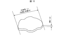
- FIG. 13 is a perspective view showing the shape of the conductive powder according to the first embodiment of the present invention.
- the conductive powder has a relatively uniform thickness in the thickness L2 direction.
- the conductive powder has a random shape in a plane perpendicular to the thickness direction.
- the length of the portion with the maximum delivery (width) is defined as the representative length L1 in the direction perpendicular to the thickness direction.
- the conductive powder has a distribution in both the representative length L1 and the thickness L2, in the following description, the median value is expressed numerically.
- the conductive powder has a thickness L1 of about 0.05 ⁇ m to 0.1 ⁇ m and a representative length L2 of about 5 ⁇ m to 10 ⁇ m.
- FIG. 14 is a diagram showing a result of a preliminary experiment on the conductive paste and the conductive powder contained in the electric conductor according to Embodiment 1 of the present invention.
- the maximum length of the conductive powder in the plane perpendicular to the thickness direction is the representative length.
- the mixture of spherical conductive powder having a diameter almost equal to the thickness of the conductive powder was satisfactory for both ejection and bonding.
- the thickness of the conductive powder when the alcohol component is 10% within a range of 0.05 ⁇ m to 0.1 ⁇ m and the representative length: 5 ⁇ m to 10 ⁇ m.
- the discharge shape and the bonding property are illustrated, it has been confirmed that the discharge shape and the bonding property are similarly excellent even when the alcohol component is in the range of 8% to 20%.
- the mixture containing the adhesive-based material could be discharged and the discharge shape could be made, but it collapsed when bonded. This is considered to be because dilatancy is not expressed.
- Discharge and bonding can be performed without problems with conductive powders (i) flat particles with a typical length of 5 ⁇ m and thickness of 0.1 ⁇ m, and (ii) flat particles with a typical length of 10 ⁇ m and thickness of 0.05 ⁇ m. It was.
- a conductive paste having a thickness of 0.05 ⁇ m or more and 0.1 ⁇ m or less and a thickness and a typical length of 5 ⁇ m to 10 ⁇ m was used and dispersed in an alcohol-based liquid component not containing an adhesive. It turns out that things are good.
- the alcohol-based liquid component is preferably 8% to 20% by weight.
- a conductive powder having a thickness of submicron has a large bond due to intermolecular force, and therefore the thickness of the conductive powder is preferably 0.1 ⁇ m or less.
- the conductive powder has a thickness of less than 0.05 ⁇ m, a stable conductive paste cannot be obtained unless the solvent is increased or a material that weakens the intermolecular force is used on the particle surface.
- the viscosity is too low to form a discharge shape, and the material that weakens the intermolecular force on the particle surface inhibits the expression of dilatancy, so it has not been a preferable material. Therefore, the thickness of the conductive powder is preferably 0.05 ⁇ m or more.
- a conductive paste is used in which silver particles (conductive powder) having a thickness of 0.08 ⁇ m and a representative length of 8 ⁇ m (thickness to representative length ratio of 100 times) are made of ethylene glycol having a weight ratio of 10%.
- the sintered silver paste sintered body shows good electric conduction, but in addition, in the case of mixing spherical particles having a diameter of 0.1 ⁇ m which is almost equal to the thickness, the spherical particles are present at the bonding interface between the flat particles. As a result, the electric conductivity is improved, and the value is 3.9 to 7.8 ⁇ ⁇ cm with respect to 2.1 ⁇ ⁇ cm of metallic silver, which is sufficiently higher than that of solder or the like. The same applies to heat conduction.
- a columnar body of the sintered silver paste is formed on the electrode pad of the circuit board with a dispenser (see FIG. 2).
- the semiconductor chip is sucked and fixed to the chip suction portion (bonding tool) of the flip chip bonder, the electrode pad of the semiconductor chip and the pad of the circuit board are aligned, and the distance between the semiconductor chip and the circuit board is set to a desired value. It is lowered until a load (reaction force) is applied to release the fixation of the chip adsorbing portion and to be fixed to the circuit board by its own weight.
- the reaction force of the chip monitored by the flip chip bonder behaves as shown in FIG.
- the reaction force increases due to the development of dilatancy (point C in FIG. 11). At that position, the chip suction is released and the chip is fixed by its own weight.
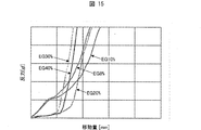
- FIG. 15 is a diagram showing the transition of load (reaction force) when mounting with a flip chip bonder with various alcohol-based liquid components.
- EG10% to EG40% shown in FIG. 15 represent the weight percentage of the alcohol-based liquid component (weight percentage of ethylene glycol).
- EG8%, EG10%, and EG20% show examples in which dilatancy was developed and bonding was possible.
- EG 30% and EG 40% show examples in which dilatancy is not expressed and the material is crushed during bonding.
- EG 20%, EG 30%, and EG40% behave in a similar manner, but the reaction force starts to rise.
- EG 30% and EG40% While the increase was due to the collapse, EG 20% was due to the fact that the deformation stopped with the development of dilatancy.
- EG8% and EG10% the reaction force increased again because the deformation stopped with the development of dilatancy.
- EG 8%, EG 10%, and EG 20% have slightly different behaviors, but EG 20% has a low viscosity, so that the stringing portion becomes longer and the deformation of the crushed portion becomes longer.
- bonding can be performed under load control by setting in advance a load at which deformation stops due to dilatancy.
- a thin film may be formed on the surface of the chip electrode of the semiconductor chip and the electrode pad surface of the circuit board for the purpose of preventing oxidation, but the description is omitted for the sake of simplicity. In addition, the effect of the effect due to the difference in their existence is small.
- connection portion electrical connection portion
- connection part completed as described above is composed only of a sintered silver paste that does not contain an adhesive, so it has excellent electrical and thermal conductivity and maintains mechanical properties even at high temperatures. It is.
- an electrode such as a protruding electrode can be obtained without being along the circuit board. Further, the distance between adjacent electrodes does not change, and the insulation between the electrodes is good.
- the sintered structure with many minute spaces which is a feature of the sintered silver paste, allows deformation and is superior to the pillar made of metal in all of the stress relaxation mechanism.
- the sintered silver paste when the sintered silver paste is sintered, it is necessary to volatilize the kneaded binder, but the surface area is reduced by making the sintered silver paste into many lumps and providing spaces between them. Since it becomes larger and the volatilization of the binder is completed in a shorter time, there is a secondary effect that the sintering is completed in a shorter time.
- FIG. 1 is a perspective view showing the structure of a sintered silver paste columnar body, circuit board, and semiconductor chip according to Embodiment 1 of the present invention.
- 100 is a semiconductor chip (element, electronic component), 101 is an electrode pad of the semiconductor chip, 200 is a circuit board (substrate), and 201 is an electrode pad of the circuit board 200.
- a conductive paste (conductive material) 202 is discharged and formed on the electrode pads 201 of the circuit board 200 with a dispenser. Thereby, the columnar conductive paste 202 is erected on the electrode pad 201 of the circuit board 200.
- a sintered silver paste was used as the conductive paste 202.
- the sintered silver paste used as the conductive paste 202 has a thickness of 0.05 ⁇ m or more and 0.1 ⁇ m or less, and the representative length is 5 ⁇ m or more and 10 ⁇ m when the maximum length in the plane perpendicular to the thickness is the representative length. It contains the following flat silver particles and ethylene glycol, does not contain an adhesive, and the weight ratio of the ethylene glycol is 8% or more and 20% or less of the conductive paste 202.
- the electrode pad 101 of the semiconductor chip 100 and the electrode pad 201 of the circuit board 200 are aligned, and further flip-chip connected, whereby the electrode pad 101 of the semiconductor chip 100 is connected to the circuit board 200.
- the top of the conductive paste 202 formed on the electrode pad 201 is contacted.
- the semiconductor chip 100 is mounted on the circuit board 200.
- the conductive paste 202 is drawn in a cylindrical shape for simplification of the drawing.
- a phenomenon called “stringing” causes a constricted and thinned portion due to the influence of the viscosity of the material, the movement of the nozzle, etc. even if the discharge is stopped. Cut out. Therefore, in practice, the upper portion of the conductive paste 202 has a conical shape.
- FIG. 2 is a diagram showing an example of the shape of the conductive paste formed by discharging with a dispenser.
- a “columnar” portion which is a lower portion of the conductive paste 202 shown in FIG. 2, is a portion in which the nozzle is raised at a constant speed while performing a constant discharge by a dispenser.
- the “thread-drawing” portion which is the upper portion of the conductive paste 202 shown in FIG. 2, is a portion in which the discharge of the dispenser is stopped and the nozzle is raised, and it has a conical shape depending on the viscosity of the conductive paste 202, the nozzle speed, etc. It is the part that was made by cutting the thinned part.
- the diameter of the base portion of the “stringing” portion was about 200 ⁇ m.
- FIG. 3 is a cross-sectional view of the circuit board 200 and the semiconductor chip 100 connected via the conductive paste 202 in a connected state.
- the electrode pad 201 of the circuit board 200 and the electrode pad 101 of the semiconductor chip 100 are aligned. Then, the semiconductor chip 100 was flip-chip connected to the circuit board 200 to electrically connect the electrode pad 101 and the electrode pad 201 via the conductive paste 202. Thereby, the electrical connection body (electrode connection structure) 1 was completed. Since the conductive paste 202 has high thermal conductivity, the electrode pad 101 and the electrode pad 201 are also thermally connected. That is, the conductive paste 202 functions as an electrical connection portion that electrically connects the electrode pad 101 and the electrode pad 201.
- FIG. 4 is a diagram illustrating an example of a method for forming the conductive paste 202 on the electrode pad 201 of the circuit board 200.
- the conductive paste 202 is ejected from a needle 203 at the tip of a syringe (not shown) of a dispenser (not shown) to form the conductive paste 202 on the electrode pad 201 of the circuit board 200.
- a product made by Musashi Engineering was used as the dispenser.
- the needle 203 As the needle 203, (i) an inner diameter of 100 ⁇ m—outer diameter of 200 ⁇ m, (ii) an inner diameter of 150 ⁇ m—outer diameter of 250 ⁇ m, and (iii) an inner diameter of 200 ⁇ m—outer diameter of 300 ⁇ m were used.
- the conductive paste 202 discharged by the needle 203 having an inner diameter of 100 ⁇ m is in a range of 100 ⁇ m to 110 ⁇ m in diameter, and (ii) the conductive paste 202 discharged by the needle 203 having an inner diameter of 150 ⁇ m has a diameter of 150 ⁇ m to 165 ⁇ m.
- the conductive paste 202 discharged by the needle 203 having an inner diameter of 200 ⁇ m was 200 ⁇ m to 220 m in diameter, and each finished in a cylindrical shape.
- the sintered silver paste discharged from the needle 203 stops being discharged at a desired height, and further, the needle 203 is pulled up to be naturally tapered and separated.
- the upper part of the conductive paste 202 has a conical shape called “stringer”.
- the cone angle can be controlled by the viscosity of the sintered silver paste and the pulling speed of the needle 203.
- the portion of the cone plays an important role in absorbing unevenness of the surface of the semiconductor chip 100 and the circuit board 200 (particularly, the circuit board 200), deviation in flatness such as waviness, and variation in the height of the formed conductive paste 202. Fulfill.
- the “stringer” portion When the needle 203 was raised at 5 mm / min after releasing the compressed air for discharge in the needle 203, the “stringer” portion was finished in a conical shape with a tip angle of 30 degrees. Further, when the needle 203 was raised at 10 mm / min, the tip angle of the “stringer” portion changed to 10 degrees. The tip angle of the “stringer” portion changes with the ascent speed of the needle 203, but the finished angle is stable.
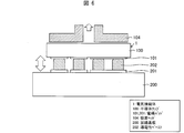
- FIG. 5 is a diagram illustrating a state in which the semiconductor chip 100 is suction fixed to the suction head 104 of a flip chip bonder (not shown) and the electrode pad 101 and the electrode pad 201 are aligned.
- the semiconductor chip 100 is fixed to the suction head 104 by vacuum suction from the suction hole of the suction head 104. Thereafter, the electrode pad 101 and the electrode pad 201 are aligned using a flip chip bonder mechanism.
- a flip chip bonder manufactured by Okuhara Electric was used.
- a flat collet that is slightly larger than the size of the semiconductor chip 100 having a vacuum suction hole with a diameter of 1 mm in the center was used, and the semiconductor chip 100 was sucked onto the flat collet. Thereafter, the electrode pad 101 of the semiconductor chip 100 and the electrode pad 201 of the circuit board 200 are recognized and aligned by a camera attached to a flip chip bonder, and the semiconductor chip 100 is moved to the circuit board 200 side.
- FIG. 5 is a diagram illustrating a state in which the semiconductor chip 100 is brought into contact with the electrode pad 101 and the conductive paste 202 by lowering the suction head 104 of a flip chip bonder (not shown) with respect to the circuit board 200. .
- the flip chip bonder there is a function of moving the suction head 104 based on reaction force information. With this function, the electrode pad 101 and the conductive paste 202 are brought into contact with each other while the conical portion of the “stringer” portion of the conductive paste 202 is crushed, leaving the cylindrical portion of the conductive paste 202. Can be relatively moved in the direction approaching the electrode pad 201 to determine the position.
- the vacuum suction of the suction head 104 is released, and the suction head 104 and the semiconductor chip 100 having the electrode pad 101 are separated, so that the electrode pad 101 is applied to the conductive paste 202 on the electrode pad 201 of the circuit board 200. It comes into contact.
- the load (reaction force) at this time is as shown in FIG. Details will be described later.
- the shape of the conductive paste 202 is maintained by the dilatancy, it is not necessary to pressurize the semiconductor chip 100 during firing.
- the solvent of the conductive paste 202 is volatilized, so that the conductive paste 202 is held at a temperature lower by 5 to 10 ° C. than the boiling point of the solvent.
- Complete sintering and return to ambient temperature As an example, the sintering was completed by maintaining the boiling point of the solvent at 197 ° C. at 190 ° C. for 15 minutes, and then increasing the sintering temperature to 250 ° C. and holding it for 30 minutes. Thereby, the electrical connection body 1 was completed.
- the conductive paste 202 is a sintered silver paste having a shape maintaining characteristic
- the conductive paste 202 which is a columnar protruding electrode that is self-supporting without being along the circuit board 200 or the semiconductor chip 100 is formed.
- the sintered silver paste which is the conductive paste 202
- the sintered silver paste is composed only of a sintered silver paste that does not contain an adhesive, it has excellent electrical and thermal conductivity, and mechanical properties even at high temperatures. Was to maintain.
- the horizontal cross-sectional shape (cross-sectional shape perpendicular to the extending direction of the conductive paste 202) is substantially the same shape, and the variation of the cross-sectional area is within 20%. there were.
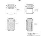
- FIG. 7 shows the shape of the needle 203 to be dispensed and the shape of the discharged conductive paste 202.
- 203-1 is a circular needle.
- the conductive paste becomes cylindrical as shown by the conductive paste 202-1.
- 203-2 is an example of a hexagonal needle.
- the conductive paste becomes hexagonal as shown in the conductive paste 202-2.
- an angle is formed on the inner side, but there is no particular problem because the angle is 120 degrees. In the case of a quadrangular needle, the inner corner is 90 degrees, so the corner ejection is not smooth.
- the discharge could be performed without any problem.
- the rounding of corners was doubled to 16 ⁇ m with respect to the maximum representative length of 8 ⁇ m of silver particles.
- the stability is preferably increased by 5 times 40 ⁇ m or more.
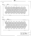
- FIG. 8 is a diagram showing an example in which needles are arranged in an array.
- FIG. 8A is a diagram showing an example in which circular needles 203-1 are arranged in an array
- FIG. 8B is a diagram showing an example in which hexagonal needles 203-2 are arranged in an array. It is.
- the electrodes are arranged in a six-sided close-packed state with the highest electrode density.
- the two-dot chain line in FIG. 8 conceptually shows the size of the nozzle of the dispenser, and arrangement is possible if the pitch is determined in consideration of the size of the nozzle and the alignment accuracy of the dispenser.
- the cross-sectional area that functions as an electrode increases and the connection resistance decreases.
- the surface area of the connecting portion is increased and the binder volatilization of the sintered silver paste can be performed smoothly, the sintering can be performed in a short time.
- a 1 mm ⁇ 0.5 mm electrode is entirely covered with sintered silver paste.
- the needles 203-1 and 203 are required.
- By arranging -2 in the form of an array it was possible to sinter sufficiently even if the preheating time was reduced from 30 minutes to 5 minutes.
- the horizontal cross-sectional shape of the plurality of columnar conductive pastes 202 is more reliably substantially the same shape, and The variation of the cross-sectional area could be within 20%.
- FIG. 9 shows a region between the electrode pad 101 and the electrode pad 201 with a resin material 205 after the electrode pad 101 and the electrode pad 201 are connected with the conductive paste 202. It is sectional drawing showing a mode that parts other than the connection part which are are filled.
- Sintered silver paste shows characteristics close to bulk silver in terms of electrical conduction and thermal conduction, but since it is a sintered body, mechanical properties, particularly malleability, do not become as good as those of metals. For this reason, the resistance to the repeated load of the connection portion has not reached that of metal bonding.
- the resin material 205 was filled in a part other than the sintered silver paste connection part, The reliability of the connecting part has increased, and sufficient reliability as a module has been demonstrated.
- the filled resin material 205 can use liquid epoxy or the like, and has the best reliability when the material is smaller than the Young's modulus of bulk silver and close to the thermal expansion coefficient of bulk silver.
- FIG. 10 shows an element or the like that requires a back contact.
- a connector (second substrate) 300 that connects the back electrode 207 of the semiconductor chip 100 and the electrode pad 201 of the circuit board 200 is connected to a plurality of conductive pastes ( It is sectional drawing showing a mode that it connects in the connection part which consists of (2nd electroconductive material) 204.
- the conductive paste 204 the same material as that of the conductive paste 202 was used.
- the conductive paste 204 is formed on the back electrode 207 with a dispenser and simultaneously on the desired electrode pad 201 of the circuit board 200.
- the conductive paste 202 is formed.
- the connector 300 is connected to the flip chip bonder, and the connector 300 is sucked, fixed, and pushed down, so that the connector 300 is connected to the conductive paste 204 on the back surface of the semiconductor chip 100 and the conductive paste 202 on the electrode pad of the circuit board 200.
- the functional pastes 204 and 202 are sintered. During the sintering, the conductive paste 202 that is already in contact with the electrode pad 101 on the surface of the semiconductor chip 100 does not change in its state due to the characteristics of the sintered silver paste.
- the semiconductor chip 100 is mounted with a flip chip bonder, and the conductive paste 204 is dispensed on the back surface of the semiconductor chip 100.
- the connector 300 is mounted using a flip chip bonder, and then all the conductive pastes 202 and 204 are fired. Since the sintered silver paste connecting portion has a shape retaining property, the shape of the connecting portion (conductive paste 202) on the surface side of the semiconductor chip 100 is maintained even when the connector 300 is mounted by a flip chip bonder. . Due to this property, the front and back can be connected simultaneously. In this way, a stack-connected electrical connection body (electrode connection structure) 1A was completed.
- FIG. 11 is a diagram showing the transition of the reaction force of the conductive pastes 202 and 204 when the semiconductor chip 100 adsorbed by the flip chip bonder is pushed down to the circuit board 200. Plotted by bonder chip movement and reaction force.
- the timing of pressing the semiconductor chip 100 and the connector 300 is controlled while monitoring the reaction force of the conductive paste 202/204.
- connection height can be controlled by the amount of sintered silver paste to be discharged.
- the conductive paste 202 is a conductive paste that can be used for electrical connection between a substrate (circuit board 200) and an electronic component (semiconductor chip 100) mounted on the substrate (circuit board 200).
- the conductive paste 202 includes a conductive powder and an alcohol-based liquid component, does not include an adhesive, and the conductive powder has a thickness of 0.05 ⁇ m or more and 0.1 ⁇ m or less, with respect to the thickness direction.
- the representative length is 5 ⁇ m or more and 10 ⁇ m or less, and the alcohol-based liquid component is a weight ratio in the conductive paste 202. Is 8% or more and 20% or less.
- the sintered silver paste formed from the conductive material is composed only of the sintered silver paste containing no adhesive, it is excellent in both electric conduction and heat conduction, and is mechanical even at high temperatures. Maintains the characteristics.
- the conductive paste 202 in aspect 1 is applied to the electrode pads 201 of the substrate (circuit board 200) and the electrodes of the electronic component (semiconductor chip 100).
- the electrical connection portion after the conductive paste that connects to the pad 101 is cured has a substantially cross-sectional shape perpendicular to the connection direction between the electrode pad 201 of the substrate (circuit substrate 200) and the electronic component (semiconductor chip 100). The variation may be within 20% in the cross-sectional area with the same shape.
- the manufacturing method of the electrode connection structure (electrical connection body 1) according to the third aspect of the present invention is the manufacturing method of the electrode connection structure according to the second aspect, in which the conductive material is formed on the electrode pad 201 of the substrate (circuit board 200).
- Forming a protruding electrode with the conductive paste 202 and bringing the electrode pad 101 of the electronic component (semiconductor chip 100) into contact with the protruding electrode on the electrode pad 201 of the substrate (circuit substrate 200) When the electrode pad 101 of the chip 100) is relatively moved in a direction approaching the electrode pad 201 of the substrate (circuit board 200) at a constant speed and a reaction force of a predetermined value is received from the protruding electrode, the electronic component ( The step of stopping the relative movement of the electrode pad 101 of the semiconductor chip 100) and the movement of the electrode pad 101 of the electronic component (semiconductor chip 100).
- the electrode pads 201 of the said substrate (circuit board 200) may include
- Electrode connection structure 100 Semiconductor chips (elements, electronic components) 101, 201 Electrode pad 104 Suction head 200 Circuit board (substrate) 202 Conductive paste (projection electrode) 203 Needle 204 Conductive paste (projection electrode) 205 Resin material 207 Back electrode 300 Connector (second substrate)
Landscapes
- Engineering & Computer Science (AREA)
- Chemical & Material Sciences (AREA)
- Manufacturing & Machinery (AREA)
- Physics & Mathematics (AREA)
- Materials Engineering (AREA)
- Mechanical Engineering (AREA)
- Composite Materials (AREA)
- Dispersion Chemistry (AREA)
- Spectroscopy & Molecular Physics (AREA)
- Nanotechnology (AREA)
- Microelectronics & Electronic Packaging (AREA)
- Wire Bonding (AREA)
- Conductive Materials (AREA)
- Electric Connection Of Electric Components To Printed Circuits (AREA)
Abstract
基板に自立する突起電極のような電極を得る。導電性ペースト(202)は、導電粉末とアルコール系液体成分とを含み、接着剤を含まず、前記導電性粉末は、厚さが0.05μm以上0.1μm以下であり、当該厚さ方向に垂直な面内の最大の差し渡しである代表長さが5μm以上10μm以下である導電粒子を含み、前記アルコール系液成分は、前記導電性ペーストに対する重量比が、8%以上20%以下である。
Description
本発明は、フリップチップ接続構造およびその実現方法に関する。特にダイラタンシー性を持つ導電性ペーストと、それを用いた電気接続構造およびその製造方法に関する。
フリップチップ接続に導電性ペーストを用いようとする試みは、多く行われてきた。特にサブミクロンの導電性微粒子を用いた焼結型導電性ペーストを使った接合では、硬化後に導電性材料のバルク銀並の温度特性、機械的特性を持つようになることから、接合部が高温に耐えることができることが期待できる。そのため、高温動作するデバイスの接合部に使える可能性があるため、近年、注目される技術となっている。
http://www.stat.phys.kyushu-u.ac.jp/~nakanisi/Physics/Dilatancy/
特許文献1に開示される焼結型銀ペーストは、2種類の銀粒子を、接着剤を含まないバインダに分散したもので、硬化後の特性として、バルク銀に近い特性を持つものである。この特許文献1に開示される内容は、広い面積に塗布して電子デバイスを搭載、加圧状態で硬化させるものである。特許文献1に開示された内容は、広い面積に塗布することから、電子デバイスの電極接続には技術が及んでいなかった。
一方、特許文献2には、電子デバイスの電極と回路基板の電極を接続する方法が開示されている。図12を用いて、特許文献2に開示された、電子デバイスの電極と回路基板の電極を接続する方法を説明する。
図12において、100は半導体チップ、101は半導体チップの電極パッド、200は回路基板、201は回路基板の電極パッドである。回路基板200には、半導体チップ100の側面を覆うように隆起部220が形成され、電極バッド101から隆起部220の表面を通り、電極パッド201に向かって焼結型銀ペースト221が配置されている。
焼結型銀ペースト221に流動性があるため、隆起部220は、焼結型銀ペースト221の途中経路を維持させるために設けられている。焼結型銀ペースト221の途中経路を維持させるため回路基板200に沿わせる必要があり、自由度としては制限を受けるものであった。また、このような構造では、焼結型銀ペースト221の断面形状が不安定なものになり、材料自体の電気伝導、熱伝導の優れる特性が十分に発揮できないものであった。
本発明は、前記の問題点に鑑みてなされたものであり、その目的は、自立する突起電極のような電極を形成できる導電性ペーストを得ること、及び、導電性ペーストを使って電極間を接続することである。
上記の課題を解決するために、本発明の一態様に係る導電性ペーストは、基板と該基板上に搭載される電子部品との間の電気接続に使用可能な導電性ペーストであって、導電粉末とアルコール系液体成分とを含み、接着剤を含まず、前記導電粉末は、厚さが0.05μm以上0.1μm以下であり、当該厚さ方向に対して垂直に交わる面内の最大の差し渡しを代表長さのとしたとき、当該代表長さが5μm以上10μm以下である導電粒子を含み、前記アルコール系液体成分は、前記導電性ペーストにおける重量比が、8%以上20%以下であることを特徴とする。
本発明の一態様によれば、自立する突起電極のような電極を得ることができ、かつ、導電性ペーストを使って電極間を接続するという効果を奏する。
〔実施形態1〕
(導電性ペースト及び電気導電体の概略)
以下、本発明の実施の形態について、詳細に説明する。本実施形態に係る電気接続体では、基板と、該基板上に搭載される電子部品との間の電気接続に導電性ペーストとして形状保持性が高いものを用いる。そして、導電性ペーストをディスペンサで吐出し、その形状を維持した状態で焼結させる。これにより、電気接続体を得る。具体的には、導電性ペーストとしてダイラタンシー性をもったものを使用する。
(導電性ペースト及び電気導電体の概略)
以下、本発明の実施の形態について、詳細に説明する。本実施形態に係る電気接続体では、基板と、該基板上に搭載される電子部品との間の電気接続に導電性ペーストとして形状保持性が高いものを用いる。そして、導電性ペーストをディスペンサで吐出し、その形状を維持した状態で焼結させる。これにより、電気接続体を得る。具体的には、導電性ペーストとしてダイラタンシー性をもったものを使用する。
ダイラタンシー性とは、非ニュートン流体の一種が持つ性質で、ずり速度の増加に対して、粘度が増加するというものである。小さな粒子が液体に混合されたものでよく発現する性質である。例としては、乾燥した砂の上に重量物を乗せると沈むが、砂が水を含んで湿っていると重量物を乗せても少し沈むだけでそれ以降は沈まない。ずり速度が変形によって上昇することから、ダイラタンシー性が発現するずり速度に達して粘度が上昇、変形が止まってしまったように見えたと考えられる。さらに、特徴的な現象として、変形した部分の砂は乾燥しているように見える。最密充填に近い状態から変形させようとすると、粒子間が逆に拡大し、その空間に水が移動したため、変形した部分は乾燥してくるのである(非特許文献1参照)。
このようなダイラタンシー性の性質をもつ材料からなる導電性ペーストを使い、回路基板の所望の電極上にディスペンサなどで吐出させることで、所望の形状の硬化前の導電性ペーストの上方部分に突起形状部分を作る。
その後、導電性ペーストにおける突起形状部分に対して、素子電極を位置合わせして素子電極を導電性ペーストにおける突起形状部分に押し当てる。導電性ペーストにおける突起形状部分に押し当て、導電性ペーストが変形に伴い、ずり速度が上昇、その結果、導電性ペーストのダイラタンシー性が発現するずり速度に達し、変形に対して反力が増加に転じる。ちょうど、濡れた砂が少し沈む(変形する)とダイラタンシー性で急激に変形しにくくなることのアナロジーである。
ダイラタンシーによって、変形した部分が乾くことは、焼結型導電性ペーストに対して好都合である。バインダが局所的に少なくなることで、導電粒子間が接触するため、粒子間の分子間力による結合が局所的に起こる。そのため、仮接合したような状態になると考えられる。
ダイラタンシー性のポイントとなる導電粉末の形状について、図13を用いて説明する。図13は、本発明の実施形態1に係る導電粉末の形状を表す斜視図である。
図13に示すように、1つの導電性粉末についてみると、導電粉末は、厚さL2方向に比較的均一な厚さをもっている。導電粉末は、厚さ方向に垂直な平面内では、ランダムな形状である。導電粉末において、先渡し(幅)の最大になる部分の長さをもって、厚さ方向に垂直な方向の代表長L1とする。
導電粉末は、代表長L1、厚さL2とも、分布をもっているので、以下の説明では、メジアン値をもって数値表現している。導電粉末は、厚さL1は0.05μm以上0.1μm以下程度であり、代表長さL2は5μm以上10μm以下程度である。
図14は、本発明の実施形態1に係る導電性ペースト及び電気導電体に含まれる導電粉末に関する予備実験の結果を表す図である。
上述のように、導電粉末における、厚さ方向に垂直な面における先渡しの最大長さを代表長さとする。
代表長さ8μmで厚さ0.08μmの導電粉末を使い、アルコール系液体成分の量、同時に混合する球形粒子有無、接着剤系バインダを変えながら、ディスペンサによる吐出状態とボンディングの結果を確認する実験を行った。アルコール系液体成分は、エチレングリコール、接着剤系材料はエポキシ樹脂を用いた。アルコール系液体成分は、5%では粘度が高くなりすぎ吐出ができなかった。一方、アルコール系液体成分が40%では粘度が低く形状を保つことができなかった。アルコール系液体成分が30%では吐出は何とかできたが、ダイラタンシー性が発現するまでに吐出した導電性ペーストが潰れてしまった。アルコール系液体成分は8%以上20%以下が良好な吐出とボンディングが実現できた。
導電粉末の厚さとほぼ等しい径をもつ球形の導電粉末を混合したものも、吐出、ボンディングとも問題無かった。
さらに、図14では、球形粒子:有について、アルコール系成分が10%の時の導電性粉末の厚さ:0.05μm以上0.1μm、及び、代表長さ:5μm以上10μm以下の範囲内での吐出形状およびボンディング性を図示したが、アルコール系成分を8%以上20%以下の範囲内としても同様に吐出形状およびボンディング性が優れることは確認済である。
一方、接着剤系材料も混合したものは、吐出させることができ、吐出形状を作ることができたものの、ボンディングすると潰れてしまった。これは、ダイラタンシー性が発現できていないためであると考えられる。
導電粉末である、(i)代表長さ5μmで厚さ0.1μmの扁平粒子、(ii)代表長さ10μm、厚さ0.05μmの扁平粒子とも、吐出、ボンディングは問題なく行うことができた。
しかし、厚さ0.03μmの導電粉末を用いたものでは、材料の活性化が高まり、保護コートを強化せざるをえず、そのため、吐出形状を何とか作ることができたものの、ダイラタンシー性が発現せず、ボンディングの際に潰れてしまった。
また、0.2μmの厚さの導電粉末でも、ダイラタンシー性が発現せず、ボンディングの際に潰れてしまった。
結果、導電性ペーストとしては、厚さが0.05μm以上0.1μm以下で、厚さと代表的長さは5μm~10μmの導電粉末を使い、接着剤を含まないアルコール系液体成分に分散させたものが、良いということが分かった。アルコール系液体成分は、重量比で8%以上20%以下が好ましい。
導電粉末として、厚さがサブミクロンにあるものが、分子間力による結合が大きいため、導電粉末の厚さとしては0.1μm以下がよい。
ただし、厚さが0.05μmより小さい導電粉末では、溶剤を多くするか、粒子表面に分子間力を弱める材料を用いないと安定な導電性ペーストを得ることができず、溶剤を多くすることで粘度が下がり過ぎ、吐出形状が作れない、また、粒子表面の分子間力を弱める材料がダイラタンシー性の発現を阻害することから、好ましい材料にはならなかった。よって、導電粉末の厚さは0.05μm以上がよい。
そして、導電粉末を溶かす溶液成分としては、アルコール系液体成分のみを使う。接着剤などの高分子材料を添加すると、やはりダイラタンシー性の発現を阻害してしまった。
本実施形態では、厚さ0.08μm、代表長さ8μm(厚さと代表長さの比100倍)の銀粒子(導電粉末)を重量比10%のエチレングリコールで作った導電性ペーストを用い、ディスペンサで導電性ペーストを吐出後、そのまま硬化(焼結)すると、吐出形状をほぼ維持する形で焼結が完了する。
焼結した銀ペースト焼結体は、良好な電気伝導を示すが、さらに、厚さとほぼ等しい0.1μm径の球形粒子を混合したものは、球形粒子が、扁平粒子間の接合界面に介在することで、より電気伝導が良くなり、金属銀の2.1μΩ・cmに対して、3.9~7.8μΩ・cmの値をもっており、半田等に比べ十分に高い値を示す。熱伝導も同様である。
該焼結型銀ペーストを用いて回路基板の電極パッド上に該焼結型銀ペーストの柱状体をディスペンサで形成する(図2参照)。
続いて、半導体チップをフリップチップボンダーのチップ吸着部(ボンディングツール)に吸着固定し、該半導体チップの電極パッドと回路基板のパッドとを位置合わせして、半導体チップと回路基板の間隔を所望の荷重(反力)がかかるまで下げて、チップ吸着部の固定を解放、回路基板に半導体チップの自重だけて固定されるようにする。フリップチップボンダーが監視(モニター)しているチップの反力は、図11のようにふるまう。フリップチップボンダーで半導体チップの移動速度を所定の速度で一定に保ちつつ回路基板に押し下げていくと、ダイラタンシー性の発現によって、反力が高まる点がでる(図11のC点)。その位置でチップ吸着を解放、チップ自重で固定されるようにする。
図15は、各種アルコール系液体成分でのフリップチップボンダーでの搭載時の荷重(反力)推移を表す図である。図15に示すEG10%~EG40%は、アルコール系液体成分の重量パーセント(エチレングリコールの重量パーセント)を表している。
EG8%、EG10%、及び、EG20%は、ダイラタンシー性が発現しボンディングできた例を示している。
一方、EG30%とEG40%とは、ダイラタンシー性が発現せず、ボンディングの際に潰れてしまった例を示している。
反力の経過としては、EG 20%、EG 30%、及び、EG40%は似た振舞をするが、反力が上昇し始める点は、EG 30%とEG40%とは導電性ペーストが完全に潰れたことによる上昇であるのに対して、EG20%はダイラタンシー性の発現に伴い変形が止まったことによるものであった。EG8%、及び、EG10%も同じく、反力が再び上昇する点はダイラタンシー性の発現に伴い変形が止まったことによるものであった。
EG8%、EG10%、及び、EG20%は、挙動が少し異なるが、EG20%では、粘度が低いため、糸引き部分がながくなり、それを潰す分の変形が長くなったのである。
この結果より、ダイラタンシー性を持つ導電性ペーストを使うと、ダイラタンシー性で変形が止まる荷重を予め設定することで、荷重制御でボンディングが可能であることが分かる。
その後、焼結型銀ペーストを焼結させることで、焼結型銀ペーストだけで接続された半導体チップと回路基板の接続が実現できる。
このようにすることで、ディスペンサで吐出した形状を維持したまま、焼結され、ピラー接続と同様の電気接続部の形状ができあがる。
なお、半導体チップのチップ電極表面、回路基板の電極パッド表面に酸化防止などの目的で薄い膜が形成されることがあるが、簡単化のためにその説明を割愛している。また、それらの存在の差異による効果の影響は小さい。
(主な利点)
ここで、以下の説明では、半導体チップと回路基板とを接続する導電性ペーストを接続部(電気接続部)と称する場合がある。
ここで、以下の説明では、半導体チップと回路基板とを接続する導電性ペーストを接続部(電気接続部)と称する場合がある。
上述のようにして出来上がった接続部は、接着剤を含まず焼結した銀ペーストのみから構成されるため、電気伝導、熱伝導ともに優れるものであり、また高温においても機械的特性を維持するものである。
焼結型銀ペーストにおける形状維持性よって、回路基板に沿わせることなく、突起電極のような電極とすることができる。さらに隣接する電極との間隔は変わることがなく、電極間の絶縁性が良好である。
また、焼結型銀ペーストの特徴である微小な空間の多い焼結構造は、変形を許し応力緩和機構がすべて金属でできたピラーよりも優れるものになる。
加えて、焼結型銀ペーストを焼結させる際に、混錬したバインダを揮発させることが必要になるが、焼結型銀ペーストを多数の塊とし、間に空間を設けることで、表面積が大きくなり、バインダの揮発がより短時間で完了することから、焼結がより短時間に完成する副次効果がある。
〔実験例〕
図1~図11を用いて、本発明の実施形態1に係る実験例について説明する。
図1~図11を用いて、本発明の実施形態1に係る実験例について説明する。
図1は本発明の実施形態1に係る焼結型銀ペーストの柱状体、回路基板、及び、半導体チップの構造を表す斜視図である。
図1において、100は半導体チップ(素子、電子部品)、101は半導体チップの電極パッド、200は回路基板(基板)、201は回路基板200の電極パッドである。回路基板200の電極パッド201上に導電性ペースト(導電性材料)202をディスペンサで吐出し形成する。これにより、回路基板200の電極パッド201上に柱状の導電性ペースト202を立てる。
本実験例では、導電性ペースト202として、焼結型銀ペーストを用いた。導電性ペースト202として用いた焼結型銀ペーストは、厚さが0.05μm以上0.1μm以下で厚さと垂直な面内の最大の先渡しを代表長さとしたとき、代表長さが5μm以上10μm以下の扁平状の銀粒子と、エチレングリコールとを含み、接着剤を含まず、上記エチレングリコールの重量割合は、導電性ペースト202の8%以上20%以下である。
そして、この状態で、半導体チップ100の電極パッド101と、回路基板200の電極パッド201とを位置合わせして、さらに、フリップチップ接続することで、半導体チップ100の電極パッド101を、回路基板200の電極パッド201上に形成されている導電性ペースト202の頭頂部に接触させる。これにより、半導体チップ100を、回路基板200上に搭載する。なお、図1では、導電性ペースト202を図の簡単化のため円柱状に描画している。しかし、実際は、導電性ペースト202のディスペンスの際に「糸ひき」と呼ばれる現象によって、吐出を停止しても材料の粘度、ノズルの移動等の影響によって円錐状に伸びて、細くなった部分で切れる。そのため、実際には、導電性ペースト202における上方部分は円錐形になる。
図2は、ディスペンサで吐出し形成した導電性ペーストの形状例を表す図である。図2に示す、導電性ペースト202の下方部分である「円柱状」部分は、ディスペンサによって一定の吐出を行いながら、ノズルを一定速度で上昇させた部分である。図2に示す、導電性ペースト202の上方部分である「糸引き」部分は、ディスペンサの吐出を止めて、ノズルを上昇させた部分であり、導電性ペースト202の粘度、ノズル速度等によって円錐状となり、細くなった部分で切れたことでできた部分である。「糸引き」部分の基部の直径は200μm程度であった。
図3は、導電性ペースト202を介して接続した回路基板200と半導体チップ100との接続状態での断面図である。
図3に示すように、回路基板200の電極パッド201と、半導体チップ100の電極パッド101を位置合わせする。そして、半導体チップ100を、回路基板200にフリップチップ接続することで、導電性ペースト202を介して電極パッド101と電極パッド201を電気的に接続した。これにより、電気接続体(電極接続構造)1が完成した。導電性ペースト202は、熱伝導性も高いため、電極パッド101と、電極パッド201とは熱的にも接続される。すなわち、導電性ペースト202は、電極パッド101と、電極パッド201とを電気的に接続する電気接続部として機能する。
図4は、回路基板200の電極パッド201上に、導電性ペースト202を形成する方法の例を示す図である。
図4に示すように、ディスペンサ(図示せず)のシリンジ(図示せず)先端のニードル203から導電性ペースト202を吐出し、回路基板200の電極パッド201上に、導電性ペースト202を形成する。本実験例では、ディスペンサとして、ムサシエンジニアリング製のものを用いた。また、ニードル203としては、(i)内径100μm-外形200μmのもの、(ii)内径150μm‐外形250μmのもの、(iii)内径200μm‐外形300μmのもの、を用いた。
焼結型銀ペーストの特性から、ディスペンサのニードル203から吐出されると、導電性ペースト202は形状がそのまま維持される。(i)内径100μmのニードル203にて吐出した導電性ペースト202は直径100μm~110μmの範囲で、(ii)内径150μmのニードル203にて吐出した導電性ペースト202は直径150μm~165μmで、(iii)内径200μmのニードル203にて吐出した導電性ペースト202は直径200μm~220mで、それぞれ円柱状に出来上がった。
上記(i)~(iii)の各ニードル203にて吐出した導電性ペースト202をそのまま焼結したところ、それぞれの導電性ペースト202の直径の収縮は10μm以内であり、形状がそのまま維持された状態で焼結された。
ニードル203から吐出した焼結型銀ペーストは、所望の高さで吐出を止め、さらに、ニードル203を引き上げることで、自然と先細になり切り離される。導電性ペースト202の上方部分は「糸ひき」と呼ばれる錐状になる。錐の角度は焼結型銀ペーストの粘度と、ニードル203の引き上げ速度で制御できる。錐の部分は、半導体チップ100、回路基板200(特に回路基板200)の表面の凹凸、うねりなどの平面性のずれ、形成した導電性ペースト202の高さばらつきを吸収するために重要な役割を果たす。
ニードル203において、吐出のための圧縮空気を解放したあと、ニードル203を5mm/minで上昇させると、「糸ひき」部分は、先端角度30度の円錐形状に仕上がった。また、ニードル203を10mm/minで上昇させると、「糸ひき」部分は、先端角度が10度に変化した。ニードル203の上昇速度で、「糸ひき」部分の先端角度は変わるが、仕上がる角度は安定していた。
図5は、半導体チップ100をフリップチップボンダー(図示せず)の吸着ヘッド104に吸着固定し、電極パッド101と、電極パッド201とをアライメントしている様子を表す図である。吸着ヘッド104の吸着穴から真空吸着によって、半導体チップ100は吸着ヘッド104に固定される。その後、フリップチップボンダーの機構を使い電極パッド101と電極パッド201とをアライメントする。
フリップチップボンダーとしては、奥原電気製のものを用いた。中央に直径1mmの真空吸着穴を持つ半導体チップ100の大きさに対して若干大きい平コレットを用い、平コレットに半導体チップ100を吸着した。その後、フリップチップボンダーにつけたカメラで半導体チップ100の電極パッド101、回路基板200の電極パッド201を認識、位置合わせして半導体チップ100を回路基板200側に動かす。
図5は、半導体チップ100を、回路基板200に対してフリップチップボンダー(図示せず)の吸着ヘッド104を下げて電極パッド101と導電性ペースト202とを接触させている様子を表す図である。フリップチップボンダーの機能として、吸着ヘッド104を、反力情報をもとに動かす機能がある。この機能によって、導電性ペースト202の「糸ひき」部分の円錐状部を潰しながら、電極パッド101と導電性ペースト202とを接触させ、導電性ペースト202の円柱状部分を残す形で電極パッド101を電極バッド201に近づく方向に相対移動させて位置を決めることができる。その後、吸着ヘッド104の真空吸着を解除して、吸着ヘッド104と電極パッド101を有する半導体チップ100とを離すことで、電極パッド101は、回路基板200の電極パッド201上の導電性ペースト202に接触した状態となる。この時の荷重(反力)は図11に示すようになった。詳細は後述する。
図6に示すように、電極パッド101が導電性ペースト202の接続部である「糸引き」部分に接触し始めると、徐々に反力が上昇、その後、一度反力の上昇が緩やかになった後、上昇し始める。
反力が再上昇し始めた値を狙って、その反力値に達した時に吸着ヘッド104を止めて、半導体チップ100を吸着ヘッド104から解放し、その後、半導体チップ100の自重で電極パッド101が導電性ペースト202と接触を保つ状態で系全体を加熱し、導電性ペースト202を焼成する。これにより、導電性ペースト202と電極パッド101との接続が完了する。
導電性ペースト202はダイラタンシー性によって形状が維持されているので、焼成時は半導体チップ100を加圧する必要はない。
導電性ペースト202の硬化は、まず、導電性ペースト202の溶媒を揮発させるため、溶媒の沸点より5~10℃低い温度で保持し、その後、銀ペーストを焼結させる温度に上昇、保持して焼結を完了させ常温に戻す。例としては、溶媒の沸点197℃に対して190℃で15分保持、その後、焼結温度である250℃に上昇させて30分保持することで焼結が完了した。これにより、電気接続体1が完成した。
このように、導電性ペースト202は、形状維持特性を有する焼結型銀ペーストであるため、回路基板200や半導体チップ100に沿わせることなく自立する柱状の突起電極である導電性ペースト202を形成することができた。さらに、導電性ペースト202である焼結型銀ペーストは、接着剤を含まず焼結した銀ペーストのみから構成されるため、電気伝導、熱伝導ともに優れるものであり、また高温においても機械的特性を維持するものであった。
また、前記接続部を構成する柱状の導電性ペースト202において、水平断面形状(導電性ペースト202の延伸方向に垂直な断面形状)は互いに略同一形状であり、断面積の変動が20%以内であった。
図7は、ディスペンスするニードル203の形状と吐出された導電性ペースト202の形状を示す。203‐1は円形のニードルである。円形のニードル203‐1から吐出させると、導電性ペースト202‐1に示すように、導電性ペーストは円柱状になる。203-2は六角形にしたニードルの例である。六角形のニードル203‐2から吐出させると、導電性ペースト202‐2に示すように導電性ペーストは六角形になる。また、六角形のニードル203‐2から吐出させると内側に角がつくが、120度であるので特に問題なかった。四角形にしたニードルの場合、内側の角が90度になるので、角の吐出がスムーズでなくなった。導電性ペースト202の導電粒子の代表長さよりも大きい円弧状に角を丸めることで吐出が問題なく行えた。具体的には、銀粒子の代表長さの最大8μmに対して、角の丸めを2倍の16μmとした。また好ましくは5倍の40μm以上の方が、安定性が増した。
〔実施形態2〕
図8はニードルをアレイ状に並べた例を示す図である。図8の(a)は円形のニードル203‐1をアレイ状に並べた例を示す図であり、図8の(b)は六角形のニードル203‐2をアレイ状に並べた例を示す図である。
図8はニードルをアレイ状に並べた例を示す図である。図8の(a)は円形のニードル203‐1をアレイ状に並べた例を示す図であり、図8の(b)は六角形のニードル203‐2をアレイ状に並べた例を示す図である。
大きな面積の電極に対しては、ニードルをアレイ状に配列する。図8の例は、最も電極の密度が高くなる6方最密状に並べたものである。
図8中の2点鎖線は、ディスペンサのノズルの大きさを概念的にしめしており、ノズルの大きさとディスペンサの位置合わせ精度を勘案して、ピッチを決めれば、配列は可能である。
このようにすることで、電極として機能する断面積が増え、接続抵抗が下がる。一方、接続部の表面積が増え、焼結型銀ペーストのバインダ揮発がスムーズに行えるようになるため、焼結が短時間で行えるようになった。
例えば、図8の(a)(b)にしめすようなアレイ状になっていないニードル203‐1・203-2で、1mm×0.5mmの電極に対して、全面を焼結型銀ペーストで接続するには、30分のプリヒートを行って、バインダを揮発、その後30分の焼結を行う必要があったが、図8の(a)(b)に示すようにニードル203‐1・203-2をアレイ状に配置することでプリヒート時間は30分から5分に短縮しても十分に焼結できた。
また、このように、ニードル203‐1・203-2をアレイ状に配置することで、複数本の柱状の導電性ペースト202の水平断面形状を、より確実に、略同一形状であり、かつ、断面積の変動を20%以内とすることができた。
〔実施形態3〕
図9は、導電性ペースト202で電極パッド101と電極パッド201とを接続した後、樹脂材料205にて、電極パッド101と電極パッド201との間の領域であって、複数の導電性ペースト202である接続部以外の部分を充填した様子を表す断面図である。
図9は、導電性ペースト202で電極パッド101と電極パッド201とを接続した後、樹脂材料205にて、電極パッド101と電極パッド201との間の領域であって、複数の導電性ペースト202である接続部以外の部分を充填した様子を表す断面図である。
焼結型銀ペーストは、電気伝導、熱伝導に関してはバルク銀に近い特性を示すが、焼結体であるため、機械特性、特に展性は金属ほどの特性にはならない。そのため、接続部の繰り返し荷重に対する耐性は金属接合ほどには至らなかった。しかし、最初の接続、その後、数回のリペア―などの温度履歴では接続は問題なかったので、最終の動作確認後に、樹脂材料205を焼結型銀ペースト接続部以外の部分に充填したところ、接続部の信頼性が高まり、モジュールとして十分な信頼性を発揮できた。充填した樹脂材料205は、液状エポキシなどが使え、バルク銀のヤング率より小さく、かつ、バルク銀の熱膨張係数に近い材料の時に信頼性が最もよくなった。
〔実施形態4〕
図10は、バックコンタクトを必要とする素子などで、半導体チップ100の裏面電極207と、回路基板200の電極パッド201とを接続する接続子(第2基板)300を、複数の導電性ペースト(第2導電性材料)204からなる接続部で接続している様子を表す断面図である。導電性ペースト204も導電性ペースト202と同様の材料を用いた。
図10は、バックコンタクトを必要とする素子などで、半導体チップ100の裏面電極207と、回路基板200の電極パッド201とを接続する接続子(第2基板)300を、複数の導電性ペースト(第2導電性材料)204からなる接続部で接続している様子を表す断面図である。導電性ペースト204も導電性ペースト202と同様の材料を用いた。
半導体チップ100の表面の電極パッド101に対して、導電性ペースト202で接続、焼結後、裏面電極207上に、ディスペンサで導電性ペースト204を形成、同時に回路基板200の所望の電極パッド201上にも、導電性ペースト202を形成する。これにより、柱状であって複数の導電性ペースト204を裏面電極207上に立て、柱状であって複数の導電性ペースト202を電極パッド201上に立てた。
その後、フリップチップボンダーに接続し300を吸着固定して押し下げることで、接続子300を、半導体チップ100裏面の導電性ペースト204、回路基板200の電極パッド上の導電性ペースト202に接続し、導電性ペースト204・202を焼結させる。この焼結の際に、すでに焼結されている、半導体チップ100表面の電極パッド101と接触している導電性ペースト202は、焼結型銀ペーストの特性から、その状態に変化が生じない。
また、この場合、焼結を、半導体チップ100の表面、裏面双方の導電性ペースト202・204からなる接続部に対して同時に行うことも可能である。
まず、回路基板200の電極パッド201上に導電性ペースト202を全て形成する。
次に、半導体チップ100をフリップチップボンダーで搭載し、半導体チップ100の裏面に、導電性ペースト204をディスペンスする。続いて接続子300をフリップチップボンダーで搭載し、その後、全ての導電性ペースト202・204を焼成する。焼結型銀ペースト接続部は、その形状保持性から、接続子300をフリップチップボンダーで搭載する際も、半導体チップ100表面側の接続部(導電性ペースト202)は形状が保持されたままである。この性質により、表裏の接続を同時に行うことができる。このようにして、スタック接続された電気接続体(電極接続構造)1Aが完成した。
〔実施形態5〕
図11は、フリップチップボンダーに吸着させた半導体チップ100を回路基板200に押し下げていった時の、導電性ペースト202・204の反力の推移を示す図である。ボンダーのチップ移動量と反力でプロットしている。
図11は、フリップチップボンダーに吸着させた半導体チップ100を回路基板200に押し下げていった時の、導電性ペースト202・204の反力の推移を示す図である。ボンダーのチップ移動量と反力でプロットしている。
図11に示すように、導電性ペースト202・204の反力をモニターしながら、半導体チップ100及び接続子300を押し当てるタイミングを制御する。
半導体チップ100を押し下げていくと、焼結型銀ペーストの「糸引き」の先端にチップの電極が接触するまでは、反力が生じない。A点で「糸引き」の先端とチップの電極が接触し、反力が徐々に増加し、B点に到達し糸引き部分が全て潰れ、断面積の増加がなくなるため、ダイラタンシー性が発現しない移動速度では、反力の上昇が緩やかになる。そのまま押し下げていくと、C点で反力が増加し始める。これは、材料のダイラタンシー性が発現し反力が上昇していると考えられる。
この反力の振舞から、フリップチップ時は、ダイラタンシー性で反力が高まった点の反力の値をもって止まるように制御すれば、接続は安定的に行えることが分かる。接続高さの制御は、吐出させる焼結型銀ペーストの量で行える。
〔まとめ〕
本発明の態様1に係る導電性ペースト202は、基板(回路基板200)と該基板(回路基板200)上に搭載される電子部品(半導体チップ100)との間の電気接続に使用可能な導電性ペースト202であって、導電粉末とアルコール系液体成分とを含み、接着剤を含まず、前記導電性粉末は、厚さが0.05μm以上0.1μm以下であり、当該厚さ方向に対して垂直に交わる面内の最大の差し渡しを代表長さのとしたとき、当該代表長さが5μm以上10μm以下である導電粒子を含み、前記アルコール系液成分は、前記導電性ペースト202における重量比が、8%以上20%以下であることを特徴とする。
本発明の態様1に係る導電性ペースト202は、基板(回路基板200)と該基板(回路基板200)上に搭載される電子部品(半導体チップ100)との間の電気接続に使用可能な導電性ペースト202であって、導電粉末とアルコール系液体成分とを含み、接着剤を含まず、前記導電性粉末は、厚さが0.05μm以上0.1μm以下であり、当該厚さ方向に対して垂直に交わる面内の最大の差し渡しを代表長さのとしたとき、当該代表長さが5μm以上10μm以下である導電粒子を含み、前記アルコール系液成分は、前記導電性ペースト202における重量比が、8%以上20%以下であることを特徴とする。
前記構成によると、形状維持特性を有する焼結型銀ペーストである導電性材料を得ることができる。このため、前記基板に自立する突起電極のような電極を前記導電性材料から形成することができる。さらに、前記導電性材料から形成した焼結型銀ペーストは、接着剤を含まず焼結した銀ペーストのみから構成されるため、電気伝導、熱伝導ともに優れるものであり、また高温においても機械的特性を維持するものである。
本発明の態様2に係る電気接続構造(電気接続体1)は、前記態様1における導電性ペースト202を、前記基板(回路基板200)の電極パッド201と前記電子部品(半導体チップ100)の電極パッド101とを接続する電気接続部(接続部)に用いる電極接続構造(電気接続体1)であって、前記基板(回路基板200)の電極パッド201と前記電子部品(半導体チップ100)の電極パッド101とを接続する前記導電性ペーストが硬化後の電気接続部は、前記基板(回路基板200)の電極パッド201と前記電子部品(半導体チップ100)との接続方向に垂直な断面形状が略同一形状で、断面積において変動が20%以内であってもよい。
本発明の態様3に係る電極接続構造(電気接続体1)の製造方法は、上記態様2における電極接続構造の製造方法であって、前記基板(回路基板200)の電極パッド201上に前記導電性ペースト202で突起電極を形成する工程と、前記電子部品(半導体チップ100)の電極パッド101を、前記基板(回路基板200)の電極パッド201上の突起電極に接触させ、当該電子部品(半導体チップ100)の電極パッド101を一定の速度で前記基板(回路基板200)の電極パッド201に近づく方向に相対移動させ、前記突起電極から、予め定め値の反力を受けると、前記電子部品(半導体チップ100)の電極パッド101の相対移動を停止する工程と、前記電子部品(半導体チップ100)の電極パッド101の移動を停止した後、前記突起電極を硬化することで、前記前記基板(回路基板200)の電極パッド201と、前記電子部品(半導体チップ100)の電極パッド101とを接続する工程とを含んでもよい。
本発明は上述した各実施形態に限定されるものではなく、請求項に示した範囲で種々の変更が可能であり、異なる実施形態にそれぞれ開示された技術的手段を適宜組み合わせて得られる実施形態についても本発明の技術的範囲に含まれる。さらに、各実施形態にそれぞれ開示された技術的手段を組み合わせることにより、新しい技術的特徴を形成することができる。
1、1A 電気接続体(電極接続構造)
100 半導体チップ(素子、電子部品)
101、201 電極パッド
104 吸着ヘッド
200 回路基板(基板)
202 導電性ペースト(突起電極)
203 ニードル
204 導電性ペースト(突起電極)
205 樹脂材料
207 裏面電極
300 接続子(第2基板)
100 半導体チップ(素子、電子部品)
101、201 電極パッド
104 吸着ヘッド
200 回路基板(基板)
202 導電性ペースト(突起電極)
203 ニードル
204 導電性ペースト(突起電極)
205 樹脂材料
207 裏面電極
300 接続子(第2基板)
Claims (3)
- 基板と該基板上に搭載される電子部品との間の電気接続に使用可能な導電性ペーストであって、
導電粉末とアルコール系液体成分とを含み、接着剤を含まず、
前記導電粉末は、厚さが0.05μm以上0.1μm以下であり、当該厚さ方向に対して垂直に交わる面内の最大の差し渡しを代表長さのとしたとき、当該代表長さが5μm以上10μm以下である導電粒子を含み、
前記アルコール系液体成分は、前記導電性ペーストにおける重量比が、8%以上20%以下であることを特徴とする導電性ペースト。 - 請求項1に記載の導電性ペーストを、前記基板の電極パッドと前記電子部品の電極パッドとを接続する電気接続部に用いる電極接続構造であって、
前記基板の電極パッドと前記電子部品の電極パッドとを接続する前記導電性ペーストが硬化後の電気接続部は、前記基板の電極パッドと前記電子部品との接続方向に垂直な断面形状が略同一形状で、断面積において変動が20%以内であることを特徴とする電極接続構造。 - 請求項2に記載の電極接続構造の製造方法であって、
前記基板の電極パッド上に前記導電性ペーストで突起電極を形成する工程と、
前記電子部品の電極パッドを、前記基板の電極パッド上の突起電極に接触させ、当該電子部品の電極パッドを一定の速度で前記基板の電極パッドに近づく方向に相対移動させ、前記突起電極から、予め定め値の反力を受けると、前記電子部品の電極パッドの相対移動を停止する工程と、
前記電子部品の電極パッドの移動を停止した後、前記突起電極を硬化することで、前記前記基板の電極パッドと、前記電子部品の電極パッドとを接続する工程とを含むことを特徴とする電極接続構造の製造方法。
Priority Applications (3)
| Application Number | Priority Date | Filing Date | Title |
|---|---|---|---|
| US16/097,050 US10651143B2 (en) | 2016-04-28 | 2017-04-28 | Conductive paste having dilatancy, electrode connection structure including the paste, and method for producing the structure |
| JP2018514741A JP6605718B2 (ja) | 2016-04-28 | 2017-04-28 | 導電性ペースト、電極接続構造、及び、電極接続構造の製造方法 |
| CN201780026376.1A CN109313955B (zh) | 2016-04-28 | 2017-04-28 | 导电膏、电极连接结构及电极连接结构的制造方法 |
Applications Claiming Priority (2)
| Application Number | Priority Date | Filing Date | Title |
|---|---|---|---|
| JP2016-091804 | 2016-04-28 | ||
| JP2016091804 | 2016-04-28 |
Publications (1)
| Publication Number | Publication Date |
|---|---|
| WO2017188446A1 true WO2017188446A1 (ja) | 2017-11-02 |
Family
ID=60159724
Family Applications (1)
| Application Number | Title | Priority Date | Filing Date |
|---|---|---|---|
| PCT/JP2017/017032 Ceased WO2017188446A1 (ja) | 2016-04-28 | 2017-04-28 | 導電性ペースト、電極接続構造、及び、電極接続構造の製造方法 |
Country Status (4)
| Country | Link |
|---|---|
| US (1) | US10651143B2 (ja) |
| JP (1) | JP6605718B2 (ja) |
| CN (1) | CN109313955B (ja) |
| WO (1) | WO2017188446A1 (ja) |
Cited By (1)
| Publication number | Priority date | Publication date | Assignee | Title |
|---|---|---|---|---|
| JP2020102316A (ja) * | 2018-12-20 | 2020-07-02 | Dic株式会社 | ピラー用導電性ペースト |
Families Citing this family (1)
| Publication number | Priority date | Publication date | Assignee | Title |
|---|---|---|---|---|
| US20240178126A1 (en) * | 2021-03-30 | 2024-05-30 | Virginia Tech Intellectual Properties, Inc. | Double-side cooled power modules |
Citations (7)
| Publication number | Priority date | Publication date | Assignee | Title |
|---|---|---|---|---|
| JP2001319523A (ja) * | 2000-05-10 | 2001-11-16 | Jsr Corp | 導電性ペースト組成物 |
| WO2007034893A1 (ja) * | 2005-09-22 | 2007-03-29 | Nihon Handa Co., Ltd. | ペースト状金属粒子組成物、ペースト状金属粒子組成物の固化方法、金属製部材の接合方法およびプリント配線板の製造方法 |
| JP2009170277A (ja) * | 2008-01-17 | 2009-07-30 | Osaka Univ | 導電性ペースト |
| JP2013216919A (ja) * | 2012-04-04 | 2013-10-24 | Nippon Handa Kk | 加熱焼結性銀粒子の製造方法、ペースト状銀粒子組成物、固形状銀の製造方法、金属製部材の接合方法、プリント配線板の製造方法および電気回路接続用バンプの製造方法 |
| JP2014111800A (ja) * | 2012-12-05 | 2014-06-19 | Nippon Handa Kk | ペースト状金属微粒子組成物、固形状金属または固形状金属合金の製造方法、金属製部材の接合方法、プリント配線板の製造方法および電気回路接続用バンプの製造方法 |
| JP2015071818A (ja) * | 2013-09-04 | 2015-04-16 | Dowaエレクトロニクス株式会社 | 銀被覆フレーク状銅粉及びその製造方法、並びに導電性ペースト |
| JP2016093830A (ja) * | 2014-11-14 | 2016-05-26 | 千住金属工業株式会社 | 無残渣型継手形成用Agナノペースト |
Family Cites Families (9)
| Publication number | Priority date | Publication date | Assignee | Title |
|---|---|---|---|---|
| US6177729B1 (en) * | 1999-04-03 | 2001-01-23 | International Business Machines Corporation | Rolling ball connector |
| US6317023B1 (en) * | 1999-10-15 | 2001-11-13 | E. I. Du Pont De Nemours And Company | Method to embed passive components |
| JP2001257239A (ja) * | 2000-03-13 | 2001-09-21 | Matsushita Electric Ind Co Ltd | 半導体装置の製造方法 |
| WO2005093816A1 (en) * | 2004-03-05 | 2005-10-06 | Infineon Technologies Ag | Semiconductor device for radio frequency applications and method for making the same |
| KR101087344B1 (ko) * | 2007-03-23 | 2011-11-25 | 파나소닉 주식회사 | 도전성 범프와 그 제조 방법 및 전자 부품 실장 구조체 |
| US9449900B2 (en) * | 2009-07-23 | 2016-09-20 | UTAC Headquarters Pte. Ltd. | Leadframe feature to minimize flip-chip semiconductor die collapse during flip-chip reflow |
| TW201331956A (zh) * | 2011-11-29 | 2013-08-01 | Kuraray Co | 導電糊及積層陶瓷電容器 |
| JP2015056496A (ja) | 2013-09-11 | 2015-03-23 | 株式会社デンソー | 回路基板 |
| US20150197645A1 (en) * | 2014-01-16 | 2015-07-16 | E I Du Pont De Nemours And Company | Method of manufacturing non-firing type electrode |
-
2017
- 2017-04-28 CN CN201780026376.1A patent/CN109313955B/zh not_active Expired - Fee Related
- 2017-04-28 JP JP2018514741A patent/JP6605718B2/ja not_active Expired - Fee Related
- 2017-04-28 US US16/097,050 patent/US10651143B2/en not_active Expired - Fee Related
- 2017-04-28 WO PCT/JP2017/017032 patent/WO2017188446A1/ja not_active Ceased
Patent Citations (7)
| Publication number | Priority date | Publication date | Assignee | Title |
|---|---|---|---|---|
| JP2001319523A (ja) * | 2000-05-10 | 2001-11-16 | Jsr Corp | 導電性ペースト組成物 |
| WO2007034893A1 (ja) * | 2005-09-22 | 2007-03-29 | Nihon Handa Co., Ltd. | ペースト状金属粒子組成物、ペースト状金属粒子組成物の固化方法、金属製部材の接合方法およびプリント配線板の製造方法 |
| JP2009170277A (ja) * | 2008-01-17 | 2009-07-30 | Osaka Univ | 導電性ペースト |
| JP2013216919A (ja) * | 2012-04-04 | 2013-10-24 | Nippon Handa Kk | 加熱焼結性銀粒子の製造方法、ペースト状銀粒子組成物、固形状銀の製造方法、金属製部材の接合方法、プリント配線板の製造方法および電気回路接続用バンプの製造方法 |
| JP2014111800A (ja) * | 2012-12-05 | 2014-06-19 | Nippon Handa Kk | ペースト状金属微粒子組成物、固形状金属または固形状金属合金の製造方法、金属製部材の接合方法、プリント配線板の製造方法および電気回路接続用バンプの製造方法 |
| JP2015071818A (ja) * | 2013-09-04 | 2015-04-16 | Dowaエレクトロニクス株式会社 | 銀被覆フレーク状銅粉及びその製造方法、並びに導電性ペースト |
| JP2016093830A (ja) * | 2014-11-14 | 2016-05-26 | 千住金属工業株式会社 | 無残渣型継手形成用Agナノペースト |
Cited By (1)
| Publication number | Priority date | Publication date | Assignee | Title |
|---|---|---|---|---|
| JP2020102316A (ja) * | 2018-12-20 | 2020-07-02 | Dic株式会社 | ピラー用導電性ペースト |
Also Published As
| Publication number | Publication date |
|---|---|
| US20190157229A1 (en) | 2019-05-23 |
| CN109313955A (zh) | 2019-02-05 |
| JP6605718B2 (ja) | 2019-11-13 |
| JPWO2017188446A1 (ja) | 2019-04-04 |
| CN109313955B (zh) | 2020-06-09 |
| US10651143B2 (en) | 2020-05-12 |
Similar Documents
| Publication | Publication Date | Title |
|---|---|---|
| TWI707485B (zh) | 半導體裝置之製造方法 | |
| JP4401386B2 (ja) | ハンダバンプ形成方法および半導体素子の実装方法 | |
| US8642393B1 (en) | Package on package devices and methods of forming same | |
| CN101692442B (zh) | 多层陶瓷衬底、电子部件以及多层陶瓷衬底的制造方法 | |
| TWI541832B (zh) | 非等向性導電膜及其製造方法 | |
| JP5323996B2 (ja) | 加熱接合用材料、加熱接合用コーティング材料、及びコーティング物 | |
| JP2009027173A (ja) | フリップチップパッケージの製造方法 | |
| JP2008218474A (ja) | ボンディング装置及び方法 | |
| CN101978490A (zh) | 电子元器件组件及该电子元器件组件的制造方法 | |
| US10806021B2 (en) | Packaged microelectronic component mounting using sinter attachment | |
| JP6769721B2 (ja) | 電子部品、異方性接続構造体、電子部品の設計方法 | |
| JP7228422B2 (ja) | 焼結接合用シート、基材付き焼結接合用シート、および焼結接合用材料層付き半導体チップ | |
| JP6605718B2 (ja) | 導電性ペースト、電極接続構造、及び、電極接続構造の製造方法 | |
| JP2019214714A (ja) | フィラー含有フィルム | |
| JP2002026070A (ja) | 半導体装置およびその製造方法 | |
| JP2023103216A (ja) | 基材付き焼結接合用シートの巻回体 | |
| KR20200081266A (ko) | 반도체 장치 제조 방법 | |
| KR101493340B1 (ko) | 땜납 전사기재, 땜납 전사기재의 제조방법 및 땜납 전사방법 | |
| CN107454741A (zh) | 导电粒子、电路部件的连接材料、连接构造以及连接方法 | |
| JP7198693B2 (ja) | 焼結接合用シートおよび基材付き焼結接合用シート | |
| JP4369528B2 (ja) | ボンディング装置及び方法 | |
| JP2004063936A (ja) | 面実装構造体の形成方法、面実装構造体、および封止樹脂フィルム | |
| US20230215830A1 (en) | Semiconductor device and method of manufacturing the same | |
| JP2007184408A (ja) | 電極接合方法 | |
| KR101971493B1 (ko) | 은코팅 구리 필라 접합 구조체 및 이를 이용한 접합 방법 |
Legal Events
| Date | Code | Title | Description |
|---|---|---|---|
| ENP | Entry into the national phase |
Ref document number: 2018514741 Country of ref document: JP Kind code of ref document: A |
|
| NENP | Non-entry into the national phase |
Ref country code: DE |
|
| 121 | Ep: the epo has been informed by wipo that ep was designated in this application |
Ref document number: 17789727 Country of ref document: EP Kind code of ref document: A1 |
|
| 122 | Ep: pct application non-entry in european phase |
Ref document number: 17789727 Country of ref document: EP Kind code of ref document: A1 |