WO2017183508A1 - Reception device, transmission device, communication system, signal reception method, signal transmission method, and communication method - Google Patents
Reception device, transmission device, communication system, signal reception method, signal transmission method, and communication method Download PDFInfo
- Publication number
- WO2017183508A1 WO2017183508A1 PCT/JP2017/014747 JP2017014747W WO2017183508A1 WO 2017183508 A1 WO2017183508 A1 WO 2017183508A1 JP 2017014747 W JP2017014747 W JP 2017014747W WO 2017183508 A1 WO2017183508 A1 WO 2017183508A1
- Authority
- WO
- WIPO (PCT)
- Prior art keywords
- signal
- data
- clock
- blanking
- mode
- Prior art date
Links
Images


Classifications
-
- H—ELECTRICITY
- H04—ELECTRIC COMMUNICATION TECHNIQUE
- H04L—TRANSMISSION OF DIGITAL INFORMATION, e.g. TELEGRAPHIC COMMUNICATION
- H04L7/00—Arrangements for synchronising receiver with transmitter
- H04L7/0008—Synchronisation information channels, e.g. clock distribution lines
-
- H—ELECTRICITY
- H04—ELECTRIC COMMUNICATION TECHNIQUE
- H04L—TRANSMISSION OF DIGITAL INFORMATION, e.g. TELEGRAPHIC COMMUNICATION
- H04L25/00—Baseband systems
- H04L25/02—Details ; arrangements for supplying electrical power along data transmission lines
- H04L25/14—Channel dividing arrangements, i.e. in which a single bit stream is divided between several baseband channels and reassembled at the receiver
-
- H—ELECTRICITY
- H04—ELECTRIC COMMUNICATION TECHNIQUE
- H04L—TRANSMISSION OF DIGITAL INFORMATION, e.g. TELEGRAPHIC COMMUNICATION
- H04L7/00—Arrangements for synchronising receiver with transmitter
- H04L7/0079—Receiver details
-
- H—ELECTRICITY
- H04—ELECTRIC COMMUNICATION TECHNIQUE
- H04L—TRANSMISSION OF DIGITAL INFORMATION, e.g. TELEGRAPHIC COMMUNICATION
- H04L7/00—Arrangements for synchronising receiver with transmitter
- H04L7/0091—Transmitter details
-
- H—ELECTRICITY
- H04—ELECTRIC COMMUNICATION TECHNIQUE
- H04L—TRANSMISSION OF DIGITAL INFORMATION, e.g. TELEGRAPHIC COMMUNICATION
- H04L7/00—Arrangements for synchronising receiver with transmitter
- H04L7/02—Speed or phase control by the received code signals, the signals containing no special synchronisation information
Definitions
- the present disclosure relates to a reception device, a transmission device, a communication system, a signal reception method, a signal transmission method, and a communication method that each are applied to transmission of a data signal and a clock signal.
- the high-speed interface specifications may include the C-PHY specification and the D-PHY specification that have been developed as connection interface specifications for mobile devices and camera devices by the Mobile Industry Processor Interface (MIPI) alliance.
- the C-PHY specification and the D-PHY specification are interface specifications for communication protocol physical layers (PHY).
- a display serial interface (DSI) for mobile device display or a camera serial interface (CIS) for camera device is provided as an upper protocol layer of the C-PHY specification or the D-PHY specification.
- a reception device includes a data signal receiver circuit, a clock signal receiver circuit, and a discrimination circuit.
- the data signal receiver circuit receives a data signal through a data signal line, and receives a data blanking signal through the data signal line in a blanking period of the data signal.
- the clock signal receiver circuit that receives a clock signal and a clock blanking signal through a clock signal line, the clock blanking signal outputted in synchronization with the blanking period of the data signal.
- the discrimination circuit discriminates communication modes on a basis of one or both of a signal value of the data blanking signal and a signal value of the clock blanking signal.
- a transmission device includes a data signal transmitter circuit, a clock signal transmitter circuit, and a blanking controller.
- the data signal transmitter circuit outputs a data signal to a data signal line, and outputs a data blanking signal through the data signal line in a blanking period of the data signal.
- the clock signal transmitter circuit that outputs a clock signal to a clock signal line, and outputs a clock blanking signal, in place of the clock signal, in synchronization with the blanking period of the data signal.
- the blanking controller controls one or both of a signal value of the data blanking signal and a signal value of the clock blanking signal to a value that enables discrimination of communication modes.
- a communication system includes a transmission device and a reception device.
- the transmission device includes a data signal transmitter circuit, a clock signal transmitter circuit and a blanking controller.
- the data signal transmitter circuit outputs a data signal to a data signal line, and outputs a data blanking signal through the data signal line in a blanking period of the data signal.
- the clock signal transmitter circuit outputs a clock signal to a clock signal line, and outputs a clock blanking signal, in place of the clock signal, in synchronization with the blanking period of the data signal.
- the blanking controller controls one or both of a signal value of the data blanking signal and a signal value of the clock blanking signal to a value that enables discrimination of communication modes.
- the reception device includes a data signal receiver, a clock signal receiver circuit, and a discrimination circuit.
- the data signal receiver circuit receives the data signal and the data blanking signal through the data signal line.
- the clock signal receiver circuit receives the clock signal and the clock blanking signal through the clock signal line.
- the discrimination circuit discriminates the communication modes on a basis of one or both of the signal value of the data blanking signal and the signal value of the clock blanking signal.
- a signal reception method includes: receiving a data signal through a data signal line, and receiving a data blanking signal through the data signal line in a blanking period of the data signal; receiving a clock signal and a clock blanking signal through a clock signal line, the clock blanking signal outputted in synchronization with the blanking period of the data signal; and discriminating communication modes on a basis of one or both of a signal value of the data blanking signal and a signal value of the clock blanking signal.
- a signal transmission method includes: outputting a data signal to a data signal line, and outputting a data blanking signal through the data signal line in a blanking period of the data signal; outputting a clock signal to a clock signal line, and outputting a clock blanking signal, in place of the clock signal, in synchronization with the blanking period of the data signal; and controlling one or both of a signal value of the data blanking signal and a signal value of the clock blanking signal to a value that enables discrimination of communication modes.
- a communication method includes: outputting a data signal to a data signal line, and outputting a data blanking signal through the data signal line in a blanking period of the data signal; outputting a clock signal to a clock signal line, and outputting a clock blanking signal, in place of the clock signal, in synchronization with the blanking period of the data signal; controlling one or both of a signal value of the data blanking signal and a signal value of the clock blanking signal to a value that enables discrimination of a communication mode; receiving the data signal and the data blanking signal through the data signal line; receiving the clock signal and the clock blanking signal through the clock signal line; and discriminating the communication modes on a basis of one or both of the signal value of the data blanking signal and the signal value of the clock blanking signal.
- the communication modes are discriminated on the basis of one or both of the signal value of the data blanking signal and the signal value of the clock blanking signal.
- one or both of the signal value of the data blanking signal and the signal value of the clock blanking signal are controlled to a value that enables discrimination of the communication modes.
- the communication modes are discriminated on the basis of one or both of signal value of the data blanking signal and the signal value of the clock blanking signal, which makes it possible to easily discriminate a plurality of communication modes.
- one or both of the signal value of the data blanking signal and the signal value of the clock blanking signal are controlled to a value that enables discrimination of the communication modes, which makes it possible to easily discriminate a plurality of communication modes.
- effects described here are non-limiting. Effects achieved by the technology may be one or more of effects described in the disclosure. It is to be understood that both the foregoing general description and the following detailed description are exemplary, and are provided to provide further explanation of the technology as claimed.
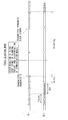
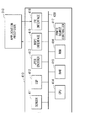
- Fig. 1 is a block diagram illustrating an outline of a communication system that transmits a data signal and a clock signal.
- Fig. 2 is a block diagram illustrating a configuration example of a communication system according to a comparative example that implements the communication system illustrated in Fig. 1.
- Fig. 3 is a circuit diagram illustrating a specific circuit configuration example of the communication system illustrated in Fig. 2.
- Fig. 4 is an explanatory diagram illustrating an example of respective signal waveforms to be transmitted on a clock lane and a data lane in the communication system illustrated in Fig.
- Fig. 5 is a block diagram illustrating an outline of a communication system according to a first embodiment of the present disclosure.
- Fig. 6 is a circuit diagram illustrating a specific circuit configuration example of the communication system according to the first embodiment.
- Fig. 7 is an explanatory diagram illustrating an example of a communication mode (a blanking mode) in a blanking period.
- Fig. 8 is an explanatory diagram illustrating an example of a frame structure of image data.
- Fig. 9 is an explanatory diagram illustrating a first example of respective signal waveforms to be transmitted on a clock lane and a data lane in the communication system according to the first embodiment.
- Fig. 5 is a block diagram illustrating an outline of a communication system according to a first embodiment of the present disclosure.
- Fig. 6 is a circuit diagram illustrating a specific circuit configuration example of the communication system according to the first embodiment.
- Fig. 7 is an explanatory diagram illustrating an example of a communication mode (a blanking mode) in
- FIG. 10 is an explanatory diagram illustrating a second example of respective waveforms to be transmitted on the clock lane and the data lane in the communication system according to the first embodiment.
- Fig. 11 is an explanatory diagram of a differential signal value.
- Fig. 12 is a block diagram illustrating an outline of a communication system according to a second embodiment.
- Fig. 13 is a block diagram illustrating a specific application example of the communication system according to the second embodiment.
- Fig. 14 is a flow chart illustrating an example of a data transmission process in the application example illustrated in Fig. 13.
- Fig. 15 is an explanatory diagram illustrating an example of data signal communication modes (data transmission modes).
- FIG. 16 is an explanatory diagram illustrating a first example of respective waveforms to be transmitted on a clock lane and a data lane in a communication system according to a third embodiment.
- Fig. 17 is an explanatory diagram illustrating an example of a method of discriminating communication modes in the first example illustrated in Fig. 16.
- Fig. 18 is an explanatory diagram illustrating a second example of respective waveforms to be transmitted on the clock lane and the data lane in the communication system according to the third embodiment.
- Fig. 19 is an explanatory diagram illustrating an example of a method of discriminating communication modes in the second example illustrated in Fig. 18.
- Fig. 17 is an explanatory diagram illustrating an example of a method of discriminating communication modes in the first example illustrated in Fig. 16.
- Fig. 18 is an explanatory diagram illustrating a second example of respective waveforms to be transmitted on the clock lane and the data lane in the communication system according to the third embodiment.
- Fig. 19 is an explan
- FIG. 20 is an explanatory diagram illustrating a third example of respective waveforms to be transmitted on the clock lane and the data lane in the communication system according to the third embodiment.
- Fig. 21 is an explanatory diagram illustrating an example of a method of discriminating communication modes in the third example illustrated in Fig. 20.
- Fig. 22 is a perspective view of an example of an appearance configuration of a smartphone to which any of the communication systems according to the respective embodiments is applied.
- Fig. 23 is a block diagram illustrating a configuration example of an application processor to which any of the communication systems according to the respective embodiments is applied.
- Fig. 24 is a block diagram illustrating a configuration example of an image sensor to which any of the communication systems according to the respective embodiments is applied.
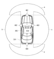
- FIG. 25 is an explanatory diagram illustrating an installation example of a vehicle-mounted camera to which any of the communication systems according to the respective embodiments is applied.
- Fig. 26 is a block diagram illustrating a configuration example of the vehicle-mounted camera to which any of the communication systems according to the respective embodiments is applied.
- HS differential signal is used for substantial data signal transmission.
- LP low power
- the HS differential signal and the LP signal are transmitted on a common transmission path.
- one transmission path (clock lane) where the clock signal is transmitted and one or more transmission paths (data lanes) where the data signal is transmitted may be provided.
- a signal transmission period on each of the clock lane and the data lane includes a period in which transmission using the HS differential signal is performed and a period in which transmission using the LP signal is performed.
- the HS differential signal and the LP signal are transmitted on the common transmission path.
- the LP signal is not a differential signal but a single-ended signal, and is different in voltage value necessary for signal transmission from the HS differential signal.
- a circuit for transmission and reception of the HS differential signal and a circuit for transmission and reception of the LP signal are necessary independently.
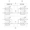
- Fig. 1 illustrates an outline of a communication system supporting a communication interface by, for example, the C-PHY specification or the D-PHY specification.
- the communication system illustrated in Fig. 1 includes a transmitter TX and a receiver RX.
- the communication system includes a clock lane CL and a data lane DL that are provided across the transmitter TX and the receiver RX.
- the clock lane CL allows a clock signal to be transmitted thereon.
- the data lane DL allows, for example, a data signal such as image data to be transmitted thereon.
- Fig. 1 illustrates an example in which four data lanes LD1, DL2, DL3, and DL4 are provided as the data lanes DL; however, the number of data lanes is not limited thereto, and only one data lane DL1 may be provided.
- the transmitter TX includes a transmission digital circuit TX-DIGITAL and a transmission analog circuit TX-ANALOG.
- a 16-bit or 8-bit parallel signal may be transmitted between the transmission digital circuit TX-DIGITAL and the transmission analog circuit TX-ANALOG.
- the receiver RX includes a reception digital circuit RX-DIGITAL and a reception analog circuit RX-ANALOG.
- a 16-bit or 8-bit parallel signal may be transmitted between the reception analog circuit RX-ANALOG and the reception digital circuit RX-DIGITAL on each of the data lanes DL1, DL2, DL3, and DL4.
- a 2-bit serial signal may be transmitted between the reception analog circuit RX-ANALOG and the reception digital circuit RX-DIGITAL on the clock lane CL.
- the transmission analog circuit TX-ANALOG and the reception analog circuit RX-ANALOG are coupled to each other by a clock signal line 30 on the clock lane CL.
- the clock signal line 30 allows a differential clock signal to be transmitted therethrough.
- the transmission analog circuit TX-ANALOG and the reception analog circuit RX-ANALOG are coupled to each other by data signal lines 31, 32, 33, and 34 on the data lanes DL1, DL2, DL3, and DL4, respectively.
- Each of the data signal lines 31, 32, 33, and 34A allows a differential data signal to be transmitted therethrough.
- Each of the clock signal line 30 and the data signal lines 31, 32, 33, and 34 includes a pair of a positive signal line Dp and a negative signal line Dn through which a differential signal is transmitted.
- a 2-bit serial signal may be transmitted through each of the clock signal line 30 and the data signal lines 31, 32, 33, and 34.
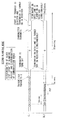
- Fig. 2 illustrates a configuration example of a communication system according to a comparative example that implements the communication system illustrated in Fig. 1. It is to be noted that Fig. 2 illustrates only one data lane DL1 as the data lane DL in Fig. 1; however, the other data lanes DL2, DL3, and DL4 may have a configuration substantially similar to that of the data lane DL1.
- the communication system according to this comparative example includes a transmitter 101 and a receiver 102.
- the transmitter 101 and the receiver 102 respectively correspond to the transmitter TX and the receiver RX in Fig. 1.
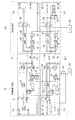
- the transmitter 101 On the clock lane CL, the transmitter 101 includes a CL-HS circuit 111 that processes the HS differential signal and a CL-LP circuit 112 that processes the LP signal. On the data lane DL1, the transmitter 101 includes a DL-HS circuit 113 that processes the HS differential signal and a DL-LP circuit 114 that processes the LP signal.
- Fig. 3 illustrates a specific circuit configuration example of the communication system according to the comparative example illustrated in Fig. 2.
- Fig. 4 illustrates an example of respective signal waveforms to be transmitted on the clock lane CL and the data lane DL1 in the communication system according to the comparative example illustrated in Fig. 2.
- a status of a signal to be outputted from the transmitter 101 to the data signal line 31 on the data lane CL has a high speed state (HSP) period and a low power state (LPS) period.
- HSP high speed state
- LPS low power state
- the signal is in a state of being transmitted in the form of the HS differential signal.
- LPS low power state
- a substantial data signal is outputted in the form of the HS differential signal in the HPS period.
- a substantial data signal portion is represented by "HST”.
- the HPS period may include, for example, a TRAIL period T HS-TRAIL and a SYNC (synchronization) period T HS-SYNC .
- a blanking period not including the substantial data signal portion is included in the LPS period.
- the substantial data signal may be outputted in a byte unit, for example.
- the communication system includes a crystal oscillator (XTAL) 82, a PLL circuit 81, and a crystal oscillator (XTAL) 83, as illustrated in Fig. 3.
- the crystal oscillator (XTAL) 82 and the PPL circuit 81 each supply the clock signal to respective circuit sections in the transmitter 101.
- the crystal oscillator (XTAL) 83 supplies the clock signal to respective circuit sections in the receiver 102.
- the CL-HS circuit 111 includes an HS state machine (HS FSM) 51, a selector 52, a parallel-serial (PS) conversion circuit 53, a clock frequency divider (DIV) 54, and an HS driver (HS DRV) 55.
- the selector 52 selectively outputs a Toggle signal, a signal with a value of 0 (ALL0), and a signal with a value of 1 (ALL1).
- the Toggle signal may be an 8-bit clock signal (1010_1010), for example.
- the CL-LP circuit 112 includes an LP state machine (LP FSM) 41, an LP encoder (LP ENC) 42, and an LP driver (LP DRV) 43.
- LP FSM LP state machine
- LP ENC LP encoder
- LP DRV LP driver
- the DL-LP circuit 114 includes an LP state machine (LP FSM) 61, an LP encoder (LP ENC) 62, and an LP driver (LP DRV) 63.
- LP FSM LP state machine
- LP ENC LP encoder
- LP DRV LP driver
- the LP driver 43, the HS driver 55, the LP driver 63, and the HS driver 74 in the transmitter 101 correspond to the transmission analog circuit TX-ANALOG in Fig. 1.
- the CL-HS circuit 121 includes a termination circuit (TERM) 56 serving as a clock signal termination circuit, an HS receiver (HS RCV) 57, and a clock frequency divider (DIV) 58.
- the termination circuit 56 includes a terminator.
- the CL-LP circuit 122 includes an LP receiver (LP RCV) 44, an LP decoder (LP DEC) 45, and an LP state machine (LP FSM) 46.
- the LP state machine 46 outputs a status signal of the clock lane CL.
- the DL-HS circuit 123 includes a termination circuit (TERM) 75 serving as a data signal termination circuit, an HS receiver (HS RCV) 76, a clock frequency divider (DIV) 77, and a word alignment correction circuit (ALN) 78.
- the termination circuit 75 includes a terminator.
- the word alignment correction circuit (ALN) 78 outputs a reception synchronization signal RxSyncHS, a reception valid signal RxValidHS, and reception data RxDataHS.
- the DL-LP circuit 124 includes an LP receiver (LP RCV) 64, an LP decoder (LP DEC) 65, and an LP state machine (LP FSM) 66.
- the LP state machine 66 outputs a reception active signal RxActiveHS.
- the communication system according to the comparative example illustrated in Figs. 2 to 4 uses a communication mode in which an LP signal having a voltage of about 1.3 V is outputted in the blanking periods of the clock signal and the data signal.
- an LP signal having a voltage of about 1.3 V is outputted in the blanking periods of the clock signal and the data signal.
- all signals to be outputted from the transmitter 1 to the clock signal line 30 including the blanking period are HS differential signals only.
- all signals to be outputted from the transmitter 1 to the data signal line 31 including the blanking period are HS differential signals only.
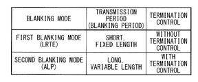
- the communication system according to the present embodiment has a plurality of communication modes (blanking modes) in the blanking period.
- Fig. 7 illustrates an example of blanking modes in the present embodiment.
- examples of the blanking modes may include a first blanking mode in which a transmission period is relatively short and a second blanking mode in which a transmission period is relatively long.
- the first blanking mode is a communication (Latency Reduction Transport Efficiency: LRTE) mode in which a blanking interval is minimized.
- LRTE Location Reduction Transport Efficiency
- the transmission period has a fixed length.
- the LRTE mode is a mode in which termination control is not performed (on-off switching of a terminator is not performed).
- the second blanking mode is a communication (Alternate LP: ALP) mode suitable for a long blanking period.
- ALP Alternate LP
- the transmission period has a variable length.
- the ALP mode is a mode in which it is possible to perform termination control (on-off switching of the terminator is possible).
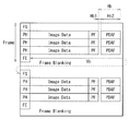
- Fig. 8 illustrates an example of a frame structure of image data to be transmitted in the communication system according to the present embodiment.
- Fig. 8 illustrates a frame structure of two frames of image data.
- a header of the frame is referred to as "FS (frame start)”
- a footer of the frame is referred to as "FE (frame end)”.
- An interval between the two frames is a frame blanking period (vertical blanking period) Vb.
- a header of one horizontal period is referred to as "packet header”
- PF packet footer
- a data signal may be inserted into a horizontal blanking period Hb.
- the data signal may include a phase difference detection data PDAF (Phase Detection Auto-Focus) used for phase-difference auto-focusing.
- PDAF Phase Detection Auto-Focus
- a period Hb1 excluding a period Hb2 into which the data signal such as PDAF (Phase Detection Auto-Focus) is inserted is a substantial horizontal blanking period.
- the horizontal blanking period Hb1 is extremely short. Accordingly, in the communication system according to the present embodiment, the first blanking mode (the LRTE mode) is suitable as the blanking mode for communication in the horizontal blanking period Hb1. Moreover, the second blanking mode (the ALP mode) is suitable for communication in the vertical blanking period Vb.
- the present embodiment makes it possible to discriminate the plurality of communication mode without using the counter.
- the blanking controller 20 may control, depending on the communication modes, a signal value of a data blanking signal and a signal value of a clock blanking signal to, for example, values that enable discrimination of the communication modes as illustrated in Figs. 9 and 10 to be described later.
- a clock state discrimination circuit 59 (Fig. 6) to be described later may discriminate the communication modes with reference to, for example, values illustrated in Figs. 9 and 10 to be described later.
- Fig. 9 illustrates a first example of respective signal waveforms to be transmitted on the clock lane CL and the data lane DL1 in the communication system according to the present embodiment.
- Fig. 9 illustrates an example in which the communication mode in the blanking period is the first blanking mode (the LRTE mode).
- a substantial data signal portion in Figs. 9 and 10 is referred to as "HST".
- Periods before and after a substantial data signal may include a SYNC (synchronization) period T HS-SYNC and a TRAIL period T HS-TRAIL .
- the communication system may include the crystal oscillator (XTAL) 82, the PLL circuit 81, the crystal oscillator (XTAL) 83, and a PPL circuit 84.
- the crystal oscillator (XTAL) 82 and the PLL circuit 81 each supply the clock signal to respective circuit portions in the transmitter 1.
- the crystal oscillator (XTAL) 83 and the PLL circuit 84 each supply the clock signal to respective circuit portions in the receiver 2.
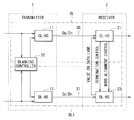
- the transmitter 1 On the clock lane CL, the transmitter 1 may include a CL-HS circuit 11 that processes the HS differential signal. On the data lane DL1, the transmitter 1 may include a DL-HS circuit 13 that processes the HS differential signal.
- the CL-HS circuit 11 may be a differential clock signal transmitter circuit that outputs the clock signal and the HS differential signal as a clock blanking signal to the clock signal line 30.
- the DL-HS circuit 13 may be a differential data signal transmitter circuit that outputs the data signal and the HS differential signal as a data blanking signal to the data signal line 31.
- the transmitter 1 may not include circuits corresponding to the CL-LP circuit 112 and the DL-LP circuit 114 that each process the LP signal in the foregoing comparative example.
- the CL-HS circuit 11 may include a circuit substantially similar to the CL-HS circuit 111 in Fig. 3, as illustrated in Fig. 6. More specifically, the CL-HS circuit 11 may include the HS state machine (HS FSM) 51, the selector 52, the parallel-serial (PS) conversion circuit 53, the clock frequency divider (DIV) 54, and the HS driver (HS DRV) 55.
- the selector 52 may selectively output the Toggle signal, the signal with a value of 0 (ALL0), and the signal with a value of 1 (ALL1).
- the Toggle signal may be an 8-bit clock signal (1010_1010), for example.
- the clock lane control signal and the data transmission request signal TxRequestHS may be inputted into the HS state machine 51.
- the DL-HS circuit 13 may include circuits substantially similar to the DL-HS circuit 113 in Fig. 3, as illustrated in Fig. 6. More specifically, the DL-HS circuit 13 may include the HS state machine (HS FSM) 71, the selector 72, the parallel-serial (PS) conversion circuit 73, and the HS driver (HS DRV) 74.
- the HS state machine 71 may output the data transmission ready signal TxReadyHS.
- the selector 72 may selectively output the transmission data TxDataHS, the synchronization code signal SYNC, the signal with a value of 0 (ALL0), and the signal with a value of 1 (ALL1).
- the blanking controller 20 may include the HS state machine 51 and the HS state machine 71, as illustrated in Fig. 6.
- the blanking controller 20 may control the DL-HS circuit 13 so as to output, for example, a data blanking signal with a value of 1, in place of the data signal from the DL-HS circuit 13, from the DL-HS circuit 13 to the data signal line 31 in synchronization with start time of a blanking period of the data signal.
- the blanking controller 20 may control the CL-HS circuit 11 so as to output, for example, a differential blanking signal, in place of the clock signal, from the CL-HS circuit 11 to the clock signal line 30 in synchronization with the start time of the blanking period of the data signal throughout a predetermined period or longer.
- a clock blanking signal with a value of 0 may continue.
- the predetermined period herein is a period that is longer than a clock cycle of the clock signal.
- the clock blanking signal is a signal continuously having a signal value of 0 throughout a period longer than the clock cycle of the clock signal, which makes it possible to detect a signal change in the clock state discrimination circuit 59 of the receiver 2, thereby detecting that the blanking period has started.
- the blanking controller 20 may control the CL-HS circuit 11 so as to output the clock signal, in place of the clock blanking signal, from the CL-HS circuit 11 to the clock signal line 30 in synchronization with end time of the blanking period of the data signal throughout a predetermined period or longer. Outputting the clock signal, in place of the clock blanking signal, throughout the predetermined period or longer makes it possible to detect a signal change in the clock state discrimination circuit 59 of the receiver 2, thereby detecting that the blanking period has ended and transfer of the data signal is to start.
- the blanking controller 20 may control the DL-HS circuit 13 so as to output a data blanking signal with a value of 0, in place of the data signal, from the DL-HS circuit 13 to the data signal line 31 in synchronization with the start time of the blanking period of the data signal.
- the blanking controller 20 may control the CL-HS circuit 11 so as to output, for example, a differential blanking signal, in place of the clock signal, from the CL-HS circuit 11 to the clock signal line 30 in synchronization with the start time of the blanking period of the data signal throughout a predetermined period or longer.
- a clock blanking signal with a value of 0 may continue.
- the predetermined period herein is a period longer than the clock cycle of the clock signal.
- the clock blanking signal is a signal continuously having a signal value of 0 throughout a period longer than the clock cycle of the clock signal, which makes it possible to detect a signal change in the clock state discrimination circuit 59 of the receiver 2, thereby detecting that the blanking period has started.
- the blanking controller 20 may control the CL-HS circuit 11 so as to output, for example, a clock blanking signal with a value of 1, in place of the clock blanking signal with a value of 0, from the CL-HS circuit 11 to the clock signal line 30 in synchronization with the end time of the blanking period of the data signal throughout a predetermined period or longer.
- Outputting the clock blanking signal with a value of 1, in place of the clock blanking signal with a value of 0, throughout the predetermined period or longer makes it possible to detect a signal change in the clock state discrimination circuit 59 of the receiver 2, thereby detecting that the blanking period has ended and transfer of the data signal is to start.
- the value of the data blanking signal at the start of the blanking period of the data signal is different between the first blanking mode and the second blanking mode, which makes it possible to discriminate the communication modes in the clock state discrimination circuit 59 of the receiver 2.
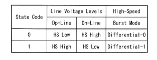
- Fig. 11 illustrates an example of a value of a differential signal.
- the clock blanking signal with a value of 0 and the data blanking signal with a value of 0 may be differential signals with a differential of 0 (Differential-0).
- the clock blanking signal with a value of 1 and the data blanking signal with a value of 1 may be differential signals with a differential of 1 (Differential-1).
- the differential signal with a value of 0 may be a differential signal in which a voltage level of a positive signal line Dp and a voltage level of a negative signal line Dn on a transmission line of the differential signal are low and high, respectively.
- the differential signal with a value of 1 may be a differential signal in which the voltage level of the positive signal line Dp and the voltage level of the negative signal line Dn on the transmission line of the differential signal are high and low, respectively.
- the receiver 2 On the clock lane CL, the receiver 2 may include a CL-HS circuit 21 that processes the HS differential signal. On the data lane DL1, the receiver 2 may include a DL-HS circuit 23 that processes the HS differential signal.
- the DL-HS circuit 23 may be a differential data signal receiver circuit that receives the data signal and the HS differential signal as a data blanking signal through the data signal line 31.
- the CL-HS circuit 21 may be a differential clock signal receiver circuit that receives the clock signal and the HS differential signal as a clock blanking signal through the clock signal line 30.
- the receiver 2 may not include circuits corresponding to the CL-LP circuit 122 and the DL-LP circuit 124 that each process the LP signal in the foregoing comparative example.
- the DL-HS circuit 23 may include a circuit substantially similar to the DL-HS circuit 123 in Fig. 3, as illustrated in Fig. 6. More specifically, the DL-HS circuit 23 may include the termination circuit (TERM) 75 serving as a data signal termination circuit coupled to the data signal line 31, the HS receiver (HS RCV) 76, the clock frequency divider (DIV) 77, and the word alignment correction circuit (ALN) 78.
- the termination circuit 75 may include a terminator.
- the word alignment correction circuit (ALN) 78 may output the reception synchronization signal RxSyncHS, the reception valid signal RxValidHS, and the reception data RxDataHS.
- the CL-HS circuit 21 may include a circuit substantially similar to the CL-HS circuit 121 in Fig. 3, as illustrated in Fig. 6. More specifically, the CL-HS circuit 21 may include the termination circuit (TERM) 56 serving as a clock signal termination circuit coupled to the clock signal line 30, the HS receiver (HS RCV) 57, and the clock frequency divider (DIV) 58.
- the termination circuit 56 may include a terminator.
- the CL-HS circuit 21 may further include the clock (CL) state discrimination circuit 59.
- the clock signal and the clock blanking signal from the CL-HS circuit 11 of the transmitter 1 may be inputted to the clock state discrimination circuit 59 through the HS receiver 57.
- the data blanking signal from the DL-HS circuit 13 of the transmitter 1 may be inputted to the clock state discrimination circuit 59 through the HS receiver 76.
- the clock state discrimination circuit 59 may discriminate the blanking modes with reference to, for example, the value of the data blanking signal at the start of the blanking period of the data signal. For example, in a case in which the value of the data blanking signal is 1 as with the example in Fig. 9, the clock state discrimination circuit 59 may discriminate that the blanking mode is the first blanking mode. Moreover, for example, in a case in which the value of the data blanking signal is 0 as with the example in Fig. 10, the clock state discrimination circuit 59 may discriminate that the blanking mode is the second blanking mode.
- the receiver 2 may perform a termination control process.
- the clock state discrimination circuit 59 may function as a termination control circuit.
- the clock state discrimination circuit 59 may perform control to cause the terminator of the data signal termination circuit (the termination circuit 75) and the terminator of the clock signal termination circuit (the termination circuit 56) to be turned off on the basis of, for example, the clock blanking signal with a value of 0.
- the clock state discrimination circuit 59 may perform control to cause the terminator of the termination circuit 75 and the terminator of the termination circuit 56 to be turned on, on the basis of the clock blanking signal with a value of 1 that is outputted in synchronization with the end time of the blanking period of the data signal.
- the clock state discrimination circuit 59 may have a function of outputting the reception active signal RxActiveHS and performing word alignment control on the word alignment correction circuit 78.
- the clock state discrimination circuit 59 properly detects that the blanking period is ended and transfer of the data signal starts, which makes it possible for the word alignment correction circuit 78 to perform word alignment control properly.
- the differential blanking signal in which the predetermined value continues throughout the predetermined period or longer is outputted as the clock blanking signal, in place of the clock signal, to the clock signal line 30 in synchronization with the start time of the blanking period of the data signal, which makes it possible to reduce power consumption during data transmission.
- the circuit that processes the LP signal is unnecessary, which makes it possible to reduce a circuit size.
- the signal value of the data blanking signal is controlled to a value that enables discrimination of the blanking modes in the transmitter 1, and the blanking modes are discriminated on the basis of the signal value of the data blanking signal in the receiver 2.
- the communication system according to the present embodiment may include a switching circuit that makes it possible to perform communication using the LP signal.
- the switching circuit makes it possible to perform switching between a mode in which communication using the HS differential signal without using the LP signal is performed and a mode in which communication using both the LP signal and the HS differential signal is performed.
- the transmitter 1B may include the CL-HS circuit 11 that processes the HS differential signal, a CL-LP circuit 12 that processes the LP signal, a selector switch 15, and a selector 17 on the clock lane CL.
- the CL-LP circuit 12 may be a first single-ended signal transmitter circuit that outputs a first signal-ended signal as the LP signal.
- the CL-LP circuit 12 may have a function substantially similar to that of the CL-LP circuit 112 in Fig. 2.
- the selector switch 15 may be a first transmission switching circuit that switches a signal output path to cause one of the CL-HS circuit 11 and the CL-LP circuit 12 to output a signal to the clock signal line 30.
- the selector 17 may be a circuit that causes a control signal from the blanking controller 20 to be inputted to the CL-HS circuit 11 in a mode in which communication using only the HS differential signal without using the LP signal is performed, and prevents the control signal from the blanking controller 20 from being inputted to the CL-HS circuit 11 in a mode in which communication using both the LP signal and the HS differential signal is performed.
- the transmitter 1B may include the DL-HS circuit 13 that processes the HS differential signal, the DL-LP circuit 14 that processes the LP signal, a selector switch 16, and a selector 18 on the data lane DL1.
- the DL-LP circuit 14 may be a second single-ended signal transmitter circuit that outputs a second single-ended signal as the LP signal.
- the DL-LP circuit 14 may have a function substantially similar to that of the DL-LP circuit 114 in Fig. 2.
- the selector switch 16 may be a second transmission switching circuit that switches a signal output path to cause one of the DL-HS circuit 13 and the DL-LP circuit 14 to output a signal to the data signal line 31.
- the selector 18 may be a circuit that causes a control signal from the blanking controller 20 to be inputted to the DL-HS circuit 13 in the mode in which communication using only the HS differential signal without using the LP signal is performed, and prevents the control signal from the blanking controller 20 from being inputted to the DL-HS circuit 13 in the mode in which communication using both the LP signal and the HS differential signal is performed.
- the receiver 2B may include the CL-HS circuit 21 that processes the HS differential signal, a CL-LP circuit 22 that processes the LP signal, a selector 25, a selector 27, and a selector 28.
- the CL-LP circuit 22 may be a first single-ended signal receiver circuit that receives the first single-ended signal as the LP signal through the clock signal line 30.
- the CL-LP circuit 22 may have a function substantially similar to that of the CL-LP circuit 122 in Fig. 2.
- the selector 25 may be a first reception switching circuit that performs switching whether to receive the first single-ended signal as the LP signal.
- the selector 25 may be a circuit that prevents a signal received through the clock signal line 30 from being inputted to the CL-LP circuit 22 in the mode in which communication using only the HS differential signal without using the LP signal is performed, and causes the signal received through the clock signal line 30 to be inputted to the CL-LP circuit 22 in the mode in which communication using both the LP signal and the HS differential signal is performed.
- the selector 27 may be a circuit that inputs a termination control signal from the CL-HS circuit 21 to the DL-HS circuit 23 in the mode in which communication using only the HS differential signal without using the LP signal is performed, and prevents the termination control signal from the CL-HS circuit 21 from being inputted to the DL-HS circuit 23 in the mode in which communication using both the LP signal and the HS differential signal is performed.
- the selector 28 may be a circuit that causes a word alignment control signal from the CL-HS circuit 21 to be inputted to the DL-HS circuit 23 in the mode in which communication using only the HS differential signal without using the LP signal is performed, and prevents the word alignment control signal from the CL-HS circuit 21 from being inputted to the DL-HS circuit 23 in the mode in which communication using both the LP signal and the HS differential signal is performed.
- the receiver 2B may include the DL-HS circuit 23 that processes the HS differential signal, a DL-LP circuit 24 that processes the LP signal, and a selector 26 on the data lane DL1.
- the DL-LP circuit 24 may be a second single-ended signal receiver circuit that receives the second single-ended signal as an LP signal through the data signal line 31.
- the selector 26 may be a second reception switching circuit that performs whether to receive the second single-ended signal as the LP signal.
- the selector 26 may be a circuit that prevents a signal received through the data signal line 31 from being inputted to the DL-LP circuit 24 in the mode in which communication using only the HS differential signal without using the LP signal is performed, and causes the signal received through the data signal line 31 to be inputted to the DL-LP circuit 24 in the mode in which communication using both the LP signal and the HS differential signal is performed.
- Fig. 13 illustrates a specific application example of the communication system according to the present embodiment.
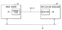
- the communication system according to the present embodiment is applicable to data transmission from an image sensor IS to an application processor AP, as illustrated in Fig. 13.
- the transmitter 1B may be provided in the image sensor IS.
- the receiver 2B may be provided in the application processor AP.
- the image sensor IS and the application processor AP may be coupled to each other through the clock signal line 30 and the data signal line 31. Signals may be transmitted through the clock signal line 30 and the data signal line 31 in one direction.
- the image sensor IS and the application processor AP may be coupled to each other through a bidirectional control bus 35.
- the control bus 35 may use an I 2 C (Inter-Integrated Circuit) interface or an I 3 C interface that is an extension of the I 2 C interface.
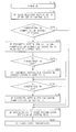
- Fig. 14 illustrates an example of a data transmission process in a device including the image sensor IS and the application processor AP illustrated in Fig. 13.
- the device including the image sensor IS and the application processor AP may be powered on (step S101).
- the application processor AP may read a register setting of the image sensor IS with use of the control bus 35 (step S102).
- the application processor AP may determine whether the image sensor IS corresponds to communication without the LP signal (step S103). In other words, the application processor AP may determine whether the image sensor IS corresponds to the mode in which communication using only the HS differential signal without using the LP signal is performed or the mode in which communication using both the LP signal and the HS differential signal is performed.
- the application processor AP may determine that the image sensor IS is in the mode in which communication using both the LP signal and the HS differential signal is performed, and may output a transmission start command signal to the image sensor IS with use of the control bus 35 (step S109).
- the image sensor IS may start transmission of the data signal in response to the transmission start command signal (step S110).
- the application processor AP may transmit a setting for validating communication without the LP signal to the image sensor IS (step S104).
- the application processor AP may determine whether the image sensor IS corresponds to communication by the first blanking mode (the LRTE mode) with reference to the register setting of the image sensor IS (step S105). In a case in which the application processor AP determines that the image sensor IS does not correspond to communication by the first blanking mode (step S105; N), the flow of the data transmission process proceeds to a process in step S107 to be described later. In a case in which the application processor AP determines that the image sensor IS corresponds to communication by the first blanking mode (step S105; Y), the application processor AP may transmit a setting for validating communication by the first blanking mode to the image sensor IS with use of the control bus 35 (step S106).
- the application processor AP may determine whether the image sensor IS corresponds to communication by the second blanking mode (the ALP mode) with reference to the register setting of the image sensor IS (step S107). In a case in which the application processor AP determines that the image sensor IS does not correspond to communication by the second blanking mode (step S107; N), the application processor AP may output a transmission start command signal to the image sensor IS with use of the control bus 35 (step S109). Next, the image sensor IS may start transmission of the data signal in response to the transmission start command signal (step S110).
- the application processor AP may transmit a setting for validating communication by the second blanking mode to the image sensor IS with use of the control bus 35 (step S108).
- the application processor AP may output the transmission start command signal to the image sensor IS with use of the control bus 35 (step S109).
- the image sensor IS may start transmission of the data signal in response to the transmission start command signal (step S110).
- Fig. 15 illustrates an example of data transmission modes to be discriminated in the present embodiment.
- the data transmission modes for example, a first data transmission mode (a high-speed transmission mode) in which transmission speed is relatively high and a second data transmission mode (a low-speed transmission mode) in which the transmission speed is relatively low may be discriminated.
- the high-speed transmission mode and the low-speed transmission mode may be both modes in which a differential signal is transmitted, and may have different transmission speed, for example, by changing a voltage amplitude.
- a basic configuration of the communication system in the present embodiment may be substantially similar to the configuration in Figs. 5 and 6.
- the blanking controller 20 may control, depending on the communication modes, the signal value of the data blanking signal and the signal value of the clock blanking signal to, for example, values that enable discrimination of the communication modes as illustrated in Figs. 17, 19, and 21 to be described later.
- the clock state discrimination circuit 59 may discriminate the communication modes with reference to, for example, values illustrated in Figs. 17, 19 and 21 to be described later.
- Fig. 16 illustrates a first example of respective signal waveforms to be transmitted on the clock lane CL and the data lane DL1 in the communication system according to the present embodiment.
- Fig. 16 illustrates an example in which the communication mode in the blanking period is the first blanking mode (the LRTE mode), as with the example in Fig. 9.
- Fig. 17 illustrates an example of a method of discriminating the communication modes of the data signal in a case in which the communication mode in the blanking period is the first blanking mode.
- the blanking controller 20 may control the DL-HS circuit 13 so as to output, for example, a data blanking signal with a value D nt 0, in place of the data signal, from the DL-HS circuit 13 to the data signal line 31 in synchronization with the start time of the blanking period of the data signal.
- the blanking controller 20 may control the CL-HS circuit 11 so as to output, in place of the clock signal, a differential blanking signal from the CL-HS circuit 11 to the clock signal line 30 in synchronization with the start time of the blanking period of the data signal throughout a predetermined period or longer.
- a clock blanking signal with a value C nt 0 may continue.
- the predetermined period herein is a period that is longer than the clock cycle of the clock signal.
- the clock blanking signal is a signal continuously having the signal value C nt 0 throughout a period longer than the clock cycle of the clock signal, which makes it possible to detect a signal change in the clock state discrimination circuit 59 of the receiver 2, thereby detecting that the blanking period has started.
- the blanking controller 20 may control the CL-HS circuit 11 so as to output the clock signal, in place of the clock blanking signal, from the CL-HS circuit 11 to the clock signal line 30 in synchronization with the end time of the blanking period of the data signal throughout a predetermined period or longer. Outputting the clock signal, in place of the clock blanking signal, throughout the predetermined period or longer makes it possible to detect a signal change in the clock state discrimination circuit 59 of the receiver 2, thereby detecting that the blanking period has ended and transfer of the data signal is to start.
- the clock state discrimination circuit 59 may discriminate the communication modes with reference to the values as illustrated in Fig. 17, for example.
- Fig. 18 illustrates a second example of respective signal waveforms to be transmitted on the clock lane CL and the data lane DL1 in the communication system according to the present embodiment.
- Fig. 18 illustrates an example in which the communication mode in the blanking period is the second blanking mode (the ALP mode) as with the example in Fig. 10.
- Fig. 19 illustrates an example of a method of discriminating the communication modes of the data signal in a case in which the communication mode in the blanking period is the second blanking mode.
- the blanking controller 20 may control the DL-HS circuit 13 so as to output, for example, a data blanking signal with a value D0, in place of the data signal, from the DL-HS circuit 13 to the data signal line 31 in synchronization with the start time of the blanking period of the data signal. Moreover, the blanking controller 20 may control the DL-HS circuit 13 so as to output, in place of the data blanking signal with the value D0, a data blanking signal with a value D1 from the DL-HS circuit 13 to the data signal line 31 in synchronization with the end time of the blanking period.
- the blanking controller 20 may control the CL-HS circuit 11 so as to output, in place of the clock signal, a differential blanking signal from the CL-HS circuit 11 to the clock signal line 30 in synchronization with the start time of the blanking period of the data signal throughout a predetermined period or longer.
- a clock blanking signal with a value C0 may continue.
- the predetermined period herein is a period that is longer than the clock cycle of the clock signal.
- the clock blanking signal is a signal continuously having the signal value C0 throughout a period longer than the clock cycle of the clock signal, which makes it possible to detect a signal change in the clock state discrimination circuit 59 of the receiver 2, thereby detecting that the blanking period has started.
- the blanking controller 20 may control the CL-HS circuit 11 so as to output the clock blanking signal with a value C1, in place of the clock blanking signal with the value C0, from the CL-HS circuit 11 to the clock signal line 30 in synchronization with the end time of the blanking period of the data signal throughout a predetermined period or longer.
- Outputting the clock blanking signal with the value C1, in place of the clock blanking signal with the value C0, throughout the predetermined period or longer makes it possible to detect a signal change in the clock state discrimination circuit 59 of the receiver 2, thereby detecting that the blanking period has ended and transfer of the data signal is to start.
- the clock state discrimination circuit 59 may discriminate the communication modes with reference to the values as illustrated in Fig. 19, for example.
- Fig. 20 illustrates a third example of respective signal waveforms to be transmitted on the clock lane CL and the data lane DL1 in the communication system according to the present embodiment.
- Fig. 21 illustrates an example of a method of discriminating the communication modes in the third example illustrated in Fig. 20.
- Fig. 20 illustrates an example in which transition of the communication modes takes place in order of the high-speed transmission mode, the LRTE mode, the low-speed transmission mode, and the high-speed transmission mode.
- the clock state discrimination circuit 59 may discriminate the communication mode with reference to the value (C0, C1) on the clock lane CL and the value (D0, D1) on the data lane DL1 as illustrated in Fig. 21, for example. It is to be noted that Fig. 21 illustrates an example of an on-off state of the terminator during mode transition.
- First Application Example Fig. 22 illustrates an appearance of a smartphone 300 (a multifunctional mobile phone) to which any of the communication systems according to the foregoing respective embodiments is applied.
- Various devices are mounted in the smartphone 300. Any of the communication systems according to the foregoing respective embodiments is applied to a communication system that exchanges data between these devices.
- Fig. 23 illustrates a configuration example of an application processor 310 used in the smartphone 300.
- the application processor 310 may include a central processing unit (CPU) 311, a memory controller 312, a power source controller 313, an external interface 314, a graphics processing unit (GPU) 315, a media processor 316, a display controller 317, and a mobile industry processor interface (MIPI) interface 318.
- the CPU 311, the memory controller 312, the power source controller 313, the external interface 314, the GPU 315, the media processor 316, and the display controller 317 may be coupled to a system bus 319 to allow for data exchange through the system bus 319.
- the CPU 311 may be adapted to process various pieces of information handled in the smartphone 300 in accordance with a program.
- the memory controller 312 may be adapted to control the memory 501 used when the CPU 311 performs information processing.
- the power source controller 313 may be adapted to control a power source of the smartphone 300.
- the external interface 314 may be an interface for communication with external devices.
- the external interface 314 may be coupled to a wireless communication section 502 and an image sensor 410.
- the wireless communication section 502 may be adapted to carry out wireless communication with mobile phone base stations.
- the wireless communication section 502 may include, for example, a baseband section, a radio frequency (RF) front end section, and other components.
- the image sensor 410 may be adapted to acquire an image, and may include, for example, a CMOS sensor.
- the GPU 315 may be adapted to perform image processing.
- the media processor 316 may be adapted to process information such as voice, characters, and graphics.
- the display controller 317 may be adapted to control the display 504 through the MIPI interface 318.
- the MIPI interface 318 may be adapted to transmit an image signal to the display 504.
- an image signal for example, a YUV-format signal, an RGB-format signal, or any other format signal may be used.
- any of the communication systems according to the foregoing respective embodiments may be applied to a communication system between the MIPI interface 318 and the display 504.
- Fig. 24 illustrates a configuration example of the image sensor 410.
- the image sensor 410 may include a sensor 411, an image signal processor (ISP) 412, a joint photographic experts group (JPEG) encoder 413, a CPU 414, a random access memory (RAM) 415, a read only memory (ROM) 416, a power source controller 417, an inter-integrated circuit (I 2 C) interface 418, and an MIPI interface 419.
- ISP image signal processor
- JPEG joint photographic experts group
- RAM random access memory
- ROM read only memory
- I 2 C inter-integrated circuit
- the sensor 411 may be adapted to acquire an image, and may be configured of, for example, a CMOS sensor.
- the ISP 412 may be adapted to perform predetermined processing on the image acquired by the sensor 411.
- the JPEG encoder 413 may be adapted to encode the image processed by the ISP 412 to generate a JPEG-format image.
- the CPU 414 may be adapted to control respective blocks of the image sensor 410 in accordance with a program.
- the RAM 415 may be a memory used when the CPU 414 performs information processing.
- the ROM 416 may be adapted to store a program to be executed in the CPU 414.
- the power source controller 417 may be adapted to control a power source of the image sensor 410.
- the I 2 C interface 418 may be adapted to receive a control signal from the application processor 310.
- the image sensor 410 may be adapted to also receive a clock signal from the application processor 310, in addition to the control signal. More specifically, the image sensor 410 may be configured to be operable on the basis of clock signals of various frequencies.
- the MIPI interface 419 may be adapted to transmit an image signal to the application processor 310.
- the image signal for example, a YUV-format signal, an RGB-format signal, or any other format signal may be used.
- any of the communication systems according to the foregoing respective embodiments may be applied to a communication system between the MIPI interface 419 and the application processor 310.
- Fig. 25 and Fig. 26 each illustrate a configuration example of a vehicle-mounted camera as an application example to an imaging device.
- Fig. 25 illustrates an installation example of the vehicle-mounted camera
- Fig. 26 illustrates an internal configuration example of the vehicle-mounted camera.
- vehicle-mounted cameras 401, 402, 403, and 404 may be respectively mounted on the front, left, right, and rear of a vehicle 301, as illustrated in Fig. 25.
- the vehicle-mounted cameras 401 to 404 may be coupled to an electrical control unit (ECU) 302 through an in-vehicle network.
- ECU electrical control unit
- An image capturing angle of the vehicle-mounted camera 401 mounted on the front of the vehicle 301 may be within a range indicated by "a" in Fig. 25, for example.
- An image capturing angle of the vehicle-mounted camera 402 may be within a range indicated by "b” in Fig. 25, for example.
- An image capturing angle of the vehicle-mounted camera 403 may be within a range indicated by "c” in Fig. 25, for example.
- An image capturing angle of the vehicle-mounted camera 404 may be within a range indicated by "d” in Fig. 25, for example.
- Each of the vehicle-mounted cameras 401 to 404 may output a captured image to the ECU 302. This makes it possible to capture a 360-degree (omnidirectional) image on the front, right, left, and rear of the vehicle 301 in the ECU 302.
- each of the vehicle-mounted cameras 401 to 404 may include an image sensor 431, a digital signal processing (DSP) circuit 432, a selector 433, and a serializer-deserializer (SerDes) circuit 434, as illustrated in Fig. 26.
- DSP digital signal processing
- SerDes serializer-deserializer
- the DSP circuit 432 may be adapted to perform various kinds of image signal processing on an imaging signal outputted from the image sensor 431.
- the SerDes circuit 434 may be adapted to perform serial-parallel conversion of a signal, and may be configured of, for example, a vehicle-mounted interface chip such as DPD-Link III.
- the selector 433 may be adapted to select whether to output the imaging signal outputted from the image sensor 431 through the DSP circuit 432 or not through the DSP circuit 432.
- any of the communication systems according to the foregoing respective embodiments may be applied to, for example, a connection interface 441 between the image sensor 431 and the DSP circuit 432.
- any of the communication systems according to the foregoing respective embodiments may be applied to, for example, a connection interface 442 between the image sensor 431 and the selector 433.
- a reception device including: a data signal receiver circuit that receives a data signal through a data signal line, and receives a data blanking signal through the data signal line in a blanking period of the data signal; a clock signal receiver circuit that receives a clock signal and a clock blanking signal through a clock signal line, the clock blanking signal outputted in synchronization with the blanking period of the data signal; and a discrimination circuit that discriminates communication modes on a basis of one or both of a signal value of the data blanking signal and a signal value of the clock blanking signal.
- the discrimination circuit discriminates at least communication modes in the blanking period.
- the data signal receiver circuit is a differential data signal receiver circuit that receives the data signal, and a differential signal as the data blanking signal through the data signal line
- the clock signal receiver circuit is a differential clock signal receiver circuit that receives the clock signal, and a differential signal as the clock blanking signal through the clock signal line.
- a transmission device including: a data signal transmitter circuit that outputs a data signal to a data signal line, and outputs a data blanking signal through the data signal line in a blanking period of the data signal; a clock signal transmitter circuit that outputs a clock signal to a clock signal line, and outputs a clock blanking signal, in place of the clock signal, in synchronization with the blanking period of the data signal; and a blanking controller that controls one or both of a signal value of the data blanking signal and a signal value of the clock blanking signal to a value that enables discrimination of communication modes.
- the blanking controller controls the signal value to a value that enables discrimination of at least communication modes in the blanking period.
- the blanking controller controls the signal value to a value that enables discrimination of a first data transmission mode and a second data transmission mode as the communication modes of the data signal, the second data transmission mode in which transmission speed is lower than transmission speed in the first data transmission mode.
- the data signal transmitter circuit is a differential data signal transmitter circuit that outputs the data signal, and a differential signal as the data blanking signal through the data signal line
- the clock signal transmitter circuit is a differential clock signal transmitter circuit that outputs the clock signal, and a differential signal as the clock blanking signal through the clock signal line.
- a communication system including: a transmission device; and a reception device, the transmission device including: a data signal transmitter circuit that outputs a data signal to a data signal line, and outputs a data blanking signal through the data signal line in a blanking period of the data signal, a clock signal transmitter circuit that outputs a clock signal to a clock signal line, and outputs a clock blanking signal, in place of the clock signal, in synchronization with the blanking period of the data signal, and a blanking controller that controls one or both of a signal value of the data blanking signal and a signal value of the clock blanking signal to a value that enables discrimination of communication modes, and the reception device including: a data signal receiver circuit that receives the data signal and the data blanking signal through the data signal line, a clock signal receiver circuit that receives the clock signal and the clock blanking signal through the clock signal line, and a discrimination circuit that discriminates the communication modes on a basis of one or both of the signal value of the data blanking signal and the signal value of
- a signal reception method including: receiving a data signal through a data signal line, and receiving a data blanking signal through the data signal line in a blanking period of the data signal; receiving a clock signal and a clock blanking signal through a clock signal line, the clock blanking signal outputted in synchronization with the blanking period of the data signal; and discriminating communication modes on a basis of one or both of a signal value of the data blanking signal and a signal value of the clock blanking signal.
- a signal transmission method including: outputting a data signal to a data signal line, and outputting a data blanking signal through the data signal line in a blanking period of the data signal; outputting a clock signal to a clock signal line, and outputting a clock blanking signal, in place of the clock signal, in synchronization with the blanking period of the data signal; and controlling one or both of a signal value of the data blanking signal and a signal value of the clock blanking signal to a value that enables discrimination of communication modes.
- a communication method including: outputting a data signal to a data signal line, and outputting a data blanking signal through the data signal line in a blanking period of the data signal; outputting a clock signal to a clock signal line, and outputting a clock blanking signal, in place of the clock signal, in synchronization with the blanking period of the data signal; controlling one or both of a signal value of the data blanking signal and a signal value of the clock blanking signal to a value that enables discrimination of a communication mode; receiving the data signal and the data blanking signal through the data signal line; receiving the clock signal and the clock blanking signal through the clock signal line; and discriminating the communication modes on a basis of one or both of the signal value of the data blanking signal and the signal value of the clock blanking signal.
Landscapes
- Engineering & Computer Science (AREA)
- Computer Networks & Wireless Communication (AREA)
- Signal Processing (AREA)
- Power Engineering (AREA)
- Dc Digital Transmission (AREA)
- Small-Scale Networks (AREA)
Priority Applications (5)
| Application Number | Priority Date | Filing Date | Title |
|---|---|---|---|
| KR1020187028424A KR102352905B1 (ko) | 2016-04-20 | 2017-04-11 | 수신 장치, 송신 장치, 및 통신 시스템, 및, 신호 수신 방법, 신호 송신 방법, 및 통신 방법 |
| CN201780023570.4A CN109076031B (zh) | 2016-04-20 | 2017-04-11 | 接收装置、发送装置、通信系统和通信方法 |
| EP17722522.4A EP3446451B1 (en) | 2016-04-20 | 2017-04-11 | Reception device, transmission device, communication system, signal reception method, signal transmission method, and communication method |
| SG11201807305YA SG11201807305YA (en) | 2016-04-20 | 2017-04-11 | Reception device, transmission device, communication system, signal reception method, signal transmission method, and communication method |
| US16/086,102 US11063737B2 (en) | 2016-04-20 | 2017-04-11 | Reception device, transmission device, communication system, signal reception method, signal transmission method, and communication method |
Applications Claiming Priority (2)
| Application Number | Priority Date | Filing Date | Title |
|---|---|---|---|
| JP2016-084406 | 2016-04-20 | ||
| JP2016084406A JP6790435B2 (ja) | 2016-04-20 | 2016-04-20 | 受信装置、送信装置、および通信システム、ならびに、信号受信方法、信号送信方法、および通信方法 |
Publications (1)
| Publication Number | Publication Date |
|---|---|
| WO2017183508A1 true WO2017183508A1 (en) | 2017-10-26 |
Family
ID=58692546
Family Applications (1)
| Application Number | Title | Priority Date | Filing Date |
|---|---|---|---|
| PCT/JP2017/014747 WO2017183508A1 (en) | 2016-04-20 | 2017-04-11 | Reception device, transmission device, communication system, signal reception method, signal transmission method, and communication method |
Country Status (8)
Cited By (2)
| Publication number | Priority date | Publication date | Assignee | Title |
|---|---|---|---|---|
| WO2021047807A1 (de) * | 2019-09-13 | 2021-03-18 | Dr. Johannes Heidenhain Gmbh | Vorrichtung und verfahren zur synchron-seriellen datenübertragung |
| US11260808B2 (en) * | 2017-05-22 | 2022-03-01 | Sumitomo Electric Industries, Ltd. | On-board communication device, on-board communication system, communication control method, and communication control program |
Families Citing this family (12)
| Publication number | Priority date | Publication date | Assignee | Title |
|---|---|---|---|---|
| TWI705666B (zh) * | 2015-06-15 | 2020-09-21 | 日商新力股份有限公司 | 傳送裝置、接收裝置、通信系統 |
| TWI809024B (zh) | 2018-01-23 | 2023-07-21 | 日商索尼半導體解決方案公司 | 通信系統及通信方法 |
| US11710885B2 (en) | 2018-01-24 | 2023-07-25 | Sony Semiconductor Solutions Corporation | Communication system and transmitter |
| JP2020027978A (ja) * | 2018-08-09 | 2020-02-20 | ソニーセミコンダクタソリューションズ株式会社 | 撮像装置及び制御方法 |
| KR102495030B1 (ko) * | 2018-11-15 | 2023-02-06 | 매그나칩 반도체 유한회사 | 클록 장애를 복원하는 수신 장치 및 이를 포함하는 전송 시스템 |
| US11023409B2 (en) * | 2019-10-03 | 2021-06-01 | Qualcomm Incorporated | MIPI D-PHY receiver auto rate detection and high-speed settle time control |
| US11721651B2 (en) * | 2020-09-29 | 2023-08-08 | Xilinx, Inc. | Communication between integrated circuit (IC) dies in wafer-level fan-out package |
| US12238195B2 (en) * | 2021-12-02 | 2025-02-25 | Samsung Electronics Co., Ltd. | Receiver circuits |
| CN114185828B (zh) * | 2021-12-08 | 2024-02-06 | 联芸科技(杭州)股份有限公司 | 串行通信装置及在其中去除数据时钟偏斜的方法 |
| US20240403257A1 (en) * | 2021-12-15 | 2024-12-05 | Qualcomm Incorporated | Dynamic display serial interface physical layer interface configuration change |
| CA3178441A1 (en) * | 2022-10-05 | 2024-04-05 | Wilten Nicola | Data transmission between devices |
| CN116684543A (zh) * | 2023-06-20 | 2023-09-01 | 北京集创北方科技股份有限公司 | 数据传输方法及装置、芯片、电子设备和存储介质 |
Citations (5)
| Publication number | Priority date | Publication date | Assignee | Title |
|---|---|---|---|---|
| JP2014522204A (ja) | 2011-08-16 | 2014-08-28 | シリコン・ライン・ゲー・エム・ベー・ハー | 回路装置および信号を送信するための方法 |
| US9094246B1 (en) * | 2014-04-14 | 2015-07-28 | Analog Devices Global | Pure differential signal based MIPI DSI/CSI-2 receiver systems |
| US20150229467A1 (en) * | 2014-02-13 | 2015-08-13 | Han Soo LEE | High-speed interface apparatus and deskew method thereof |
| US20150262547A1 (en) * | 2014-03-14 | 2015-09-17 | Synaptics Display Devices Kk | Receiver circuit and operating method of the same |
| US20160041604A1 (en) * | 2014-08-06 | 2016-02-11 | Samsung Electronics Co., Ltd. | Semiconductor device for reducing power consumption in low power mode and system including same |
Family Cites Families (25)
| Publication number | Priority date | Publication date | Assignee | Title |
|---|---|---|---|---|
| JPH08185541A (ja) * | 1994-12-28 | 1996-07-16 | Casio Comput Co Ltd | プリンタ付き画像制御装置 |
| BRPI0116157B1 (pt) * | 2000-12-15 | 2016-07-19 | Qualcomm Inc | geração e implementação de um protocolo e uma interface de comunicação para transferência de sinal com alta taxa de dados |
| JP3651411B2 (ja) | 2001-05-14 | 2005-05-25 | セイコーエプソン株式会社 | 信号受信回路、データ転送制御装置及び電子機器 |
| US20030163627A1 (en) * | 2002-02-28 | 2003-08-28 | Deng Brian Tse | Enhanced universal serial bus (USB) bus monitor controller |
| AU2005253592B2 (en) * | 2004-06-04 | 2009-02-05 | Qualcomm Incorporated | High data rate interface apparatus and method |
| JP4918866B2 (ja) | 2006-03-13 | 2012-04-18 | ミツミ電機株式会社 | 通信装置、半導体集積回路装置及び通信システム |
| CN101331771B (zh) * | 2006-05-16 | 2010-07-28 | 索尼株式会社 | 通信系统、发送设备、接收设备和通信方法 |
| WO2008047568A1 (fr) * | 2006-09-27 | 2008-04-24 | Nec Corporation | Procédé d'affichage, système d'affichage, terminal de communication mobile et contrôleur d'affichage |
| JP4831081B2 (ja) * | 2008-01-22 | 2011-12-07 | ソニー株式会社 | 送信装置及びフレームレート変換システム |
| JP2010124268A (ja) | 2008-11-20 | 2010-06-03 | Sony Corp | データ通信装置、および通信制御方法、並びにプログラム |
| WO2011058714A1 (ja) | 2009-11-13 | 2011-05-19 | パナソニック株式会社 | ドライバ回路、レシーバ回路及びそれらを含む通信システムの制御方法 |
| KR101688599B1 (ko) * | 2010-06-01 | 2016-12-23 | 삼성전자 주식회사 | 모드전환방법, 상기 모드전환방법이 적용되는 디스플레이구동ic 및 영상신호처리시스템 |
| KR101729982B1 (ko) * | 2010-12-30 | 2017-04-26 | 삼성디스플레이 주식회사 | 표시장치 및 이의 구동방법 |
| DE112013002286B4 (de) | 2012-05-01 | 2016-03-24 | Fujifilm Corporation | Bildaufnahmevorrichtung und Verfahren zur Fokussierungssteuerung |
| US8683091B2 (en) * | 2012-06-30 | 2014-03-25 | Intel Corporation | Device disconnect detection |
| CN103068018A (zh) * | 2012-12-25 | 2013-04-24 | 上海桑锐电子科技有限公司 | 一种低功耗高速透传数据的方法 |
| TWI506443B (zh) * | 2012-12-27 | 2015-11-01 | Mediatek Inc | 處理器與週邊裝置之間的媒介週邊介面及其通信方法 |
| JP6369137B2 (ja) * | 2014-05-30 | 2018-08-08 | ソニー株式会社 | 送信装置、受信装置、および通信システム |
| JP2015094806A (ja) | 2013-11-11 | 2015-05-18 | シナプティクス・ディスプレイ・デバイス株式会社 | 表示ドライバ、表示システム、及びマイクロコンピュータ |
| TWI859712B (zh) * | 2014-03-25 | 2024-10-21 | 日商新力股份有限公司 | 發送裝置及通訊系統 |
| TWI752898B (zh) * | 2014-03-25 | 2022-01-21 | 日商新力股份有限公司 | 發訊裝置及通訊系統 |
| CN204539307U (zh) | 2015-04-30 | 2015-08-05 | 武汉精测电子技术股份有限公司 | 基于fpga实现mipi信号的video和command功能的装置 |
| TWI705666B (zh) * | 2015-06-15 | 2020-09-21 | 日商新力股份有限公司 | 傳送裝置、接收裝置、通信系統 |
| CN108476182B (zh) * | 2016-01-22 | 2021-03-05 | 索尼公司 | 发送装置、发送方法和通信系统 |
| TWI787166B (zh) * | 2016-03-01 | 2022-12-21 | 日商新力股份有限公司 | 信號之發送裝置、信號之發送方法及通信系統 |
-
2016
- 2016-04-20 JP JP2016084406A patent/JP6790435B2/ja active Active
-
2017
- 2017-04-05 TW TW106111321A patent/TWI740926B/zh active
- 2017-04-11 CN CN201780023570.4A patent/CN109076031B/zh active Active
- 2017-04-11 EP EP17722522.4A patent/EP3446451B1/en active Active
- 2017-04-11 SG SG11201807305YA patent/SG11201807305YA/en unknown
- 2017-04-11 US US16/086,102 patent/US11063737B2/en active Active
- 2017-04-11 KR KR1020187028424A patent/KR102352905B1/ko active Active
- 2017-04-11 WO PCT/JP2017/014747 patent/WO2017183508A1/en active IP Right Grant
Patent Citations (5)
| Publication number | Priority date | Publication date | Assignee | Title |
|---|---|---|---|---|
| JP2014522204A (ja) | 2011-08-16 | 2014-08-28 | シリコン・ライン・ゲー・エム・ベー・ハー | 回路装置および信号を送信するための方法 |
| US20150229467A1 (en) * | 2014-02-13 | 2015-08-13 | Han Soo LEE | High-speed interface apparatus and deskew method thereof |
| US20150262547A1 (en) * | 2014-03-14 | 2015-09-17 | Synaptics Display Devices Kk | Receiver circuit and operating method of the same |
| US9094246B1 (en) * | 2014-04-14 | 2015-07-28 | Analog Devices Global | Pure differential signal based MIPI DSI/CSI-2 receiver systems |
| US20160041604A1 (en) * | 2014-08-06 | 2016-02-11 | Samsung Electronics Co., Ltd. | Semiconductor device for reducing power consumption in low power mode and system including same |
Cited By (3)
| Publication number | Priority date | Publication date | Assignee | Title |
|---|---|---|---|---|
| US11260808B2 (en) * | 2017-05-22 | 2022-03-01 | Sumitomo Electric Industries, Ltd. | On-board communication device, on-board communication system, communication control method, and communication control program |
| WO2021047807A1 (de) * | 2019-09-13 | 2021-03-18 | Dr. Johannes Heidenhain Gmbh | Vorrichtung und verfahren zur synchron-seriellen datenübertragung |
| US11489525B1 (en) | 2019-09-13 | 2022-11-01 | Dr. Johannes Heidenhain Gmbh | Device and method for synchronous serial data transmission |
Also Published As
| Publication number | Publication date |
|---|---|
| EP3446451A1 (en) | 2019-02-27 |
| TW201743571A (zh) | 2017-12-16 |
| EP3446451B1 (en) | 2025-07-16 |
| US11063737B2 (en) | 2021-07-13 |
| US20200304281A1 (en) | 2020-09-24 |
| JP6790435B2 (ja) | 2020-11-25 |
| CN109076031B (zh) | 2021-11-12 |
| CN109076031A (zh) | 2018-12-21 |
| TWI740926B (zh) | 2021-10-01 |
| SG11201807305YA (en) | 2018-09-27 |
| JP2017195500A (ja) | 2017-10-26 |
| KR20180133850A (ko) | 2018-12-17 |
| KR102352905B1 (ko) | 2022-01-19 |
Similar Documents
| Publication | Publication Date | Title |
|---|---|---|
| US11063737B2 (en) | Reception device, transmission device, communication system, signal reception method, signal transmission method, and communication method | |
| US10944536B2 (en) | Transmission device, reception device, communication system, signal transmission method, signal reception method, and communication method | |
| US10739812B2 (en) | Communication system and communication method | |
| JP2000333081A (ja) | シリアルデータ伝送機能付cmosセンサユニット、それを用いた撮像ユニット及び画像データ送受信システム | |
| JP7503620B2 (ja) | データ送信装置 | |
| JP7696193B2 (ja) | 通信装置、通信システム及び通信方法 | |
| CN118200757A (zh) | 基于mipi csi协议的高速接口电路以及cmos图像传感器芯片 | |
| CN107257266A (zh) | 一种传输速率的调整方法和装置 | |
| KR20070041857A (ko) | 카메라센서 모듈과, 이를 탑재한 이동통신 단말기 및카메라센서 모듈의 인코딩 데이타 전송방법 |
Legal Events
| Date | Code | Title | Description |
|---|---|---|---|
| WWE | Wipo information: entry into national phase |
Ref document number: 11201807305Y Country of ref document: SG |
|
| ENP | Entry into the national phase |
Ref document number: 20187028424 Country of ref document: KR Kind code of ref document: A |
|
| NENP | Non-entry into the national phase |
Ref country code: DE |
|
| WWE | Wipo information: entry into national phase |
Ref document number: 2017722522 Country of ref document: EP |
|
| ENP | Entry into the national phase |
Ref document number: 2017722522 Country of ref document: EP Effective date: 20181120 |
|
| 121 | Ep: the epo has been informed by wipo that ep was designated in this application |
Ref document number: 17722522 Country of ref document: EP Kind code of ref document: A1 |
|
| WWG | Wipo information: grant in national office |
Ref document number: 2017722522 Country of ref document: EP |