WO2017179434A1 - 電子装置 - Google Patents
電子装置 Download PDFInfo
- Publication number
- WO2017179434A1 WO2017179434A1 PCT/JP2017/013161 JP2017013161W WO2017179434A1 WO 2017179434 A1 WO2017179434 A1 WO 2017179434A1 JP 2017013161 W JP2017013161 W JP 2017013161W WO 2017179434 A1 WO2017179434 A1 WO 2017179434A1
- Authority
- WO
- WIPO (PCT)
- Prior art keywords
- sealing resin
- electronic device
- linear expansion
- expansion coefficient
- circuit board
- Prior art date
- Legal status (The legal status is an assumption and is not a legal conclusion. Google has not performed a legal analysis and makes no representation as to the accuracy of the status listed.)
- Ceased
Links
Images







Classifications
-
- H—ELECTRICITY
- H05—ELECTRIC TECHNIQUES NOT OTHERWISE PROVIDED FOR
- H05K—PRINTED CIRCUITS; CASINGS OR CONSTRUCTIONAL DETAILS OF ELECTRIC APPARATUS; MANUFACTURE OF ASSEMBLAGES OF ELECTRICAL COMPONENTS
- H05K3/00—Apparatus or processes for manufacturing printed circuits
- H05K3/22—Secondary treatment of printed circuits
- H05K3/28—Applying non-metallic protective coatings
-
- H—ELECTRICITY
- H10—SEMICONDUCTOR DEVICES; ELECTRIC SOLID-STATE DEVICES NOT OTHERWISE PROVIDED FOR
- H10W—GENERIC PACKAGES, INTERCONNECTIONS, CONNECTORS OR OTHER CONSTRUCTIONAL DETAILS OF DEVICES COVERED BY CLASS H10
- H10W70/00—Package substrates; Interposers; Redistribution layers [RDL]
- H10W70/60—Insulating or insulated package substrates; Interposers; Redistribution layers
- H10W70/67—Insulating or insulated package substrates; Interposers; Redistribution layers characterised by their insulating layers or insulating parts
- H10W70/69—Insulating materials thereof
-
- H—ELECTRICITY
- H10—SEMICONDUCTOR DEVICES; ELECTRIC SOLID-STATE DEVICES NOT OTHERWISE PROVIDED FOR
- H10W—GENERIC PACKAGES, INTERCONNECTIONS, CONNECTORS OR OTHER CONSTRUCTIONAL DETAILS OF DEVICES COVERED BY CLASS H10
- H10W74/00—Encapsulations, e.g. protective coatings
- H10W74/10—Encapsulations, e.g. protective coatings characterised by their shape or disposition
-
- H—ELECTRICITY
- H10—SEMICONDUCTOR DEVICES; ELECTRIC SOLID-STATE DEVICES NOT OTHERWISE PROVIDED FOR
- H10W—GENERIC PACKAGES, INTERCONNECTIONS, CONNECTORS OR OTHER CONSTRUCTIONAL DETAILS OF DEVICES COVERED BY CLASS H10
- H10W74/00—Encapsulations, e.g. protective coatings
- H10W74/40—Encapsulations, e.g. protective coatings characterised by their materials
Definitions
- the present disclosure relates to an electronic device in which a sealing resin is provided on a printed circuit board.
- Patent Document 1 Conventionally, as an example of an electronic device in which a sealing resin is provided on a printed circuit board, there is one disclosed in Patent Document 1.
- the electronic device warps due to the difference in linear expansion coefficient between the printed circuit board and the sealing resin.
- the linear expansion coefficient of the sealing resin is adjusted.
- the linear expansion coefficient of the sealing resin is increased.
- the curing shrinkage rate increases, and it is difficult to suppress warpage in the electronic device.
- This disclosure is intended to provide an electronic device that can easily suppress warping.
- an electronic device includes a printed circuit board having a resin base material and wiring formed on the resin base material, and a circuit component mounted on the printed circuit board and electrically connected to the wiring. And a sealing resin which is provided on the printed circuit board and seals the circuit components and has a rectangular planar shape. Furthermore, the relationship between the linear expansion coefficient ⁇ 1 of the printed circuit board along the short direction of the sealing resin, the linear expansion coefficient ⁇ 2 of the printed circuit board along the longitudinal direction of the sealing resin, and the linear expansion coefficient ⁇ 3 of the sealing resin is ⁇ 3. ⁇ 2 ⁇ 1.
- the printed circuit board is provided with a sealing resin having a rectangular planar shape.
- the sum of the warp in the direction along the short direction and the warp in the direction along the longitudinal direction is the overall warp.
- the entire warp of the electronic device is greatly influenced by the warp in the direction along the longitudinal direction.
- the electronic device is configured such that the difference between the linear expansion coefficients ⁇ 3 and ⁇ 2 is smaller than the difference between the linear expansion coefficients ⁇ 3 and ⁇ 1. . For this reason, it is possible to suppress warping in the direction along the longitudinal direction, which has a great influence on the overall warping of the electronic device. Therefore, it is possible to suppress the entire warp of the electronic device. Thus, since the whole curvature can be suppressed by making the relationship of each linear expansion coefficient into the above, curvature can be suppressed easily.
- the electronic device 100 has a function as a control device for a vehicle, for example, and is mounted in an engine room of the vehicle. For example, an engine and a torque converter are arranged in the engine room. For this reason, it can be said that the electronic device 100 is disposed in the same space as the engine and the torque converter. Therefore, the electronic device 100 has a temperature in the range of about ⁇ 40 ° C. to 120 ° C., the range of about ⁇ 40 ° C. to 150 ° C., the range of about 25 ° C. to 120 ° C., the range of about 25 ° C. to 150 ° C. It is installed in the mounting environment where changes. That is, it can be said that the electronic device 100 is mounted in a mounting environment in which the temperature changes in a range exceeding minus tens of degrees to plus hundred degrees or in a range exceeding normal temperatures to plus hundred degrees.
- a metal part such as a metal case in an engine or a torque converter can be used for the attached body 300 to which the electronic device 100 is attached.
- This metal portion functions as a heat radiating member for radiating heat generated from the electronic device 100.
- the attached body 300 may be a heat sink that is different from a metal portion in an engine or a torque converter.
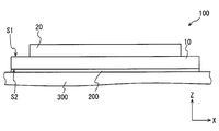
- the electronic device 100 is attached to the attached body 300 with a back surface S2 of the printed board 10 and a flat surface of the attached body 300 which will be described later facing each other.
- the electronic device 100 may be fixed to the attached body 300 with a bolt or the like.
- the electronic device 100 is preferably attached to the attached body 300 via a heat transfer member 200 such as heat radiation grease so that heat is efficiently transferred to the attached body 300.
- the heat transfer member 200 is disposed, for example, between the back surface S2 of the printed board 10 and the attached body 300.
- the arrangement, attachment, and function of the electronic device 100 are not limited to the above example.
- the electronic device 100 may be disposed around the engine or the torque converter in the engine room or outside the engine room. Furthermore, the electronic device 100 may not have a function as a control device for a vehicle.
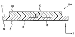
- the electronic device 100 includes a printed circuit board 10, a sealing resin 20, and a circuit component 30.
- the printed board 10 has a wiring 12 formed on a resin base material 11.
- the resin base material 11 includes a glass cloth and a resin.
- the resin base material 11 is obtained by impregnating a glass cloth with a resin.
- this resin for example, an epoxy resin containing an electrically insulating inorganic filler such as alumina or silica can be employed.
- the printed circuit board 10 includes a conductive conductor pattern and a via as the wiring 12.
- conductor patterns are laminated via a resin base material 11, and conductor patterns of different layers are electrically connected by vias.
- the printed circuit board 10 having a multilayer structure in which conductor patterns are stacked is employed.
- the printed circuit board 10 is not limited to the above example, and may be a printed circuit board 10 having a single layer structure in which no conductor pattern is stacked.
- the printed circuit board 10 has a predetermined thickness as shown in FIGS. 1 and 2, and the planar shape is rectangular. Further, as shown in FIG. 2, the printed circuit board 10 has one surface S1 and a back surface S2 that is the opposite surface of the one surface S1. Therefore, the printed circuit board 10 has one surface S1, a back surface S2, and four side walls.
- the planar shape is a shape in the XY plane.
- the thickness of each member for example, the thickness of the printed circuit board 10 corresponds to the length along the Z axis.
- the thickness of the printed circuit board 10 is equivalent to the space
- the planar shape of the printed circuit board 10 corresponds to the shape of one surface S1 in the XY plane and the shape of the back surface S2 in the XY plane.
- a printed circuit board 10 in which the longitudinal direction in the planar shape is parallel to the X axis and the short direction in the planar shape is parallel to the Y axis is employed.
- the longitudinal direction in the planar shape is simply referred to as the longitudinal direction
- the short direction in the planar shape is simply referred to as the lateral direction.
- the circuit component 30 is mounted on the printed board 10 and electrically connected to the wiring 12 as shown in FIG.
- the circuit component 30 is connected to the wiring 12 via a conductive connecting member such as solder. Note that a plurality of circuit components 30 may be mounted on the printed circuit board 10.
- the circuit component 30 is a component that constitutes a circuit together with the wiring 12 of the printed board 10, and an IC, a MOSFET, an IGBT, a diode, a resistor, a capacitor, or the like can be employed. Further, since the circuit component 30 is covered with the sealing resin 20, it can be adopted as a bare chip. In the present embodiment, an example in which the circuit component 30 is mounted only on the one surface S1 of the printed board 10 is employed.
- the sealing resin 20 is formed on the printed board 10 and seals the circuit component 30.
- the sealing resin 20 is electrically insulative, and is configured, for example, by containing a filler such as alumina or silica in an epoxy resin or the like.
- the sealing resin 20 can be molded by a transfer molding method, a compression molding method, or the like. For this reason, the sealing resin 20 can also be said to be a mold resin. Therefore, the electronic device 100 can also be said to be a mold package.
- the sealing resin 20 covers the circuit component 30 and a part of the one surface S1, and integrally covers them. Further, the sealing resin 20 covers the connection member together with the circuit component 30 and the one surface S ⁇ b> 1 while being in close contact with the connection member connecting the circuit component 30 and the printed board 10. Thus, since the circuit component 30 and the like are covered with the sealing resin 20, they are protected from the outside by the sealing resin 20.
- the sealing resin 20 has a thickness capable of covering the circuit component 30 and has a rectangular planar shape. Therefore, it can be said that the sealing resin 20 has a rectangular parallelepiped shape.
- the sealing resin 20 includes a first side 21 along the Y axis and a second side 22 along the X axis. In the sealing resin 20, the length Lx of the second side 22 is longer than the length Ly of the first side 21.
- the sealing resin 20 whose longitudinal direction is parallel to the X axis and whose lateral direction is parallel to the Y axis is employed.
- the printed circuit board 10 and the sealing resin 20 have a positional relationship in which the longitudinal directions of the printed circuit board 10 and the sealing resin 20 are parallel to each other. Note that the short direction and the long direction of the sealing resin 20 can be said to be two orthogonal directions in the planar shape of the sealing resin 20.
- the sealing resin 20 is provided only on one surface S1 of the printed board 10 is employed. Therefore, it can be said that the electronic device 100 has a half mold structure.
- the sealing resin 20 has an isotropic linear expansion coefficient ⁇ 3 in the XY plane.
- the printed circuit board 10 has anisotropy in the linear expansion coefficient in the XY plane.
- the printed circuit board 10 has a different linear expansion coefficient ⁇ 1 in the Y-axis direction and a linear expansion coefficient ⁇ 2 in the X-axis direction.
- the linear expansion coefficient ⁇ 1 is a linear expansion coefficient of the printed circuit board 10 along the short direction of the sealing resin 20.
- the linear expansion coefficient ⁇ 2 is a linear expansion coefficient of the printed circuit board 10 along the longitudinal direction of the sealing resin 20.
- the linear expansion coefficients ⁇ 1 and ⁇ 2 can be said to be linear expansion coefficients in two orthogonal directions on the printed circuit board 10.
- the printed circuit board 10 has a linear expansion coefficient in the direction along the short direction of the sealing resin 20 among the linear expansion coefficients in two orthogonal directions, and a line in the direction along the longitudinal direction of the sealing resin 20. It can be said that the expansion coefficient is ⁇ 2.
- the relationship between the linear expansion coefficients is ⁇ 3 ⁇ 2 ⁇ 1. That is, the electronic device 100 is configured such that the difference in linear expansion coefficient between the linear expansion coefficient ⁇ 3 and the linear expansion coefficient ⁇ 2 is smaller than the difference in linear expansion coefficient between the linear expansion coefficient ⁇ 3 and the linear expansion coefficient ⁇ 1. .
- the printed circuit board 10 can be obtained by cutting a base substrate on which a plurality of printed circuit boards 10 are continuously formed. That is, it can be said that the base substrate is formed with a plurality of regions that can become the printed circuit board 10. Further, the base substrate has different linear expansion coefficients in two orthogonal directions on the printed circuit board 10 depending on the cutting direction. Therefore, it can be said that the base substrate can satisfy ⁇ 2 ⁇ 1 depending on the cutting direction.
- the sealing resin 20 is formed on the printed circuit board 10 so that the relationship between the linear expansion coefficients is ⁇ 3 ⁇ 2 ⁇ 1.
- the printed circuit board 10 is sealed.
- the sealing resin 20 is formed so that the longitudinal direction of the resin 20 is parallel to the X axis and the short side direction is parallel to the Y axis.
- the sealing resin 20 can adjust the linear expansion coefficient ⁇ 3 depending on the amount of filler. Specifically, the sealing resin 20 can reduce the linear expansion coefficient ⁇ 3 by increasing the filler amount, and can increase the linear expansion coefficient ⁇ 3 by reducing the filler amount. Therefore, in the electronic device 100, for example, the linear expansion coefficient ⁇ 3 of the sealing resin 20 is adjusted with the linear expansion coefficient ⁇ 2 as a reference so as to be smaller than the linear expansion coefficient ⁇ 2, so that the relationship between the linear expansion coefficients is ⁇ 3 ⁇ 2. ⁇ 1.
- the warp of the electronic device 100 which is a mold package is determined by the curing shrinkage of the sealing resin 20 immediately after molding and the difference in linear expansion coefficient between the sealing resin 20 and the printed circuit board 10.
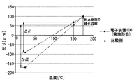
- the curing shrinkage As shown in FIG. 4, in the electronic device 100, it is preferable to make the curing shrinkage as small as possible in order to reduce the warp at a high temperature at which heat dissipation characteristics are desired.
- the electronic device 100 in order to reduce the warp amplitude in the cold environment, it is necessary to reduce the difference in linear expansion coefficient between the sealing resin 20 and the printed circuit board 10, that is, to increase the linear expansion coefficient of the sealing resin 20. is there.
- the comparative example is a mold package in which the relationship between the linear expansion coefficients is not as described above. However, each component in the comparative example is described with the same name as the electronic device 100 for convenience.
- the cold environment is an installation environment as described above.
- the warp amplitude can also be said to be the amount of change in warp of the electronic device 100 when the temperature of the mounting environment changes. Therefore, the warp amplitude in the cold environment is, for example, the warp of the electronic device 100 when the temperature of the mounting environment is normal temperature (for example, 25 ° C.) and the temperature of the mounting environment is high (for example, 150 ° C.). This corresponds to a difference from the warp of the electronic device 100.
- ⁇ d1 in FIG. 4 is the warp amplitude of the electronic device 100, and the difference between the warp of the electronic device 100 when the temperature of the mounting environment is normal and the warp of the electronic device 100 when the temperature of the mounting environment is high.
- ⁇ d2 in FIG. 4 is the warp amplitude of the comparative example, which is the difference between the warp of the comparative example when the temperature of the mounting environment is room temperature and the warp of the comparative example when the temperature of the mounting environment is high
- the warp shape of the electronic device 100 and the comparative example is the first warp shape of FIG. 5 when along the plus side, and the second warp shape of FIG. 5 when along the minus side. It can be said that the first warp shape is a smile warp. On the other hand, the second warp shape can be said to be a cry warp.
- the back surface S2 and the flat surface of the mounted body 300 are not parallel. For this reason, when the electronic device 100 is warped as described above, the attachment property to the attached body 300 is worse than when the electronic device 100 is not warped.
- the electronic device 100 warps in the second warp shape, there is a possibility that a space is formed between the electronic device 100 and the mounted body 300.
- the electronic device 100 when a space is formed between the electronic device 100 and the mounted body 300, heat dissipation is reduced.
- the printed circuit board 10 and the attached body 300 may directly contact each other by pushing the heat transfer member 200 provided between the electronic device 100 and the attached body 300. There is.
- the heat dissipation performance is lower than when the heat transfer member 200 is interposed between the printed circuit board 10 and the attached body 300.
- a special design such as containing a curing agent in the sealing resin 20 is used. Necessary. Further, the sealing resin 20 is more expensive when a special design is required than when a special design is not required.
- the printed circuit board 10 is provided with a sealing resin 20 having a rectangular planar shape.
- the sum of the warp in the direction along the short direction of the sealing resin 20 and the warp in the direction along the longitudinal direction of the sealing resin 20 is the entire warp.
- the entire warp of the electronic device 100 is greatly influenced by the warp in the direction along the longitudinal direction of the sealing resin 20. Note that the warpage in the direction along the short direction of the sealing resin 20 and the warpage in the direction along the longitudinal direction of the sealing resin 20 are warpages of the electronic device 100.
- the electronic device 100 is configured such that the difference in linear expansion coefficient between the linear expansion coefficient ⁇ 3 and the linear expansion coefficient ⁇ 2 is smaller than the difference in linear expansion coefficient between the linear expansion coefficient ⁇ 3 and the linear expansion coefficient ⁇ 1 as described above. Has been. For this reason, the electronic device 100 can suppress the warp in the direction along the longitudinal direction, which has a large influence on the overall warp of the electronic device 100. Therefore, the warp of the entire electronic device 100 can be suppressed. As described above, since the overall warpage of the electronic device 100 can be suppressed by making the relationship between the linear expansion coefficients as described above, the warpage can be easily suppressed. In addition, since the electronic device 100 does not require a special design as described above, it can be made cheaper than a case where a special design is required.
- the electronic device 100 can suppress the first warp shape and the second warp shape. Therefore, the electronic device 100 can suppress the attachment property to the attachment target 300 from being deteriorated. Furthermore, the electronic device 100 can suppress a decrease in heat dissipation.
- the mold package will grow in size due to the multi-functionality of mounted functions.
- the warpage of the mold package becomes more prominent as the size of the package increases.
- the electronic device 100 can suppress the warp as described above, the warp can be suppressed even if the physique is increased.
- the physique here is the magnitude
- the sealing resin 20 is also isotropic with respect to the Young's modulus E3.
- the printed circuit board 10 has anisotropy with respect to Young's modulus.
- the printed circuit board 10 has a different Young's modulus E1 in the Y-axis direction and a Young's modulus E2 in the X-axis direction.
- the magnitude relationship of Young's modulus is opposite to the magnitude relationship of the linear expansion coefficient. Therefore, in the electronic device 100, the relationship of E3> E2> E1 is satisfied.
- the electronic device 100 can achieve the above-described effect by setting the relationship between the Young's moduli to E3> E2> E1.
- the Young's modulus E1 is the Young's modulus of the printed circuit board 10 along the short direction of the sealing resin 20.
- the Young's modulus E2 is the Young's modulus of the printed circuit board 10 along the longitudinal direction of the sealing resin 20.
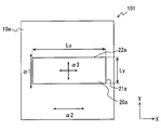
- the electronic device 101 according to the second embodiment will be described with reference to FIG.
- the short direction of the printed circuit board 10a and the longitudinal direction of the sealing resin 20a are parallel, and the long direction of the printed circuit board 10a and the short direction of the sealing resin 20a are parallel. Different from 100.
- the sealing resin 20a includes a first side 21a along the Y axis and a second side 22a along the X axis.
- the length Lx of the second side 22a is longer than the length Ly of the first side 21a.
- the sealing resin 20a has a linear expansion coefficient ⁇ 3.
- the sealing resin 20a is the same as the sealing resin 20.
- the printed circuit board 10a has a different linear expansion coefficient ⁇ 1 in the Y-axis direction and a linear expansion coefficient ⁇ 2 in the X-axis direction, as in the above embodiment.
- the linear expansion coefficient ⁇ 1 is a linear expansion coefficient of the printed circuit board 10a along the short direction of the sealing resin 20a.
- the linear expansion coefficient ⁇ 2 is a linear expansion coefficient of the printed circuit board 10a along the longitudinal direction of the sealing resin 20a.
- the printed circuit board 10a has a linear expansion coefficient ⁇ 1 that is a linear expansion coefficient in the longitudinal direction of the printed circuit board 10a, and a linear expansion coefficient ⁇ 2 that is a linear expansion coefficient in the short direction of the printed circuit board 10a.
- each linear expansion coefficient satisfies the relationship of ⁇ 3 ⁇ 2 ⁇ 1.
- the electronic device 101 configured as described above can achieve the same effects as the electronic device 100.
- the sealing resin 20a is provided on one surface S1 of the printed board 10a, and the sealing resin may also be provided on the back surface S2 opposite to the one surface S1.
- the sealing resin on the back surface S2 side is attached to the attached body 300 in a state of facing the attached body 300.
- the electronic device 101 may be attached to the attached body 300 via the heat transfer member 200 between the sealing resin on the back surface S2 side and the attached body 300.
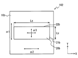
- the electronic device 102 according to the third embodiment will be described with reference to FIG.
- the electronic device 102 is different from the electronic device 100 in that the planar shape of the printed circuit board 10b is a square.
- the sealing resin 20b includes a first side 21b along the Y axis and a second side 22b along the X axis.
- the length Lx of the second side 22b is longer than the length Ly of the first side 21b.
- the sealing resin 20b has a linear expansion coefficient ⁇ 3.
- the sealing resin 20b is the same as the sealing resin 20.
- the printed circuit board 10b has a different linear expansion coefficient ⁇ 1 in the Y-axis direction and a linear expansion coefficient ⁇ 2 in the X-axis direction, as in the above embodiment.
- linear expansion coefficient (alpha) 1 is a linear expansion coefficient of the printed circuit board 10b along the transversal direction of the sealing resin 20b.
- the linear expansion coefficient ⁇ 2 is a linear expansion coefficient of the printed circuit board 10b along the longitudinal direction of the sealing resin 20b.
- each linear expansion coefficient satisfies the relationship of ⁇ 3 ⁇ 2 ⁇ 1.
- the electronic device 102 configured as described above can achieve the same effects as the electronic device 100.
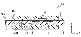
- the electronic device 103 according to the fourth embodiment will be described with reference to FIGS. 9 and 10.
- the electronic device 103 is different from the electronic device 100 in that the sealing resin 20c is provided on one surface S1 of the printed board 10c and the sealing resin 20d is provided on the back surface S2.
- circuit components 30 are mounted on both the one surface S1 and the back surface S2 of the printed circuit board 10c.
- the circuit component 30 for example, a first circuit component is provided on the one surface S1 side, and a second circuit component is provided on the back surface S2 side.
- the electronic device 103 includes sealing resin 20c having a rectangular planar shape provided on one surface S1 and sealing resin 20d having a rectangular planar shape provided on the back surface S2 as sealing resin.
- the sealing resin 20c corresponds to the first sealing resin.
- the sealing resin 20d corresponds to a second sealing resin.
- the constituent materials of the sealing resins 20c and 20d are the same.
- the sealing resin 20c includes a first side 21c along the Y axis and a second side 22c along the X axis.
- the length Lx of the second side 22c is longer than the length Ly of the first side 21c.
- the sealing resin 20c has a linear expansion coefficient ⁇ 3.
- the sealing resin 20c is the same as the sealing resin 20.
- the sealing resin 20d includes a first side along the Y axis and a second side along the X axis, similarly to the sealing resin 20c.
- the length of the second side is longer than the length of the first side.
- the sealing resin 20d has a second side length similar to the second side 22c of the sealing resin 20c, and a first side length similar to the first side 21c of the sealing resin 20c.
- the sealing resin 20d has a linear expansion coefficient ⁇ 3.
- an example is employed in which the sealing resin 20c and the sealing resin 20d are opposed to each other with the printed circuit board 10c interposed therebetween.
- the printed circuit board 10c has a different linear expansion coefficient ⁇ 1 in the Y-axis direction and a linear expansion coefficient ⁇ 2 in the X-axis direction, as in the above embodiment.
- linear expansion coefficient (alpha) 1 is a linear expansion coefficient of the printed circuit board 10c along the transversal direction of sealing resin 20c, 20d.
- the linear expansion coefficient ⁇ 2 is a linear expansion coefficient of the printed circuit board 10c along the longitudinal direction of the sealing resins 20c and 20d.
- each linear expansion coefficient satisfies the relationship of ⁇ 3 ⁇ 2 ⁇ 1.
- the electronic device 103 configured as described above can achieve the same effects as the electronic device 100.
- the sealing resin 20d may be provided on one surface S1, and the sealing resin 20c may be provided on the back surface S2.
- the electronic device 104 according to the fifth embodiment will be described with reference to FIGS. 11 and 12.
- the electronic device 104 is different from the electronic device 103 in that the sealing resin 20e provided on the one surface S1 and the sealing resin 20f provided on the back surface S2 are different in size.
- the size is the size on the XY plane and can be said to be the area on the XY plane.
- circuit components 30 are mounted on both the one surface S1 and the back surface S2 of the printed circuit board 10d.
- the electronic device 104 includes a sealing resin 20e having a rectangular planar shape provided on one surface S1 and a sealing resin 20f having a rectangular planar shape provided on the back surface S2 as the sealing resin.
- the sealing resin 20e corresponds to the first sealing resin.
- the sealing resin 20f corresponds to a second sealing resin.
- the constituent materials of the sealing resins 20e and 20f are the same.
- the sealing resin 20e includes a first side 21e along the Y axis and a second side 22e along the X axis.
- the length Lx of the second side 22e is longer than the length Ly of the first side 21e.
- the sealing resin 20e has a linear expansion coefficient ⁇ 3.
- the sealing resin 20e is the same as the sealing resin 20.
- the sealing resin 20f includes a first side 21f along the Y axis and a second side 22f along the X axis.
- the length Ly1 of the first side 21f is longer than the length Lx1 of the second side 22f.
- the sealing resin 20f has a linear expansion coefficient ⁇ 3.
- the length relationships are Lx> Ly, Lx1 ⁇ Ly1, and Lx> Ly1.
- the length Lx in the longitudinal direction of the sealing resin 20e is longer than the length Ly1 in the longitudinal direction of the sealing resin 20f. Therefore, the second side 22e of the sealing resin 20e is the longest in each side 21e, 22e, 21f, 22f of the sealing resin 20e, 20f. For this reason, in the electronic device 104, the second side 22e is regarded as a side in the longitudinal direction of the sealing resin.
- the printed circuit board 10d has a different linear expansion coefficient ⁇ 1 in the Y-axis direction and a linear expansion coefficient ⁇ 2 in the X-axis direction, as in the above embodiment.
- the linear expansion coefficient ⁇ 1 is a linear expansion coefficient of the printed circuit board 10d along the short direction of the sealing resin 20e.
- the linear expansion coefficient ⁇ 2 is a linear expansion coefficient of the printed circuit board 10d along the longitudinal direction of the sealing resin 20e.
- each linear expansion coefficient satisfies the relationship of ⁇ 3 ⁇ 2 ⁇ 1.
- the electronic device 104 configured as described above can achieve the same effect as the electronic device 103.
- the electronic device 104 may be provided with the sealing resin 20f on one surface S1 and the sealing resin 20e on the back surface S2.
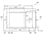
- the electronic device 105 according to the sixth embodiment will be described with reference to FIGS. 13 and 14. As shown in FIG. 13, the electronic device 105 is different from the electronic device 104 in that the planar shape of one sealing resin 20 h is a positive direction. In the electronic device 105, as shown in FIG. 14, circuit components 30 are mounted on both the one surface S1 and the back surface S2 of the printed circuit board 10e.
- the electronic device 105 includes a sealing resin 20g having a rectangular planar shape provided on one surface S1 and a sealing resin 20h having a square planar shape provided on the back surface S2 as the sealing resin.
- the sealing resin 20g corresponds to the first sealing resin.
- the sealing resin 20h corresponds to a second sealing resin.
- the constituent materials of the sealing resins 20g and 20h are the same.
- the sealing resin 20g includes a first side 21g along the Y axis and a second side 22g along the X axis.
- the length Lx of the second side 22g is longer than the length Ly of the first side 21g.
- the sealing resin 20g has a linear expansion coefficient ⁇ 3.
- the sealing resin 20g is the same as the sealing resin 20.
- the sealing resin 20h includes a first side 21h along the Y axis and a second side 22h along the X axis. Since the planar shape of the sealing resin 20h is square, the length Ly1 of the first side 21h and the length Lx1 of the second side 22h are the same. Further, the sealing resin 20h has a linear expansion coefficient ⁇ 3.
- the planar shape of the sealing resin 20g is rectangular
- the planar shape of the sealing resin 20h is square
- the longitudinal direction of the sealing resin 20g is the second side 22g.
- the second side 22g is regarded as a side in the longitudinal direction of the sealing resin. That is, in the electronic device 105, the longitudinal direction of the sealing resin 20g having a rectangular planar shape is regarded as the side in the longitudinal direction of the sealing resin.
- the printed circuit board 10e has a different linear expansion coefficient ⁇ 1 in the Y-axis direction and a linear expansion coefficient ⁇ 2 in the X-axis direction, as in the above embodiment.
- the linear expansion coefficient ⁇ 1 is a linear expansion coefficient of the printed circuit board 10e along the short direction of the sealing resin 20g.
- the linear expansion coefficient ⁇ 2 is a linear expansion coefficient of the printed circuit board 10e along the longitudinal direction of the sealing resin 20g.
- each linear expansion coefficient satisfies the relationship of ⁇ 3 ⁇ 2 ⁇ 1.
- the electronic device 105 configured as described above can achieve the same effects as the electronic device 104.
- the sealing resin 20h may be provided on one surface S1, and the sealing resin 20g may be provided on the back surface S2.
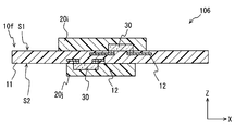
- the electronic device 106 according to the seventh embodiment will be described with reference to FIGS. 15 and 16.
- the electronic device 106 is different from the electronic device 105 in the size relationship between the sealing resin 20 i having a positive planar shape and the sealing resin 20 j having a rectangular planar shape.
- the size is the size on the XY plane and can be said to be the area on the XY plane.
- circuit components 30 are mounted on both the one surface S1 and the back surface S2 of the printed circuit board 10f.
- the electronic device 106 includes a sealing resin 20i having a square planar shape provided on one surface S1 and a sealing resin 20j having a rectangular planar shape provided on the back surface S2, as sealing resins. Including.
- the sealing resin 20i corresponds to the second sealing resin.
- the sealing resin 20j corresponds to the first sealing resin.
- the constituent materials of the sealing resins 20i and 20j are the same.
- the sealing resin 20 i includes a first side 21 i along the Y axis and a second side 22 i along the X axis. Since the sealing resin 20i has a square planar shape, the length Ly of the first side 21i and the length Lx of the second side 22i are the same. Further, the sealing resin 20i has a linear expansion coefficient ⁇ 3.
- the sealing resin 20j includes a first side 21j along the Y axis and a second side 22j along the X axis.
- the length Lx1 of the second side 22j is longer than the length Ly1 of the first side 21j.
- the sealing resin 20j has a linear expansion coefficient ⁇ 3.
- both sides 21i and 22i of the sealing resin 20i are longer than the second side 22j of the sealing resin 20j.
- the planar shape of the sealing resin 20j is rectangular, the planar shape of the sealing resin 20i is square, and the longitudinal direction of the sealing resin 20j is the second side 22j.
- the second side 22j is regarded as a side in the longitudinal direction of the sealing resin. That is, in the electronic device 106, the longitudinal direction of the sealing resin 20j having a rectangular planar shape is regarded as the side in the longitudinal direction of the sealing resin.
- the printed circuit board 10f has a different linear expansion coefficient ⁇ 1 in the Y-axis direction and a linear expansion coefficient ⁇ 2 in the X-axis direction, as in the above embodiment.
- the linear expansion coefficient ⁇ 1 is a linear expansion coefficient of the printed board 10e along the short direction of the sealing resin 20j.
- the linear expansion coefficient ⁇ 2 is a linear expansion coefficient of the printed circuit board 10e along the longitudinal direction of the sealing resin 20j.
- each linear expansion coefficient satisfies the relationship of ⁇ 3 ⁇ 2 ⁇ 1.
- the electronic device 106 configured as described above can achieve the same effect as the electronic device 105.
- the sealing resin 20j may be provided on one surface S1, and the sealing resin 20i may be provided on the back surface S2.
Landscapes
- Engineering & Computer Science (AREA)
- Manufacturing & Machinery (AREA)
- Microelectronics & Electronic Packaging (AREA)
- Structures Or Materials For Encapsulating Or Coating Semiconductor Devices Or Solid State Devices (AREA)
- Non-Metallic Protective Coatings For Printed Circuits (AREA)
Abstract
電子装置(100)は、樹脂基材に配線が形成されたプリント基板(10)と、プリント基板(10)に実装され、配線と電気的に接続された回路部品と、プリント基板(10)に形成され、回路部品を封止している、平面形状が矩形状の封止樹脂(20)と、を備えている。電子装置(100)は、封止樹脂(20)の短手方向に沿うプリント基板(10)の線膨張係数α1と、封止樹脂(20)の長手方向に沿うプリント基板の線膨張係数α2と、封止樹脂(20)の線膨張係数α3との関係がα3<α2<α1である。
Description
本出願は、2016年4月15日に出願された日本出願番号2016-81712号に基づくもので、ここにその記載内容を援用する。
本開示は、プリント基板に封止樹脂が設けられた電子装置に関する。
従来、プリント基板に封止樹脂が設けられた電子装置の一例として、特許文献1に開示されたものがある。
電子装置は、プリント基板と封止樹脂との線膨張係数の差によって反りが生じる。一般的に、電子装置の反りを小さくする場合は、封止樹脂の線膨張係数を調整する。このため、電子装置においては、プリント基板と封止樹脂との線膨張係数の差を小さくする場合、封止樹脂の線膨張係数を大きくすることになる。しかしながら、封止樹脂の線膨張係数が大きくなるにつれて硬化収縮率が高くなり、電子装置において、反りを抑制するのが難しい。
本開示は、容易に反りを抑制できる電子装置を提供することを目的とする。
本開示の一態様によれば、電子装置は、樹脂基材と、樹脂基材に形成された配線とを有するプリント基板と、プリント基板に実装され、配線と電気的に接続された回路部品と、プリント基板上に設けられ、回路部品を封止している、平面形状が矩形状の封止樹脂と、を備える。さらに、封止樹脂の短手方向に沿うプリント基板の線膨張係数α1と、封止樹脂の長手方向に沿うプリント基板の線膨張係数α2と、封止樹脂の線膨張係数α3との関係がα3<α2<α1である。
上記電子装置において、プリント基板に、平面形状が矩形状の封止樹脂が設けられている。このような電子装置においては、上記短手方向に沿う方向の反りと、上記長手方向に沿う方向の反りとの和が、全体の反りとなる。また、通常、電子装置の全体の反りは、長手方向に沿う方向の反りの影響が大きい。
そこで、上記電子装置においては、線膨張係数α3と線膨張係数α1との線膨張係数差よりも、線膨張係数α3と線膨張係数α2との線膨張係数差が小さくなるように構成されている。このため、電子装置の全体の反りへの影響が大きい、長手方向に沿う方向の反りを抑制できる。よって、電子装置の全体の反りを抑制できる。このように、各線膨張係数の関係を上記のようにすることで全体の反りを抑制できるため、容易に反りを抑制できる。
本開示についての上記目的およびその他の目的、特徴や利点は、添付の図面を参照しながら下記の詳細な記述により、より明確になる。
第1実施形態における電子装置の概略構成を示す平面図である。
図1のII-II線に沿う断面図である。
第1実施形態における電子装置の搭載構造を示す側面図である。
第1実施形態の電子装置と比較例の電子装置における、温度と反りの関係を示すグラフである。
電子装置の反り形状を示す図である。
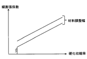
封止樹脂の線膨張係数と硬化収縮率との関係を示すグラフである。
第2実施形態における電子装置の概略構成を示す平面図である。
第3実施形態における電子装置の概略構成を示す平面図である。
第4実施形態における電子装置の概略構成を示す平面図である。
図9のX-X線に沿う断面図である。
第5実施形態における電子装置の概略構成を示す平面図である。
図11のXII-XII線に沿う断面図である。
第6実施形態における電子装置の概略構成を示す平面図である。
図13のXIV-XIV線に沿う断面図である。
第7実施形態における電子装置の概略構成を示す平面図である。
図15のXVI-XVI線に沿う断面図である。
以下において、図面を参照しながら、開示を実施するための複数の形態を説明する。各形態において、先行する形態で説明した事項に対応する部分には同一の参照符号を付して重複する説明を省略する場合がある。各形態において、構成の一部のみを説明している場合は、構成の他の部分については先行して説明した他の形態を参照し適用することができる。
(第1実施形態)
図1~図6を用いて、第1実施形態の電子装置100に関して説明する。電子装置100は、例えば車両用の制御装置としての機能を有しており、車両のエンジンルームなどに搭載される。エンジンルームには、例えばエンジンとトルクコンバータなどが配置されている。このため、電子装置100は、エンジンやトルクコンバータと同じ空間に配置されていると言える。よって、電子装置100は、-40℃~120℃程度の範囲や、-40℃~150℃程度の範囲や、25℃~120℃程度の範囲や、25℃~150℃程度の範囲などで温度が変化する搭載環境に搭載される。つまり、電子装置100は、マイナス数十度からプラス百度を超える範囲や、常温からプラス百度を超える範囲で温度が変化する搭載環境に搭載されると言える。
図1~図6を用いて、第1実施形態の電子装置100に関して説明する。電子装置100は、例えば車両用の制御装置としての機能を有しており、車両のエンジンルームなどに搭載される。エンジンルームには、例えばエンジンとトルクコンバータなどが配置されている。このため、電子装置100は、エンジンやトルクコンバータと同じ空間に配置されていると言える。よって、電子装置100は、-40℃~120℃程度の範囲や、-40℃~150℃程度の範囲や、25℃~120℃程度の範囲や、25℃~150℃程度の範囲などで温度が変化する搭載環境に搭載される。つまり、電子装置100は、マイナス数十度からプラス百度を超える範囲や、常温からプラス百度を超える範囲で温度が変化する搭載環境に搭載されると言える。
電子装置100の取り付け対象である被取付体300は、エンジンやトルクコンバータにおける金属ケースなどの金属部分を採用できる。この金属部分は、電子装置100から発せられた熱を放熱するための放熱部材として機能する。被取付体300は、エンジンやトルクコンバータにおける金属部分とは異なるヒートシンクであっても採用できる。電子装置100は、後程説明するプリント基板10の裏面S2と被取付体300の平坦面とが対向した状態で、被取付体300に取り付けられる。電子装置100は、ボルトなどで被取付体300に固定されてもよい。
電子装置100は、図3に示すように、被取付体300に効率よく熱伝達されるように、放熱グリスなどの熱伝達部材200を介して被取付体300に取り付けられると好ましい。熱伝達部材200は、例えば、プリント基板10の裏面S2と被取付体300との間に配置される。
しかしながら、本開示において、電子装置100の配置や取付け、機能は上記例に限定されない。電子装置100は、エンジンルームにおけるエンジンやトルクコンバータの周辺、又はエンジンルーム外に配置されていてもよい。さらに、電子装置100は、車両用の制御装置としての機能を有していなくてもよい。
図1、図2、図3に示すように、電子装置100は、プリント基板10、封止樹脂20、回路部品30を備えて構成されている。
プリント基板10は、図2に示すように、樹脂基材11に配線12が形成されている。樹脂基材11は、ガラスクロスと樹脂とを含んで構成されている。言い換えると、樹脂基材11は、ガラスクロスに樹脂を含浸させたものである。この樹脂としては、例えば、アルミナやシリカなどの電気絶縁性を有する無機フィラーが含有しているエポキシ樹脂などを採用できる。
プリント基板10は、配線12として導電性の導体パターンとビアとを含んでいる。プリント基板10は、導体パターンが樹脂基材11を介して積層されており、異なる層の導体パターンがビアによって電気的に接続されている。このように、本実施形態では、導体パターンが積層された多層構造のプリント基板10を採用している。しかしながら、本開示においては、プリント基板10は上記例に限定されず、導体パターンが積層されていない単層構造のプリント基板10であってもよい。
プリント基板10は、図1、図2に示すように、所定の厚みを有しており、平面形状が矩形状をなしている。また、プリント基板10は、図2に示すように、一面S1と、一面S1の反対面である裏面S2を有している。よって、プリント基板10は、一面S1と裏面S2と四つの側壁とを有している。
本開示において、平面形状とは、XY平面における形状である。また、各部材の厚み、例えば、プリント基板10の厚みとは、Z軸に沿う長さに相当する。また、プリント基板10の厚みは、一面S1と裏面S2との間隔に相当する。プリント基板10の平面形状は、XY平面における一面S1の形状、及びXY平面における裏面S2の形状に相当する。本実施形態では、平面形状における長手方向がX軸と平行で、平面形状における短手方向がY軸と平行であるプリント基板10を採用している。以下においては、平面形状における長手方向を単に長手方向、平面形状における短手方向を単に短手方向とも記載する。
回路部品30は、図2に示すように、プリント基板10に実装され、配線12と電気的に接続されている。回路部品30は、はんだなどの導電性の接続部材を介して、配線12と接続されている。なお、プリント基板10には、複数の回路部品30が実装されていてもよい。
回路部品30は、プリント基板10の配線12とともに回路を構成する部品であり、IC、MOSFET、IGBT、ダイオード、抵抗、コンデンサなどを採用できる。また、回路部品30は、封止樹脂20で覆われているため、ベアチップでも採用できる。なお、本実施形態では、プリント基板10の一面S1にのみ回路部品30が実装されている例を採用している。
封止樹脂20は、図2に示すように、プリント基板10上に形成され、回路部品30を封止している。封止樹脂20は、電気絶縁性であり、例えば、エポキシ樹脂などに、アルミナやシリカなどのフィラーが含有されて構成されている。封止樹脂20は、トランスファーモールド法やコンプレッションモールド法等により成形できる。このため、封止樹脂20は、モールド樹脂とも言える。よって、電子装置100は、モールドパッケージとも言える。
封止樹脂20は、回路部品30と、一面S1の一部に密着しつつ、これらを一体的に覆っている。また、封止樹脂20は、回路部品30とプリント基板10とを接続している接続部材に密着しつつ、回路部品30や一面S1とともに接続部材を覆っている。このように、回路部品30などは、封止樹脂20で覆われているため、封止樹脂20によって外部から保護されている。
封止樹脂20は、図1、図2に示すように、回路部品30を覆うことができる厚みを有し、平面形状が矩形状である。よって、封止樹脂20は、直方体形状と言える。封止樹脂20は、Y軸に沿う第1辺21と、X軸に沿う第2辺22とを含んでいる。封止樹脂20は、第2辺22の長さLxが第1辺21の長さLyよりも長い。このように、本実施形態では、長手方向がX軸と平行で、短手方向がY軸と平行である封止樹脂20を採用している。プリント基板10と封止樹脂20は、互いの長手方向どうしが並行であり、且つ短手方向どうしが並行である位置関係となっている。なお、封止樹脂20の短手方向と長手方向は、封止樹脂20の平面形状における直交する二方向とも言える。
本実施形態では、プリント基板10の一面S1にのみ封止樹脂20が設けられている例を採用している。よって、電子装置100は、ハーフモールド構造をなしていると言える。
ここで、プリント基板10と封止樹脂20の線膨張係数に関して説明する。封止樹脂20は、XY平面における線膨張係数α3が等方性である。これに対して、プリント基板10は、XY平面における線膨張係数に異方性を有している。
つまり、プリント基板10は、Y軸方向の線膨張係数α1と、X軸方向の線膨張係数α2とが異なる。線膨張係数α1は、封止樹脂20の短手方向に沿うプリント基板10の線膨張係数である。一方、線膨張係数α2は、封止樹脂20の長手方向に沿うプリント基板10の線膨張係数である。線膨張係数α1、α2は、プリント基板10における直交する二方向の線膨張係数と言える。また、プリント基板10は、直交する二方向の線膨張係数のうち、封止樹脂20の短手方向に沿う方向の線膨張係数がα1であり、封止樹脂20の長手方向に沿う方向の線膨張係数がα2であると言える。
そして、電子装置100においては、各線膨張係数の関係がα3<α2<α1となっている。つまり、電子装置100においては、線膨張係数α3と線膨張係数α1との線膨張係数差よりも、線膨張係数α3と線膨張係数α2との線膨張係数差が小さくなるように構成されている。
プリント基板10は、複数のプリント基板10が連続的に形成されたベース基板を切断して切り出されたものを用いることができる。つまり、ベース基板は、プリント基板10となりうる領域が複数個所に形成されたものと言える。また、ベース基板は、切断方向によって、プリント基板10における直交する二方向の線膨張係数が異なる。このため、ベース基板は、切断方向によって、α2<α1とすることができる、とも言える。
そして、電子装置100において、線膨張係数の関係がα3<α2<α1となるように、プリント基板10に対して封止樹脂20が形成されている。例えば、図1に示すように、X軸方向に線膨張係数α2を、Y軸方向に線膨張係数α1を有するようにプリント基板10が配置される場合、このプリント基板10に対して、封止樹脂20の長手方向がX軸と平行で、且つ短手方向がY軸と平行となるように封止樹脂20を形成する。
また、封止樹脂20は、フィラー量によって線膨張係数α3を調整できる。具体的には、封止樹脂20は、フィラー量を増やすことで線膨張係数α3を小さくでき、フィラー量を減らすことで線膨張係数α3を大きくできる。よって、電子装置100において、例えば、線膨張係数α2を基準として、封止樹脂20の線膨張係数α3を調整して線膨張係数α2よりも小さくすることで、各線膨張係数の関係をα3<α2<α1とすることができる。
ところで、モールドパッケージである電子装置100の反りは、成形直後における封止樹脂20の硬化収縮と、封止樹脂20とプリント基板10の線膨張係数差によって決まる。図4に示すように、電子装置100において、放熱特性を確保したい高温時の反りを小さくするには硬化収縮をできるだけ小さくすることが好ましい。一方、電子装置100において、冷熱環境下での反り振幅を小さくするには、封止樹脂20とプリント基板10の線膨張係数差を小さく、つまり封止樹脂20の線膨張係数を大きくする必要がある。図4は、本実施形態の電子装置100と比較例の電子装置(以下、比較例)における、温度と反りの関係を示すグラフである。比較例は、線膨張係数の関係が上記のようになっていないモールドパッケージである。しかしながら、比較例における各構成要素は、便宜的に、電子装置100と同じ名称で記載する。
なお、冷熱環境とは、上記のような搭載環境である。また、反り振幅とは、搭載環境の温度が変化した場合における電子装置100の反りの変化量とも言える。よって、冷熱環境下での反り振幅は、例えば、搭載環境の温度が常温(例えば25℃)である場合の電子装置100の反りと、搭載環境の温度が高温(例えば150℃)である場合の電子装置100の反りとの差などに相当する。図4のΔd1は、電子装置100の反り振幅であり、搭載環境の温度が常温である場合の電子装置100の反りと、搭載環境の温度が高温である場合の電子装置100の反りとの差である。図4のΔd2は、比較例の反り振幅であり、搭載環境の温度が常温である場合の比較例の反りと、搭載環境の温度が高温である場合の比較例の反りとの差である。
また、電子装置100や比較例の反り形状は、プラス側に沿った場合に図5の第1反り形状となり、マイナス側に沿った場合に図5の第2反り形状となる。なお、第1反り形状は、スマイル反りと言える。一方、第2反り形状は、クライ反りと言える。電子装置100や比較例は、上記のように反った場合、裏面S2と被取付体300の平坦面とが平行ではなくなる。このため、電子装置100は、上記のように反った場合、反ってない場合よりも被取付体300への取付性が悪くなる。
また、電子装置100は、第2反り形状に反った場合、被取付体300との間に空間が形成される可能性がある。電子装置100は、被取付体300との間に空間が形成された場合、放熱性が低下する。一方、電子装置100は、第1反り形状に反った場合、被取付体300との間に設けられた熱伝達部材200を押しのけて、プリント基板10と被取付体300とが直接接触する可能性がある。電子装置100は、プリント基板10と被取付体300とが直接接触した場合、プリント基板10と被取付体300との間に熱伝達部材200を介在している場合よりも放熱性が低下する。
しかしながら、図6に示すように、封止樹脂20の硬化収縮を小さくすることと、封止樹脂20の線膨張係数を大きくすることは、背反事項である。また、図6に示すように、封止樹脂20は、成形後の封止樹脂20の品質を確保するために、線膨張係数をフィラー量で調整できる範囲、すなわち材料調整幅が決まっている。
このため、封止樹脂20の硬化収縮を小さくすることと、封止樹脂20の線膨張係数を大きくすることを両立させるためには、封止樹脂20に硬化剤を含有させるなど特殊な設計が必要となる。また、封止樹脂20は、特殊な設計が必要な場合、特殊な設計が必要ない場合よりも高価になってしまう。
なお、電子装置100においては、プリント基板10に、平面形状が矩形状の封止樹脂20を設けている。このような電子装置100は、封止樹脂20の短手方向に沿う方向の反りと、封止樹脂20の長手方向に沿う方向の反りとの和が、全体の反りとなる。また、通常、電子装置100の全体の反りは、封止樹脂20の長手方向に沿う方向の反りの影響が大きい。なお、ここでの、封止樹脂20の短手方向に沿う方向の反りや、封止樹脂20の長手方向に沿う方向の反りは、電子装置100の反りである。
そこで、電子装置100は、上記のように線膨張係数α3と線膨張係数α1との線膨張係数差よりも、線膨張係数α3と線膨張係数α2との線膨張係数差が小さくなるように構成されている。このため、電子装置100は、電子装置100の全体の反りへの影響が大きい、長手方向に沿う方向の反りを抑制できる。よって、電子装置100の全体の反りを抑制できる。このように、各線膨張係数の関係を上記のようにすることで、電子装置100の全体の反りを抑制できるため、容易に反りを抑制できる。また、電子装置100は、上記のような特殊な設計が必要ないため、特殊な設計が必要な場合よりも安価にすることができる。
このように、電子装置100において、反りを抑制できる。このため、電子装置100は、第1反り形状及び第2反り形状となることを抑制できる。よって、電子装置100は、被取付体300への取付性が悪くなることを抑制できる。さらに、電子装置100は、放熱性が低下することを抑制できる。
モールドパッケージは、搭載される機能の多機能化などによって体格が大きくなる。モールドパッケージは、体格が大きくなるにつれて、反りが顕著になる。しかしながら、電子装置100は、上記のように反りを抑制できるため、体格が大きくなったとしても反りを抑えることができる。なお、ここでの体格は、XY平面におけるプリント基板10の大きさ、及びXY平面における封止樹脂20の大きさである。
なお、封止樹脂20は、ヤング率E3に関しても等方性を有しておる。一方、プリント基板10は、ヤング率に関しても異方性を有している。プリント基板10は、Y軸方向のヤング率E1と、X軸方向のヤング率E2とが異なる。そして、ヤング率の大小関係は、線膨張係数の大小関係と反対の関係である。よって、電子装置100において、E3>E2>E1の関係を満たしている。電子装置100は、各ヤング率の関係をE3>E2>E1とすることで、上記の効果を奏することができる。なお、ヤング率E1は、封止樹脂20の短手方向に沿うプリント基板10のヤング率である。一方、ヤング率E2は、封止樹脂20の長手方向に沿うプリント基板10のヤング率である。
以上、本開示の一実施形態について説明した。しかしながら、本開示は、上記実施形態に何ら制限されることはなく、本開示の趣旨を逸脱しない範囲において、種々の変形が可能である。以下に、本開示のその他の形態として、第2実施形態~第7実施形態に関して説明する。
(第2実施形態)
図7を用いて、第2実施形態における電子装置101に関して説明する。電子装置101は、プリント基板10aの短手方向と封止樹脂20aの長手方向とが平行であり、プリント基板10aの長手方向と封止樹脂20aの短手方向とが平行である点が電子装置100と異なる。
図7を用いて、第2実施形態における電子装置101に関して説明する。電子装置101は、プリント基板10aの短手方向と封止樹脂20aの長手方向とが平行であり、プリント基板10aの長手方向と封止樹脂20aの短手方向とが平行である点が電子装置100と異なる。
封止樹脂20aは、Y軸に沿う第1辺21aと、X軸に沿う第2辺22aとを含んでいる。封止樹脂20aは、第2辺22aの長さLxが第1辺21aの長さLyよりも長い。また、封止樹脂20aは、線膨張係数α3を有する。このように、封止樹脂20aは、封止樹脂20と同様である。
プリント基板10aは、上記実施形態と同様に、Y軸方向の線膨張係数α1と、X軸方向の線膨張係数α2とが異なる。そして、線膨張係数α1は、封止樹脂20aの短手方向に沿うプリント基板10aの線膨張係数である。一方、線膨張係数α2は、封止樹脂20aの長手方向に沿うプリント基板10aの線膨張係数である。しかしながら、プリント基板10aは、上記実施形態と異なり、線膨張係数α1がプリント基板10aの長手方向の線膨張係数であり、線膨張係数α2がプリント基板10aの短手方向の線膨張係数である。また、電子装置101において、各線膨張係数がα3<α2<α1の関係を満たしている。
このように構成された電子装置101は、電子装置100と同様の効果を奏することができる。
なお、電子装置101は、プリント基板10aの一面S1に封止樹脂20a設けられており、一面S1と反対側の裏面S2にも封止樹脂が設けられていてもよい。このような電子装置101の場合、例えば、裏面S2側の封止樹脂が被取付体300と対向した状態で、被取付体300に取り付けられる。また、電子装置101は、裏面S2側の封止樹脂と被取付体300との間に熱伝達部材200を介して、被取付体300に取り付けられてもよい。
(第3実施形態)
図8を用いて、第3実施形態における電子装置102に関して説明する。電子装置102は、プリント基板10bの平面形状が正方形である点が電子装置100と異なる。
図8を用いて、第3実施形態における電子装置102に関して説明する。電子装置102は、プリント基板10bの平面形状が正方形である点が電子装置100と異なる。
封止樹脂20bは、Y軸に沿う第1辺21bと、X軸に沿う第2辺22bとを含んでいる。封止樹脂20bは、第2辺22bの長さLxが第1辺21bの長さLyよりも長い。また、封止樹脂20bは、線膨張係数α3を有する。このように、封止樹脂20bは、封止樹脂20と同様である。
プリント基板10bは、上記実施形態と同様に、Y軸方向の線膨張係数α1と、X軸方向の線膨張係数α2とが異なる。そして、線膨張係数α1は、封止樹脂20bの短手方向に沿うプリント基板10bの線膨張係数である。一方、線膨張係数α2は、封止樹脂20bの長手方向に沿うプリント基板10bの線膨張係数である。また、電子装置102において、各線膨張係数がα3<α2<α1の関係を満たしている。
このように構成された電子装置102は、電子装置100と同様の効果を奏することができる。
(第4実施形態)
図9、図10を用いて、第4実施形態における電子装置103に関して説明する。電子装置103は、図10に示すように、プリント基板10cの一面S1に封止樹脂20cが設けられており、且つ、裏面S2に封止樹脂20dが設けられている点が電子装置100と異なる。電子装置103において、図10に示すように、プリント基板10cの一面S1と裏面S2の両面に、回路部品30が実装されている。回路部品30として、例えば、一面S1側に第1回路部品を、裏面S2側に第2回路部品を有する。
図9、図10を用いて、第4実施形態における電子装置103に関して説明する。電子装置103は、図10に示すように、プリント基板10cの一面S1に封止樹脂20cが設けられており、且つ、裏面S2に封止樹脂20dが設けられている点が電子装置100と異なる。電子装置103において、図10に示すように、プリント基板10cの一面S1と裏面S2の両面に、回路部品30が実装されている。回路部品30として、例えば、一面S1側に第1回路部品を、裏面S2側に第2回路部品を有する。
電子装置103は、封止樹脂として、一面S1に設けられた平面形状が矩形状の封止樹脂20cと、裏面S2に設けられた平面形状が矩形状の封止樹脂20dとを含んでいる。封止樹脂20cは、第1封止樹脂に相当する。一方、封止樹脂20dは、第2封止樹脂に相当する。なお、封止樹脂20c、20dは、構成材料が同じである。
封止樹脂20cは、図9に示すように、Y軸に沿う第1辺21cと、X軸に沿う第2辺22cとを含んでいる。封止樹脂20cは、第2辺22cの長さLxが第1辺21cの長さLyよりも長い。また、封止樹脂20cは、線膨張係数α3を有する。このように、封止樹脂20cは、封止樹脂20と同様である。
封止樹脂20dは、封止樹脂20cと同様に、Y軸に沿う第1辺と、X軸に沿う第2辺とを含んでいる。封止樹脂20dは、第2辺の長さが第1辺の長さよりも長い。さらに、封止樹脂20dは、第2辺の長さが封止樹脂20cの第2辺22cと同様であり、第1辺の長さが封止樹脂20cの第1辺21cと同様である。また、封止樹脂20dは、線膨張係数α3である。ここでは、封止樹脂20cと封止樹脂20dとが、プリント基板10cを挟んで対向している例を採用している。
プリント基板10cは、上記実施形態と同様に、Y軸方向の線膨張係数α1と、X軸方向の線膨張係数α2とが異なる。そして、線膨張係数α1は、封止樹脂20c,20dの短手方向に沿うプリント基板10cの線膨張係数である。一方、線膨張係数α2は、封止樹脂20c,20dの長手方向に沿うプリント基板10cの線膨張係数である。また、電子装置103において、各線膨張係数がα3<α2<α1の関係を満たしている。
このように構成された電子装置103は、電子装置100と同様の効果を奏することができる。なお、電子装置103において、一面S1に封止樹脂20dが設けられ、裏面S2に封止樹脂20cが設けられていてもよい。
(第5実施形態)
図11、図12を用いて、第5実施形態における電子装置104に関して説明する。電子装置104は、図11、図12に示すように、一面S1に設けられた封止樹脂20eと、裏面S2に設けられた封止樹脂20fの大きさが違う点が電子装置103と異なる。また、大きさとは、XY平面における大きさであり、XY平面における面積とも言える。電子装置104において、図12に示すように、プリント基板10dの一面S1と裏面S2の両面に、回路部品30が実装されている。
図11、図12を用いて、第5実施形態における電子装置104に関して説明する。電子装置104は、図11、図12に示すように、一面S1に設けられた封止樹脂20eと、裏面S2に設けられた封止樹脂20fの大きさが違う点が電子装置103と異なる。また、大きさとは、XY平面における大きさであり、XY平面における面積とも言える。電子装置104において、図12に示すように、プリント基板10dの一面S1と裏面S2の両面に、回路部品30が実装されている。
電子装置104は、封止樹脂として、一面S1に設けられた平面形状が矩形状の封止樹脂20eと、裏面S2に設けられた平面形状が矩形状の封止樹脂20fとを含んでいる。封止樹脂20eは、第1封止樹脂に相当する。一方、封止樹脂20fは、第2封止樹脂に相当する。なお、封止樹脂20e、20fは、構成材料が同じである。
封止樹脂20eは、図11に示すように、Y軸に沿う第1辺21eと、X軸に沿う第2辺22eとを含んでいる。封止樹脂20eは、第2辺22eの長さLxが第1辺21eの長さLyよりも長い。また、封止樹脂20eは、線膨張係数α3である。このように、封止樹脂20eは、封止樹脂20と同様である。
封止樹脂20fは、Y軸に沿う第1辺21fと、X軸に沿う第2辺22fとを含んでいる。封止樹脂20fは、第1辺21fの長さLy1が第2辺22fの長さLx1よりも長い。また、封止樹脂20fは、線膨張係数α3である。
電子装置104において、長さの関係がLx>Ly、Lx1<Ly1、且つ、Lx>Ly1となっている。このように、電子装置104において、封止樹脂20eの長手方向の長さLxが封止樹脂20fの長手方向の長さLy1よりも長い。よって、封止樹脂20e、20fの各辺21e、22e、21f、22fにおいて、封止樹脂20eの第2辺22eが最も長い。このため、電子装置104では、第2辺22eを封止樹脂の長手方向の辺とみなす。
プリント基板10dは、上記実施形態と同様に、Y軸方向の線膨張係数α1と、X軸方向の線膨張係数α2とが異なる。そして、線膨張係数α1は、封止樹脂20eの短手方向に沿うプリント基板10dの線膨張係数である。一方、線膨張係数α2は、封止樹脂20eの長手方向に沿うプリント基板10dの線膨張係数である。また、電子装置104において、各線膨張係数がα3<α2<α1の関係を満たしている。
このように構成された電子装置104は、電子装置103と同様の効果を奏することができる。なお、電子装置104は、一面S1に封止樹脂20fが設けられ、裏面S2に封止樹脂20eが設けられていてもよい。
(第6実施形態)
図13、図14を用いて、第6実施形態における電子装置105に関して説明する。電子装置105は、図13に示すように、一方の封止樹脂20hの平面形状が正方向である点が電子装置104と異なる。電子装置105において、図14に示すように、プリント基板10eの一面S1と裏面S2の両面に、回路部品30が実装されている。
図13、図14を用いて、第6実施形態における電子装置105に関して説明する。電子装置105は、図13に示すように、一方の封止樹脂20hの平面形状が正方向である点が電子装置104と異なる。電子装置105において、図14に示すように、プリント基板10eの一面S1と裏面S2の両面に、回路部品30が実装されている。
電子装置105は、封止樹脂として、一面S1に設けられた平面形状が矩形状の封止樹脂20gと、裏面S2に設けられた平面形状が正方形の封止樹脂20hとを含んでいる。封止樹脂20gは、第1封止樹脂に相当する。一方、封止樹脂20hは、第2封止樹脂に相当する。なお、封止樹脂20g、20hは、構成材料が同じである。
封止樹脂20gは、図13に示すように、Y軸に沿う第1辺21gと、X軸に沿う第2辺22gとを含んでいる。封止樹脂20gは、第2辺22gの長さLxが第1辺21gの長さLyよりも長い。また、封止樹脂20gは、線膨張係数α3を有する。このように、封止樹脂20gは、封止樹脂20と同様である。
封止樹脂20hは、図13に示すように、Y軸に沿う第1辺21hと、X軸に沿う第2辺22hとを含んでいる。封止樹脂20hは、平面形状が正方形であるため、第1辺21hの長さLy1と、第2辺22hの長さLx1が同じである。また、封止樹脂20hは、線膨張係数α3である。
電子装置105において、長さの関係がLx>Ly、Lx1=Ly1、且つ、Lx>Ly1となっている。このように、電子装置105において、封止樹脂20gの平面形状が矩形状で、封止樹脂20hの平面形状が正方形で、且つ、封止樹脂20gの長手方向が第2辺22gである。このため、電子装置105では、第2辺22gを封止樹脂の長手方向の辺とみなす。つまり、電子装置105では、平面形状が矩形状である封止樹脂20gにおける長手方向を封止樹脂の長手方向の辺とみなす。
プリント基板10eは、上記実施形態と同様に、Y軸方向の線膨張係数α1と、X軸方向の線膨張係数α2とが異なる。そして、線膨張係数α1は、封止樹脂20gの短手方向に沿うプリント基板10eの線膨張係数である。一方、線膨張係数α2は、封止樹脂20gの長手方向に沿うプリント基板10eの線膨張係数である。また、電子装置105において、各線膨張係数がα3<α2<α1の関係を満たしている。
このように構成された電子装置105は、電子装置104と同様の効果を奏することができる。なお、電子装置105は、一面S1に封止樹脂20hが設けられ、裏面S2に封止樹脂20gが設けられていてもよい。
(第7実施形態)
図15、図16を用いて、第7実施形態における電子装置106に関して説明する。電子装置106は、図15に示すように、平面形状が正方向である封止樹脂20iと、平面形状が矩形状である封止樹脂20jとの大きさの関係が電子装置105と異なる。また、大きさとは、XY平面における大きさであり、XY平面における面積とも言える。電子装置106において、図16に示すように、プリント基板10fの一面S1と裏面S2の両面に、回路部品30が実装されている。
図15、図16を用いて、第7実施形態における電子装置106に関して説明する。電子装置106は、図15に示すように、平面形状が正方向である封止樹脂20iと、平面形状が矩形状である封止樹脂20jとの大きさの関係が電子装置105と異なる。また、大きさとは、XY平面における大きさであり、XY平面における面積とも言える。電子装置106において、図16に示すように、プリント基板10fの一面S1と裏面S2の両面に、回路部品30が実装されている。
電子装置106は、図16に示すように、封止樹脂として、一面S1に設けられた平面形状が正方形の封止樹脂20iと、裏面S2に設けられた平面形状が矩形状の封止樹脂20jとを含んでいる。封止樹脂20iは、第2封止樹脂に相当する。一方、封止樹脂20jは、第1封止樹脂に相当する。なお、封止樹脂20i、20jは、構成材料が同じである。
封止樹脂20iは、図15に示すように、Y軸に沿う第1辺21iと、X軸に沿う第2辺22iとを含んでいる。封止樹脂20iは、平面形状が正方形であるため、第1辺21iの長さLyと、第2辺22iの長さLxが同じである。また、封止樹脂20iは、線膨張係数α3を有する。
封止樹脂20jは、図15に示すように、Y軸に沿う第1辺21jと、X軸に沿う第2辺22jとを含んでいる。封止樹脂20jは、第2辺22jの長さLx1が第1辺21jの長さLy1よりも長い。また、封止樹脂20jは、線膨張係数α3を有する。
電子装置106において、長さの関係がLx=Ly、Lx1>Ly1、且つ、Lx>Ly1となっている。このように、電子装置106において、封止樹脂20jの第2辺22jよりも封止樹脂20iの両辺21i、22iの方が長い。しかしながら、封止樹脂20jの平面形状が矩形状で、封止樹脂20iの平面形状が正方形で、且つ、封止樹脂20jの長手方向が第2辺22jである。このため、電子装置106では、第2辺22jを封止樹脂の長手方向の辺とみなす。つまり、電子装置106では、平面形状が矩形状である封止樹脂20jにおける長手方向を封止樹脂の長手方向の辺とみなす。
プリント基板10fは、上記実施形態と同様に、Y軸方向の線膨張係数α1と、X軸方向の線膨張係数α2とが異なる。そして、線膨張係数α1は、封止樹脂20jの短手方向に沿うプリント基板10eの線膨張係数である。一方、線膨張係数α2は、封止樹脂20jの長手方向に沿うプリント基板10eの線膨張係数である。また、電子装置106において、各線膨張係数がα3<α2<α1の関係を満たしている。
このように構成された電子装置106は、電子装置105と同様の効果を奏することができる。なお、電子装置106において、一面S1に封止樹脂20jが設けられ、裏面S2に封止樹脂20iが設けられていてもよい。
本開示は、実施形態に準拠して記述されたが、本開示は当該実施形態やその構造に限定されるものではないと理解される。本開示は、様々な変形例や均等範囲内の変形をも包含する。加えて、様々な組み合わせや形態、さらには、それらに一要素のみ、それ以上、あるいはそれ以下、を含む他の組み合わせや形態をも、本開示の範疇や思想範囲に入るものである。
Claims (7)
- 樹脂基材と、前記樹脂基材に設けられた配線と、を有するプリント基板(10,10a~10f)と、
前記プリント基板に実装され、前記配線と電気的に接続された回路部品(30)と、
前記プリント基板上に設けられ、前記回路部品を封止している、平面形状が矩形状の封止樹脂(20,20a~20j)と、を備えた電子装置であって、
前記封止樹脂の短手方向に沿う前記プリント基板の線膨張係数α1と、前記封止樹脂の長手方向に沿う前記プリント基板の線膨張係数α2と、前記封止樹脂の線膨張係数α3との関係がα3<α2<α1である電子装置。 - 前記回路部品は、前記プリント基板の一面(S1)に実装された第1回路部品と前記一面の反対面である裏面(S2)に実装された第2回路部品とを含み、
前記封止樹脂は、前記一面と前記裏面における一方に設けられた平面形状が矩形状の第1封止樹脂と、前記一面と前記裏面における前記第1封止樹脂が設けられた面とは異なる面に設けられた平面形状が矩形状の第2封止樹脂とを含み、
前記第1封止樹脂の短手方向の長さと前記第2封止樹脂の短手方向の長さが同じであり、且つ、前記第1封止樹脂の長手方向の長さと前記第2封止樹脂の長手方向の長さが同じである請求項1に記載の電子装置。 - 前記第1封止樹脂と前記第2封止樹脂は、互いの長手方向が平行となるように前記プリント基板上に配置されている請求項2に記載の電子装置。
- 前記回路部品は、前記プリント基板の一面(S1)に実装された第1回路部品と前記一面の反対面である裏面(S2)に実装された第2回路部品とを含み、
前記封止樹脂は、前記一面と前記裏面における一方に設けられた平面形状が矩形状の第1封止樹脂と、前記一面と前記裏面における前記第1封止樹脂が設けられた面とは異なる面に設けられた平面形状が矩形状の第2封止樹脂とを含み、前記第1封止樹脂の長手方向の長さが前記第2封止樹脂の長手方向の長さよりも長いものであり、
前記線膨張係数α1は、前記第1封止樹脂の短手方向に沿う前記プリント基板の線膨張係数であり、
前記線膨張係数α2は、前記第1封止樹脂の長手方向に沿う前記プリント基板の線膨張係数である請求項1に記載の電子装置。 - 前記回路部品は、前記プリント基板の一面(S1)に実装された第1回路部品と前記一面の反対面である裏面(S2)に実装された第2回路部品とを含み、
前記封止樹脂は、前記一面と前記裏面における一方に設けられた平面形状が矩形状の第1封止樹脂であり、
さらに、前記一面と前記裏面における前記第1封止樹脂が設けられた面とは異なる面に設けられた平面形状が正方形の第2封止樹脂とを含み、
前記線膨張係数α1は、前記第1封止樹脂の短手方向に沿う前記プリント基板の線膨張係数であり、
前記線膨張係数α2は、前記第1封止樹脂の長手方向に沿う前記プリント基板の線膨張係数である請求項1に記載の電子装置。 - 前記第2封止樹脂の一辺の長さは、前記第1封止樹脂の前記短手方向の長さよりも短い請求項5に記載の電子装置。
- 前記封止樹脂は前記一面に沿う平面方向における線膨張係数α3が等方性を有している請求項1ないし6に記載の電子装置。
Applications Claiming Priority (2)
| Application Number | Priority Date | Filing Date | Title |
|---|---|---|---|
| JP2016-081712 | 2016-04-15 | ||
| JP2016081712A JP6414126B2 (ja) | 2016-04-15 | 2016-04-15 | 電子装置 |
Publications (1)
| Publication Number | Publication Date |
|---|---|
| WO2017179434A1 true WO2017179434A1 (ja) | 2017-10-19 |
Family
ID=60041570
Family Applications (1)
| Application Number | Title | Priority Date | Filing Date |
|---|---|---|---|
| PCT/JP2017/013161 Ceased WO2017179434A1 (ja) | 2016-04-15 | 2017-03-30 | 電子装置 |
Country Status (2)
| Country | Link |
|---|---|
| JP (1) | JP6414126B2 (ja) |
| WO (1) | WO2017179434A1 (ja) |
Families Citing this family (1)
| Publication number | Priority date | Publication date | Assignee | Title |
|---|---|---|---|---|
| JP7131465B2 (ja) * | 2019-04-03 | 2022-09-06 | 株式会社デンソー | 車両制御装置 |
Citations (4)
| Publication number | Priority date | Publication date | Assignee | Title |
|---|---|---|---|---|
| JPS5966189A (ja) * | 1982-10-08 | 1984-04-14 | 株式会社日立製作所 | 部品実装方式 |
| JP2011040426A (ja) * | 2009-08-06 | 2011-02-24 | Mitsubishi Electric Corp | 電子部品の実装方法及びプリント基板 |
| JP2012209320A (ja) * | 2011-03-29 | 2012-10-25 | Dainippon Printing Co Ltd | 半導体装置および半導体装置の製造方法 |
| JP2015002244A (ja) * | 2013-06-14 | 2015-01-05 | 株式会社デンソー | 電子部品を有する電子装置 |
-
2016
- 2016-04-15 JP JP2016081712A patent/JP6414126B2/ja not_active Expired - Fee Related
-
2017
- 2017-03-30 WO PCT/JP2017/013161 patent/WO2017179434A1/ja not_active Ceased
Patent Citations (4)
| Publication number | Priority date | Publication date | Assignee | Title |
|---|---|---|---|---|
| JPS5966189A (ja) * | 1982-10-08 | 1984-04-14 | 株式会社日立製作所 | 部品実装方式 |
| JP2011040426A (ja) * | 2009-08-06 | 2011-02-24 | Mitsubishi Electric Corp | 電子部品の実装方法及びプリント基板 |
| JP2012209320A (ja) * | 2011-03-29 | 2012-10-25 | Dainippon Printing Co Ltd | 半導体装置および半導体装置の製造方法 |
| JP2015002244A (ja) * | 2013-06-14 | 2015-01-05 | 株式会社デンソー | 電子部品を有する電子装置 |
Also Published As
| Publication number | Publication date |
|---|---|
| JP6414126B2 (ja) | 2018-10-31 |
| JP2017191898A (ja) | 2017-10-19 |
Similar Documents
| Publication | Publication Date | Title |
|---|---|---|
| JP6327140B2 (ja) | 電子装置 | |
| JP6542642B2 (ja) | 電子制御装置 | |
| JP6917287B2 (ja) | 電子制御装置 | |
| JP6199601B2 (ja) | 半導体装置 | |
| US11778729B2 (en) | Electronic control device | |
| WO2018168591A1 (ja) | モジュール | |
| WO2018159453A1 (ja) | モジュール | |
| KR101595685B1 (ko) | 반도체 모듈 및 반도체 장치 | |
| US20170135196A1 (en) | Heat dissipation member and printed circuit board having the same | |
| JP2006203086A (ja) | 電子部品パッケージ及びその製造方法 | |
| JP2009252894A (ja) | 半導体装置 | |
| JP6414126B2 (ja) | 電子装置 | |
| WO2021157269A1 (ja) | 電子機器 | |
| JP6945513B2 (ja) | 電子制御装置 | |
| JP2021005580A (ja) | 電子制御装置 | |
| JP2012074425A (ja) | パワーモジュール | |
| JP2011199213A (ja) | パワーモジュール | |
| JP7470074B2 (ja) | 半導体モジュール | |
| JP5708489B2 (ja) | 互いに絶縁された金属性の電源側およびグランド側補強部材を有する半導体装置 | |
| JP4436179B2 (ja) | 半導体装置 | |
| JP6458688B2 (ja) | 電子装置 | |
| JP7372810B2 (ja) | 電子制御装置 | |
| JP7574585B2 (ja) | 放熱構造体 | |
| JPH11121525A (ja) | 半導体装置 | |
| JP6698563B2 (ja) | 電子制御装置 |
Legal Events
| Date | Code | Title | Description |
|---|---|---|---|
| NENP | Non-entry into the national phase |
Ref country code: DE |
|
| 121 | Ep: the epo has been informed by wipo that ep was designated in this application |
Ref document number: 17782252 Country of ref document: EP Kind code of ref document: A1 |
|
| 122 | Ep: pct application non-entry in european phase |
Ref document number: 17782252 Country of ref document: EP Kind code of ref document: A1 |