WO2017170261A1 - 配線基板、電子装置、及び配線基板の製造方法 - Google Patents
配線基板、電子装置、及び配線基板の製造方法 Download PDFInfo
- Publication number
- WO2017170261A1 WO2017170261A1 PCT/JP2017/012127 JP2017012127W WO2017170261A1 WO 2017170261 A1 WO2017170261 A1 WO 2017170261A1 JP 2017012127 W JP2017012127 W JP 2017012127W WO 2017170261 A1 WO2017170261 A1 WO 2017170261A1
- Authority
- WO
- WIPO (PCT)
- Prior art keywords
- wiring board
- hole
- opening
- glass plate
- insulating layer
- Prior art date
- Legal status (The legal status is an assumption and is not a legal conclusion. Google has not performed a legal analysis and makes no representation as to the accuracy of the status listed.)
- Ceased
Links
Images




Classifications
-
- H—ELECTRICITY
- H10—SEMICONDUCTOR DEVICES; ELECTRIC SOLID-STATE DEVICES NOT OTHERWISE PROVIDED FOR
- H10W—GENERIC PACKAGES, INTERCONNECTIONS, CONNECTORS OR OTHER CONSTRUCTIONAL DETAILS OF DEVICES COVERED BY CLASS H10
- H10W70/00—Package substrates; Interposers; Redistribution layers [RDL]
- H10W70/60—Insulating or insulated package substrates; Interposers; Redistribution layers
- H10W70/62—Insulating or insulated package substrates; Interposers; Redistribution layers characterised by their interconnections
- H10W70/65—Shapes or dispositions of interconnections
-
- H—ELECTRICITY
- H05—ELECTRIC TECHNIQUES NOT OTHERWISE PROVIDED FOR
- H05K—PRINTED CIRCUITS; CASINGS OR CONSTRUCTIONAL DETAILS OF ELECTRIC APPARATUS; MANUFACTURE OF ASSEMBLAGES OF ELECTRICAL COMPONENTS
- H05K3/00—Apparatus or processes for manufacturing printed circuits
- H05K3/22—Secondary treatment of printed circuits
- H05K3/28—Applying non-metallic protective coatings
-
- H—ELECTRICITY
- H10—SEMICONDUCTOR DEVICES; ELECTRIC SOLID-STATE DEVICES NOT OTHERWISE PROVIDED FOR
- H10W—GENERIC PACKAGES, INTERCONNECTIONS, CONNECTORS OR OTHER CONSTRUCTIONAL DETAILS OF DEVICES COVERED BY CLASS H10
- H10W70/00—Package substrates; Interposers; Redistribution layers [RDL]
- H10W70/01—Manufacture or treatment
- H10W70/05—Manufacture or treatment of insulating or insulated package substrates, or of interposers, or of redistribution layers
-
- H—ELECTRICITY
- H10—SEMICONDUCTOR DEVICES; ELECTRIC SOLID-STATE DEVICES NOT OTHERWISE PROVIDED FOR
- H10W—GENERIC PACKAGES, INTERCONNECTIONS, CONNECTORS OR OTHER CONSTRUCTIONAL DETAILS OF DEVICES COVERED BY CLASS H10
- H10W70/00—Package substrates; Interposers; Redistribution layers [RDL]
- H10W70/60—Insulating or insulated package substrates; Interposers; Redistribution layers
- H10W70/67—Insulating or insulated package substrates; Interposers; Redistribution layers characterised by their insulating layers or insulating parts
- H10W70/68—Shapes or dispositions thereof
- H10W70/685—Shapes or dispositions thereof comprising multiple insulating layers
-
- H—ELECTRICITY
- H10—SEMICONDUCTOR DEVICES; ELECTRIC SOLID-STATE DEVICES NOT OTHERWISE PROVIDED FOR
- H10W—GENERIC PACKAGES, INTERCONNECTIONS, CONNECTORS OR OTHER CONSTRUCTIONAL DETAILS OF DEVICES COVERED BY CLASS H10
- H10W70/00—Package substrates; Interposers; Redistribution layers [RDL]
- H10W70/60—Insulating or insulated package substrates; Interposers; Redistribution layers
- H10W70/67—Insulating or insulated package substrates; Interposers; Redistribution layers characterised by their insulating layers or insulating parts
- H10W70/68—Shapes or dispositions thereof
- H10W70/685—Shapes or dispositions thereof comprising multiple insulating layers
- H10W70/687—Shapes or dispositions thereof comprising multiple insulating layers characterized by the outer layers being for protection, e.g. solder masks, or for protection against chemical or mechanical damage
-
- H—ELECTRICITY
- H10—SEMICONDUCTOR DEVICES; ELECTRIC SOLID-STATE DEVICES NOT OTHERWISE PROVIDED FOR
- H10W—GENERIC PACKAGES, INTERCONNECTIONS, CONNECTORS OR OTHER CONSTRUCTIONAL DETAILS OF DEVICES COVERED BY CLASS H10
- H10W90/00—Package configurations
- H10W90/701—Package configurations characterised by the relative positions of pads or connectors relative to package parts
-
- H—ELECTRICITY
- H05—ELECTRIC TECHNIQUES NOT OTHERWISE PROVIDED FOR
- H05K—PRINTED CIRCUITS; CASINGS OR CONSTRUCTIONAL DETAILS OF ELECTRIC APPARATUS; MANUFACTURE OF ASSEMBLAGES OF ELECTRICAL COMPONENTS
- H05K1/00—Printed circuits
- H05K1/02—Details
- H05K1/0296—Conductive pattern lay-out details not covered by sub groups H05K1/02 - H05K1/0295
- H05K1/0298—Multilayer circuits
-
- H—ELECTRICITY
- H05—ELECTRIC TECHNIQUES NOT OTHERWISE PROVIDED FOR
- H05K—PRINTED CIRCUITS; CASINGS OR CONSTRUCTIONAL DETAILS OF ELECTRIC APPARATUS; MANUFACTURE OF ASSEMBLAGES OF ELECTRICAL COMPONENTS
- H05K1/00—Printed circuits
- H05K1/02—Details
- H05K1/11—Printed elements for providing electric connections to or between printed circuits
- H05K1/115—Via connections; Lands around holes or via connections
-
- H—ELECTRICITY
- H05—ELECTRIC TECHNIQUES NOT OTHERWISE PROVIDED FOR
- H05K—PRINTED CIRCUITS; CASINGS OR CONSTRUCTIONAL DETAILS OF ELECTRIC APPARATUS; MANUFACTURE OF ASSEMBLAGES OF ELECTRICAL COMPONENTS
- H05K2201/00—Indexing scheme relating to printed circuits covered by H05K1/00
- H05K2201/01—Dielectrics
- H05K2201/0137—Materials
- H05K2201/0175—Inorganic, non-metallic layer, e.g. resist or dielectric for printed capacitor
-
- H—ELECTRICITY
- H05—ELECTRIC TECHNIQUES NOT OTHERWISE PROVIDED FOR
- H05K—PRINTED CIRCUITS; CASINGS OR CONSTRUCTIONAL DETAILS OF ELECTRIC APPARATUS; MANUFACTURE OF ASSEMBLAGES OF ELECTRICAL COMPONENTS
- H05K2203/00—Indexing scheme relating to apparatus or processes for manufacturing printed circuits covered by H05K3/00
- H05K2203/04—Soldering or other types of metallurgic bonding
- H05K2203/041—Solder preforms in the shape of solder balls
-
- H—ELECTRICITY
- H05—ELECTRIC TECHNIQUES NOT OTHERWISE PROVIDED FOR
- H05K—PRINTED CIRCUITS; CASINGS OR CONSTRUCTIONAL DETAILS OF ELECTRIC APPARATUS; MANUFACTURE OF ASSEMBLAGES OF ELECTRICAL COMPONENTS
- H05K3/00—Apparatus or processes for manufacturing printed circuits
- H05K3/30—Assembling printed circuits with electric components, e.g. with resistors
- H05K3/32—Assembling printed circuits with electric components, e.g. with resistors electrically connecting electric components or wires to printed circuits
- H05K3/34—Assembling printed circuits with electric components, e.g. with resistors electrically connecting electric components or wires to printed circuits by soldering
- H05K3/341—Surface mounted components
- H05K3/3431—Leadless components
- H05K3/3436—Leadless components having an array of bottom contacts, e.g. pad grid array or ball grid array components
-
- H—ELECTRICITY
- H10—SEMICONDUCTOR DEVICES; ELECTRIC SOLID-STATE DEVICES NOT OTHERWISE PROVIDED FOR
- H10W—GENERIC PACKAGES, INTERCONNECTIONS, CONNECTORS OR OTHER CONSTRUCTIONAL DETAILS OF DEVICES COVERED BY CLASS H10
- H10W70/00—Package substrates; Interposers; Redistribution layers [RDL]
- H10W70/01—Manufacture or treatment
- H10W70/05—Manufacture or treatment of insulating or insulated package substrates, or of interposers, or of redistribution layers
- H10W70/095—Manufacture or treatment of insulating or insulated package substrates, or of interposers, or of redistribution layers of vias therein
-
- H—ELECTRICITY
- H10—SEMICONDUCTOR DEVICES; ELECTRIC SOLID-STATE DEVICES NOT OTHERWISE PROVIDED FOR
- H10W—GENERIC PACKAGES, INTERCONNECTIONS, CONNECTORS OR OTHER CONSTRUCTIONAL DETAILS OF DEVICES COVERED BY CLASS H10
- H10W70/00—Package substrates; Interposers; Redistribution layers [RDL]
- H10W70/60—Insulating or insulated package substrates; Interposers; Redistribution layers
- H10W70/62—Insulating or insulated package substrates; Interposers; Redistribution layers characterised by their interconnections
- H10W70/63—Vias, e.g. via plugs
- H10W70/635—Through-vias
-
- H—ELECTRICITY
- H10—SEMICONDUCTOR DEVICES; ELECTRIC SOLID-STATE DEVICES NOT OTHERWISE PROVIDED FOR
- H10W—GENERIC PACKAGES, INTERCONNECTIONS, CONNECTORS OR OTHER CONSTRUCTIONAL DETAILS OF DEVICES COVERED BY CLASS H10
- H10W72/00—Interconnections or connectors in packages
- H10W72/071—Connecting or disconnecting
- H10W72/072—Connecting or disconnecting of bump connectors
-
- H—ELECTRICITY
- H10—SEMICONDUCTOR DEVICES; ELECTRIC SOLID-STATE DEVICES NOT OTHERWISE PROVIDED FOR
- H10W—GENERIC PACKAGES, INTERCONNECTIONS, CONNECTORS OR OTHER CONSTRUCTIONAL DETAILS OF DEVICES COVERED BY CLASS H10
- H10W72/00—Interconnections or connectors in packages
- H10W72/071—Connecting or disconnecting
- H10W72/072—Connecting or disconnecting of bump connectors
- H10W72/07231—Techniques
- H10W72/07236—Soldering or alloying
-
- H—ELECTRICITY
- H10—SEMICONDUCTOR DEVICES; ELECTRIC SOLID-STATE DEVICES NOT OTHERWISE PROVIDED FOR
- H10W—GENERIC PACKAGES, INTERCONNECTIONS, CONNECTORS OR OTHER CONSTRUCTIONAL DETAILS OF DEVICES COVERED BY CLASS H10
- H10W72/00—Interconnections or connectors in packages
- H10W72/20—Bump connectors, e.g. solder bumps or copper pillars; Dummy bumps; Thermal bumps
- H10W72/241—Dispositions, e.g. layouts
-
- H—ELECTRICITY
- H10—SEMICONDUCTOR DEVICES; ELECTRIC SOLID-STATE DEVICES NOT OTHERWISE PROVIDED FOR
- H10W—GENERIC PACKAGES, INTERCONNECTIONS, CONNECTORS OR OTHER CONSTRUCTIONAL DETAILS OF DEVICES COVERED BY CLASS H10
- H10W72/00—Interconnections or connectors in packages
- H10W72/20—Bump connectors, e.g. solder bumps or copper pillars; Dummy bumps; Thermal bumps
- H10W72/251—Materials
- H10W72/252—Materials comprising solid metals or solid metalloids, e.g. PbSn, Ag or Cu
-
- H—ELECTRICITY
- H10—SEMICONDUCTOR DEVICES; ELECTRIC SOLID-STATE DEVICES NOT OTHERWISE PROVIDED FOR
- H10W—GENERIC PACKAGES, INTERCONNECTIONS, CONNECTORS OR OTHER CONSTRUCTIONAL DETAILS OF DEVICES COVERED BY CLASS H10
- H10W72/00—Interconnections or connectors in packages
- H10W72/20—Bump connectors, e.g. solder bumps or copper pillars; Dummy bumps; Thermal bumps
- H10W72/251—Materials
- H10W72/255—Materials of outermost layers of multilayered bumps, e.g. material of a coating
-
- H—ELECTRICITY
- H10—SEMICONDUCTOR DEVICES; ELECTRIC SOLID-STATE DEVICES NOT OTHERWISE PROVIDED FOR
- H10W—GENERIC PACKAGES, INTERCONNECTIONS, CONNECTORS OR OTHER CONSTRUCTIONAL DETAILS OF DEVICES COVERED BY CLASS H10
- H10W90/00—Package configurations
- H10W90/701—Package configurations characterised by the relative positions of pads or connectors relative to package parts
- H10W90/721—Package configurations characterised by the relative positions of pads or connectors relative to package parts of bump connectors
- H10W90/724—Package configurations characterised by the relative positions of pads or connectors relative to package parts of bump connectors between a chip and a stacked insulating package substrate, interposer or RDL
Definitions
- the present invention relates to a wiring board, an electronic device, and a manufacturing method of the wiring board.
- the surface of the solder resist layer is uneven with and without the glass cloth, and the wiring board electrodes (pads) and wiring There is a possibility that it is difficult to connect the terminals of the electronic component mounted on the substrate.
- an object is to provide a highly reliable wiring board, electronic device, and method for manufacturing the wiring board.
- a wiring board includes an insulating layer having a first surface on which an electronic component is mounted, a second surface opposite to the first surface, and a conductive layer disposed on the second surface.
- a glass plate disposed on the first surface and having a hole for exposing the electrode.
- FIG. 3 is a diagram showing a state in which an IC chip 190 is mounted on a wiring board 100.
- 5 is a diagram showing a manufacturing process of the wiring board 100.
- FIG. 5 is a diagram showing a manufacturing process of the wiring board 100.
- FIG. 5 is a diagram showing a manufacturing process of the wiring board 100.
- FIG. 5 is a diagram showing a manufacturing process of the wiring board 100.
- FIG. 5 is a diagram showing a manufacturing process of the wiring board 100.
- FIG. 1 is a diagram illustrating a cross-sectional structure of a wiring board 100 according to an embodiment.
- the wiring substrate 100 includes insulating layers 110, 120, 130, 140, 150, wiring layers 121, 131, 141, 151, lands 121A, 131A, 141A, 151A, vias 112, 122, 132, 142, 152, pads 160A, 160B and glass plates 170A and 170B.
- the wiring substrate 100 is a multilayer substrate including a plurality of layers, the level of the pad 160A is the L1 layer, the level of the wiring layer 131 is the L2 layer, the level of the wiring layer 121 is the L3 layer, the level of the wiring layer 141 is the L4 layer, The level of the wiring layer 151 is referred to as L5 layer, and the level of the pad 160B is referred to as L6 layer. That is, the wiring board 100 is a six-layer board.
- the thickness of each component represents the thickness of the up-down direction in FIG.
- the plan view means that the wiring board 100 whose sectional structure is shown in FIG. 1 is viewed from directly above or directly below.
- the term “level” is used to represent the position of the wiring board 100 in the thickness direction.
- the insulating layers 110, 120, 130, 140, and 150 are, for example, the insulating layer 130 as a core and the insulating layers 110, 120, 140, and 150 as a prepreg.
- the core is an example of an insulating layer.
- a glass cloth base material is impregnated with an epoxy resin, and copper foils (wiring layers 121 and 141) are attached to both surfaces.
- a prepreg is an example of an insulating layer and an example of an adhesive layer.
- a so-called B-stage so-called si-cured state
- the prepreg is obtained, for example, by impregnating a woven or non-woven fabric such as glass fiber or carbon fiber with an insulating resin such as epoxy or polyimide.
- the insulating resin is preferably a thermosetting resin.
- the wiring layers 121, 131, 141, and 151 are obtained by patterning copper foils of the L3 layer, the L2 layer, the L4 layer, and the L5 layer into a shape such as a desired wiring. As shown in FIG. 1, the wiring layers 121, 131, 141, 151 are alternately overlapped with the insulating layers 110, 120, 130, 140, 150 and are thermocompression bonded.
- the wiring layers 121, 131, 141, 151 are examples of conductive layers.
- the lands 121A, 131A, 141A, 151A are located at the same level as the wiring layers 121, 131, 141, 151, respectively.
- the lands 121A, 131A, 141A, and 151A are obtained by patterning copper foils of the L3 layer, the L2 layer, the L4 layer, and the L5 layer in an annular shape, like the wiring layers 121, 131, 141, and 151, respectively.
- Lands 121A, 131A, 141A, 151A are located above or below vias 112, 122, 132, 142, 152, and are disposed so as to surround vias 112, 122, 132, 142, 152 in plan view.
- the wiring layers 121, 131, 141, 151 and the lands 121A, 131A, 141A, 151A are described as copper foils. However, copper (Cu), nickel (Ni), gold (Au) are described. , Any metal containing silver (Ag) or bismuth (Bi).
- the vias 112, 122, 132, 142, and 152 are columnar connection portions formed in through holes (via holes) that penetrate the insulating layers 110, 120, 130, 140, and 150 in the thickness direction, respectively. .
- a through hole (via hole) that penetrates the insulating layers 110, 120, 130, 140, and 150 in the thickness direction is an example of a first through hole.
- the via hole may be formed by laser processing, for example, and the vias 112, 122, 132, 142, 152 may be formed by plating.
- the metal (vias 112, 122, 132, 142, and 152) formed by plating a metal such as copper (Cu), nickel (Ni), or gold (Au) can be used.
- the pads 160A and 160B are disposed so as to be connected to the upper end of the via 132 and the lower end of the via 152, respectively.
- the pads 160A and 160B are circular in plan view.
- the pads 160A and 160B are connected to terminals on the lower surface of the IC chip via solder balls or the like when an electronic component such as an IC (Integrated Circuit) chip is mounted on the wiring substrate 100.
- the pads 160A and 160B are examples of electrodes.
- the diameter of the pads 160A and 160B is 160 ⁇ m as an example.
- the size (diameter) of the pads 160A and 160B is set to a size that does not come into contact with the glass plates 170A and 170B due to the thermal expansion of the metal at a temperature (for example, 200 ° C.) at the time of thermocompression bonding with a press.
- the pads 160A and 160B are one or more of copper (Cu), nickel (Ni), gold (Au), silver (Ag), aluminum (Al), titanium (Ti), tin (Sn), and bismuth (Bi). It may be made of a metal containing.
- the glass plates 170A and 170B are disposed on the upper surface and the lower surface of the wiring board 100, respectively. Glass plates 170A and 170B are thermocompression bonded to insulating layers 130 and 150, respectively, and are provided in place of the solder resist in the conventional wiring board. For this reason, the wiring board 100 does not include a solder resist.
- Glass plates 170A and 170B have through holes 171A and 171B, respectively.
- the through holes 171A and 171B are provided in accordance with the positions of the pads 160A and 160B in plan view.
- the through holes 171A and 171B are examples of the second through hole.
- glass plates 170A and 170B are preferably made of a material containing either aluminum oxide (Al 2 O 3 ) or silicon dioxide (SiO 2 ). Moreover, the thickness of glass plate 170A, 170B is 10 micrometers or more and 100 micrometers or less as an example, and suppose that it is 50 micrometers here.
- the through-hole 171A is opened in a circular shape in plan view.
- the inner wall of the glass plate 170A facing the through hole 171A protrudes inside the through hole 171A between the upper end 171A1 and the lower end 171A2 as compared to the upper end 171A1 and the lower end 171A2 in a cross-sectional view.
- the portion protruding inward of the through-hole 171A constructs a convex portion 170A3. That is, the through hole 171A has a convex portion 170A3.
- the convex portion 170A3 protrudes in a tapered shape inside the through hole 171A, and is formed in an annular shape in plan view.
- the convex portion 170A3 is an annular tapered portion that projects in a tapered shape inside the through hole 171A.
- the through-hole 171A having the convex portion 171A3 can be formed, for example, by irradiating laser from the upper side and the lower side of the glass plate 170A before the glass plate 170A is overlaid on the insulating layer 130.
- the opening diameter of the convex portion 171A3 of the through hole 171A is equal to or larger than the diameter of the pad 160A.
- the opening diameter of the through hole 171A at the upper end 171A1 and the lower end 171A2 is 180 ⁇ m
- the opening diameter of the through hole 171A at the convex portion 171A3 is 160 ⁇ m.
- the difference between the opening diameter of the through-hole 171A at the upper end 171A1 and the lower end 171A2 and the opening diameter of the through-hole 171A at the convex portion 171A3 is set to be greater than 0 ⁇ m and less than the thickness (here, 50 ⁇ m) of the glass plates 170A and 170B. It is desirable.
- the opening diameter of the convex portion 171A3 of the through hole 171A is set to be equal to or larger than the diameter of the pad 160A. The reason for providing such a convex portion 171A3 will be described later.
- the through hole 171B has the same configuration as the through hole 171A. That is, the through hole 171B is opened in a circular shape in plan view.
- the inner wall of the glass plate 170B facing the through hole 171B is provided with a convex portion 171B3 that protrudes inward of the through hole 171B from the upper end 171B1 and the lower end 171B2 in a sectional view.
- the convex portion 170B3 protrudes in a tapered shape inside the through hole 171B, and is formed in an annular shape in plan view.
- the convex portion 170B3 is an annular tapered portion that projects in a tapered shape inside the through hole 171B.
- the through-hole 171B having the convex portion 171B3 can be formed, for example, by irradiating laser from the upper side and the lower side of the glass plate 170B before the glass plate 170B is overlaid on the insulating layer 130.
- the opening diameter of the convex portion 171B3 of the through hole 171B is equal to or larger than the diameter of the pad 160B.
- the opening diameter of the through hole 171B at the upper end 171B1 and the lower end 171B2 is 180 ⁇ m
- the opening diameter of the through hole 171B at the convex portion 171B3 is 160 ⁇ m.
- the difference between the opening diameter of the through hole 171B at the upper end 171B1 and the lower end 171B2 and the opening diameter of the through hole 171B at the convex portion 171B3 is set to be larger than 0 ⁇ m and less than the thickness of the glass plates 170B and 170B (here, 50 ⁇ m). It is desirable.
- the opening diameter in the convex part 171B3 of the through hole 171B is set to be equal to or larger than the diameter of the pad 160B. The reason for providing such a convex portion 171B3 will be described later.
- FIG. 2 is a diagram showing a state in which the IC chip 190 is mounted on the wiring board 100.
- FIG. 2 shows a range in which six pads 160A and two pads 160B exist. Therefore, for convenience of explanation, the configuration of the wiring layers 121, 131, 141, 151 and the like of the wiring substrate 100 shown in FIG. 1 is slightly changed, and the wiring layer 161 is provided in the L6 layer of the wiring substrate 100. Yes.
- the terminal of the IC chip 190 is connected to the pad 160A via a solder ball 180.
- the IC chip 190 is mounted on the wiring substrate 100 by a so-called flip chip bonding method. Such mounting of the IC chip 190 is realized by melting the solder balls 180 arranged on the pads 160A by a so-called reflow process and connecting them to the terminals of the IC chip 190.
- the solder ball 180 is formed, for example, by forming a plating layer of nickel, tin or the like around a copper core ball.
- an IC chip 190 is mounted as an example of an electronic component.
- an electronic component such as a memory chip or a capacitor may be used.
- FIG. 3 to 7 are diagrams showing the manufacturing process of the wiring board 100.
- a structure 100A is prepared in which insulating layers 110, 120, 130, 140, and 150, and wiring layers 121, 131, 141, and 151 that are not heat-sealed are stacked.
- lands 121A, 131A, 141A, 151A, vias 112, 122, 132, 142, 152, and pads 160A, 160B are formed.
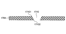
- laser processing is performed on the upper surface of the glass plate 170A having a thickness of 50 ⁇ m to form through holes 171C, respectively.
- a frustum-shaped hole can be formed.
- a truncated cone-shaped through-hole 171C having an opening diameter of the upper end 171C1 of 180 ⁇ m and an opening diameter of the lower end 171C2 of 120 ⁇ m is formed.
- FIG. 4 it is possible to form a through hole 171C having a smaller opening diameter at the end 171C2 than at the end 171C1.
- the end 171C2 positioned on the lower side in FIG. 4 may be such that a slight opening (120 ⁇ m opening here) is formed on the lower surface of the glass plate 170A.
- the size of the truncated cone of the through-hole 171C is set so that the opening diameter of the end 171C1 is 180 ⁇ m and the opening diameter of the end 171C2 is 120 ⁇ m in the next step (FIG. 5). This is because the size does not contact 170A.
- the same processing is performed on the glass plate 170B. Further, an excimer laser, a YAG laser, a UV laser, or an etching process may be used instead of the CO 2 laser.
- the glass plate 170A shown in FIG. 4 is turned upside down (the top and bottom are reversed) and overlaid on the structure 100A as shown in FIG. Further, a glass plate 170B in which a through hole 171D similar to the through hole 171C of the glass plate 170A is formed is superposed under the structure 100A.
- the through-holes 171C and 171D are positioned on the side close to the pads 160A and 160B on the end portions 171C1 and 171D1 having large openings, and the sizes of the through-holes 171C and 171D are the same as those of the pads 160A and 160B and the glass plate. It is set so that 170A and 170B do not contact. For this reason, the glass plates 170A and 170B are not damaged.
- the glass plate 170A, the structure 100A, and the glass plate 170B in a stacked state as shown in FIG. 5 are installed in the press machine 200 as shown in FIG. And heat-sealing.
- the heating temperature is 200 ° C. and the heating time is 90 minutes.
- the insulating layers 110, 120, 130, 140, 150, the wiring layers 121, 131, 141, 151, the lands 121A, 131A, 141A, 151A are thermally fused, and the glass plates 170A, 170B are insulated. It is heat-sealed with the layers 130 and 150.
- the heat bonded structure 100B is taken out from the press machine 200, laser processing is performed from above the through hole 171C, and laser processing is performed from below the through hole 171D. Note that when laser processing is performed from the lower side of the through-hole 171D, the top and bottom of the structure 100B may be reversed.
- the laser processing may be performed to the same depth as the laser processing shown in FIG. 4. By doing so, the through holes 171A and 171B in which the convex portions 171A3 and 171B3 protrude inward can be formed. As shown in FIG. 4, the wiring board 100 can be obtained.
- the wiring substrate 100 in which the glass plates 170A and 170B are provided on the upper surface of the insulating layer 130 and the lower surface of the insulating layer 150, respectively, is obtained.
- the IC chip 190 is formed of silicon or the like, whereas the insulating layers 110, 120, 130, 140, 150 are cores or prepregs, and the insulating layers 110, 120, 130, 140, 150 are more than the IC chip 190. Has a higher coefficient of thermal expansion.
- the wiring board 100 is provided with glass plates 170A and 170B in consideration of the difference in coefficient of thermal expansion between the IC chip 190 and the insulating layers 110, 120, 130, 140, and 150 when the IC chip 190 operates and generates heat. ing.
- the thermal expansion coefficients of the glass plates 170 ⁇ / b> A and 170 ⁇ / b> B are values close to the thermal expansion coefficient of the IC chip 190.
- the glass plates 170 ⁇ / b> A and 170 ⁇ / b> B can suppress the distortion of the insulating layers 110, 120, 130, 140, and 150, and the ICs connected via the solder balls 180
- the connection state between the terminals of the chip 190 and the pads 160A and 160B can be stably maintained.
- the highly reliable wiring board 100 can be provided.
- the glass plate 170A has a flat surface, the distance between the plurality of pads 160A and the plurality of terminals on the lower surface of the IC chip 190 can be made substantially constant. For this reason, the plurality of pads 160A and the plurality of terminals on the lower surface of the IC chip 190 can be reliably connected by the solder balls 180, and the occurrence of poor connection of the solder balls 180 can be suppressed.
- the wiring board 100 can suppress the occurrence of such a situation, the reliability can be improved.
- the end portions 171C1 and 171D1 having large openings of the through holes 171C and 171D are positioned on the side close to the pads 160A and 160B, and the structure 100A and the glass
- the plates 170A and 170B are thermocompression bonded by the press machine 200.
- the sizes of the through holes 171C and 171D are set so that the pads 160A and 160B and the glass plates 170A and 170B do not come into contact with each other. Therefore, even if the thermocompression bonding is performed with the press 200 as shown in FIG. 170B will not be damaged.
- the end portions 171C2 and 171D2 where the openings of the through holes 171C and 171D are small are located on the side far from the pads 160A and 160B. It is possible to prevent the prepreg) from leaking out of the through holes 171C and 171D from the end portions 171C2 and 171D2.
- the prepregs of the insulating layers 130 and 150 enter the through holes 171C and 171D and cover the surfaces of the pads 160A and 160B, the upper side of the through hole 171C and the lower side of the through hole 171D Since the prepreg can be removed when the through holes 171A and 171B are formed by laser processing, the prepreg does not remain on the surfaces of the pads 160A and 160B.
- the insulating layers 130 and 150 are prevented from leaking out of the through holes 171C and 171D, the upper surface of the glass plate 170A and the lower surface of the glass plate 170B are kept flat, and the solder balls 180 Connection failures can be suppressed, and a highly reliable wiring board 100 can be provided.
- the wiring substrate 100 has a through-hole 171A formed so as to avoid the L1 layer pad 160A.
- the diameter of the through hole 171A is set so as to be equal to or larger than the diameter of the pad 160A even in the smallest convex portion 171A3.
- FIG. 8 is a view showing a state in which the solder ball 180 is mounted. Optimizing the size of the solder ball 180 is very important for ensuring the connection between the pad 160A and the terminal of the IC chip 190.
- the surface of the glass plate 170A between the convex portion 171A3 and the upper end 171A1 (the surface above the concave portion 171A3 of the through hole 171A) ) May hold the solder balls 180.
- the insulating layers 110, 120, 130, 140, and 150 may be made of glass.
- the wiring board 100 may include a truncated cone-shaped through hole 171C or 171D without performing the laser processing described with reference to FIG.
- the wiring board 100 may be in a form not including the glass plate 170B when the required strength can be obtained only by the glass plate 170A.
- a solder resist may be applied to the lower surface of the insulating layer 150 instead of the glass plate 170B.
- a structure in which the insulating layers 110, 120, 130, 140, 150, the wiring layers 121, 131, 141, 151, and the lands 121A, 131A, 141A, 151A are heat-sealed is manufactured, and then the glass plates 170A, 170B are manufactured. May be bonded to the insulating layers 130 and 150, respectively.
- the wiring substrate 100 includes the insulating layers 110, 120, 130, 140, 150, the wiring layers 121, 131, 141, 151, the pads 160A, 160B, the glass plates 170A, 170B, and the like, and the L1 layer to the L6.
- a form including layers has been described.
- the wiring board 100 may include an insulating layer 130, a wiring layer 131, lands 131A, vias 132, pads 160A, and a glass plate 170A.
- the insulating layer 130 may be formed of a glass plate and a resin layer. More specifically, a glass plate may be used instead of the insulating layer 130, and a resin layer may be provided so as to cover the wiring layers 121, 131, 141, 151 between the glass plates.
- the wiring board, the electronic device, and the manufacturing method of the wiring board according to the exemplary embodiments of the present invention have been described.
- the present invention is not limited to the specifically disclosed embodiments, Various modifications and changes can be made without departing from the scope of the claims.
Landscapes
- Engineering & Computer Science (AREA)
- Manufacturing & Machinery (AREA)
- Microelectronics & Electronic Packaging (AREA)
- Production Of Multi-Layered Print Wiring Board (AREA)
- Non-Metallic Protective Coatings For Printed Circuits (AREA)
- Structure Of Printed Boards (AREA)
- Physics & Mathematics (AREA)
- Geometry (AREA)
Abstract
信頼性の高い配線基板、電子装置、及び配線基板の製造方法を提供する。 配線基板は、電子部品が実装される第1面と、前記第1面の反対側の第2面とを有する絶縁層と、前記第2面に配設される導電層と、前記絶縁層の前記第1面と前記第2面との間を貫通する貫通孔の内部に設けられるビアと、前記第1面に配設され、前記ビアに接続される電極と、前記第1面に配設され、前記電極を表出させる孔部を有するガラス板とを含む。
Description
本発明は、配線基板、電子装置、及び配線基板の製造方法に関する。
従来より、各々絶縁層と配線パターンよりなる複数のビルドアップ層を積層した樹脂積層体と、前記樹脂積層体の上面および下面に形成された第1および第2のソルダレジスト層と、よりなり、前記第1および第2のソルダレジスト層は、ガラスクロスを含むことを特徴とする多層配線基板がある(例えば、特許文献1参照)。
ところで、配線基板を補強するためにソルダレジスト層にガラスクロスを含ませると、ガラスクロスのある部分とない部分とでソルダレジスト層の表面に凹凸が生じ、配線基板の電極(パッド)と、配線基板の上に実装する電子部品の端子とを接続することが困難になるおそれがある。
このような場合には、配線基板と電子部品とを電気的に接続することができず、信頼性が低下する。
そこで、信頼性の高い配線基板、電子装置、及び配線基板の製造方法を提供することを目的とする。
本発明の実施の形態の配線基板は、電子部品が実装される第1面と、前記第1面の反対側の第2面とを有する絶縁層と、前記第2面に配設される導電層と、前記絶縁層の前記第1面と前記第2面との間を貫通する貫通孔の内部に設けられるビアと、前記第1面に配設され、前記ビアに接続される電極と、前記第1面に配設され、前記電極を表出させる孔部を有するガラス板とを含む。
信頼性の高い配線基板、電子装置、及び配線基板の製造方法を提供することができる。
以下、本発明の配線基板、電子装置、及び配線基板の製造方法を適用した実施の形態について説明する。
<実施の形態>
図1は、実施の形態の配線基板100の断面構造を示す図である。
図1は、実施の形態の配線基板100の断面構造を示す図である。
配線基板100は、絶縁層110、120、130、140、150、配線層121、131、141、151、ランド121A、131A、141A、151A、ビア112、122、132、142、152、パッド160A、160B、ガラス板170A、170Bを含む。
配線基板100は、複数の層を含む多層基板であり、パッド160AのレベルをL1層、配線層131のレベルをL2層、配線層121のレベルをL3層、配線層141のレベルをL4層、配線層151のレベルをL5層、パッド160BのレベルをL6層と称す。すなわち、配線基板100は、6層基板である。
以下では、説明の便宜上、図1における上下関係を用いて、上、又は、下と称す。ただし、これは普遍的な上下関係を示すものではない。また、各構成要素の厚さは、図1における上下方向の厚さを表す。また、平面視とは、図1に断面構造を示す配線基板100を真上、又は、真下から見ることをいう。また、配線基板100の厚さ方向における位置を表す場合に、レベルという文言を用いる。
絶縁層110、120、130、140、150は、例えば、絶縁層130がコアで、絶縁層110、120、140、150がプリプレグである。コアは、絶縁層の一例であり、例えば、ガラス布基材をエポキシ樹脂に含浸させ、両面に銅箔(配線層121、141)を貼り付けたものである。
プリプレグは、絶縁層の一例であり、接着層の一例である。プリプレグとしては、例えば、所謂B-ステージ(半硬化状態)のものが使用される。プリプレグは、例えば、ガラス繊維や炭素繊維等の織布や不織布に、エポキシやポリイミド等の絶縁性樹脂を含浸させたものである。絶縁性樹脂は、熱硬化性樹脂が好適である。
配線層121、131、141、151は、ここでは一例として、L3層、L2層、L4層、L5層の銅箔を所望の配線等の形状にパターニングしたものである。図1に示すように、配線層121、131、141、151は、絶縁層110、120、130、140、150と交互に重ね合わされて、熱圧着される。配線層121、131、141、151は、導電層の一例である。
ランド121A、131A、141A、151Aは、それぞれ、配線層121、131、141、151と同じレベルに位置する。ランド121A、131A、141A、151Aは、それぞれ、配線層121、131、141、151と同様に、L3層、L2層、L4層、L5層の銅箔を円環状にパターニングしたものである。
ランド121A、131A、141A、151Aは、ビア112、122、132、142、152の上又は下に位置し、平面視で、ビア112、122、132、142、152を囲むように配置される。
なお、ここでは一例として、配線層121、131、141、151とランド121A、131A、141A、151Aが銅箔である形態について説明するが、銅(Cu)、ニッケル(Ni)、金(Au)、銀(Ag)、ビスマス(Bi)のいずれかを含む金属であればよい。
ビア112、122、132、142、152は、それぞれ、絶縁層110、120、130、140、150を厚さ方向に貫通する貫通孔(ビアホール)の内部に形成される円柱状の接続部である。絶縁層110、120、130、140、150を厚さ方向に貫通する貫通孔(ビアホール)は、第1貫通孔の一例である。
ビアホールは、例えば、レーザ加工によって形成すればよく、ビア112、122、132、142、152は、めっき処理で形成すればよい。めっき処理で形成する金属(ビア112、122、132、142、152)は、銅(Cu)、ニッケル(Ni)、金(Au)等の金属を用いることができる。
パッド160A、160Bは、それぞれ、ビア132の上端、ビア152の下端に接続するように配設される。パッド160A、160Bは、平面視で円形である。パッド160A、160Bは、配線基板100の上に、IC(Integrated Circuit)チップのような電子部品を実装する際に、はんだボール等を介して、ICチップの下面の端子に接続される。
パッド160A、160Bは、電極の一例である。パッド160A、160Bの直径は、一例として、160μmである。パッド160A、160Bのサイズ(直径)は、プレス機で加熱圧着する際の温度(一例として、200℃)における金属の熱膨張でガラス板170A、170Bと接することがないサイズに設定する。
パッド160A、160Bは、銅(Cu)、ニッケル(Ni)、金(Au)、銀(Ag)、アルミニウム(Al)、チタン(Ti)、錫(Sn)、ビスマス(Bi)のうち1種類以上を含む金属製であればよい。
ガラス板170A、170Bは、それぞれ、配線基板100の上側の表面、下側の表面に配置される。ガラス板170A、170Bは、それぞれ、絶縁層130、150に熱圧着されており、従来の配線基板におけるソルダーレジストの代わりに設けられている。このため、配線基板100は、ソルダーレジストを含まない。
ガラス板170A、170Bは、それぞれ、貫通孔171A、171Bを有する。貫通孔171A、171Bは、平面視で、パッド160A、160Bの位置に合わせて設けられている。貫通孔171A、171Bは、第2貫通孔の一例である。
なお、ガラス板170A、170Bは、酸化アルミニウム(Al2O3)又は二酸化珪素(SiO2)のいずれかを含む材料を用いることが望ましい。また、ガラス板170A、170Bの厚さは、一例として、10μm以上で100μm以下であり、ここでは、50μmであることとする。
貫通孔171Aは、平面視で円形状に開口されている。貫通孔171Aに面するガラス板170Aの内壁は、断面視で、上端171A1及び下端171A2に比べて、上端171A1と下端171A2の間で貫通孔171Aの内側に突出している。
このように貫通孔171Aの内側に突出する部分は、凸部170A3を構築する。すなわち、貫通孔171Aは、凸部170A3を有する。
凸部170A3は、貫通孔171Aの内側にテーパ状に突出しており、平面視で円環状に形成されている。凸部170A3は、貫通孔171Aの内側にテーパ状に突出する円環状のテーパ部である。
凸部171A3を有する貫通孔171Aは、例えば、ガラス板170Aを絶縁層130に重ねる前に、ガラス板170Aの上側及び下側からレーザを照射することによって、形成することができる。
貫通孔171Aの凸部171A3の部分における開口径は、パッド160Aの直径以上である。ここでは、一例として、上端171A1及び下端171A2における貫通孔171Aの開口径が180μmであり、凸部171A3における貫通孔171Aの開口径が160μmである。
上端171A1及び下端171A2における貫通孔171Aの開口径と、凸部171A3における貫通孔171Aの開口径との差は、0μmより大きく、ガラス板170A、170Bの厚さ(ここでは50μm)以下に設定することが望ましい。
貫通孔171Aの凸部171A3の部分における開口径は、パッド160Aの直径以上に設定する。このような凸部171A3を設ける理由については後述する。
貫通孔171Bは、貫通孔171Aと同様の構成を有する。すなわち、貫通孔171Bは、平面視で円形状に開口されている。貫通孔171Bに面するガラス板170Bの内壁には、断面視で、上端171B1及び下端171B2よりも貫通孔171Bの内側に突出する凸部171B3が設けられている。
凸部170B3は、貫通孔171Bの内側にテーパ状に突出しており、平面視で円環状に形成されている。凸部170B3は、貫通孔171Bの内側にテーパ状に突出する円環状のテーパ部である。
凸部171B3を有する貫通孔171Bは、例えば、ガラス板170Bを絶縁層130に重ねる前に、ガラス板170Bの上側及び下側からレーザを照射することによって、形成することができる。
貫通孔171Bの凸部171B3の部分における開口径は、パッド160Bの直径以上である。ここでは、一例として、上端171B1及び下端171B2における貫通孔171Bの開口径が180μmであり、凸部171B3における貫通孔171Bの開口径が160μmである。
上端171B1及び下端171B2における貫通孔171Bの開口径と、凸部171B3における貫通孔171Bの開口径との差は、0μmより大きく、ガラス板170B、170Bの厚さ(ここでは50μm)以下に設定することが望ましい。
貫通孔171Bの凸部171B3の部分における開口径は、パッド160Bの直径以上に設定する。このような凸部171B3を設ける理由については後述する。
図2は、配線基板100にICチップ190を実装した状態を示す図である。図2には、6個のパッド160Aと、2個のパッド160Bとが存在する範囲を示す。このため、説明の便宜上、図1に示す配線基板100の配線層121、131、141、151等の構成を少し変更してあり、配線基板100のL6層には、配線層161が設けられている。
パッド160Aには、はんだボール180を介して、ICチップ190の端子が接続されている。ICチップ190は、所謂フリップチップボンディングの方式で、配線基板100に実装されている。このようなICチップ190の実装は、パッド160Aの上に配置したはんだボール180を、所謂リフロー工程によって溶融させて、ICチップ190の端子と接続させることによって実現される。
はんだボール180は、例えば、銅製のコアボールの周りに、ニッケル、錫等のめっき層を形成したものである。また、ここでは電子部品の一例としてICチップ190を実装する形態について説明するが、ICチップ190の代わりに、メモリチップ、又は、キャパシタ等の電子部品であってもよい。
次に、図3乃至図7を用いて、配線基板100の製造方法について説明する。
図3乃至図7は、配線基板100の製造工程を示す図である。
まず、図3に示すように、熱融着を行っていない状態の絶縁層110、120、130、140、150、配線層121、131、141、151を重ねた構造体100Aを準備する。構造体100Aでは、ランド121A、131A、141A、151A、ビア112、122、132、142、152、パッド160A、160Bが形成されている。
次に、厚さ50μmのガラス板170Aの上面にレーザ加工を行い、それぞれ、貫通孔171Cを形成する。例えば、CO2レーザを用いて加工すると、円錐台状の孔部を形成することができる。この工程では、一例として、上側の端部171C1の開口径が180μm、下側の端部171C2の開口径が120μmの円錐台状の貫通孔171Cを形成する。
このようにすると、図4に示すように、端部171C1よりも端部171C2の方が開口径が小さい貫通孔171Cを形成することができる。図4で下側に位置する端部171C2は、ガラス板170Aの下面に僅かな開口(ここでは120μmの開口)が生じる程度でよい。
貫通孔171Cの円錐台のサイズを端部171C1の開口径が180μmで、端部171C2の開口径が120μmになるように設定するのは、次の工程(図5)において、パッド160Aとガラス板170Aとが接触しないサイズにするためである。
なお、ガラス板170Bについても同様の加工を行う。また、CO2レーザの代わりに、エキシマレーザ、YAGレーザ、UVレーザ、エッチングプロセスを用いてもよい。
次に、図4に示すガラス板170Aを上下を反転させて(天地を逆にして)、図5に示すように、構造体100Aの上に重ねる。また、ガラス板170Aの貫通孔171Cと同様の貫通孔171Dを形成したガラス板170Bを構造体100Aの下に重ね合わせる。
このとき、貫通孔171C、171Dは、開口が大きい端部171C1、171D1側がパッド160A、160Bに近い側に位置しており、かつ、貫通孔171C、171Dのサイズは、パッド160A、160Bとガラス板170A、170Bが接触しないように設定されている。このため、ガラス板170A、170Bが破損することはない。
次に、図5に示すように重ね合わせた状態のガラス板170A、構造体100A、ガラス板170Bを、図6に示すように、プレス機200に設置して、加熱しながら圧力を掛けることにより、熱融着させる。一例として、加熱温度は200℃、加熱時間は90分である。
この工程により、絶縁層110、120、130、140、150、配線層121、131、141、151、ランド121A、131A、141A、151Aが熱融着されるとともに、ガラス板170A、170Bがそれぞれ絶縁層130、150と熱融着される。
次に、熱融着させた構造体100Bをプレス機200から取り出し、貫通孔171Cの上側からレーザ加工を行い、さらに、貫通孔171Dの下側からレーザ加工を行う。なお、貫通孔171Dの下側からレーザ加工を行う場合には、構造体100Bの天地を逆にすればよい。
レーザ加工は、図4に示すレーザ加工と同様の深さまで行えばよく、このようにすることによって、凸部171A3、171B3が内側に突出する貫通孔171A、171Bを形成することができ、図7に示すように、配線基板100を得ることができる。
以上、実施の形態によれば、絶縁層130の上面と、絶縁層150の下面とに、それぞれ、ガラス板170Aと170Bとを設けた配線基板100が得られる。
ICチップ190はシリコン等で形成されるのに対して、絶縁層110、120、130、140、150は、コア又はプリプレグであり、ICチップ190よりも絶縁層110、120、130、140、150の方が熱膨張率が大きい。
配線基板100は、ICチップ190が動作して発熱したときのICチップ190と絶縁層110、120、130、140、150との熱膨張率の違いを考慮して、ガラス板170A、170Bを設けている。ガラス板170A、170Bの熱膨張率は、ICチップ190の熱膨張率にかなり近い値である。
このため、ICチップ190が動作して発熱しても、ガラス板170A、170Bで絶縁層110、120、130、140、150の歪みを抑えることができ、はんだボール180を介して接続されるICチップ190の端子とパッド160A、160Bとの接続状態を安定的に保持することができる。
従って、ガラス板170A、170Bで絶縁層110、120、130、140、150等を補強することにより、信頼性の高い配線基板100を提供することができる。
また、ガラス板170Aは表面が平坦であるため、複数のパッド160Aと、ICチップ190の下面の複数の端子との間隔を略一定にすることができる。このため、複数のパッド160Aと、ICチップ190の下面の複数の端子とをはんだボール180で確実に接続することができ、はんだボール180の接続不良が生じることを抑制できる。
従来の配線基板は、ソルダレジスト層にガラスクロスが混入されているため、ソルダレジスト層の表面に凹凸が生じ、配線基板の複数のパッドと、電子部品の下面の複数の端子とのうち、いずれかのパッドと端子とをはんだボールで接続できなくなるおそれがある。
これに対して、配線基板100は、このような事態が生じることを抑制できるので、信頼性を向上させることができる。
また、配線基板100を製造する工程では、図5に示すように、貫通孔171C、171Dの開口が大きい端部171C1、171D1をパッド160A、160Bに近い側に位置させて、構造体100Aとガラス板170Aと170Bをプレス機200で熱圧着させる。
貫通孔171C、171Dのサイズは、パッド160A、160Bとガラス板170A、170Bが接触しないように設定されているため、図6に示すようにプレス機200で加熱圧着を行っても、ガラス板170A、170Bが破損することはない。
このため、製造工程において、パッド160A、160Bがガラス板170A、170Bに干渉することを抑制でき、ガラス板170A、170Bが割れる、あるいは、欠ける等の破損を抑制することができる。
また、このように熱圧着させる際に、貫通孔171C、171Dの開口が小さい端部171C2、171D2がパッド160A、160Bから遠い側に位置するので、半生状態で固まる前の絶縁層130、150(プリプレグ)が端部171C2、171D2から貫通孔171C、171Dの外に漏れ出ることを抑制することができる。
なお、この工程で、貫通孔171C、171Dの内部に絶縁層130、150のプリプレグが入り込み、パッド160A、160Bの表面を覆ったとしても、貫通孔171Cの上側と貫通孔171Dの下側とをレーザ加工して貫通孔171A、171Bを形成する際にプリプレグを除去できるので、パッド160A、160Bの表面にプリプレグが残ることはない。
絶縁層130、150(プリプレグ)が貫通孔171C、171Dの外に漏れ出ることが抑制されるので、ガラス板170Aの上面とガラス板170Bの下面とが平坦な状態に保たれ、はんだボール180の接続不良を抑制でき、信頼性の高い配線基板100を提供することができる。
また、配線基板100は、L1層のパッド160Aを避けるように形成される貫通孔171Aを有する。貫通孔171Aの直径は、最も小さい凸部171A3の部分においても、パッド160Aの直径以上になるように設定されている。
このため、凸部171A3の開口径と、パッド160Aの直径と、ガラス板170Aの厚さ方向における凸部171A3とパッド160Aとの位置関係を最適化することにより、パッド160Aの上に、適切なサイズのはんだボール180を設置するような空間を確保することができる。
図8は、はんだボール180を実装した状態を示す図である。はんだボール180のサイズを最適化することは、パッド160AとICチップ190の端子との接続を確実なものにする上で、非常に重要である。
例えば、図8に示すように、パッド160Aにはんだボール180の底部が接した状態で、凸部171A3と上端171A1との間のガラス板170Aの面(貫通孔171Aの凹部171A3よりも上側の面)ではんだボール180が保持されるようにしてもよい。
なお、絶縁層110、120、130、140、150は、ガラス製であってもよい。
また、配線基板100は、図7を用いて説明したレーザ加工を行わずに、円錐台状の貫通孔171C、171Dを含む形態であってもよい。
また、配線基板100は、ガラス板170Aだけで必要な強度が得られる場合には、ガラス板170Bを含まない形態であってもよい。この場合には、ガラス板170Bの代わりに、絶縁層150の下面にソルダーレジストを塗布すればよい。
また、絶縁層110、120、130、140、150、配線層121、131、141、151、ランド121A、131A、141A、151Aを熱融着した構造体を作製してから、ガラス板170A、170Bをそれぞれ絶縁層130、150に接着してもよい。
また、以上では、配線基板100が、絶縁層110、120、130、140、150、配線層121、131、141、151、パッド160A、160B、ガラス板170A、170B等を含み、L1層からL6層を含む形態について説明した。
しかしながら、配線基板100は、絶縁層130、配線層131、ランド131A、ビア132、パッド160A、ガラス板170Aを含む形態であってもよい。また、絶縁層130はガラス板と樹脂層で構成してもよい。より具体的には、絶縁層130の代わりにガラス板を用い、ガラス板同士の間で配線層121、131、141、151を覆うように樹脂層を設けてもよい。
以上、本発明の例示的な実施の形態の配線基板、電子装置、及び配線基板の製造方法について説明したが、本発明は、具体的に開示された実施の形態に限定されるものではなく、特許請求の範囲から逸脱することなく、種々の変形や変更が可能である。
本国際出願は2016年3月28日に出願した日本国特許出願2016-063825号に基づく優先権を主張するものであり、日本国特許出願2016-063825号の全内容を本国際出願に援用する。
100 配線基板
110、120、130、140、150 絶縁層
121、131、141、151 配線層
121A、131A、141A、151A ランド
112、122、132、142、152 ビア
160A、160B パッド
170A、170B ガラス板
171A、171B 貫通孔
180 はんだボール
190 ICチップ
200 プレス機
110、120、130、140、150 絶縁層
121、131、141、151 配線層
121A、131A、141A、151A ランド
112、122、132、142、152 ビア
160A、160B パッド
170A、170B ガラス板
171A、171B 貫通孔
180 はんだボール
190 ICチップ
200 プレス機
Claims (7)
- 電子部品が実装される第1面と、前記第1面の反対側の第2面とを有する絶縁層と、
前記第2面に配設される導電層と、
前記絶縁層の前記第1面と前記第2面との間を貫通する第1貫通孔の内部に設けられるビアと、
前記第1面に配設され、前記ビアに接続される電極と、
前記第1面に配設され、前記電極を表出させる第2貫通孔を有するガラス板と
を含む、配線基板。 - 前記電極は、平面視で、前記第2貫通孔の開口よりも小さい、請求項1記載の配線基板。
- 前記第2貫通孔は、前記第1面における第1開口と前記第2面における第2開口との間で、前記第1開口及び前記第2開口よりも開口径が小さくなるように、開口に沿って開口の内側にテーパ状に突出する環状の凸部を有する、請求項1又は2記載の配線基板。
- 前記第2貫通孔は、前記第1面と前記第2面との間で、前記第1面における第1開口が前記第2面における第2開口よりも大きい、又は、前記第1面における第1開口が前記第2面における第2開口よりも小さい、円錐台状の形状を有する、請求項1又は2記載の配線基板。
- 前記絶縁層は、一部にガラス板を用いたものである、請求項1乃至4のいずれか一項記載の配線基板。
- 配線基板と、
前記配線基板に実装される電子部品と
を含む電子装置であって、
前記配線基板が、
電子部品が実装される第1面と、前記第1面の反対側の第2面とを有する絶縁層と、
前記第2面に配設される導電層と、
前記絶縁層の前記第1面と前記第2面との間を貫通する第1貫通孔の内部に設けられるビアと、
前記第1面に配設され、前記ビアに接続される電極と、
前記第1面に配設され、前記電極を表出させる第2貫通孔を有するガラス板と
を有する、電子装置。 - 電子部品が実装される第1面と前記第1面の反対側の第2面とを有する絶縁層に、前記第1面と前記第2面との間を貫通する第1貫通孔の内部に設けられるビアと、前記第1面に配設されて前記ビアに接続される電極とを形成する工程と、
ガラス板に前記電極に対応する第2貫通孔を形成する工程と、
前記絶縁層の前記第1面に、前記第2貫通孔から前記電極が表出するように位置を合わせて、前記ガラス板を重ねる工程と、
前記絶縁層の前記第2面に、導電層を重ねる工程と、
前記絶縁層、前記ガラス板、及び前記導電層を加熱及び加圧して融着させる工程と
を含む、配線基板の製造方法。
Priority Applications (2)
| Application Number | Priority Date | Filing Date | Title |
|---|---|---|---|
| CN201780018829.6A CN108781513B (zh) | 2016-03-28 | 2017-03-24 | 配线基板、电子装置以及配线基板的制造方法 |
| US16/124,730 US10770386B2 (en) | 2016-03-28 | 2018-09-07 | Wiring board, electronic device, and wiring board manufacturing method |
Applications Claiming Priority (2)
| Application Number | Priority Date | Filing Date | Title |
|---|---|---|---|
| JP2016063825A JP6832630B2 (ja) | 2016-03-28 | 2016-03-28 | 配線基板の製造方法 |
| JP2016-063825 | 2016-03-28 |
Related Child Applications (1)
| Application Number | Title | Priority Date | Filing Date |
|---|---|---|---|
| US16/124,730 Continuation US10770386B2 (en) | 2016-03-28 | 2018-09-07 | Wiring board, electronic device, and wiring board manufacturing method |
Publications (1)
| Publication Number | Publication Date |
|---|---|
| WO2017170261A1 true WO2017170261A1 (ja) | 2017-10-05 |
Family
ID=59964594
Family Applications (1)
| Application Number | Title | Priority Date | Filing Date |
|---|---|---|---|
| PCT/JP2017/012127 Ceased WO2017170261A1 (ja) | 2016-03-28 | 2017-03-24 | 配線基板、電子装置、及び配線基板の製造方法 |
Country Status (4)
| Country | Link |
|---|---|
| US (1) | US10770386B2 (ja) |
| JP (1) | JP6832630B2 (ja) |
| CN (1) | CN108781513B (ja) |
| WO (1) | WO2017170261A1 (ja) |
Cited By (1)
| Publication number | Priority date | Publication date | Assignee | Title |
|---|---|---|---|---|
| US20220240378A1 (en) * | 2019-06-13 | 2022-07-28 | Fuji Corporation | Multilayer circuit substrate and method for manufacturing the same |
Families Citing this family (2)
| Publication number | Priority date | Publication date | Assignee | Title |
|---|---|---|---|---|
| EP3588987B1 (en) | 2017-02-24 | 2025-06-18 | JVCKENWOOD Corporation | Filter generation device, filter generation method, and program |
| WO2020241775A1 (ja) | 2019-05-29 | 2020-12-03 | 京セラ株式会社 | 電子素子実装用基板、電子装置、および電子モジュール |
Citations (5)
| Publication number | Priority date | Publication date | Assignee | Title |
|---|---|---|---|---|
| JPH11191670A (ja) * | 1997-12-25 | 1999-07-13 | Victor Co Of Japan Ltd | プリント配線基板及びその製造方法 |
| WO2000010369A1 (en) * | 1998-08-10 | 2000-02-24 | Fujitsu Limited | Method of forming solder bump, method of mounting electronic device, and mounting structure of electronic device |
| JP2000200855A (ja) * | 1999-01-06 | 2000-07-18 | Shinko Electric Ind Co Ltd | Pga型配線基板及びその製造方法並びに半導体装置 |
| JP2005217054A (ja) * | 2004-01-28 | 2005-08-11 | Kyocera Corp | レジスト付き配線基板及び電気装置並びにその製造方法 |
| US20140003009A1 (en) * | 2012-03-07 | 2014-01-02 | Qing Ma | Glass clad microelectronic substrate |
Family Cites Families (9)
| Publication number | Priority date | Publication date | Assignee | Title |
|---|---|---|---|---|
| JPH06283846A (ja) | 1993-03-24 | 1994-10-07 | Ngk Spark Plug Co Ltd | ビア付き配線基板及びその製造方法 |
| JP2003017819A (ja) | 2001-06-29 | 2003-01-17 | Fujitsu Ltd | プリント配線板及びその識別方法 |
| JP5027992B2 (ja) * | 2002-05-23 | 2012-09-19 | ショット アクチエンゲゼルシャフト | 高周波用途のためのガラス材料 |
| KR100512971B1 (ko) | 2003-02-24 | 2005-09-07 | 삼성전자주식회사 | 솔더볼을 이용한 마이크로 전자 기계 시스템의 제조 방법 |
| US7626829B2 (en) * | 2004-10-27 | 2009-12-01 | Ibiden Co., Ltd. | Multilayer printed wiring board and manufacturing method of the multilayer printed wiring board |
| CN100586256C (zh) * | 2005-11-30 | 2010-01-27 | 株式会社村田制作所 | 陶瓷基板、电子器件及陶瓷基板的制造方法 |
| JP4929784B2 (ja) | 2006-03-27 | 2012-05-09 | 富士通株式会社 | 多層配線基板、半導体装置およびソルダレジスト |
| JP2015056561A (ja) * | 2013-09-12 | 2015-03-23 | イビデン株式会社 | プリント配線板及びその製造方法 |
| JP2016058673A (ja) * | 2014-09-12 | 2016-04-21 | イビデン株式会社 | プリント配線板およびその製造方法 |
-
2016
- 2016-03-28 JP JP2016063825A patent/JP6832630B2/ja active Active
-
2017
- 2017-03-24 WO PCT/JP2017/012127 patent/WO2017170261A1/ja not_active Ceased
- 2017-03-24 CN CN201780018829.6A patent/CN108781513B/zh active Active
-
2018
- 2018-09-07 US US16/124,730 patent/US10770386B2/en active Active
Patent Citations (5)
| Publication number | Priority date | Publication date | Assignee | Title |
|---|---|---|---|---|
| JPH11191670A (ja) * | 1997-12-25 | 1999-07-13 | Victor Co Of Japan Ltd | プリント配線基板及びその製造方法 |
| WO2000010369A1 (en) * | 1998-08-10 | 2000-02-24 | Fujitsu Limited | Method of forming solder bump, method of mounting electronic device, and mounting structure of electronic device |
| JP2000200855A (ja) * | 1999-01-06 | 2000-07-18 | Shinko Electric Ind Co Ltd | Pga型配線基板及びその製造方法並びに半導体装置 |
| JP2005217054A (ja) * | 2004-01-28 | 2005-08-11 | Kyocera Corp | レジスト付き配線基板及び電気装置並びにその製造方法 |
| US20140003009A1 (en) * | 2012-03-07 | 2014-01-02 | Qing Ma | Glass clad microelectronic substrate |
Cited By (1)
| Publication number | Priority date | Publication date | Assignee | Title |
|---|---|---|---|---|
| US20220240378A1 (en) * | 2019-06-13 | 2022-07-28 | Fuji Corporation | Multilayer circuit substrate and method for manufacturing the same |
Also Published As
| Publication number | Publication date |
|---|---|
| JP2017183337A (ja) | 2017-10-05 |
| US20190013266A1 (en) | 2019-01-10 |
| CN108781513A (zh) | 2018-11-09 |
| JP6832630B2 (ja) | 2021-02-24 |
| CN108781513B (zh) | 2021-03-12 |
| US10770386B2 (en) | 2020-09-08 |
Similar Documents
| Publication | Publication Date | Title |
|---|---|---|
| JP5395360B2 (ja) | 電子部品内蔵基板の製造方法 | |
| JP2008226945A (ja) | 半導体装置およびその製造方法 | |
| JP6566879B2 (ja) | 電子部品内蔵基板 | |
| JP2016046418A (ja) | 電子部品装置及びその製造方法 | |
| JP2015106615A (ja) | プリント配線板、プリント配線板の製造方法 | |
| JP2017108019A (ja) | 配線基板、半導体パッケージ、半導体装置、配線基板の製造方法及び半導体パッケージの製造方法 | |
| JP2011249759A (ja) | 電子素子内蔵印刷回路基板及びその製造方法 | |
| JP2016063130A (ja) | プリント配線板および半導体パッケージ | |
| TWI506758B (zh) | 層疊封裝結構及其製作方法 | |
| JP2011060875A (ja) | 電子部品内蔵基板及びその製造方法とこれを用いた半導体装置 | |
| US10770386B2 (en) | Wiring board, electronic device, and wiring board manufacturing method | |
| JP6228851B2 (ja) | 配線基板、配線基板の製造方法 | |
| JP4835629B2 (ja) | 半導体装置の製造方法 | |
| JP2008311508A (ja) | 電子部品パッケージおよびその製造方法 | |
| JP2019186330A (ja) | 配線基板、半導体パッケージ及び配線基板の製造方法 | |
| JP2004327743A (ja) | 半田バンプ付き配線基板およびその製造方法 | |
| JP5859678B1 (ja) | プリント配線基板の製造方法 | |
| JP5108253B2 (ja) | 部品実装モジュール | |
| JP2017201674A (ja) | プリント配線板およびその製造方法 | |
| JP2008251869A (ja) | 配線基板およびその製造方法 | |
| JP2008181920A (ja) | 電子部品内蔵基板とこれを用いた電子機器、およびその製造方法 | |
| JP2007059588A (ja) | 配線基板の製造方法および配線基板 | |
| JP5311162B1 (ja) | 部品実装基板の製造方法 | |
| JP2010157628A (ja) | 配線基板およびその製造方法 | |
| JP2005086096A (ja) | 配線基板 |
Legal Events
| Date | Code | Title | Description |
|---|---|---|---|
| NENP | Non-entry into the national phase |
Ref country code: DE |
|
| 121 | Ep: the epo has been informed by wipo that ep was designated in this application |
Ref document number: 17774798 Country of ref document: EP Kind code of ref document: A1 |
|
| 122 | Ep: pct application non-entry in european phase |
Ref document number: 17774798 Country of ref document: EP Kind code of ref document: A1 |