WO2017169804A1 - 異常検知システム及び制御ボード - Google Patents
異常検知システム及び制御ボード Download PDFInfo
- Publication number
- WO2017169804A1 WO2017169804A1 PCT/JP2017/010496 JP2017010496W WO2017169804A1 WO 2017169804 A1 WO2017169804 A1 WO 2017169804A1 JP 2017010496 W JP2017010496 W JP 2017010496W WO 2017169804 A1 WO2017169804 A1 WO 2017169804A1
- Authority
- WO
- WIPO (PCT)
- Prior art keywords
- signal
- abnormality
- controller
- command
- power source
- Prior art date
Links
Images


Classifications
-
- C—CHEMISTRY; METALLURGY
- C23—COATING METALLIC MATERIAL; COATING MATERIAL WITH METALLIC MATERIAL; CHEMICAL SURFACE TREATMENT; DIFFUSION TREATMENT OF METALLIC MATERIAL; COATING BY VACUUM EVAPORATION, BY SPUTTERING, BY ION IMPLANTATION OR BY CHEMICAL VAPOUR DEPOSITION, IN GENERAL; INHIBITING CORROSION OF METALLIC MATERIAL OR INCRUSTATION IN GENERAL
- C23C—COATING METALLIC MATERIAL; COATING MATERIAL WITH METALLIC MATERIAL; SURFACE TREATMENT OF METALLIC MATERIAL BY DIFFUSION INTO THE SURFACE, BY CHEMICAL CONVERSION OR SUBSTITUTION; COATING BY VACUUM EVAPORATION, BY SPUTTERING, BY ION IMPLANTATION OR BY CHEMICAL VAPOUR DEPOSITION, IN GENERAL
- C23C16/00—Chemical coating by decomposition of gaseous compounds, without leaving reaction products of surface material in the coating, i.e. chemical vapour deposition [CVD] processes
- C23C16/44—Chemical coating by decomposition of gaseous compounds, without leaving reaction products of surface material in the coating, i.e. chemical vapour deposition [CVD] processes characterised by the method of coating
- C23C16/52—Controlling or regulating the coating process
-
- C—CHEMISTRY; METALLURGY
- C23—COATING METALLIC MATERIAL; COATING MATERIAL WITH METALLIC MATERIAL; CHEMICAL SURFACE TREATMENT; DIFFUSION TREATMENT OF METALLIC MATERIAL; COATING BY VACUUM EVAPORATION, BY SPUTTERING, BY ION IMPLANTATION OR BY CHEMICAL VAPOUR DEPOSITION, IN GENERAL; INHIBITING CORROSION OF METALLIC MATERIAL OR INCRUSTATION IN GENERAL
- C23C—COATING METALLIC MATERIAL; COATING MATERIAL WITH METALLIC MATERIAL; SURFACE TREATMENT OF METALLIC MATERIAL BY DIFFUSION INTO THE SURFACE, BY CHEMICAL CONVERSION OR SUBSTITUTION; COATING BY VACUUM EVAPORATION, BY SPUTTERING, BY ION IMPLANTATION OR BY CHEMICAL VAPOUR DEPOSITION, IN GENERAL
- C23C16/00—Chemical coating by decomposition of gaseous compounds, without leaving reaction products of surface material in the coating, i.e. chemical vapour deposition [CVD] processes
- C23C16/44—Chemical coating by decomposition of gaseous compounds, without leaving reaction products of surface material in the coating, i.e. chemical vapour deposition [CVD] processes characterised by the method of coating
- C23C16/455—Chemical coating by decomposition of gaseous compounds, without leaving reaction products of surface material in the coating, i.e. chemical vapour deposition [CVD] processes characterised by the method of coating characterised by the method used for introducing gases into reaction chamber or for modifying gas flows in reaction chamber
- C23C16/45523—Pulsed gas flow or change of composition over time
- C23C16/45525—Atomic layer deposition [ALD]
- C23C16/45527—Atomic layer deposition [ALD] characterized by the ALD cycle, e.g. different flows or temperatures during half-reactions, unusual pulsing sequence, use of precursor mixtures or auxiliary reactants or activations
- C23C16/45536—Use of plasma, radiation or electromagnetic fields
-
- C—CHEMISTRY; METALLURGY
- C23—COATING METALLIC MATERIAL; COATING MATERIAL WITH METALLIC MATERIAL; CHEMICAL SURFACE TREATMENT; DIFFUSION TREATMENT OF METALLIC MATERIAL; COATING BY VACUUM EVAPORATION, BY SPUTTERING, BY ION IMPLANTATION OR BY CHEMICAL VAPOUR DEPOSITION, IN GENERAL; INHIBITING CORROSION OF METALLIC MATERIAL OR INCRUSTATION IN GENERAL
- C23C—COATING METALLIC MATERIAL; COATING MATERIAL WITH METALLIC MATERIAL; SURFACE TREATMENT OF METALLIC MATERIAL BY DIFFUSION INTO THE SURFACE, BY CHEMICAL CONVERSION OR SUBSTITUTION; COATING BY VACUUM EVAPORATION, BY SPUTTERING, BY ION IMPLANTATION OR BY CHEMICAL VAPOUR DEPOSITION, IN GENERAL
- C23C16/00—Chemical coating by decomposition of gaseous compounds, without leaving reaction products of surface material in the coating, i.e. chemical vapour deposition [CVD] processes
- C23C16/44—Chemical coating by decomposition of gaseous compounds, without leaving reaction products of surface material in the coating, i.e. chemical vapour deposition [CVD] processes characterised by the method of coating
- C23C16/455—Chemical coating by decomposition of gaseous compounds, without leaving reaction products of surface material in the coating, i.e. chemical vapour deposition [CVD] processes characterised by the method of coating characterised by the method used for introducing gases into reaction chamber or for modifying gas flows in reaction chamber
- C23C16/45523—Pulsed gas flow or change of composition over time
- C23C16/45525—Atomic layer deposition [ALD]
- C23C16/45544—Atomic layer deposition [ALD] characterized by the apparatus
-
- C—CHEMISTRY; METALLURGY
- C23—COATING METALLIC MATERIAL; COATING MATERIAL WITH METALLIC MATERIAL; CHEMICAL SURFACE TREATMENT; DIFFUSION TREATMENT OF METALLIC MATERIAL; COATING BY VACUUM EVAPORATION, BY SPUTTERING, BY ION IMPLANTATION OR BY CHEMICAL VAPOUR DEPOSITION, IN GENERAL; INHIBITING CORROSION OF METALLIC MATERIAL OR INCRUSTATION IN GENERAL
- C23C—COATING METALLIC MATERIAL; COATING MATERIAL WITH METALLIC MATERIAL; SURFACE TREATMENT OF METALLIC MATERIAL BY DIFFUSION INTO THE SURFACE, BY CHEMICAL CONVERSION OR SUBSTITUTION; COATING BY VACUUM EVAPORATION, BY SPUTTERING, BY ION IMPLANTATION OR BY CHEMICAL VAPOUR DEPOSITION, IN GENERAL
- C23C16/00—Chemical coating by decomposition of gaseous compounds, without leaving reaction products of surface material in the coating, i.e. chemical vapour deposition [CVD] processes
- C23C16/44—Chemical coating by decomposition of gaseous compounds, without leaving reaction products of surface material in the coating, i.e. chemical vapour deposition [CVD] processes characterised by the method of coating
- C23C16/50—Chemical coating by decomposition of gaseous compounds, without leaving reaction products of surface material in the coating, i.e. chemical vapour deposition [CVD] processes characterised by the method of coating using electric discharges
- C23C16/515—Chemical coating by decomposition of gaseous compounds, without leaving reaction products of surface material in the coating, i.e. chemical vapour deposition [CVD] processes characterised by the method of coating using electric discharges using pulsed discharges
-
- G—PHYSICS
- G05—CONTROLLING; REGULATING
- G05B—CONTROL OR REGULATING SYSTEMS IN GENERAL; FUNCTIONAL ELEMENTS OF SUCH SYSTEMS; MONITORING OR TESTING ARRANGEMENTS FOR SUCH SYSTEMS OR ELEMENTS
- G05B19/00—Programme-control systems
- G05B19/02—Programme-control systems electric
- G05B19/04—Programme control other than numerical control, i.e. in sequence controllers or logic controllers
- G05B19/048—Monitoring; Safety
-
- G—PHYSICS
- G05—CONTROLLING; REGULATING
- G05B—CONTROL OR REGULATING SYSTEMS IN GENERAL; FUNCTIONAL ELEMENTS OF SUCH SYSTEMS; MONITORING OR TESTING ARRANGEMENTS FOR SUCH SYSTEMS OR ELEMENTS
- G05B23/00—Testing or monitoring of control systems or parts thereof
- G05B23/02—Electric testing or monitoring
- G05B23/0205—Electric testing or monitoring by means of a monitoring system capable of detecting and responding to faults
- G05B23/0218—Electric testing or monitoring by means of a monitoring system capable of detecting and responding to faults characterised by the fault detection method dealing with either existing or incipient faults
- G05B23/0221—Preprocessing measurements, e.g. data collection rate adjustment; Standardization of measurements; Time series or signal analysis, e.g. frequency analysis or wavelets; Trustworthiness of measurements; Indexes therefor; Measurements using easily measured parameters to estimate parameters difficult to measure; Virtual sensor creation; De-noising; Sensor fusion; Unconventional preprocessing inherently present in specific fault detection methods like PCA-based methods
-
- G—PHYSICS
- G05—CONTROLLING; REGULATING
- G05B—CONTROL OR REGULATING SYSTEMS IN GENERAL; FUNCTIONAL ELEMENTS OF SUCH SYSTEMS; MONITORING OR TESTING ARRANGEMENTS FOR SUCH SYSTEMS OR ELEMENTS
- G05B23/00—Testing or monitoring of control systems or parts thereof
- G05B23/02—Electric testing or monitoring
- G05B23/0205—Electric testing or monitoring by means of a monitoring system capable of detecting and responding to faults
- G05B23/0259—Electric testing or monitoring by means of a monitoring system capable of detecting and responding to faults characterized by the response to fault detection
- G05B23/0264—Control of logging system, e.g. decision on which data to store; time-stamping measurements
-
- H—ELECTRICITY
- H01—ELECTRIC ELEMENTS
- H01L—SEMICONDUCTOR DEVICES NOT COVERED BY CLASS H10
- H01L21/00—Processes or apparatus adapted for the manufacture or treatment of semiconductor or solid state devices or of parts thereof
- H01L21/67—Apparatus specially adapted for handling semiconductor or electric solid state devices during manufacture or treatment thereof; Apparatus specially adapted for handling wafers during manufacture or treatment of semiconductor or electric solid state devices or components ; Apparatus not specifically provided for elsewhere
- H01L21/67005—Apparatus not specifically provided for elsewhere
- H01L21/67242—Apparatus for monitoring, sorting or marking
- H01L21/67253—Process monitoring, e.g. flow or thickness monitoring
-
- G—PHYSICS
- G05—CONTROLLING; REGULATING
- G05B—CONTROL OR REGULATING SYSTEMS IN GENERAL; FUNCTIONAL ELEMENTS OF SUCH SYSTEMS; MONITORING OR TESTING ARRANGEMENTS FOR SUCH SYSTEMS OR ELEMENTS
- G05B2219/00—Program-control systems
- G05B2219/30—Nc systems
- G05B2219/45—Nc applications
- G05B2219/45026—Circuit board, pcb
Definitions
- the present invention relates to an abnormality detection system and a control board.
- Patent Document 1 discloses a plurality of command signals for instructing opening / closing operations of a plurality of valves provided in a plasma apparatus, and a plurality of detection signals of a plurality of sensors for detecting opening / closing operations of a plurality of valves.
- a control controller for grasping the operation state of the valve is disclosed.
- a controller that controls the plasma CVD apparatus detects a status signal of a high-frequency power supply (hereinafter also referred to as “RF power supply”) or a valve attached to the plasma CVD apparatus in a cycle of 100 ms. To do. That is, the control controller polls the sensor and the RF power source at a cycle of 100 ms.
- RF power supply high-frequency power supply
- plasma control is performed in units of 10 ms. It is done in the cycle.
- the IO (Input / Output) signal of the sensor or RF power supply is controlled at a period of the conventional 100 ms unit, the state of the device such as a valve provided in the plasma ALD apparatus is accurately grasped, and the process control is appropriately performed. It can be difficult to do.
- the present invention is directed to accurately detecting the state of an apparatus provided in a substrate processing apparatus.
- a first controller that controls the substrate processing apparatus and a second controller that controls equipment provided in the substrate processing apparatus in accordance with an instruction from the first controller.
- An abnormality detection system for detecting an abnormality of the device, wherein the second controller collects the state signal of the device at a predetermined sampling period and a predetermined sampling interval,
- a storage unit configured to store the collected status signal of the device, wherein the first controller acquires the acquired status signal of the device from the second controller at a time interval equal to or greater than the predetermined time;
- An abnormality detection system is provided that includes an abnormality determination unit that determines whether there is an abnormality in the device based on the state signal of the device.
- the state of equipment provided in the substrate processing apparatus can be detected with high accuracy.
- the flowchart which shows an example of the abnormality detection process which concerns on 1st Embodiment.
- the figure for demonstrating the timing of the status signal (digital, analog signal) which concerns on 1st-6th embodiment The flowchart which shows an example of the abnormality detection process which concerns on 2nd Embodiment. The time chart of each signal in the abnormality detection process which concerns on 2nd Embodiment. The figure which shows an example of the state signal detection circuit which concerns on 3rd Embodiment. The time chart of each signal in the abnormality detection process which concerns on 3rd Embodiment. The figure which shows an example of the state signal detection circuit which concerns on 4th Embodiment. The time chart of each signal in the abnormality detection process which concerns on 4th Embodiment. The figure which shows an example of the state signal detection circuit which concerns on 5th Embodiment.
- the time chart of each signal in the abnormality detection process which concerns on 5th Embodiment The figure for demonstrating the integration method in the abnormality detection process which concerns on 5th Embodiment.
- a substrate processing system includes a plurality of substrate processing apparatuses, a transfer chamber (TM), a load lock chamber (LLM), and the like, and a plurality of substrate processing apparatuses can process a plurality of substrates.
- TM transfer chamber
- LLM load lock chamber
- a system controller 1 EC: Equipment Controller
- EC Equipment Controller
- the system controller 1 is connected to a plurality of module controllers 20 (MC: Module Controller) via a network 2 such as an in-system LAN (Local Area Network).
- MC Module Controller
- the module controller 20 controls the substrate processing apparatus in accordance with instructions from the system controller 1.
- Each module controller 20 is connected to a plurality of I / O boards 30 via a network 2 such as an in-system LAN (Local Area Network).
- the plurality of I / O boards 30 controls at least one of the plurality of devices provided in the substrate processing apparatus in accordance with instructions from each module controller 20.
- one I / O board 30 among the plurality of I / O boards 30 controls each device such as an RF power source 18 and a matching unit 17 as an example of a high frequency power source, as shown in FIGS. 1 and 2. .
- the I / O board 30 sends a command signal for turning on the RF (hereinafter referred to as “DO (Digital Output) signal”) in accordance with a command from the module controller (MC) 20. To send. Further, the I / O board 30 inputs a confirmation signal for the DO signal (hereinafter referred to as “DI (Digital Input) signal”) from the RF power source 18.
- DO Digital Output
- DI Digital Input
- the system controller (EC) 1 is expressed as EC1
- the module controller (MC) 20 is expressed as MC20.
- the MC 20 is an upper controller for the I / O board 30, and the I / O board 30 is a lower controller for the MC 20.
- the I / O board 30 is also called a control boat.
- the upper controller is an example of a first controller
- the lower controller is an example of a second controller.
- the substrate processing apparatus 10 may be an apparatus such as a plasma CVD apparatus, a plasma ALD apparatus, or a plasma etching apparatus.
- the substrate processing apparatus 10 intermittently repeatedly supplies a plurality of gases to semiconductor wafers (hereinafter simply referred to as “wafers”) W, which is an example of a substrate, at different timings. It is configured as an ALD (Atomic Layer Deposition) apparatus for film formation.
- ALD Atomic Layer Deposition
- the substrate processing apparatus 10 is connected to the processing container 11 via a processing container 11, a gas supply source 14 for supplying a plurality of gases used for processing the wafer W, and a matching unit 17.
- An RF power source 18 for applying (high frequency) power and an exhaust device 16 are provided.
- the processing container 11 includes a top wall 11a, a bottom wall 11b, and a side wall 11c that connects the top wall 11a and the bottom wall 11b, is formed in a substantially cylindrical shape, and the inside thereof is airtight.
- An exhaust port 11d is formed in the bottom wall 11b.
- the EC 1 reads a program including a recipe designated by a process manager or the like from a hard disk device or a storage medium. The read program is transmitted from the EC 1 to each MC 20.
- the EC 1 is connected via a network 2 such as a LAN to a host computer as a MES (Manufacturing Execution System) that manages the manufacturing process of the entire factory where the substrate processing system is installed.
- the host computer feeds back real-time information about various processes in the factory to the core business system, and controls the processes in consideration of the load of the entire factory.
- MES Manufacturing Execution System
- Recipes relating to overall control of the substrate processing system, abnormality detection of the substrate processing apparatus 10 and processing of the wafer W are stored in, for example, a storage medium and can be used by being installed in a hard disk device.
- a storage medium for example, a CD-ROM, a hard disk, a flexible disk, a flash memory, a DVD, or the like can be used.
- the recipe can also be transmitted online from another device, for example, via a dedicated line and used online.
- the plurality of MCs 20 are controlled and controlled by EC1.
- the MC 20 can be provided corresponding to not only a plurality of substrate processing apparatuses 10 in the substrate processing system but also a load lock chamber and a loader unit. In this case, the MC 20 is controlled and controlled by the EC 1. .
- the MC 20 includes a volatile memory 23 configured by an I / O control interface 21, a CPU 22, a RAM, and the like, and a nonvolatile memory 24 configured by a ROM or the like.
- the nonvolatile memory 24 includes, for example, a nonvolatile memory such as an SRAM (Static Random Access Memory), an MRAM (Magnetoresistive Random Access Memory), an EEPROM (Electrically Erasable Programmable Read-Only Memory), and a flash memory.
- the non-volatile memory 24 stores various log information in the substrate processing apparatus 10, for example, a status signal log when an abnormality of the substrate processing apparatus 10 is determined.
- Information stored in the nonvolatile memory 24 as a status signal includes various signals input / output between the MC 20 and the I / O board 30, such as a DO (Digital Output) signal, a DI (Digital Input) signal, and an AO. (Analog output) signal, AI (analog input) signal, and the like.
- the MC 20 is connected to one or more I / O modules 31 via the network 48.
- the network 48 has a plurality of channels CH0, CH1, CH2,... Assigned to each I / O module 31.
- the network 48 may be a network realized by using an LSI called GHOST (General High-Speed Optimum Scalable Transceiver).
- Control of each device provided in the substrate processing apparatus 10 by the MC 20 is performed via the I / O module 31.
- the I / O control interface 21 of the MC 20 sends various control signals to the I / O module 31.
- the I / O control interface 21 receives status signals of devices (for example, the RF power supply 18 and the matching unit 17) from the I / O module 31.
- I / O board One or more I / O modules 31 corresponding to the MC 20 transmit input / output signals of control signals to the substrate processing apparatus 10.
- One I / O module 31 has one or more I / O boards 30.
- the I / O board 30 is a control board that directly controls each device in accordance with instructions from the MC 20.
- the function of the I / O board 30 is realized using, for example, at least one of a CPU 32 and an FPGA (Field Programmable Gate Array) circuit 34 as main components.
- the FPGA circuit 34 is an example of a programmable logic device.
- the I / O module 31 is connected to one or more devices.
- the RF power source 18 and the matching unit 17 are connected to one I / O board 30.
- Control of output signals (for example, DO signal and AO signal) output from the MC 20 (I / O board 30) to the device and input signals (for example, DI signal and AI signal) input to the I / O board 30 are as follows. It is executed by the CPU 32 and the FPGA 34.
- the DO signal is a digital signal output from the MC 20 positioned above the control system to the RF power source 18 positioned below the control system.
- the DO signal includes a signal that commands turning on the RF power supply 18.
- the DO signal includes a signal for commanding the RF power supply 18 to be turned off.
- the DI signal is a digital signal that is input from the RF power source 18 positioned at the lower level of the control system to the MC 20 (I / O board 30) positioned at the higher level of the control system.
- the DI signal includes a confirmation signal for a command signal that commands turning on the RF power supply 18.
- the DI signal includes a confirmation signal for a command signal for commanding the RF power supply 18 to be turned off.
- the DO counter 40 built in the FPGA circuit 34 counts the number of rising or falling of the command signal.
- the DI counter 41 built in the FPGA circuit 34 counts the number of rising or falling edges of the confirmation signal with respect to the command signal.
- the rise delay time counter 45 incorporated in the FPGA circuit 34 is a DO signal (actually, a DI signal input by feeding back the DO signal) that is a command signal for commanding the RF power source 18 to be turned on, and the RF power source 18.
- the relative time difference between the DI signal, which is a confirmation signal with respect to the command signal for commanding ON, is measured.
- the fall delay time counter 46 built in the FPGA circuit 34 includes a DO signal (actually, a DI signal input by feeding back the DO signal) as a command signal for commanding the RF power supply 18 to be turned off, and an RF power supply.
- the relative time difference between the DI signal which is the confirmation signal with respect to the command signal for instructing 18 to be turned off is measured.
- the AI signal is an analog signal input from the RF power source 18 and the matching unit 17 to the MC 20 (I / O board 30), for example.
- the AI signal includes a signal (hereinafter referred to as “Pf AI signal”) indicating a traveling wave power Pf of a high frequency (RF) supplied from the RF power source 18. Further, the AI signal includes a signal (hereinafter referred to as “Pr AI signal”) indicating the power Pr of the high frequency (RF) reflected wave supplied from the RF power source 18.
- the AI signal includes a signal indicating a high-frequency (RF) traveling wave voltage Vpp supplied from the RF power source 18 (hereinafter referred to as “Vpp AI signal”).
- Vpp AI signal includes a signal indicating the matching position of the variable capacitor provided in the matching unit 17 (hereinafter referred to as “Load AI signal”, “Tune AI signal”).
- the maximum value register 42 built in the CPU 32 the maximum value of the Pf AI signal (analog signal of RF traveling wave power Pf), the maximum value of the Pr AI signal (analog signal of RF reflected wave power Pr), Vpp AI The maximum value of the signal (analog signal of the RF traveling wave voltage Vpp) and the maximum value of the Load AI signal and the Tune AI signal (signal indicating the maximum value of the matching position of the matching unit 17) are stored.
- the minimum value register 43 built in the CPU 32 the minimum value of the Pf AI signal (analog signal of RF traveling wave power Pf), the minimum value of the Pr AI signal (analog signal of RF reflected wave power Pr), Vpp AI The minimum value of the signal (analog signal of the RF traveling wave voltage Vpp) and the minimum value of the Load AI signal and the Tune AI signal (the signal indicating the minimum value of the matching position of the matching unit 17) are stored.
- the integration register 44 built in the CPU 32 has an integration value of the Pf AI signal (analog signal of RF traveling wave power Pf) and an integration value of the Pr AI signal (analog signal of RF reflected wave power Pr). Stored.
- the various analog signals in the first to sixth embodiments described below mean signals obtained by digitizing signals having properties represented by analog values.
- the I / O board 30 includes a communication unit 36, a storage unit 37, a time measuring unit 38, and a device control unit 39.
- the communication unit 36 receives a command signal for turning on the RF power source 18 from the MC 20 and transmits a DO signal to the RF power source 18 in accordance with the command signal.
- the communication unit 36 transmits a confirmation signal (DI signal) for the command signal (DO signal) to the MC 20.
- the communication unit 36 transmits to the MC 20 an AI signal related to the high frequency of the RF power supply 18 and an AI signal related to the matching position of the matching unit 17.
- the device control unit 39 collects device status signals at a predetermined sampling interval for a predetermined period and accumulates the collected device status signals in the storage unit 37. Specifically, the device control unit 39 outputs the number of command signals to the RF power source 18 provided in the substrate processing apparatus 10 via the communication unit 36, the number of confirmation signals corresponding to the command signals, and the RF power source 18 outputs.
- the storage unit 37 stores, in the DO counter 40 and the DI counter 41, the number of DO signals that command the turning on of the RF power supply 18 and the number of DI signals that are confirmation signals for the DO signals.
- the storage unit 37 stores the maximum values of the various AI signals in the maximum value register 42 and stores the minimum values of the various AI signals in the minimum value register 43.
- the storage unit 37 stores the accumulated value of the AI signal of the RF traveling wave and the RF reflected wave in the integration register 44.
- the storage unit 37 stores, in the rise delay time counter 45, the difference between the rise of the DO signal that commands turning on the RF power supply 18 and the rise of the DI signal that is the confirmation signal as a delay time.
- the storage unit 37 stores, in the fall delay time counter 46, the difference between the fall of the DO signal that commands turning on the RF power supply 18 and the fall of the DI signal that is the confirmation signal as a delay time.
- the timer 38 measures a predetermined cycle when collecting the state signal of the device, a predetermined time for sampling in the cycle, and a sampling interval.
- the I / O board 30 polls the RF power source 18 and the matching unit 17 at a sampling interval determined in a range of 300 ⁇ s to 1 ms, and collects status signals of the RF power source 18 and the matching unit 17. .
- the substrate processing apparatus 10 is a plasma ALD apparatus, one process is performed at a cycle of 200 ms to 800 ms. Therefore, the timer 38 measures a predetermined sampling time every 200 ms to 800 ms (that is, every process). For example, in FIG. 8, the sampling time of the predetermined time is 50 ms to 100 ms.
- the sampling time is a predetermined time (between 50 ms and 100 ms) and 300 ⁇ s.
- Polling is performed from the I / O board 30 to the RF power source 18 and the matching unit 17 at a sampling interval determined in a range of ⁇ 1 ms.
- the I / O board 30 collects the status signals of the RF power source 18 and the matching unit 17 as sampling data.
- the collected sampling data of the device status signal is stored in the storage unit 37.
- the storage unit 37 is realized by the RAM 33 in the CPU 32 and the various counters 40 and 41 and the various registers 42 to 44 in the FPGA circuit 34 shown in FIG.
- the sampling interval is set to 300 ⁇ s, but the sampling interval is not limited to this and can be set as appropriate.
- Sampling data is sent from the I / O board 30 to the MC 20 at the polling timing sent by the MC 20 every 100 ms.
- the equipment control unit 39 controls equipment provided in the substrate processing apparatus 10. Specifically, the device control unit 39 performs on / off control of the RF power source 18, exhaust control of the exhaust device 16, gas supply control of the gas supply source 14, and the like. In addition, the device control unit 39 performs control such as stopping of the corresponding device according to the determination result of the abnormality of the devices such as the RF power supply 18 and the matching unit 17.
- the MC 20 includes a communication unit 25, a control unit 26, an abnormality determination unit 27, and a log storage unit 28.
- the communication unit 25 transmits and receives various signals such as a DO signal, a DI signal, and an AI signal to and from the I / O board 30.
- the control unit 26 controls the substrate processing apparatus 10 according to the instruction of EC1.
- the abnormality determination unit 27 calculates the peak value and average of sampling data of the state signal (for example, Pf AI signal) of the RF power source 18 and the state signal (for example, Load / Tune AI signal) of the matcher 17 collected in the I / O board 30. Based on the value and the median value, it is determined whether there is an abnormality in devices such as the RF power source 18 and the matching unit 17. More specifically, the abnormality determination unit 27 may determine whether there is an abnormality in the device or an abnormality in the wiring between the devices based on at least one of the following signals based on the state signal of the device.
- the state signal for example, Pf AI signal
- the state signal for example, Load / Tune AI signal
- the status signal of the device determined to be abnormal is stored as log information.
- a plasma control period (time for one process) of a CVD apparatus that performs a film forming process by a CVD method is sufficient if it is about 100 ms.
- the plasma control period of the ALD apparatus that performs the film forming process by the ALD method needs to be set as short as about 10 ms because the on / off period of the RF power source 18 is shortened. Therefore, in the polling performed by the MC 20 every 100 ms, the MC 20 may not always correctly acquire the status signal of the device such as the RF power source 18 that is plasma-controlled with a short period of about 10 ms.
- the device status signal is accumulated in the storage unit 37 in the I / O board 30 by polling performed by the I / O board 30 every 300 ⁇ s to 1 ms.
- the MC 20 acquires the status signal of the device accumulated in the storage unit 37 in the I / O board 30 at the polling performed every 100 ms, so that the status signal of the device such as the RF power supply 18 is sent to the I / O board 30. Can be obtained correctly.
- the MC 20 can accurately determine the state (the presence / absence of abnormality) of devices such as the RF power supply 18 based on the acquired device state signal even in an ALD apparatus that is plasma-controlled with a short period of about 10 ms. it can.
- FIG. 4 shows an example of a state signal detection circuit according to the first embodiment.
- FIG. 5 is a flowchart illustrating an example of the abnormality detection process according to the first embodiment.
- FIG. 6 is a time chart of each signal in the abnormality detection process according to the first embodiment.
- the state signal detection circuit 35 is in the FPGA circuit 34, and includes a photocoupler 50, a DO counter 40, and a DI counter 41.
- the photocoupler 50 is an element that transmits a signal while being electrically insulated by internally converting the electrical signal into light and returning it to the electrical signal.
- the DO counter 40 counts the number of signals (DO signal) obtained by feeding back a command signal for controlling the turning on of the RF power source 18 from the MC 20 through the photocoupler 50.
- the DI counter 41 counts the number of confirmation signals (DI signals) with respect to the DO signal that controls turning on of the RF power source 18 from the MC 20.
- the DO counter 40 and the DI counter 41 are each 16 bits, and, as shown in FIG. 6, start counting according to the START command controlled by the MC software (program) installed in the MC 20, and stop counting according to the STOP command. To do.
- the DO counter 40 and the DI counter 41 count rising edges of the DO signal and DI signal, but the present invention is not limited to this, and the falling edges of the DO signal and DI signal may be counted.
- the DO counter 40 and DI counter 41 are initialized by a RESET command.
- the counter values of the DO counter 40 and DI counter 41 can be read even during counting.
- a signal noise removal circuit is provided in front of the DI counter 41 so that a DI signal that does not have a signal level continuing for a certain time or longer is not determined as a valid signal.
- the abnormality detection process according to the first embodiment shown in FIG.
- the DO counter 40 counts the number A of RF ON DO signals
- the DI counter 41 counts the number B of RF ON DI signals.
- the DO counter 40 stops counting the number A of RF ON DO signals
- the DI counter 41 stops counting the number B of RF ON DI signals.
- the DO counter 40 and the DI counter 41 are initialized according to the RESET signal at time tr.
- the control unit 26 counts the number of output times X of the DO signal instructing to turn on the RF power supply 18 (step S10).
- the communication unit 25 acquires the count number A stored in the DO counter 40 and the count number B stored in the DI counter 41 from the communication unit 36 of the I / O board 30 (step S12).
- the abnormality determination unit 27 determines whether the output count X is equal to the count number A (step S14). If the abnormality determination unit 27 determines that the output count X is not equal to the count number A, it determines that there is an abnormality in the I / O board 30 (step S16), and ends this process. On the other hand, when determining that the output count X is equal to the count number A, the abnormality determination unit 27 determines whether the output count X is equal to the count number B (step S18).
- the abnormality determination unit 27 determines that the output count X is equal to the count number B, it determines that there is no abnormality (step S20), and ends this process. On the other hand, if the abnormality determination unit 27 determines that the output count X is not equal to the count number B, it determines that there is an abnormality in the wiring between the I / O board 30 and the RF power supply 18 or the RF power supply 18 (step S22), the process ends.
- the abnormality of the wiring between the RF power source 18 and the I / O board 30 and the RF power source 18 and the I / O board 30 provided in the substrate processing apparatus 10. Can be detected.
- FIG. 7 shows an example of a state signal detection circuit according to the second embodiment.
- FIG. 8 is a time chart for explaining state signals (DO, DI, AI signals) according to the first to sixth embodiments.
- FIG. 9 is a flowchart showing an example of the abnormality detection process according to the second to fifth embodiments.
- FIG. 10 is a time chart for explaining an example of the abnormality detection process according to the second embodiment.
- the state signal detection circuit 35 is in the FPGA circuit 34 and includes an AI circuit 51, a maximum value register 42, and a minimum value register 43.
- the AI circuit 51 outputs a Pf AI signal obtained by digitizing an analog signal of RF traveling wave power Pf into 12-bit data. Also, a Pr AI signal obtained by digitizing an analog signal of RF reflected wave power Pr into 12-bit data is output.
- a START command signal is output at time t3, a STOP command signal is output at time t4, and a RESET signal is output at time tr.
- data is sampled every sampling clock of 300 ⁇ s.
- the sampling time is a predetermined time in a range of 50 ms to 100 ms in one process.
- the maximum value of the Pf AI signal and the maximum value of the Pr AI signal are stored in the maximum value register 42, respectively.
- the minimum value of the Pf AI signal and the minimum value of the Pr AI signal are stored in the minimum value register 43, respectively.
- the maximum value register 42 and the minimum value register 43 each have 12 bits, and detection of the maximum value and minimum value is started by the START command controlled by the MC software of the MC 20, and the detection is stopped by the STOP command.
- the maximum value register 42 and the minimum value register 43 are initialized by a RESET command.
- the substrate processing apparatus 10 is a plasma ALD apparatus
- one process is performed in 200 ms to 800 ms. Therefore, as shown in FIG. 8, the interval between the START command (t0, t3,%) And the STOP command (t2, t4,%) Of the Pf AI signal is 200 ms to 800 ms. Therefore, sampling data is collected once for each process of 200 ms to 800 ms.
- Sampling data is collected at a sampling interval of 300 ⁇ s to 1 ms within a predetermined time in the range of 50 ms to 100 ms. For example, sampling data of a plurality of Pf AI signals and Pr AI signals are collected every 300 ⁇ s within a predetermined time of 50 ms. The collected sampling data of the Pf AI signal and the Pr AI signal are stored in the storage unit 37 of the I / O board 30.
- the START command (t0) to the STOP command (t1) in the first embodiment includes about 300 processes, the START command (t0, t3,... In the second embodiment is included. ⁇ ) To the STOP command (t2, t4,...) Is longer than the time.
- the MC20 polls every 100 ms, for example.
- the period at which the MC 20 acquires the sampling data of the AI signal is longer than or equal to a predetermined time 50 ms to 100 ms in one cycle 200 to 800 ms of processing by the ALD method, for example. Therefore, the sampling data of the AI signal acquired by the MC 20 by one polling of the MC 20 is the sampling data of the AI signal for one time, and the sampling data of the AI signal for a plurality of times is acquired by one polling. There is no.
- the abnormality detection process according to the second embodiment shown in FIG. 9 is executed by the MC 20.
- the control unit 26 synchronizes with the polling timing, and the Pf (RF of the sampling data) collected at a predetermined sampling interval (300 ⁇ s in this embodiment) via the communication unit 25.
- the maximum value and minimum value of the AI signal of traveling wave power) and the maximum value and minimum value of the AI signal of Pr (reflected wave power of RF) are received from the I / O board 30 (step S32).
- the abnormality determination unit 27 determines whether or not the maximum value of the Pf AI signal is larger than a predetermined threshold A (step S34). If the abnormality determining unit 27 determines that the maximum value of the Pf AI signal is greater than the predetermined threshold A, the abnormality determining unit 27 determines that the RF power source 18 is abnormal (step S36), and ends the process. On the other hand, when it is determined that the maximum value of the Pf AI signal is equal to or less than the predetermined threshold A, the abnormality determination unit 27 determines whether or not the minimum value of the Pf AI signal is smaller than the predetermined threshold B ( Step S38).
- the abnormality determination unit 27 determines that the RF power source 18 is abnormal (step S36), and ends the present process.
- the abnormality determination unit 27 determines whether the maximum value of the Pr AI signal is greater than the predetermined threshold C (Ste S40). If the abnormality determination unit 27 determines that the maximum value of the Pr AI signal is greater than the predetermined threshold C, the abnormality determination unit 27 determines that the RF power source 18 is abnormal (step S36), and ends the process.
- the abnormality determination unit 27 determines whether the minimum value of the Pr AI signal is smaller than the predetermined threshold D (Ste S42).
- the abnormality determination unit 27 determines that the RF power source 18 is abnormal (step S36), and ends the present process. On the other hand, if the abnormality determination unit 27 determines that the minimum value of the Pr AI signal is equal to or greater than the predetermined threshold D, the abnormality determination unit 27 determines that there is no abnormality in the device (step S44), and ends the present process.
- the maximum value and the minimum value in the range of ⁇ 5% of the central value of the AI signal of Pf when a normal process is performed are set as the threshold value A and the threshold value B, respectively. It may be set.
- the maximum value and the minimum value in the range of ⁇ 5% of the center value of the Pr AI signal when a normal process is performed may be set as the threshold value C and the threshold value D, respectively.
- the setting of each threshold value A to D is not limited to this, and other allowable values indicating a range that does not deviate from a normal process can be used.
- the I / O board 30 samples the sampling data of the Pf AI signal and the Pr AI signal at a time equal to or shorter than the polling cycle of the MC 20, for example, 300 ⁇ s. Collected at intervals and stored in the storage unit 37. As a result, the collected sampling data is temporarily stored in the I / O board 30.
- the MC 20 acquires the sampling data from the I / O board 30 at the polling period, so that the abnormality of the RF power source 18 can be accurately detected based on the accumulated sampling data.
- the MC 20 determines whether there is an abnormality in the device such as the RF power source 18 based on the maximum and minimum values of the Pf AI signal and the maximum and minimum values of the Pr AI signal. Not exclusively.
- the MC 20 may calculate a peak value, an average value, a median value, and the like of the sampling data acquired from the I / O board 30 every polling, and determine whether there is an abnormality in the device based on the calculation result.
- FIG. 11 shows an example of a state signal detection circuit according to the third embodiment.
- FIG. 12 is a time chart of each signal in the abnormality detection process according to the third embodiment.
- a state signal detection circuit 35 according to the third embodiment shown in FIG. 11 is in the FPGA circuit 34 and includes an AI circuit 51, a maximum value register 42, and a minimum value register 43.
- the AI circuit 51 outputs a Vpp AI signal obtained by digitizing an analog signal of the RF traveling wave voltage Vpp into 12-bit data.
- the maximum value register 42 and the minimum value register 43 each have 12 bits, start detection of the maximum and minimum values of the Vpp AI signal according to the START command controlled by the MC software of the MC 20, and stop the detection by the STOP command. To do.
- the maximum value register 42 and the minimum value register 43 are initialized by a RESET command. Reading of the register values of the maximum value register 42 and the minimum value register 43 is possible even during detection.
- a START command signal is output at time t3
- a STOP command signal is output at time t4
- a RESET signal is output at time tr.
- data is sampled every sampling clock of 300 ⁇ s.
- the maximum value of the Vpp AI signal is stored in the maximum value register 42
- the minimum value of the Vpp AI signal is stored in the minimum value register 43.
- sampling data is collected at a sampling interval of 300 ⁇ s for a predetermined time within a range of 50 ms to 100 ms for each process of 200 ms to 800 ms.
- Vpp AI signal data is collected every 300 ⁇ s for a predetermined time of 50 ms.
- the collected sampling data of the Vpp AI signal is stored in the storage unit 37 of the I / O board 30.
- the MC 20 determines whether there is an abnormality in a device such as the RF power source 18 based on the maximum value and the minimum value of the sampling data acquired from the I / O board 30 every polling.
- the sampling data used in the abnormality detection process of FIG. 9 is the sampling data of the Pf AI signal and the Pr AI signal, whereas this embodiment uses the sampling data of the Vpp AI signal. Then, the same process as the abnormality detection process of FIG. 9 is performed.
- the MC 20 may calculate the peak value, average value, median value, and the like of the sampling data acquired from the I / O board 30 every polling, and determine whether there is an abnormality in the device based on the calculation result.
- the I / O board 30 collects and stores the sampling data of the Vpp AI signal at a sampling interval of, for example, 300 ⁇ s, which is a time equal to or shorter than the polling cycle of the MC 20. Store in the unit 37. As a result, the collected sampling data is temporarily stored in the I / O board 30.
- the MC 20 can determine whether there is an abnormality in the RF power source 18 based on the accumulated sampling data by acquiring the sampling data from the I / O board 30 in a polling cycle.
- FIG. 13 shows an example of a state signal detection circuit according to the fourth embodiment.
- FIG. 14 is a time chart of each signal in the abnormality detection process according to the fourth embodiment.
- the state signal detection circuit 35 is in the FPGA circuit 34 and includes an AI circuit 51, a maximum value register 42, and a minimum value register 43.
- the AI circuit 51 outputs a Load AI signal and a Tune AI signal obtained by digitizing analog signals of Load Position and Tune Position which are matching positions of the matching unit 17 into 12-bit data.
- the maximum value register 42 and the minimum value register 43 each have 12 bits, and start detection of the maximum and minimum values of the Load AI signal and the Tune AI signal according to the START command controlled by the MC software of the MC 20, and by the STOP command The detection is stopped.
- the maximum value register 42 and the minimum value register 43 are initialized by a RESET command.
- the register values of the maximum value register 42 and the minimum value register 43 can be read even during detection.
- a START command signal is output at time t3, a STOP command signal is output at time t4, and a RESET signal is output at time tr.
- data is sampled every sampling clock of 300 ⁇ s.
- the maximum values of the Load AI signal and the Tune AI signal are stored in the maximum value register 42, and the minimum values of the Load AI signal and the Tune AI signal are stored in the minimum value register 43.
- sampling data is collected at a sampling interval of 300 ⁇ s for a predetermined time within a range of 50 ms to 100 ms for each process of 200 ms to 800 ms.
- sampling data of the Load AI signal and the Tune AI signal is collected every 300 ⁇ s for a predetermined time of 50 ms.
- the collected sampling data of the Load AI signal and the Tune AI signal is stored in the storage unit 37 of the I / O board 30.
- the MC 20 determines whether the matching unit 17 is abnormal based on the maximum value and the minimum value of the sampling data acquired from the I / O board 30 every polling. Specifically, while the sampling data used in the abnormality detection process of FIG. 9 is the sampling data of the Pf AI signal and the Pr AI signal, this embodiment is different from the Load AI signal of the matching unit 17 and Using the sampling data of the Tune AI signal, the Pf AI signal and the Pr AI signal in FIG. 9 are replaced with the Load AI signal and the Tune AI signal, and the same processing as the abnormality detection processing in FIG. 9 is performed. Thereby, the presence or absence of abnormality of the matching device 17 can be determined. Note that the MC 20 may calculate the peak value, average value, median value, and the like of the sampling data acquired from the I / O board 30 every polling, and determine whether there is an abnormality in the device based on the calculation result.
- the I / O board 30 collects the sampling data of the Load AI signal and the Tune AI signal in a shorter time than the polling cycle of the MC 20. As a result, the collected sampling data is temporarily stored in the I / O board 30.
- the MC 20 acquires the sampling data from the I / O board 30 at the polling period, and can determine whether the matching unit 17 is abnormal based on the accumulated sampling data.
- FIG. 15 shows an example of a state signal detection circuit according to the fifth embodiment.
- FIG. 16 is a time chart of each signal in the abnormality detection process according to the fifth embodiment.
- FIG. 17 is a diagram for explaining an integration method in the abnormality detection process according to the fifth embodiment.
- a state signal detection circuit 35 according to the fifth embodiment shown in FIG. 15 is in the FPGA circuit 34 and includes an AI circuit 51 and an integration register 44.
- the AI circuit 51 outputs a Pf AI signal and a Pr AI signal obtained by digitizing the analog signal of the RF traveling wave power Pf and the analog signal of the RF reflected wave power Pr into 12-bit data.
- the integration register 44 is 32 bits, starts the integration of the Pf AI signal and the Pr AI signal by the START command under the control of the MC software, and stops the integration by the STOP command. Further, the integration register 44 is initialized by a RESET command.
- the integration interval is the same as the set value within the range of 300 ⁇ s to 1 ms which is the sampling interval of the AI circuit 51.
- the integration interval is 300 ⁇ s. Reading of the register value of the integration register 44 is possible even during integration.
- 32-bit data is a 16-bit ⁇ 2-read cycle, if a carry from the 16th bit to the 17th bit occurs during this time Inaccurate readings.
- the value stored in the integration register 44 is 3, 8, 13, 18, 23, 28, 29...
- the value of the Pr AI signal corresponding to the integration clock is 3, 0, 0, 0, 0, 0....
- the value stored in the integration register 44 is 3, 3, 3, 3, 3. , 3, 3...
- the integration clock is synchronized with the sampling clock. For example, when data is sampled every sampling clock of 300 ⁇ s, sampling data is integrated every integration clock of 300 ⁇ s.
- the CPU 32 calculates the integrated value of the sampling data of the Pf AI signal and the Pr AI signal using the following equation (1), and stores the integrated value in the integration register 44.
- the MC 20 acquires the integrated value of the sampling data of the Pf AI signal and the Pr AI signal acquired from the I / O board 30 every polling.
- the MC 20 determines whether there is an abnormality in the RF power source 18 in one cycle of ALD based on the integration result.
- the MC 20 determines whether there is an abnormality in the RF power source 18 in one process by summing up the integrated values for each cycle of ALD.
- the calculated integrated value of one cycle of ALD is accumulated in the integrating register 44, and the MC 20 collects the integrated values accumulated in the integrating register 44 and calculates the integrated value of one process.
- Vn indicates n (1 ⁇ n) -th sampling data of the Pf AI signal and the Pr AI signal.
- the integrated value indicates the total power of the RF traveling wave and the total power of the RF reflected wave. Therefore, when the integrated value is out of the predetermined threshold range, the abnormality determination unit 27 determines that the RF power source 18 is abnormal.
- the integrated value based on the collected sampling data of the Pf AI signal and the Pr AI signal is temporarily stored in the I / O board 30, and the MC 20 performs polling. Accordingly, the integrated value is acquired from the I / O board 30. Thereby, the abnormality of the RF power source 18 can be accurately detected based on the integrated value of the output of the RF power source 18.
- FIG. 18 shows an example of a state signal detection circuit according to the sixth embodiment.
- FIG. 19 is a flowchart illustrating an example of an abnormality detection process according to the sixth embodiment.
- FIG. 20 is a time chart of each signal in the abnormality detection process according to the sixth embodiment.
- the state signal detection circuit 35 is in the FPGA circuit 34, and includes a photocoupler 50, a rise delay time counter 45, and a fall delay time counter 46.
- the rising delay time counter 45 and the falling delay time counter 46 measure the relative time difference between the DO signal that instructs the MC 20 to turn on the RF power supply 18 and the DI signal that is a confirmation signal for the DO signal.
- the rise delay time counter 45 measures the time difference at the rise of the DO signal and the DI signal.
- the fall delay time counter 46 measures the time difference at the fall of the DO signal and the DI signal.
- the rising delay time counter 45 and the falling delay time counter 46 are each 16 bits, start counting by a START command controlled by the MC software of the MC 20, and stop counting by a STOP command.
- the counter values of the rise delay time counter 45 and the fall delay time counter 46 can be read even during counting.
- the abnormality detection process according to the sixth embodiment shown in FIG. 19 is executed by the MC 20.
- the control unit 26 compares the value of the reference delay time Delta] t a at the rise of DO signal (RF ON DO) and DI signal (RF ON DI) when the pre RF power supply 18 is operating normally, RF keep measuring the value of the reference delay time Delta] t b at a fall of the ON DO signal and the RF ON DI signal.
- the control unit 26 obtains the value of the reference delay time Delta] t a in the rising and the value of the reference delay time Delta] t b in falling.
- the communication unit 25 acquires the falling delay time U (n) ( ⁇ t b n: 1 ⁇ n) stored in the falling delay time counter 46 from the communication unit 36 of the I / O board 30 (step t). S62). Thereby, the rise delay time S (n) and the fall delay time U (n) shown in FIG. 20 are acquired.
- the abnormality determination unit 27 determines whether any of the rising delay time S (n) or the falling delay time U (n) has deviated beyond an allowable range (step S66). If the abnormality determination unit 27 determines that the deviation exceeds the allowable range, the abnormality determination unit 27 determines that there is an abnormality in the I / O board 30 or the RF power source 18 (step S68), and ends this process. On the other hand, if the abnormality determination unit 27 determines that there is no deviation beyond the allowable range, it determines that there is no abnormality in the RF power source 18 (step S70), and ends this process.
- the abnormality of the RF power supply 18 or the I / O board 30 is based on the rise delay time or fall delay time between the RF ON DO signal and the RF ON DI signal. Can be detected with high accuracy.
- abnormality detection system and the control board have been described in the above embodiment, but the abnormality detection system and the control board according to the present invention are not limited to the above embodiment, and various modifications and improvements are within the scope of the present invention. Is possible. The matters described in the above embodiments can be combined within a consistent range.
- the MC 20 when it is determined that a device such as the RF power supply 18 is abnormal, the MC 20 preferably records device state information as log information. Thereby, when designing and constructing a process to be executed by the substrate processing apparatus 10, it is possible to prevent a process failure by using the log information.
- the abnormality of the RF power supply 18 includes deterioration and breakage of the RF power supply 18. Further, the abnormality of the I / O board 30 may be a malfunction of the I / O board 30. Therefore, the MC 20 may take different measures for each device determined to be abnormal. For example, when it is determined that the RF power source 18 is abnormal, the process may be stopped when the number of times determined to be abnormal is equal to or greater than a predetermined number, such as three. When it is determined that the I / O board 30 is abnormal, the input / output of signals from the I / O board 30 may be stopped immediately, regardless of the number of times determined to be abnormal.
- the substrate processing apparatus is applicable not only to a capacitively coupled plasma (CCP) apparatus but also to other substrate processing apparatuses.
- Other substrate processing equipment includes inductively coupled plasma (ICP), plasma processing equipment using a radial line slot antenna, helicon wave excited plasma (HWP) equipment, electron cyclotron resonance plasma ( An ECR (Electron Cyclotron Resonance Plasma) device or the like may be used.
- ICP inductively coupled plasma
- HWP helicon wave excited plasma
- ECR Electrotron Resonance Plasma
- the semiconductor wafer W has been described as the substrate to be deposited.
- the present invention is not limited to this, and various substrates used for LCD (Liquid Crystal Display), FPD (Flat Panel Display), etc., photomasks, CD substrates It may be a printed circuit board or the like.
- EC 2 Network 10: Substrate processing device 11: Processing container 14: Gas supply source 16: Exhaust device 17: Matching device 18: RF power source 19: Stage 20: MC 21: I / O control interface 22: CPU 23: Volatile memory 24: Non-volatile memory 25: Communication unit 26: Control unit 27: Abnormality determination unit 28: Log storage unit 30: I / O board 31: I / O module 32: CPU 33: RAM 34: FPGA 35: Status signal detection circuit 36: Communication unit 37: Storage unit 38: Timekeeping unit 39: Device control unit 40: DO counter 41: DI counter 42: Maximum value register 43: Minimum value register 44: Integration register 45: Rise delay time Counter 46: Falling delay time counter 48: Network 50: Photocoupler 51: AI circuit
Landscapes
- Chemical & Material Sciences (AREA)
- Engineering & Computer Science (AREA)
- Physics & Mathematics (AREA)
- Organic Chemistry (AREA)
- General Chemical & Material Sciences (AREA)
- Chemical Kinetics & Catalysis (AREA)
- Materials Engineering (AREA)
- Mechanical Engineering (AREA)
- Metallurgy (AREA)
- General Physics & Mathematics (AREA)
- Automation & Control Theory (AREA)
- Plasma & Fusion (AREA)
- Electromagnetism (AREA)
- Condensed Matter Physics & Semiconductors (AREA)
- Manufacturing & Machinery (AREA)
- Computer Hardware Design (AREA)
- Microelectronics & Electronic Packaging (AREA)
- Power Engineering (AREA)
- Plasma Technology (AREA)
- Testing And Monitoring For Control Systems (AREA)
- Chemical Vapour Deposition (AREA)
- Drying Of Semiconductors (AREA)
Abstract
基板処理装置を制御する第1のコントローラと、該第1のコントローラの指示に従い、前記基板処理装置に設けられた機器を制御する第2のコントローラとを有し、前記機器の異常を検知する異常検知システムであって、前記第2のコントローラは、前記機器の状態信号を、所定の周期における所定時間、所定のサンプリング間隔で収集し、収集した該機器の状態信号を蓄積する記憶部を有し、前記第1のコントローラは、蓄積した前記機器の状態信号を、前記所定時間以上の時間間隔で前記第2のコントローラから取得し、取得した前記機器の状態信号に基づき、前記機器の異常の有無を判定する異常判定部とを有する、異常検知システムが提供される。
Description
本発明は、異常検知システム及び制御ボードに関する。
例えば、特許文献1には、プラズマ装置に設けられた複数のバルブの開閉動作を指示する複数の指令信号や、複数のバルブの開閉動作を検出する複数のセンサの複数の検出信号に基づき、複数のバルブの動作状態を把握する制御コントローラが開示されている。
プラズマCVD(Chemical Vapor Deposition)装置では、分単位の周期でプラズマ制御が行われる。これに対して、プラズマCVD装置を制御する制御コントローラは、100ms単位の周期でプラズマCVD装置に取り付けられた高周波電源(以下、「RF電源」ともいう。)やバルブ等の機器の状態信号を検知する。すなわち、制御コントローラは、100ms単位の周期でセンサやRF電源にポーリングする。
しかしながら、原料ガスと反応ガスとを交互に処理容器内へ供給し、原子レベル又は分子レベルの厚さの薄膜を一層ずつ形成するプラズマALD(Atomic Layer Deposition)装置に対する制御では、プラズマ制御を10ms単位の周期で行っている。
よって、従来の100ms単位の周期でセンサやRF電源のIO(Input/Output)信号を制御すると、プラズマALD装置に設けられたバルブ等の機器の状態を正確に把握し、プロセスの制御を適切に行うことが困難な場合がある。
上記課題に対して、一側面では、本発明は、基板処理装置に設けられた機器の状態を精度良く検知することを目的とする。
上記課題を解決するために、一の態様によれば、基板処理装置を制御する第1のコントローラと、該第1のコントローラの指示に従い、前記基板処理装置に設けられた機器を制御する第2のコントローラとを有し、前記機器の異常を検知する異常検知システムであって、前記第2のコントローラは、前記機器の状態信号を、所定の周期における所定時間、所定のサンプリング間隔で収集し、収集した該機器の状態信号を蓄積する記憶部を有し、前記第1のコントローラは、蓄積した前記機器の状態信号を、前記所定時間以上の時間間隔で前記第2のコントローラから取得し、取得した前記機器の状態信号に基づき、前記機器の異常の有無を判定する異常判定部とを有する、異常検知システムが提供される。
一の側面によれば、基板処理装置に設けられた機器の状態を精度良く検知することができる。
以下、本発明を実施するための形態について図面を参照して説明する。なお、本明細書及び図面において、実質的に同一の構成については、同一の符号を付することにより重複した説明を省く。
[基板処理システムの制御系統例]
まず、本発明の一実施形態に係る基板処理システムの制御系統の一例について、図1を参照しながら説明する。例えば、基板処理システムは、複数の基板処理装置、搬送室(TM:Transfer Module)、ロードロック室(LLM:Load Lock Module)等を有し、複数の基板処理装置にて複数の基板の処理が実行される。システムコントローラ1(EC:Equipment Controller)は、基板処理システムの全体を制御する統括制御部である。
まず、本発明の一実施形態に係る基板処理システムの制御系統の一例について、図1を参照しながら説明する。例えば、基板処理システムは、複数の基板処理装置、搬送室(TM:Transfer Module)、ロードロック室(LLM:Load Lock Module)等を有し、複数の基板処理装置にて複数の基板の処理が実行される。システムコントローラ1(EC:Equipment Controller)は、基板処理システムの全体を制御する統括制御部である。
システムコントローラ1は、複数のモジュールコントローラ20(MC:Module Controller)とシステム内LAN(Local Area Network)等のネットワーク2を介して接続されている。モジュールコントローラ20は、システムコントローラ1の指示に従い、基板処理装置の制御を行う。
各モジュールコントローラ20は、複数のI/Oボード30とシステム内LAN(Local Area Network)等のネットワーク2を介して接続されている。複数のI/Oボード30は、各モジュールコントローラ20の指示に従い、基板処理装置に設けられた複数の機器の少なくともいずれかを制御する。例えば、複数のI/Oボード30のうちの一のI/Oボード30は、図1及び図2に示すように、高周波電源の一例であるRF電源18及び整合器17の各機器を制御する。
図2に示すように、I/Oボード30は、モジュールコントローラ(MC)20の指令に従い、RFをオンするための指令信号(以下、「DO(Digital Output)信号」という。)をRF電源18に送出する。また、I/Oボード30は、DO信号に対する確認信号(以下、「DI(Digital Input)信号」という。)をRF電源18から入力する。
以下では、システムコントローラ(EC)1をEC1と表記し、モジュールコントローラ(MC)20をMC20と表記する。MC20は、I/Oボード30に対して上位コントローラであり、I/Oボード30は、MC20に対して下位コントローラである。I/Oボード30は、制御ボートともいう。上位コントローラは、第1のコントローラの一例であり、下位コントローラは、第2のコントローラの一例である。
[基板処理装置、MC、I/Oボードのハードウェア構成]
次に、本発明の一実施形態に係る基板処理装置10、MC20、I/Oボード30のハードウェア構成の一例について、図2を参照しながら説明する。基板処理装置10は、プラズマCVD装置、プラズマALD装置、プラズマエッチング装置等の装置であり得る。本実施形態では、基板処理装置10は、基板の一例である半導体ウェハ(以下、単に「ウェハ」と記す。)Wに対して、複数のガスを、互いに異なるタイミングで間欠的に繰り返し供給して成膜を行うALD(Atomic Layer Deposition)装置として構成されている。
次に、本発明の一実施形態に係る基板処理装置10、MC20、I/Oボード30のハードウェア構成の一例について、図2を参照しながら説明する。基板処理装置10は、プラズマCVD装置、プラズマALD装置、プラズマエッチング装置等の装置であり得る。本実施形態では、基板処理装置10は、基板の一例である半導体ウェハ(以下、単に「ウェハ」と記す。)Wに対して、複数のガスを、互いに異なるタイミングで間欠的に繰り返し供給して成膜を行うALD(Atomic Layer Deposition)装置として構成されている。
基板処理装置10は、処理容器11と、ウェハWの処理に使用される複数のガスを供給するガス供給源14と、整合器17を介して処理容器11と接続され、処理容器11内にRF(高周波)電力を印加するRF電源18と、排気装置16とを有する。
処理容器11は、天壁11a、底壁11b及び天壁11aと底壁11bとを連結する側壁11cを含み、略円筒状に形成され、内部は気密になっている。底壁11bには、排気口11dが形成されている。排気装置16が作動すると、排気口11dからガスが排気され、処理容器11の内部は、所定の真空度まで減圧される。
処理容器11の内部には、ウェハWを保持するためのステージ19と、ステージ19を支持する円筒状の支持部材15とが配置されている。更に、処理容器11の天壁11aには、ガス導入部12が設けられている。ガス供給源14から供給されるガスは、ガス供給管13を通り、ガス導入部12から処理容器11内に導入される。
(EC)
EC1は、工程管理者等によって指定されたレシピを含むプログラムを、ハードディスク装置や記憶媒体から読み出す。読み出したプログラムは、EC1から各MC20に送信される。また、EC1は、LAN等のネットワーク2を介して基板処理システムが設置されている工場全体の製造工程を管理するMES(Manufacturing Execution System)としてのホストコンピュータに接続されている。ホストコンピュータは、工場における種々の工程に関するリアルタイム情報を基幹業務システムにフィードバックすると共に、工場全体の負荷等を考慮して工程を制御する。
(EC)
EC1は、工程管理者等によって指定されたレシピを含むプログラムを、ハードディスク装置や記憶媒体から読み出す。読み出したプログラムは、EC1から各MC20に送信される。また、EC1は、LAN等のネットワーク2を介して基板処理システムが設置されている工場全体の製造工程を管理するMES(Manufacturing Execution System)としてのホストコンピュータに接続されている。ホストコンピュータは、工場における種々の工程に関するリアルタイム情報を基幹業務システムにフィードバックすると共に、工場全体の負荷等を考慮して工程を制御する。
基板処理システムの全体制御や基板処理装置10の異常検知やウェハWの加工に関するレシピは、例えば、記憶媒体に格納され、ハードディスク装置にインストールすることによって利用することができる。記憶媒体としては、例えば、CD-ROM、ハードディスク、フレキシブルディスク、フラッシュメモリ、DVD等を使用することができる。また、上記レシピは、他の装置から、例えば専用回線を介して随時伝送させてオンラインで利用することも可能である。
(MC)
複数のMC20は、EC1によって統括され、制御される。なお、MC20は、基板処理システム内の複数の基板処理装置10だけでなく、ロードロック室や、ローダーユニットに対応させて設けることが可能であり、その場合にもEC1によって統括され、制御される。
(MC)
複数のMC20は、EC1によって統括され、制御される。なお、MC20は、基板処理システム内の複数の基板処理装置10だけでなく、ロードロック室や、ローダーユニットに対応させて設けることが可能であり、その場合にもEC1によって統括され、制御される。
以下、基板処理装置10を制御するMC20を例に挙げて、MC20の構成について説明する。MC20は、I/O制御インターフェース21とCPU22とRAM等によって構成される揮発性メモリ23と、ROM等によって構成される不揮発性メモリ24とを有する。不揮発性メモリ24は、例えばSRAM(Static Random Access Memory)、MRAM(Magnetoresistive Random Access Memory)、EEPROM(Electrically Erasable Programmable Read-Only Memory)、フラッシュメモリ等の不揮発性メモリによって構成されている。不揮発性メモリ24には、基板処理装置10における種々のログ情報、例えば、基板処理装置10の異常が判定された場合の状態信号のログ等が保存される。状態信号として不揮発性メモリ24に記憶される情報は、MC20とI/Oボード30との間で入出力される各種の信号、例えば、DO(Digital Output)信号、DI(Digital Input)信号、AO(analog Output)信号、AI(analog Input)信号等である。
(I/Oモジュール)
MC20は、ネットワーク48を介して1以上のI/Oモジュール31と接続されている。ネットワーク48は、I/Oモジュール31毎に割り当てられた複数のチャンネルCH0,CH1,CH2・・・を有している。ネットワーク48は、GHOST(General High-Speed Optimum Scalable Transceiver)と称されるLSIを用いて実現されるネットワークであってもよい。
(I/Oモジュール)
MC20は、ネットワーク48を介して1以上のI/Oモジュール31と接続されている。ネットワーク48は、I/Oモジュール31毎に割り当てられた複数のチャンネルCH0,CH1,CH2・・・を有している。ネットワーク48は、GHOST(General High-Speed Optimum Scalable Transceiver)と称されるLSIを用いて実現されるネットワークであってもよい。
基板処理装置10に設けられた各機器のMC20による制御は、I/Oモジュール31を介して行われる。例えば、MC20のI/O制御インターフェース21は、I/Oモジュール31に種々の制御信号を送出する。また、I/O制御インターフェース21は、I/Oモジュール31から機器(例えば、RF電源18や整合器17)の状態信号を受け取る。
(I/Oボード)
MC20に対応する1以上のI/Oモジュール31は、基板処理装置10への制御信号の入出力信号の伝達を行う。一のI/Oモジュール31は、1以上のI/Oボード30を有している。I/Oボード30は、MC20の指示に従い、各機器を直接制御する制御ボードである。
(I/Oボード)
MC20に対応する1以上のI/Oモジュール31は、基板処理装置10への制御信号の入出力信号の伝達を行う。一のI/Oモジュール31は、1以上のI/Oボード30を有している。I/Oボード30は、MC20の指示に従い、各機器を直接制御する制御ボードである。
I/Oボード30の機能は、例えば、CPU32及びFPGA(Field Programmable Gate Array)回路34の少なくともいずれかを主な構成部品として実現される。FPGA回路34は、プログラマブルロジックデバイスの一例である。
I/Oモジュール31は、1以上の機器に接続されている。本実施形態では、一のI/Oボード30にRF電源18及び整合器17が接続されている。
MC20(I/Oボード30)から機器に出力される出力信号(例えば、DO信号及びAO信号)及びI/Oボード30へ入力される入力信号(例えば、DI信号及びAI信号)の制御は、CPU32及びFPGA34により実行される。
DO信号は、制御系統の上位に位置するMC20から、制御系統の下位に位置するRF電源18へ出力されるディジタル信号である。DO信号には、RF電源18のオンを指令する信号が含まれる。また、DO信号には、RF電源18のオフを指令する信号が含まれる。
DI信号は、制御系統の下位に位置するRF電源18から、制御系統の上位に位置するMC20(I/Oボード30)へ入力されるディジタル信号である。DI信号には、RF電源18のオンを指令する指令信号に対する確認信号が含まれる。また、DI信号には、RF電源18のオフを指令する指令信号に対する確認信号が含まれる。
FPGA回路34に内蔵されたDOカウンタ40は、指令信号の立ち上がり又は立下りの数をカウントする。FPGA回路34に内蔵されたDIカウンタ41は、指令信号に対する確認信号の立ち上がり又は立下りの数をカウントする。
FPGA回路34に内蔵された立上がり遅延時間カウンタ45は、RF電源18のオンを指令する指令信号であるDO信号(実際には、このDO信号をフィードバックして入力したDI信号)と、RF電源18のオンを指令する指令信号に対する確認信号であるDI信号との間の相対的な時間差を計測する。FPGA回路34に内蔵された立下がり遅延時間カウンタ46は、RF電源18のオフを指令する指令信号であるDO信号(実際には、このDO信号をフィードバックして入力したDI信号)と、RF電源18のオフを指令する指令信号に対する確認信号であるDI信号との間の相対的な時間差を計測する。
AI信号は、例えばRF電源18及び整合器17からMC20(I/Oボード30)へ入力されるアナログ信号である。AI信号には、RF電源18から供給される高周波(RF)の進行波の電力Pfを示す信号(以下、「Pf AI信号」という。)が含まれる。また、AI信号には、RF電源18から供給される高周波(RF)の反射波の電力Prを示す信号(以下、「Pr AI信号」という。)が含まれる。
また、AI信号には、RF電源18から供給される高周波(RF)の進行波の電圧Vppを示す信号(以下、「Vpp AI信号」という。)が含まれる。また、AI信号には、整合器17に設けられた可変コンデンサの整合位置を示す信号(以下、「Load AI信号」、「Tune AI信号」)が含まれる。
CPU32に内蔵された最大値レジスタ42には、Pf AI信号(RF進行波の電力Pfのアナログ信号)の最大値、Pr AI信号(RF反射波の電力Prのアナログ信号)の最大値、Vpp AI信号(RF進行波の電圧Vppのアナログ信号)の最大値、及びLoad AI信号とTune AI信号の最大値(整合器17の整合位置の最大値を示す信号)が格納される。
CPU32に内蔵された最小値レジスタ43には、Pf AI信号(RF進行波の電力Pfのアナログ信号)の最小値、Pr AI信号(RF反射波の電力Prのアナログ信号)の最小値、Vpp AI信号(RF進行波の電圧Vppのアナログ信号)の最小値、及びLoad AI信号とTune AI信号の最小値(整合器17の整合位置の最小値を示す信号)が格納される。
また、CPU32に内蔵された積算レジスタ44には、Pf AI信号(RF進行波の電力Pfのアナログ信号)の積算値、及びPr AI信号(RF反射波の電力Prのアナログ信号)の積算値が格納される。
なお、以下で説明する、第1~第6実施形態における上記各種のアナログ信号とは、アナログ値で表される性質を有する信号をディジタル化した信号を意味する。
[MC及びI/Oボードの機能構成]
次に、本発明の一実施形態に係るMC20及びI/Oボード30の機能構成の一例について、図3を参照しながら説明する。
次に、本発明の一実施形態に係るMC20及びI/Oボード30の機能構成の一例について、図3を参照しながら説明する。
(I/Oボードの機能構成)
I/Oボード30は、通信部36、記憶部37、計時部38及び機器制御部39を有する。通信部36は、MC20からのRF電源18をオンする指令信号を受信し、該指令信号に従いDO信号をRF電源18に送信する。通信部36は、指令信号(DO信号)に対する確認信号(DI信号)をMC20に送信する。通信部36は、RF電源18の高周波に関するAI信号及び整合器17の整合位置に関するAI信号をMC20に送信する。
I/Oボード30は、通信部36、記憶部37、計時部38及び機器制御部39を有する。通信部36は、MC20からのRF電源18をオンする指令信号を受信し、該指令信号に従いDO信号をRF電源18に送信する。通信部36は、指令信号(DO信号)に対する確認信号(DI信号)をMC20に送信する。通信部36は、RF電源18の高周波に関するAI信号及び整合器17の整合位置に関するAI信号をMC20に送信する。
機器制御部39は、機器の状態信号を、所定の周期における所定時間、所定のサンプリング間隔で収集し、収集した機器の状態信号を記憶部37に蓄積する。具体的には、機器制御部39は、通信部36を介して基板処理装置10に設けられたRF電源18への指令信号の数、該指令信号に対する確認信号の数、RF電源18が出力する高周波の進行波の電力の信号、高周波の反射波の電力の信号、高周波の進行波の電圧の信号、整合器17の整合位置の信号、高周波の進行波の電力の積算値を示す信号、RF電源18への指令信号と該指令信号に対する確認信号の立上がりの遅延時間を示す信号、及びRF電源18への指令信号と該指令信号に対する確認信号の立下がりの遅延時間を示す信号の少なくとも一つを所定のサンプリング間隔で収集し、記憶部37に蓄積する。
例えば、記憶部37は、DOカウンタ40及びDIカウンタ41に、RF電源18のオンを指令するDO信号の数及び前記DO信号に対する確認信号であるDI信号の数を記憶する。記憶部37は、最大値レジスタ42に上記各種のAI信号の最大値を記憶し、最小値レジスタ43に上記各種のAI信号の最小値を記憶する。記憶部37は、積算レジスタ44にRF進行波及びRF反射波のAI信号の累積値を記憶する。記憶部37は、立上がり遅延時間カウンタ45に、RF電源18のオンを指令するDO信号の立上りと、その確認信号であるDI信号の立上りとの差分を遅延時間として記憶する。記憶部37は、立下がり遅延時間カウンタ46に、RF電源18のオンを指令するDO信号の立下りと、その確認信号であるDI信号の立下りとの差分を遅延時間として記憶する。
計時部38は、機器の状態信号を収集する際の所定の周期と、周期中でサンプリングを行う所定時間と、サンプリング間隔とを計時する。図1に示すように、I/Oボード30は、300μs~1msの範囲で定められたサンプリング間隔でRF電源18及び整合器17にポーリングし、RF電源18及び整合器17の状態信号を収集する。基板処理装置10がプラズマALD装置の場合、一プロセスは200ms~800msの周期で行われる。よって、計時部38は、200ms~800ms毎(つまり、一プロセス毎)に、所定時間のサンプリング時間を計時する。例えば図8では、所定時間のサンプリング時間は、50ms~100msである。つまり、図8のRF AI信号に一例を示すように、200ms~800msの周期で間欠的に行われるプロセス毎に、プロセス中の所定時間(50ms~100msの間)のサンプリング時間であって、300μs~1msの範囲で定められたサンプリング間隔でI/Oボード30からRF電源18及び整合器17にポーリングが行われる。これにより、I/Oボード30は、サンプリングデータとしてのRF電源18及び整合器17の状態信号を収集する。収集した機器の状態信号のサンプリングデータは、記憶部37に記憶される。記憶部37は、図2に示すCPU32内のRAM33及びFPGA回路34内の各種のカウンタ40,41及び各種のレジスタ42~44により実現される。なお、以下の各実施形態において、サンプリング間隔は、300μsに設定されるが、サンプリング間隔は、これに限らず、適宜設定可能である。
サンプリングデータは、MC20が100ms毎に送出するポーリングのタイミングに、I/Oボード30からMC20に送出される。
機器制御部39は、基板処理装置10に設けられた機器を制御する。具体的には、機器制御部39は、RF電源18のオン及びオフの制御、排気装置16の排気制御、ガス供給源14のガス供給制御等を行う。また、機器制御部39は、RF電源18や整合器17等の機器の異常の判定結果に応じて、該当機器の停止等の制御を行う。
(MCの機能構成)
MC20は、通信部25、制御部26、異常判定部27及びログ記憶部28を有する。通信部25は、I/Oボード30との間で各種の信号、例えば、DO信号、DI信号、AI信号を送受信する。制御部26は、EC1の指示に従い、基板処理装置10の制御を行う。
MC20は、通信部25、制御部26、異常判定部27及びログ記憶部28を有する。通信部25は、I/Oボード30との間で各種の信号、例えば、DO信号、DI信号、AI信号を送受信する。制御部26は、EC1の指示に従い、基板処理装置10の制御を行う。
異常判定部27は、I/Oボード30において収集されたRF電源18の状態信号(例えばPf AI信号)及び整合器17の状態信号(例えばLoad/ Tune AI信号)のサンプリングデータのピーク値、平均値、中央値に基づき、RF電源18や整合器17等の機器の異常の有無を判定する。より詳しくは、異常判定部27は、機器の状態信号に基づき、以下の信号の少なくとも一つに基づき、機器の異常の有無又は機器間の配線の異常を判定してもよい。
・RF電源18への指令信号の数、その指令信号に対する確認信号の数
・高周波(RF)の進行波及び反射波の電力を示す信号のピーク値、中央値、平均値
・RFの進行波及び反射波の電圧を示す信号のピーク値、中央値、平均値
・RFの進行波及び反射波の電力を示す信号を積算した積算値
・整合器17の整合位置を示す信号のピーク値、中央値及び平均値
・RF電源18への指令信号の遅延時間、その指令信号に対する確認信号の遅延時間
ログ記憶部28は、異常判定部27がRF電源18等の機器に異常があると判定した場合、異常と判定された機器の状態信号をログ情報として記憶する。
・RF電源18への指令信号の数、その指令信号に対する確認信号の数
・高周波(RF)の進行波及び反射波の電力を示す信号のピーク値、中央値、平均値
・RFの進行波及び反射波の電圧を示す信号のピーク値、中央値、平均値
・RFの進行波及び反射波の電力を示す信号を積算した積算値
・整合器17の整合位置を示す信号のピーク値、中央値及び平均値
・RF電源18への指令信号の遅延時間、その指令信号に対する確認信号の遅延時間
ログ記憶部28は、異常判定部27がRF電源18等の機器に異常があると判定した場合、異常と判定された機器の状態信号をログ情報として記憶する。
(ALD法による成膜処理)
ALD法による成膜処理では、原料ガスを含む複数のガスの供給と停止を短時間で間欠的に繰り返し行う必要がある。例えば、CVD法による成膜処理を行うCVD装置のプラズマ制御の周期(一プロセスの時間)は、100ms程度あれば十分である。これに対して、ALD法による成膜処理を行うALD装置のプラズマ制御の周期は、RF電源18のオン及びオフの周期が短くなるため、10ms程度と短く設定する必要がある。よって、MC20が100ms毎に行うポーリングでは、MC20は、10ms程度の短周期でプラズマ制御されるRF電源18等の機器の状態信号を、必ずしも正しく取得できない場合がある。
ALD法による成膜処理では、原料ガスを含む複数のガスの供給と停止を短時間で間欠的に繰り返し行う必要がある。例えば、CVD法による成膜処理を行うCVD装置のプラズマ制御の周期(一プロセスの時間)は、100ms程度あれば十分である。これに対して、ALD法による成膜処理を行うALD装置のプラズマ制御の周期は、RF電源18のオン及びオフの周期が短くなるため、10ms程度と短く設定する必要がある。よって、MC20が100ms毎に行うポーリングでは、MC20は、10ms程度の短周期でプラズマ制御されるRF電源18等の機器の状態信号を、必ずしも正しく取得できない場合がある。
そこで、本実施形態では、I/Oボード30が300μs~1ms毎に行うポーリングで、機器の状態信号をI/Oボード30内の記憶部37に蓄積しておく。MC20は、100ms毎に行うポーリングにおいて、I/Oボード30内の記憶部37に蓄積された機器の状態信号を取得することで、RF電源18等の機器の状態信号を、I/Oボード30を介して正しく取得することができる。これにより、MC20は、10ms程度の短周期でプラズマ制御されるALD装置においても、取得した機器の状態信号に基づき、RF電源18等の機器の状態(異常の有無)を正確に判定することができる。
以下では、第1~第6実施形態の順に、各実施形態に係る状態信号検出回路及び該回路を使用した異常検知処理について説明する。
<第1実施形態>
まず、第1実施形態に係る状態信号検出回路及び第1実施形態に係る異常検知処理の一例について、図4~図6を参照しながら説明する。図4は、第1実施形態に係る状態信号検出回路の一例を示す。図5は、第1実施形態に係る異常検知処理の一例を示すフローチャートである。図6は、第1実施形態に係る異常検知処理における各信号のタイムチャートである。
まず、第1実施形態に係る状態信号検出回路及び第1実施形態に係る異常検知処理の一例について、図4~図6を参照しながら説明する。図4は、第1実施形態に係る状態信号検出回路の一例を示す。図5は、第1実施形態に係る異常検知処理の一例を示すフローチャートである。図6は、第1実施形態に係る異常検知処理における各信号のタイムチャートである。
(状態信号検出回路)
図4に示す第1実施形態に係る状態信号検出回路35は、FPGA回路34内にあり、フォトカプラ50とDOカウンタ40とDIカウンタ41とを有する。フォトカプラ50は、内部で電気信号を光に変換し再び電気信号へ戻すことによって、電気的に絶縁しながら信号を伝達する素子である。
図4に示す第1実施形態に係る状態信号検出回路35は、FPGA回路34内にあり、フォトカプラ50とDOカウンタ40とDIカウンタ41とを有する。フォトカプラ50は、内部で電気信号を光に変換し再び電気信号へ戻すことによって、電気的に絶縁しながら信号を伝達する素子である。
DOカウンタ40は、MC20からRF電源18のオンを制御する指令信号を、フォトカプラ50を介してフィードバックした信号(DO信号)の回数をカウントする。DIカウンタ41は、MC20からRF電源18のオンを制御するDO信号に対する確認信号(DI信号)の回数をカウントする。
DOカウンタ40及びDIカウンタ41は、それぞれ16ビットとし、図6に示すように、MC20にインストールされているMCソフトウェア(プログラム)により制御されるSTART指令に従いカウントを開始し、STOP指令に従いカウントを停止する。本実施形態では、DOカウンタ40及びDIカウンタ41は、DO信号及びDI信号の立上りをカウントするが、これに限らず、DO信号及びDI信号の立下りをカウントしてもよい。また、DOカウンタ40及びDIカウンタ41は、RESET指令により初期化される。
DOカウンタ40及びDIカウンタ41のカウンタ値の読み取りは、カウント中でも可能とする。なお、DI信号については、DIカウンタ41の前に信号のノイズ除去回路を設け、一定時間以上の信号レベルの継続がないDI信号は有効な信号とは判定しないようにする。
(異常検知処理)
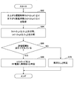
図5に示す第1実施形態に係る異常検知処理は、MC20により実行される。前提として、図6に示すように、時刻t0のSTART指令に従い、DOカウンタ40は、RF ON DO信号の回数Aをカウントし、DIカウンタ41は、RF ON DI信号の回数Bをカウントする。また、時刻t1のSTOP指令に従い、DOカウンタ40は、RF ON DO信号の回数Aのカウントを停止し、DIカウンタ41は、RF ON DI信号の回数Bのカウントを停止する。DOカウンタ40及びDIカウンタ41は、時刻trのRESET信号に従い初期化される。
図5に示す第1実施形態に係る異常検知処理は、MC20により実行される。前提として、図6に示すように、時刻t0のSTART指令に従い、DOカウンタ40は、RF ON DO信号の回数Aをカウントし、DIカウンタ41は、RF ON DI信号の回数Bをカウントする。また、時刻t1のSTOP指令に従い、DOカウンタ40は、RF ON DO信号の回数Aのカウントを停止し、DIカウンタ41は、RF ON DI信号の回数Bのカウントを停止する。DOカウンタ40及びDIカウンタ41は、時刻trのRESET信号に従い初期化される。
図5に示す異常検知処理が開始されると、制御部26は、RF電源18のオンを指令するDO信号の出力回数Xをカウントする(ステップS10)。通信部25は、I/Oボード30の通信部36からDOカウンタ40に格納されたカウント数A及びDIカウンタ41に格納されたカウント数Bを取得する(ステップS12)。
次に、異常判定部27は、出力回数Xがカウント数Aに等しいかを判定する(ステップS14)。異常判定部27は、出力回数Xがカウント数Aに等しくないと判定した場合、I/Oボード30に異常があると判定し(ステップS16)、本処理を終了する。他方、異常判定部27は、出力回数Xがカウント数Aに等しいと判定した場合、出力回数Xがカウント数Bに等しいかを判定する(ステップS18)。
異常判定部27は、出力回数Xがカウント数Bに等しいと判定した場合、異常なしと判定し(ステップS20)、本処理を終了する。他方、異常判定部27は、出力回数Xがカウント数Bに等しくないと判定した場合、I/Oボード30とRF電源18との間の配線又はRF電源18に異常があると判定し(ステップS22)、本処理を終了する。
以上、第1実施形態に係る異常検知システムによれば、基板処理装置10に設けられたRF電源18、I/Oボード30、及びRF電源18とI/Oボード30との間の配線の異常を検知することができる。
<第2実施形態>
次に、第2実施形態に係る状態信号検出回路及び第2実施形態に係る異常検知処理の一例について、図7~図10を参照しながら説明する。図7は、第2実施形態に係る状態信号検出回路の一例を示す。図8は、第1~第6実施形態に係る状態信号(DO,DI,AI信号)を説明するためのタイムチャートである。図9は、第2~第5実施形態に係る異常検知処理の一例を示すフローチャートである。図10は、第2実施形態に係る異常検知処理の一例を説明するためのタイムチャートである。
次に、第2実施形態に係る状態信号検出回路及び第2実施形態に係る異常検知処理の一例について、図7~図10を参照しながら説明する。図7は、第2実施形態に係る状態信号検出回路の一例を示す。図8は、第1~第6実施形態に係る状態信号(DO,DI,AI信号)を説明するためのタイムチャートである。図9は、第2~第5実施形態に係る異常検知処理の一例を示すフローチャートである。図10は、第2実施形態に係る異常検知処理の一例を説明するためのタイムチャートである。
(状態信号検出回路)
図7に示す第2実施形態に係る状態信号検出回路35は、FPGA回路34内にあり、AI回路51と最大値レジスタ42と最小値レジスタ43とを有する。AI回路51は、RF進行波の電力Pfのアナログ信号を12ビットのデータにディジタル化したPf AI信号を出力する。また、RF反射波の電力Prのアナログ信号を12ビットのデータにディジタル化したPr AI信号を出力する。
図7に示す第2実施形態に係る状態信号検出回路35は、FPGA回路34内にあり、AI回路51と最大値レジスタ42と最小値レジスタ43とを有する。AI回路51は、RF進行波の電力Pfのアナログ信号を12ビットのデータにディジタル化したPf AI信号を出力する。また、RF反射波の電力Prのアナログ信号を12ビットのデータにディジタル化したPr AI信号を出力する。
図10に示すように、時刻t3にSTART指令信号が出力され、時刻t4にSTOP指令信号が出力され、時刻trにRESET信号が出力される。時刻t3のSTART指令と時刻t4のSTOP指令の間に、例えば300μsのサンプリングクロックごとにデータがサンプリングされる。実際には、図8に示すように、START指令からSTOP指令の間は、一プロセスを示し、サンプリング時間は、一プロセス内の50ms~100msの範囲の所定時間である。図10に示すサンプリングクロックに応じて収集されるサンプリングデータのうち、Pf AI信号の最大値及びPr AI信号の最大値は、それぞれ最大値レジスタ42に格納される。また、Pf AI信号の最小値及びPr AI信号の最小値は、それぞれ最小値レジスタ43に格納される。
最大値レジスタ42及び最小値レジスタ43は、それぞれ12ビットとし、MC20のMCソフトウェアにより制御されるSTART指令により最大値及び最小値の検出を開始し、STOP指令によりその検出を停止する。また、最大値レジスタ42及び最小値レジスタ43は、RESET指令により初期化される。
なお、最大値レジスタ42及び最小値レジスタ43のレジスタ値の読み取りは、検出中でも可能である。また、検出可能なAI信号数はFPGA回路34の設計により増減可能である。
基板処理装置10がプラズマALD装置の場合、一プロセスは200ms~800msで行われる。よって、図8に示すように、Pf AI信号のSTART指令(t0,t3、・・・)及びSTOP指令(t2,t4、・・・)のそれぞれの間隔は、200ms~800msとなる。よって、200ms~800msの一プロセス毎に一回のサンプリングデータが収集される。
サンプリングデータは、50ms~100msの範囲の所定時間内において300μs~1msのサンプリング間隔で収集される。例えば、50msの所定時間内において300μs毎に複数個のPf AI信号及びPr AI信号のサンプリングデータが収集されることになる。収集されたPf AI信号及びPr AI信号のサンプリングデータは、I/Oボード30の記憶部37に記憶される。
このように、第1実施形態のSTART指令(t0)からSTOP指令(t1)までの時間は、300回程度のプロセスが包含されるため、第2実施形態のSTART指令(t0,t3、・・・)からSTOP指令(t2,t4、・・・)までの時間よりも長い。
MC20は、例えば100ms毎にポーリングを行う。MC20がAI信号のサンプリングデータを取得する周期は、例えばALD法による処理の一サイクル200~800msのうちの所定時間50ms~100msよりも長いか又は同じ時間である。よって、MC20の一回のポーリングによって、MC20が取得するAI信号のサンプリングデータは、一回分のAI信号のサンプリングデータであり、一回のポーリングにて複数回分のAI信号のサンプリングデータを取得することはない。
(異常検知処理)
図9に示す第2実施形態に係る異常検知処理は、MC20により実行される。本処理が開始されると、制御部26は、ポーリングのタイミングに同期して、通信部25を介して所定のサンプリング間隔(本実施形態では、300μs)で収集されたサンプリングデータのPf(RFの進行波電力)のAI信号の最大値と最小値、及びPr(RFの反射波電力)のAI信号の最大値と最小値をI/Oボード30から受信する(ステップS32)。
図9に示す第2実施形態に係る異常検知処理は、MC20により実行される。本処理が開始されると、制御部26は、ポーリングのタイミングに同期して、通信部25を介して所定のサンプリング間隔(本実施形態では、300μs)で収集されたサンプリングデータのPf(RFの進行波電力)のAI信号の最大値と最小値、及びPr(RFの反射波電力)のAI信号の最大値と最小値をI/Oボード30から受信する(ステップS32)。
次に、異常判定部27は、PfのAI信号の最大値が所定の閾値Aよりも大きいか否かを判定する(ステップS34)。異常判定部27は、PfのAI信号の最大値が所定の閾値Aよりも大きいと判定した場合、RF電源18に異常があると判定し(ステップS36)、本処理を終了する。他方、異常判定部27は、PfのAI信号の最大値が所定の閾値A以下であると判定した場合、PfのAI信号の最小値が所定の閾値Bよりも小さいか否かを判定する(ステップS38)。
異常判定部27は、PfのAI信号の最小値が所定の閾値Bよりも小さいと判定した場合、RF電源18に異常があると判定し(ステップS36)、本処理を終了する。他方、異常判定部27は、PfのAI信号の最小値が所定の閾値B以上であると判定した場合、PrのAI信号の最大値が所定の閾値Cよりも大きいか否かを判定する(ステップS40)。異常判定部27は、PrのAI信号の最大値が所定の閾値Cよりも大きいと判定した場合、RF電源18に異常があると判定し(ステップS36)、本処理を終了する。他方、異常判定部27は、PrのAI信号の最大値が所定の閾値C以下であると判定した場合、PrのAI信号の最小値が所定の閾値Dよりも小さいか否かを判定する(ステップS42)。
異常判定部27は、PrのAI信号の最小値が所定の閾値Dよりも小さいと判定した場合、RF電源18に異常があると判定し(ステップS36)、本処理を終了する。他方、異常判定部27は、PrのAI信号の最小値が所定の閾値D以上であると判定した場合、機器に異常はないと判定し(ステップS44)、本処理を終了する。
なお、所定の閾値A~Dの一例としては、正常なプロセスを実施した際のPfのAI信号の中心値の±5%の範囲の値の最大値と最小値を閾値Aと閾値Bにそれぞれ設定してもよい。同様に、正常なプロセスを実施した際のPrのAI信号の中心値の±5%の範囲の値の最大値と最小値の値を閾値Cと閾値Dにそれぞれ設定してもよい。ただし、各閾値A~Dの設定は、これに限らず、正常なプロセスから逸脱しない範囲を示す他の許容値を用いることができる。
以上、第2実施形態に係る異常検知システムによれば、I/Oボード30は、PfのAI信号及びPrのAI信号のサンプリングデータを、MC20のポーリング周期以下の時間である、例えば300μsのサンプリング間隔で収集し、記憶部37に記憶する。これにより、収集したサンプリングデータを一時的にI/Oボード30に蓄積しておく。MC20は、ポーリング周期で、サンプリングデータをI/Oボード30から取得することで、蓄積したサンプリングデータに基づきRF電源18の異常を精度良く検知することができる。
なお、第2実施形態では、MC20は、Pf AI信号の最大値及び最小値及びPr AI信号の最大値及び最小値に基づき、RF電源18等の機器の異常の有無を判定したが、これに限らない。MC20は、ポーリング毎にI/Oボード30から取得したサンプリングデータのピーク値、平均値、中央値等を算出し、算出結果に基づき、機器の異常の有無を判定してもよい。
<第3実施形態>
次に、第3実施形態に係る状態信号検出回路及び第3実施形態に係る異常検知処理の一例について、図11及び図12を参照しながら説明する。図11は、第3実施形態に係る状態信号検出回路の一例を示す。図12は、第3実施形態に係る異常検知処理における各信号のタイムチャートである。
次に、第3実施形態に係る状態信号検出回路及び第3実施形態に係る異常検知処理の一例について、図11及び図12を参照しながら説明する。図11は、第3実施形態に係る状態信号検出回路の一例を示す。図12は、第3実施形態に係る異常検知処理における各信号のタイムチャートである。
(状態信号検出回路)
図11に示す第3実施形態に係る状態信号検出回路35は、FPGA回路34内にあり、AI回路51と最大値レジスタ42と最小値レジスタ43とを有する。AI回路51は、RF進行波の電圧Vppのアナログ信号を12ビットのデータにディジタル化したVpp AI信号を出力する。
図11に示す第3実施形態に係る状態信号検出回路35は、FPGA回路34内にあり、AI回路51と最大値レジスタ42と最小値レジスタ43とを有する。AI回路51は、RF進行波の電圧Vppのアナログ信号を12ビットのデータにディジタル化したVpp AI信号を出力する。
最大値レジスタ42及び最小値レジスタ43は、それぞれ12ビットとし、MC20のMCソフトウェアにより制御されるSTART指令に従い、Vpp AI信号の最大値及び最小値の検出を開始し、STOP指令によりその検出を停止する。また、最大値レジスタ42及び最小値レジスタ43は、RESET指令により初期化される。最大値レジスタ42及び最小値レジスタ43のレジスタ値の読み取りは、検出中でも可能である。
図12に示すように、時刻t3にSTART指令信号が出力され、時刻t4にSTOP指令信号が出力され、時刻trにRESET信号が出力される。時刻t3のSTART指令と時刻t4のSTOP指令の間であって、例えば300μsのサンプリングクロックごとにデータがサンプリングされる。サンプリングデータのうち、Vpp AI信号の最大値が最大値レジスタ42に格納され、Vpp AI信号の最小値が最小値レジスタ43に格納される。
第2実施形態の場合と同様に、サンプリングデータは、200ms~800msの一プロセス毎に50ms~100msの範囲内の所定時間、300μsのサンプリング間隔で収集される。本実施形態では、50msの所定時間、300μs毎にVpp AI信号のデータが収集されることになる。収集されたVpp AI信号のサンプリングデータは、I/Oボード30の記憶部37に記憶される。
(異常検知処理)
第2実施形態と同様に、MC20は、ポーリング毎にI/Oボード30から取得したサンプリングデータの最大値及び最小値に基づき、RF電源18等の機器の異常の有無を判定する。具体的には、図9の異常検知処理で使用されたサンプリングデータが、Pf AI信号及びPr AI信号のサンプリングデータであったのに対して、本実施形態は、Vpp AI信号のサンプリングデータを使用して、図9の異常検知処理と同様な処理を行う。つまり、Vpp AI信号の最大値が所定の閾値Eより大きい場合、又は、Vpp AI信号の最小値が所定の閾値Fより小さい場合、RF電源に異常ありと判定し、それ以外の場合、異常なしと判定して、処理を終了する。
第2実施形態と同様に、MC20は、ポーリング毎にI/Oボード30から取得したサンプリングデータの最大値及び最小値に基づき、RF電源18等の機器の異常の有無を判定する。具体的には、図9の異常検知処理で使用されたサンプリングデータが、Pf AI信号及びPr AI信号のサンプリングデータであったのに対して、本実施形態は、Vpp AI信号のサンプリングデータを使用して、図9の異常検知処理と同様な処理を行う。つまり、Vpp AI信号の最大値が所定の閾値Eより大きい場合、又は、Vpp AI信号の最小値が所定の閾値Fより小さい場合、RF電源に異常ありと判定し、それ以外の場合、異常なしと判定して、処理を終了する。
これにより、RF電源18の異常の有無を判定できる。なお、MC20は、ポーリング毎にI/Oボード30から取得したサンプリングデータのピーク値、平均値、中央値等を算出し、算出結果に基づき、機器の異常の有無を判定してもよい。
以上、第3実施形態に係る異常検知システムによれば、I/Oボード30は、Vpp AI信号のサンプリングデータを、MC20のポーリング周期以下の時間である、例えば300μsのサンプリング間隔で収集し、記憶部37に記憶する。これにより、収集したサンプリングデータを一時的にI/Oボード30に蓄積しておく。MC20は、ポーリング周期で、サンプリングデータをI/Oボード30から取得することで、蓄積したサンプリングデータに基づき、RF電源18の異常の有無を判定できる。
<第4実施形態>
次に、第4実施形態に係る状態信号検出回路及び第4実施形態に係る異常検知処理の一例について、図13及び図14を参照しながら説明する。図13は、第4実施形態に係る状態信号検出回路の一例を示す。図14は、第4実施形態に係る異常検知処理における各信号のタイムチャートである。
次に、第4実施形態に係る状態信号検出回路及び第4実施形態に係る異常検知処理の一例について、図13及び図14を参照しながら説明する。図13は、第4実施形態に係る状態信号検出回路の一例を示す。図14は、第4実施形態に係る異常検知処理における各信号のタイムチャートである。
(状態信号検出回路)
図13に示す第4実施形態に係る状態信号検出回路35は、FPGA回路34内にあり、AI回路51と最大値レジスタ42と最小値レジスタ43とを有する。AI回路51は、整合器17の整合位置であるLoad PositionとTune Positionのアナログ信号を12ビットのデータにディジタル化したLoad AI信号とTune AI信号を出力する。
図13に示す第4実施形態に係る状態信号検出回路35は、FPGA回路34内にあり、AI回路51と最大値レジスタ42と最小値レジスタ43とを有する。AI回路51は、整合器17の整合位置であるLoad PositionとTune Positionのアナログ信号を12ビットのデータにディジタル化したLoad AI信号とTune AI信号を出力する。
最大値レジスタ42及び最小値レジスタ43は、それぞれ12ビットとし、MC20のMCソフトウェアにより制御されるSTART指令に従い、Load AI信号及びTune AI信号の最大値及び最小値の検出を開始し、STOP指令によりその検出を停止する。また、最大値レジスタ42及び最小値レジスタ43は、RESET指令により初期化される。なお、最大値レジスタ42及び最小値レジスタ43のレジスタ値の読み取りは、検出中でも可能である。
図14に示すように、時刻t3にSTART指令信号が出力され、時刻t4にSTOP指令信号が出力され、時刻trにRESET信号が出力される。時刻t3のSTART指令と時刻t4のSTOP指令の間であって、例えば300μsのサンプリングクロックごとにデータがサンプリングされる。サンプリングデータのうち、Load AI信号及びTune AI信号の最大値が最大値レジスタ42に格納され、Load AI信号及びTune AI信号の最小値が最小値レジスタ43に格納される。
第2実施形態の場合と同様に、サンプリングデータは、200ms~800msの一プロセス毎に50ms~100msの範囲内の所定時間、300μsのサンプリング間隔で収集される。本実施形態では、50msの所定時間、300μs毎にLoad AI信号及びTune AI信号のサンプリングデータが収集されることになる。収集されたLoad AI信号及びTune AI信号のサンプリングデータは、I/Oボード30の記憶部37に記憶される。
(異常検知処理)
第2実施形態と同様に、MC20は、ポーリング毎にI/Oボード30から取得したサンプリングデータの最大値及び最小値に基づき、整合器17の異常の有無を判定する。具体的には、図9の異常検知処理で使用されたサンプリングデータが、Pf AI信号及びPr AI信号のサンプリングデータであったのに対して、本実施形態は、整合器17のLoad AI信号及びTune AI信号のサンプリングデータを使用して、図9のPf AI信号及びPr AI信号をLoad AI信号及びTune AI信号に置き換えて、図9の異常検知処理と同一処理を行う。これにより、整合器17の異常の有無を判定できる。なお、MC20は、ポーリング毎にI/Oボード30から取得したサンプリングデータのピーク値、平均値、中央値等を算出し、算出結果に基づき、機器の異常の有無を判定してもよい。
第2実施形態と同様に、MC20は、ポーリング毎にI/Oボード30から取得したサンプリングデータの最大値及び最小値に基づき、整合器17の異常の有無を判定する。具体的には、図9の異常検知処理で使用されたサンプリングデータが、Pf AI信号及びPr AI信号のサンプリングデータであったのに対して、本実施形態は、整合器17のLoad AI信号及びTune AI信号のサンプリングデータを使用して、図9のPf AI信号及びPr AI信号をLoad AI信号及びTune AI信号に置き換えて、図9の異常検知処理と同一処理を行う。これにより、整合器17の異常の有無を判定できる。なお、MC20は、ポーリング毎にI/Oボード30から取得したサンプリングデータのピーク値、平均値、中央値等を算出し、算出結果に基づき、機器の異常の有無を判定してもよい。
以上、第4実施形態に係る異常検知システムによれば、I/Oボード30は、Load AI信号及びTune AI信号のサンプリングデータを、MC20のポーリング周期よりも短時間で収集する。これにより、収集したサンプリングデータを一時的にI/Oボード30に蓄積しておく。MC20は、ポーリング周期で、サンプリングデータをI/Oボード30から取得することで、蓄積したサンプリングデータに基づき、整合器17の異常の有無を判定できる。
<第5実施形態>
次に、第5実施形態に係る状態信号検出回路及び第5実施形態に係る異常検知処理の一例について、図15~図17を参照しながら説明する。図15は、第5実施形態に係る状態信号検出回路の一例を示す。図16は、第5実施形態に係る異常検知処理における各信号のタイムチャートである。図17は、第5実施形態に係る異常検知処理における積算方法を説明するための図である。
次に、第5実施形態に係る状態信号検出回路及び第5実施形態に係る異常検知処理の一例について、図15~図17を参照しながら説明する。図15は、第5実施形態に係る状態信号検出回路の一例を示す。図16は、第5実施形態に係る異常検知処理における各信号のタイムチャートである。図17は、第5実施形態に係る異常検知処理における積算方法を説明するための図である。
(状態信号検出回路)
図15に示す第5実施形態に係る状態信号検出回路35は、FPGA回路34内にあり、AI回路51と積算レジスタ44とを有する。AI回路51は、RF進行波の電力Pfのアナログ信号及びRF反射波の電力Prのアナログ信号を12ビットのデータにディジタル化したPf AI信号及びPr AI信号を出力する。
図15に示す第5実施形態に係る状態信号検出回路35は、FPGA回路34内にあり、AI回路51と積算レジスタ44とを有する。AI回路51は、RF進行波の電力Pfのアナログ信号及びRF反射波の電力Prのアナログ信号を12ビットのデータにディジタル化したPf AI信号及びPr AI信号を出力する。
積算レジスタ44は、32ビットとし、MCソフトウェアの制御によるSTART指令により、Pf AI信号及びPr AI信号の積算を開始し、STOP指令によりその積算を停止する。また、積算レジスタ44は、RESET指令により初期化される。
積算間隔は、AI回路51のサンプリング間隔である300μs~1msの範囲内の設定値と同一間隔である。本実施形態では、積算間隔は、300μsである。積算レジスタ44のレジスタ値の読み取りは積算中でも可能であるが、32ビットのデータは、16ビット×2回の読み取りサイクルになるため、この間に16ビット目から17ビット目への桁上がりが発生すると不正確な読み取り値となる。ただし、300μsの間隔で12ビットのデータを32ビットの積算レジスタ44に加算していくと、300μs×2(32-12)=5分までの積算が可能である。よって、積算レジスタ44は、ALD法による成膜の一サイクル毎にサンプリングするPf AI信号及びPr AI信号のサンプリングデータを積算するには十分であり、桁上がりが発生して積算値が不正確な値となることは生じない。
図16に示すように、積算クロックに応じたPf AI信号の値が、3,5,5,5,5,5,1・・・の場合、積算レジスタ44に格納される値は、3,8,13,18,23,28,29・・・となる。積算クロックに応じたPr AI信号の値が、3,0,0,0,0,0,0・・・の場合、積算レジスタ44に格納される値は、3,3,3,3,3,3,3・・・となる。積算クロックは、サンプリングクロックと同期しており、例えば300μsのサンプリングクロックごとにデータがサンプリングされる場合、300μsの積算クロックごとにサンプリングデータが積算される。CPU32は、下記の式(1)を使用して、Pf AI信号及びPr AI信号のサンプリングデータの積算値を算出し、積算レジスタ44に格納する。
(異常検知処理)
MC20は、ポーリング毎にI/Oボード30から取得した、Pf AI信号及びPr AI信号のサンプリングデータの積算値を取得する。MC20は、積算結果に基づき、ALDの1サイクルにおけるRF電源18の異常の有無を判定する。また、MC20は、ALDの1サイクルごとの積算値を合計することで、一プロセスにおけるRF電源18の異常の有無を判定する。なお、算出したALDの1サイクルの積算値は、積算レジスタ44に蓄積され、MC20が、積算レジスタ44に蓄積された積算値を収集して、1プロセスの積算値を算出する。
MC20は、ポーリング毎にI/Oボード30から取得した、Pf AI信号及びPr AI信号のサンプリングデータの積算値を取得する。MC20は、積算結果に基づき、ALDの1サイクルにおけるRF電源18の異常の有無を判定する。また、MC20は、ALDの1サイクルごとの積算値を合計することで、一プロセスにおけるRF電源18の異常の有無を判定する。なお、算出したALDの1サイクルの積算値は、積算レジスタ44に蓄積され、MC20が、積算レジスタ44に蓄積された積算値を収集して、1プロセスの積算値を算出する。

積算値は、RFの進行波の総電力及びRFの反射波の総電力を示す。よって、積算値が予め定められた所定の閾値の範囲から外れている場合、異常判定部27は、RF電源18が異常であると判定する。
以上、第5実施形態に係る異常検知システムによれば、収集したPf AI信号及びPr AI信号のサンプリングデータに基づく積算値を一時的にI/Oボード30に蓄積しておき、MC20は、ポーリングに応じて積算値をI/Oボード30から取得する。これにより、RF電源18の出力の積算値に基づきRF電源18の異常を精度良く検知することができる。
<第6実施形態>
次に、第6実施形態に係る状態信号検出回路及び第6実施形態に係る異常検知処理の一例について、図18~図20を参照しながら説明する。図18は、第6実施形態に係る状態信号検出回路の一例を示す。図19は、第6実施形態に係る異常検知処理の一例を示すフローチャートである。図20は、第6実施形態に係る異常検知処理における各信号のタイムチャートである。
次に、第6実施形態に係る状態信号検出回路及び第6実施形態に係る異常検知処理の一例について、図18~図20を参照しながら説明する。図18は、第6実施形態に係る状態信号検出回路の一例を示す。図19は、第6実施形態に係る異常検知処理の一例を示すフローチャートである。図20は、第6実施形態に係る異常検知処理における各信号のタイムチャートである。
(状態信号検出回路)
図18に示す第6実施形態に係る状態信号検出回路35は、FPGA回路34内にあり、フォトカプラ50と立上がり遅延時間カウンタ45と立下がり遅延時間カウンタ46とを有する。
図18に示す第6実施形態に係る状態信号検出回路35は、FPGA回路34内にあり、フォトカプラ50と立上がり遅延時間カウンタ45と立下がり遅延時間カウンタ46とを有する。
立上がり遅延時間カウンタ45及び立下がり遅延時間カウンタ46は、MC20からRF電源18のオンを指令するDO信号と、DO信号に対する確認信号であるDI信号との間の相対的な時間差を計測する。
立上がり遅延時間カウンタ45は、DO信号とDI信号との立上がりにおける時間差を計測する。立下がり遅延時間カウンタ46は、DO信号とDI信号との立下がりにおける時間差を計測する。
立上がり遅延時間カウンタ45及び立下がり遅延時間カウンタ46は、それぞれ16ビットとし、MC20のMCソフトウェアが制御するSTART指令によりカウントを開始し、STOP指令によりそのカウントを停止する。立上がり遅延時間カウンタ45及び立下がり遅延時間カウンタ46のカウンタ値の読み取りは、カウント中でも可能とする。
(異常検知処理)
図19に示す第6実施形態に係る異常検知処理は、MC20により実行される。前提として、制御部26は、予めRF電源18が正常に動作しているときのDO信号(RF ON DO)とDI信号(RF ON DI)との立上がりにおける基準遅延時間Δtaの値と、RF ON DO信号とRF ON DI信号との立下がりにおける基準遅延時間Δtbの値とを測定しておく。
図19に示す第6実施形態に係る異常検知処理は、MC20により実行される。前提として、制御部26は、予めRF電源18が正常に動作しているときのDO信号(RF ON DO)とDI信号(RF ON DI)との立上がりにおける基準遅延時間Δtaの値と、RF ON DO信号とRF ON DI信号との立下がりにおける基準遅延時間Δtbの値とを測定しておく。
本処理を行う前に、制御部26は、立上がりにおける基準遅延時間Δtaの値と、立下がりにおける基準遅延時間Δtbの値とを取得する。次に、本処理が開始されると、通信部25は、I/Oボード30の通信部36から、立上がり遅延時間カウンタ45に格納された立上がり遅延時間S(n)(=Δtan:1≦n)を取得する(ステップS62)。また、通信部25は、I/Oボード30の通信部36から、立下がり遅延時間カウンタ46に格納された立下がり遅延時間U(n)(Δtbn:1≦n)を取得する(ステップS62)。これにより、図20に示す立上がり遅延時間S(n)と、立下がり遅延時間U(n)とが取得される。
次に、異常判定部27は、立上がり遅延時間S(n)(=Δtan)と基準遅延時間Δtaの値とを比較し、また、立下がり遅延時間U(n)(=Δtbn)と基準遅延時間Δtbの値とを比較する(ステップS64)。立上がり遅延時間カウンタ45及び立下がり遅延時間カウンタ46は、それぞれ16ビットのカウンタであり、ΔtaとΔtbとは、0.1ms×216=6.5秒までのカウントが可能であり、十分なカウント時間が確保されている。
異常判定部27は、比較の結果、立上がり遅延時間S(n)のいずれか又は立下がり遅延時間U(n)のいずれかが許容範囲を超えてずれているかを判定する(ステップS66)。異常判定部27は、許容範囲を超えてずれていると判定した場合、I/Oボード30又はRF電源18に異常があると判定し(ステップS68)、本処理を終了する。他方、異常判定部27は、許容範囲を超えてずれていないと判定した場合、RF電源18に異常はないと判定し(ステップS70)、本処理を終了する。
以上、第6実施形態に係る異常検知システムによれば、RF ON DO信号とRF ON DI信号との立上がりの遅延時間又は立下がりの遅延時間に基づき、RF電源18又はI/Oボード30の異常を精度良く検知することができる。
以上、異常検知システム及び制御ボードを上記実施形態により説明したが、本発明にかかる異常検知システム及び制御ボードは上記実施形態に限定されるものではなく、本発明の範囲内で種々の変形及び改良が可能である。上記複数の実施形態に記載された事項は、矛盾しない範囲で組み合わせることができる。
例えば、RF電源18等の機器が異常であると判定された場合、MC20は、機器の状態情報をログ情報として記録することが好ましい。これにより、基板処理装置10にて実行されるプロセスを設計及び構築する場合、ログ情報を利用することでプロセスの不良を未然に防止することができる。
RF電源18の異常には、RF電源18の劣化及び破損が含まれる。また、I/Oボード30の異常には、I/Oボード30の不具合の可能性がある。よって、MC20は、異常と判定された機器毎に異なる対応をしてもよい。例えば、RF電源18が異常であると判定した場合、異常と判定された回数が例えば3回などの所定の回数以上になったら、プロセスを停止するようにしてもよい。I/Oボード30が異常であると判定した場合、異常と判定された回数によらず、直ちにI/Oボード30からの信号の入出力を停止してもよい。
また、本発明に係る基板処理装置は、容量結合型プラズマ(CCP:Capacitively Coupled Plasma)装置だけでなく、その他の基板処理装置に適用可能である。その他の基板処理装置としては、誘導結合型プラズマ(ICP:Inductively Coupled Plasma)、ラジアルラインスロットアンテナを用いたプラズマ処理装置、ヘリコン波励起型プラズマ(HWP:Helicon Wave Plasma)装置、電子サイクロトロン共鳴プラズマ(ECR:Electron Cyclotron Resonance Plasma)装置等であってもよい。
本明細書では、成膜対象の基板として半導体ウェハWについて説明したが、これに限らず、LCD(Liquid Crystal Display)、FPD(Flat Panel Display)等に用いられる各種基板や、フォトマスク、CD基板、プリント基板等であっても良い。
本国際出願は、2016年3月29日に出願された日本国特許出願2016-066052号に基づく優先権を主張するものであり、その全内容を本国際出願に援用する。
1:EC
2:ネットワーク
10:基板処理装置
11:処理容器
14:ガス供給源
16:排気装置
17:整合器
18:RF電源
19:ステージ
20:MC
21:I/O制御インターフェース
22:CPU
23:揮発性メモリ
24:不揮発性メモリ
25:通信部
26:制御部
27:異常判定部
28:ログ記憶部
30:I/Oボード
31:I/Oモジュール
32:CPU
33:RAM
34:FPGA
35:状態信号検出回路
36:通信部
37:記憶部
38:計時部
39:機器制御部
40:DOカウンタ
41:DIカウンタ
42:最大値レジスタ
43:最小値レジスタ
44:積算レジスタ
45:立上がり遅延時間カウンタ
46:立下がり遅延時間カウンタ
48:ネットワーク
50:フォトカプラ
51:AI回路
Claims (8)
- 基板処理装置を制御する第1のコントローラと、該第1のコントローラの指示に従い、前記基板処理装置に設けられた機器を制御する第2のコントローラとを有し、前記機器の異常を検知する異常検知システムであって、
前記第2のコントローラは、前記機器の状態信号を、所定の周期における所定時間、所定のサンプリング間隔で収集し、収集した該機器の状態信号を蓄積する記憶部を有し、
前記第1のコントローラは、蓄積した前記機器の状態信号を、前記所定時間以上の時間間隔で前記第2のコントローラから取得し、取得した前記機器の状態信号に基づき、前記機器の異常の有無を判定する異常判定部とを有する、
異常検知システム。 - 前記機器は、前記基板処理装置に設けられた高周波電源及び整合器の少なくともいずれかであり、
前記記憶部は、前記高周波電源への指令信号の数、該指令信号に対する確認信号の数、前記高周波電源が出力する高周波の進行波の電力の信号、前記高周波の反射波の電力の信号、前記高周波の進行波の電圧の信号、前記整合器の整合位置の信号、前記高周波の進行波の電力の積算値を示す信号、前記高周波電源への指令信号と該指令信号に対する確認信号の立上がりの遅延時間を示す信号、及び前記高周波電源への指令信号と該指令信号に対する確認信号の立下がりの遅延時間を示す信号の少なくとも一つの状態信号を蓄積する、
請求項1に記載の異常検知システム。 - 前記異常判定部は、前記高周波の進行波の電力の信号と、前記高周波の反射波の電力の信号と、前記高周波の進行波の電圧の信号と、前記整合器の整合位置の信号のそれぞれのピーク値、中央値及び平均値、及び前記高周波の進行波の電力の積算値の信号が示す電力積算値の少なくとも一つに基づき、前記高周波電源の異常の有無を判定する、
請求項2に記載の異常検知システム。 - 前記異常判定部は、前記高周波電源への指令信号の数及び該指令信号に対する確認信号の数の少なくともいずれかに基づき、前記高周波電源の異常、前記整合器の異常又は該高周波電源と該整合器との間の配線の異常の有無を判定する、
請求項2に記載の異常検知システム。 - 前記異常判定部は、前記高周波電源への指令信号と該指令信号に対する確認信号の立上がりの遅延時間の信号が示す遅延時間及び前記高周波電源への指令信号と該指令信号に対する確認信号の立下がり遅延時間の信号が示す遅延時間の少なくともいずれかに基づき、前記高周波電源の異常又は前記整合器の異常の有無を判定する、
請求項2に記載の異常検知システム。 - 前記異常判定部が前記機器に異常があると判定した場合、該機器の状態信号のログ情報を記憶するログ記憶部を有する、
請求項1に記載の異常検知システム。 - 前記基板処理装置は、ALD法により基板に成膜処理を行うALD装置である、
請求項1に記載の異常検知システム。 - 基板処理装置に設けられた機器の状態信号に基づき、前記機器の異常の有無を判定する第1のコントローラに接続され、前記機器を制御する制御ボードであって、
前記機器の状態信号を、所定の周期における所定時間、所定のサンプリング間隔で収集、収集した該機器の状態信号を蓄積する記憶部と、
前記第1のコントローラが前記所定時間以上の時間間隔で発信するポーリングに応じて、蓄積した前記機器の状態信号を送信する通信部とを有する、
制御ボード。
Priority Applications (3)
| Application Number | Priority Date | Filing Date | Title |
|---|---|---|---|
| US16/088,102 US11873560B2 (en) | 2016-03-29 | 2017-03-15 | Abnormality detection system and control board |
| CN201780021606.5A CN108884566B (zh) | 2016-03-29 | 2017-03-15 | 异常探测系统和控制板 |
| KR1020187028162A KR102220434B1 (ko) | 2016-03-29 | 2017-03-15 | 이상 검지 시스템 및 제어 보드 |
Applications Claiming Priority (2)
| Application Number | Priority Date | Filing Date | Title |
|---|---|---|---|
| JP2016066052A JP6695190B2 (ja) | 2016-03-29 | 2016-03-29 | 異常検知システム及び制御ボード |
| JP2016-066052 | 2016-03-29 |
Publications (1)
| Publication Number | Publication Date |
|---|---|
| WO2017169804A1 true WO2017169804A1 (ja) | 2017-10-05 |
Family
ID=59965331
Family Applications (1)
| Application Number | Title | Priority Date | Filing Date |
|---|---|---|---|
| PCT/JP2017/010496 WO2017169804A1 (ja) | 2016-03-29 | 2017-03-15 | 異常検知システム及び制御ボード |
Country Status (5)
| Country | Link |
|---|---|
| US (1) | US11873560B2 (ja) |
| JP (1) | JP6695190B2 (ja) |
| KR (1) | KR102220434B1 (ja) |
| CN (1) | CN108884566B (ja) |
| WO (1) | WO2017169804A1 (ja) |
Families Citing this family (3)
| Publication number | Priority date | Publication date | Assignee | Title |
|---|---|---|---|---|
| JP7454915B2 (ja) * | 2019-04-11 | 2024-03-25 | 東京エレクトロン株式会社 | 処理装置および処理方法 |
| JP2022120418A (ja) * | 2021-02-05 | 2022-08-18 | 東京エレクトロン株式会社 | 基板処理装置、基板処理システム及び異常検知方法 |
| JP2023180573A (ja) * | 2022-06-09 | 2023-12-21 | 東京エレクトロン株式会社 | 基板処理装置、制御システム、および制御方法 |
Citations (3)
| Publication number | Priority date | Publication date | Assignee | Title |
|---|---|---|---|---|
| WO2005057993A1 (ja) * | 2003-11-27 | 2005-06-23 | Daihen Corporation | 高周波電力供給システム |
| JP2013168131A (ja) * | 2012-01-16 | 2013-08-29 | Tokyo Electron Ltd | 処理装置及びバルブ動作確認方法 |
| JP2015015282A (ja) * | 2013-07-03 | 2015-01-22 | ルネサスエレクトロニクス株式会社 | 半導体装置の製造方法およびプラズマ処理装置 |
Family Cites Families (7)
| Publication number | Priority date | Publication date | Assignee | Title |
|---|---|---|---|---|
| JP3349455B2 (ja) * | 1998-09-30 | 2002-11-25 | 宮崎沖電気株式会社 | 半導体製造装置のための管理方法および管理システム |
| JP4754419B2 (ja) * | 2006-07-03 | 2011-08-24 | 学校法人立命館 | プラズマ異常放電診断方法、プラズマ異常放電診断システム及びコンピュータプログラム |
| JP5012701B2 (ja) * | 2008-07-02 | 2012-08-29 | パナソニック株式会社 | プラズマ処理装置およびプラズマ処理装置における放電状態監視方法 |
| CN101990707B (zh) * | 2008-09-30 | 2013-03-06 | 东京毅力科创株式会社 | 基板的异常载置状态的检测方法、基板处理方法、计算机可读取的存储介质以及基板处理装置 |
| US20130056154A1 (en) | 2011-06-27 | 2013-03-07 | Tokyo Electron Limited | Abnormality detecting unit and abnormality detecting method |
| JP5547763B2 (ja) * | 2012-03-16 | 2014-07-16 | 三井造船株式会社 | プラズマ生成方法、この方法を用いた薄膜形成方法及びプラズマ生成装置 |
| US8790743B1 (en) * | 2013-03-04 | 2014-07-29 | Asm Ip Holding B.V. | Method for controlling cyclic plasma-assisted process |
-
2016
- 2016-03-29 JP JP2016066052A patent/JP6695190B2/ja active Active
-
2017
- 2017-03-15 US US16/088,102 patent/US11873560B2/en active Active
- 2017-03-15 CN CN201780021606.5A patent/CN108884566B/zh active Active
- 2017-03-15 KR KR1020187028162A patent/KR102220434B1/ko active IP Right Grant
- 2017-03-15 WO PCT/JP2017/010496 patent/WO2017169804A1/ja active Application Filing
Patent Citations (3)
| Publication number | Priority date | Publication date | Assignee | Title |
|---|---|---|---|---|
| WO2005057993A1 (ja) * | 2003-11-27 | 2005-06-23 | Daihen Corporation | 高周波電力供給システム |
| JP2013168131A (ja) * | 2012-01-16 | 2013-08-29 | Tokyo Electron Ltd | 処理装置及びバルブ動作確認方法 |
| JP2015015282A (ja) * | 2013-07-03 | 2015-01-22 | ルネサスエレクトロニクス株式会社 | 半導体装置の製造方法およびプラズマ処理装置 |
Also Published As
| Publication number | Publication date |
|---|---|
| JP6695190B2 (ja) | 2020-05-20 |
| US11873560B2 (en) | 2024-01-16 |
| KR102220434B1 (ko) | 2021-02-24 |
| US20200299841A1 (en) | 2020-09-24 |
| CN108884566B (zh) | 2020-11-03 |
| KR20180118728A (ko) | 2018-10-31 |
| JP2017179425A (ja) | 2017-10-05 |
| CN108884566A (zh) | 2018-11-23 |
Similar Documents
| Publication | Publication Date | Title |
|---|---|---|
| WO2017169804A1 (ja) | 異常検知システム及び制御ボード | |
| TW201719749A (zh) | 半導體製造設備中的可消耗零件之耗損偵測 | |
| US11462444B2 (en) | Substrate container, controller, and abnormality detection method | |
| US20130183443A1 (en) | Processing apparatus and valve operation checking method | |
| US9708711B2 (en) | Processing apparatus and process status checking method | |
| KR20180027338A (ko) | 이상 검지 방법 및 반도체 제조 장치 | |
| TWI444835B (zh) | A master controller for correcting the sampling phase, a semiconductor device, and a method for correcting the same | |
| US20170004984A1 (en) | Substrate transfer apparatus and substrate transfer method | |
| US7212950B2 (en) | Methods and apparatus for equipment matching and characterization | |
| US8055368B2 (en) | Control device and control method of plasma processing system, and storage medium storing control program | |
| US10347464B2 (en) | Cycle-averaged frequency tuning for low power voltage mode operation | |
| CN208753281U (zh) | Foup装置 | |
| CN101206496A (zh) | 自动频率监视电路、电子装置、自动频率监视方法及程序 | |
| KR20060120438A (ko) | 플라즈마 공정의 비정상적 작동을 검출하는 방법 | |
| JP6842828B2 (ja) | 処理システム及び処理プログラム | |
| WO2020051001A1 (en) | Method and apparatus for measuring erosion and calibrating position for a moving process kit | |
| JP2007019431A (ja) | 基板処理監視装置、基板処理監視システム、基板処理監視プログラム及び記録媒体 | |
| JP6415971B2 (ja) | 基板処理装置、基板処理方法及び基板処理プログラムを記録した記録媒体 | |
| TWI525696B (zh) | 提供蝕刻腔室之製程指標的方法及形成半導體特徵部的方法 | |
| EP4312003A1 (en) | Capacitive sensor system for precursor level measurement and method therefor | |
| CN115812247A (zh) | 晶片状态检测 | |
| KR20230146449A (ko) | 처리 데이터의 해석 방법, 및 정보 처리 장치 | |
| TW202233025A (zh) | 電漿處理裝置之異常檢測方法及電漿處理裝置 | |
| JP2024514105A (ja) | プラズマシース特性を制御するためのシステムおよび方法 | |
| JPH0547619A (ja) | 半導体製造装置の稼働率計 |
Legal Events
| Date | Code | Title | Description |
|---|---|---|---|
| ENP | Entry into the national phase |
Ref document number: 20187028162 Country of ref document: KR Kind code of ref document: A |
|
| NENP | Non-entry into the national phase |
Ref country code: DE |
|
| 121 | Ep: the epo has been informed by wipo that ep was designated in this application |
Ref document number: 17774348 Country of ref document: EP Kind code of ref document: A1 |
|
| 122 | Ep: pct application non-entry in european phase |
Ref document number: 17774348 Country of ref document: EP Kind code of ref document: A1 |