WO2017169447A1 - 半導体装置及び半導体装置の製造方法 - Google Patents
半導体装置及び半導体装置の製造方法 Download PDFInfo
- Publication number
- WO2017169447A1 WO2017169447A1 PCT/JP2017/007575 JP2017007575W WO2017169447A1 WO 2017169447 A1 WO2017169447 A1 WO 2017169447A1 JP 2017007575 W JP2017007575 W JP 2017007575W WO 2017169447 A1 WO2017169447 A1 WO 2017169447A1
- Authority
- WO
- WIPO (PCT)
- Prior art keywords
- semiconductor layer
- electrode
- semiconductor
- semiconductor device
- conductivity type
- Prior art date
- Legal status (The legal status is an assumption and is not a legal conclusion. Google has not performed a legal analysis and makes no representation as to the accuracy of the status listed.)
- Ceased
Links
Images










Classifications
-
- H—ELECTRICITY
- H10—SEMICONDUCTOR DEVICES; ELECTRIC SOLID-STATE DEVICES NOT OTHERWISE PROVIDED FOR
- H10D—INORGANIC ELECTRIC SEMICONDUCTOR DEVICES
- H10D8/00—Diodes
- H10D8/50—PIN diodes
-
- H—ELECTRICITY
- H10—SEMICONDUCTOR DEVICES; ELECTRIC SOLID-STATE DEVICES NOT OTHERWISE PROVIDED FOR
- H10D—INORGANIC ELECTRIC SEMICONDUCTOR DEVICES
- H10D12/00—Bipolar devices controlled by the field effect, e.g. insulated-gate bipolar transistors [IGBT]
- H10D12/411—Insulated-gate bipolar transistors [IGBT]
- H10D12/441—Vertical IGBTs
-
- H—ELECTRICITY
- H10—SEMICONDUCTOR DEVICES; ELECTRIC SOLID-STATE DEVICES NOT OTHERWISE PROVIDED FOR
- H10D—INORGANIC ELECTRIC SEMICONDUCTOR DEVICES
- H10D12/00—Bipolar devices controlled by the field effect, e.g. insulated-gate bipolar transistors [IGBT]
- H10D12/411—Insulated-gate bipolar transistors [IGBT]
- H10D12/441—Vertical IGBTs
- H10D12/461—Vertical IGBTs having non-planar surfaces, e.g. having trenches, recesses or pillars in the surfaces of the emitter, base or collector regions
- H10D12/481—Vertical IGBTs having non-planar surfaces, e.g. having trenches, recesses or pillars in the surfaces of the emitter, base or collector regions having gate structures on slanted surfaces, on vertical surfaces, or in grooves, e.g. trench gate IGBTs
-
- H—ELECTRICITY
- H10—SEMICONDUCTOR DEVICES; ELECTRIC SOLID-STATE DEVICES NOT OTHERWISE PROVIDED FOR
- H10D—INORGANIC ELECTRIC SEMICONDUCTOR DEVICES
- H10D30/00—Field-effect transistors [FET]
- H10D30/01—Manufacture or treatment
- H10D30/021—Manufacture or treatment of FETs having insulated gates [IGFET]
- H10D30/028—Manufacture or treatment of FETs having insulated gates [IGFET] of double-diffused metal oxide semiconductor [DMOS] FETs
- H10D30/0291—Manufacture or treatment of FETs having insulated gates [IGFET] of double-diffused metal oxide semiconductor [DMOS] FETs of vertical DMOS [VDMOS] FETs
-
- H—ELECTRICITY
- H10—SEMICONDUCTOR DEVICES; ELECTRIC SOLID-STATE DEVICES NOT OTHERWISE PROVIDED FOR
- H10D—INORGANIC ELECTRIC SEMICONDUCTOR DEVICES
- H10D30/00—Field-effect transistors [FET]
- H10D30/01—Manufacture or treatment
- H10D30/021—Manufacture or treatment of FETs having insulated gates [IGFET]
- H10D30/028—Manufacture or treatment of FETs having insulated gates [IGFET] of double-diffused metal oxide semiconductor [DMOS] FETs
- H10D30/0291—Manufacture or treatment of FETs having insulated gates [IGFET] of double-diffused metal oxide semiconductor [DMOS] FETs of vertical DMOS [VDMOS] FETs
- H10D30/0297—Manufacture or treatment of FETs having insulated gates [IGFET] of double-diffused metal oxide semiconductor [DMOS] FETs of vertical DMOS [VDMOS] FETs using recessing of the gate electrodes, e.g. to form trench gate electrodes
-
- H—ELECTRICITY
- H10—SEMICONDUCTOR DEVICES; ELECTRIC SOLID-STATE DEVICES NOT OTHERWISE PROVIDED FOR
- H10D—INORGANIC ELECTRIC SEMICONDUCTOR DEVICES
- H10D30/00—Field-effect transistors [FET]
- H10D30/60—Insulated-gate field-effect transistors [IGFET]
-
- H—ELECTRICITY
- H10—SEMICONDUCTOR DEVICES; ELECTRIC SOLID-STATE DEVICES NOT OTHERWISE PROVIDED FOR
- H10D—INORGANIC ELECTRIC SEMICONDUCTOR DEVICES
- H10D30/00—Field-effect transistors [FET]
- H10D30/60—Insulated-gate field-effect transistors [IGFET]
- H10D30/64—Double-diffused metal-oxide semiconductor [DMOS] FETs
- H10D30/66—Vertical DMOS [VDMOS] FETs
-
- H—ELECTRICITY
- H10—SEMICONDUCTOR DEVICES; ELECTRIC SOLID-STATE DEVICES NOT OTHERWISE PROVIDED FOR
- H10D—INORGANIC ELECTRIC SEMICONDUCTOR DEVICES
- H10D30/00—Field-effect transistors [FET]
- H10D30/60—Insulated-gate field-effect transistors [IGFET]
- H10D30/64—Double-diffused metal-oxide semiconductor [DMOS] FETs
- H10D30/66—Vertical DMOS [VDMOS] FETs
- H10D30/668—Vertical DMOS [VDMOS] FETs having trench gate electrodes, e.g. UMOS transistors
-
- H—ELECTRICITY
- H10—SEMICONDUCTOR DEVICES; ELECTRIC SOLID-STATE DEVICES NOT OTHERWISE PROVIDED FOR
- H10D—INORGANIC ELECTRIC SEMICONDUCTOR DEVICES
- H10D62/00—Semiconductor bodies, or regions thereof, of devices having potential barriers
- H10D62/10—Shapes, relative sizes or dispositions of the regions of the semiconductor bodies; Shapes of the semiconductor bodies
- H10D62/102—Constructional design considerations for preventing surface leakage or controlling electric field concentration
- H10D62/103—Constructional design considerations for preventing surface leakage or controlling electric field concentration for increasing or controlling the breakdown voltage of reverse-biased devices
- H10D62/105—Constructional design considerations for preventing surface leakage or controlling electric field concentration for increasing or controlling the breakdown voltage of reverse-biased devices by having particular doping profiles, shapes or arrangements of PN junctions; by having supplementary regions, e.g. junction termination extension [JTE]
- H10D62/106—Constructional design considerations for preventing surface leakage or controlling electric field concentration for increasing or controlling the breakdown voltage of reverse-biased devices by having particular doping profiles, shapes or arrangements of PN junctions; by having supplementary regions, e.g. junction termination extension [JTE] having supplementary regions doped oppositely to or in rectifying contact with regions of the semiconductor bodies, e.g. guard rings with PN or Schottky junctions
-
- H—ELECTRICITY
- H10—SEMICONDUCTOR DEVICES; ELECTRIC SOLID-STATE DEVICES NOT OTHERWISE PROVIDED FOR
- H10D—INORGANIC ELECTRIC SEMICONDUCTOR DEVICES
- H10D62/00—Semiconductor bodies, or regions thereof, of devices having potential barriers
- H10D62/10—Shapes, relative sizes or dispositions of the regions of the semiconductor bodies; Shapes of the semiconductor bodies
- H10D62/102—Constructional design considerations for preventing surface leakage or controlling electric field concentration
- H10D62/103—Constructional design considerations for preventing surface leakage or controlling electric field concentration for increasing or controlling the breakdown voltage of reverse-biased devices
- H10D62/105—Constructional design considerations for preventing surface leakage or controlling electric field concentration for increasing or controlling the breakdown voltage of reverse-biased devices by having particular doping profiles, shapes or arrangements of PN junctions; by having supplementary regions, e.g. junction termination extension [JTE]
- H10D62/109—Reduced surface field [RESURF] PN junction structures
- H10D62/111—Multiple RESURF structures, e.g. double RESURF or 3D-RESURF structures
-
- H—ELECTRICITY
- H10—SEMICONDUCTOR DEVICES; ELECTRIC SOLID-STATE DEVICES NOT OTHERWISE PROVIDED FOR
- H10D—INORGANIC ELECTRIC SEMICONDUCTOR DEVICES
- H10D62/00—Semiconductor bodies, or regions thereof, of devices having potential barriers
- H10D62/10—Shapes, relative sizes or dispositions of the regions of the semiconductor bodies; Shapes of the semiconductor bodies
- H10D62/113—Isolations within a component, i.e. internal isolations
- H10D62/115—Dielectric isolations, e.g. air gaps
-
- H—ELECTRICITY
- H10—SEMICONDUCTOR DEVICES; ELECTRIC SOLID-STATE DEVICES NOT OTHERWISE PROVIDED FOR
- H10D—INORGANIC ELECTRIC SEMICONDUCTOR DEVICES
- H10D62/00—Semiconductor bodies, or regions thereof, of devices having potential barriers
- H10D62/10—Shapes, relative sizes or dispositions of the regions of the semiconductor bodies; Shapes of the semiconductor bodies
- H10D62/113—Isolations within a component, i.e. internal isolations
- H10D62/115—Dielectric isolations, e.g. air gaps
- H10D62/116—Dielectric isolations, e.g. air gaps adjoining the input or output regions of field-effect devices, e.g. adjoining source or drain regions
-
- H—ELECTRICITY
- H10—SEMICONDUCTOR DEVICES; ELECTRIC SOLID-STATE DEVICES NOT OTHERWISE PROVIDED FOR
- H10D—INORGANIC ELECTRIC SEMICONDUCTOR DEVICES
- H10D62/00—Semiconductor bodies, or regions thereof, of devices having potential barriers
- H10D62/10—Shapes, relative sizes or dispositions of the regions of the semiconductor bodies; Shapes of the semiconductor bodies
- H10D62/124—Shapes, relative sizes or dispositions of the regions of semiconductor bodies or of junctions between the regions
- H10D62/126—Top-view geometrical layouts of the regions or the junctions
- H10D62/127—Top-view geometrical layouts of the regions or the junctions of cellular field-effect devices, e.g. multicellular DMOS transistors or IGBTs
-
- H—ELECTRICITY
- H10—SEMICONDUCTOR DEVICES; ELECTRIC SOLID-STATE DEVICES NOT OTHERWISE PROVIDED FOR
- H10D—INORGANIC ELECTRIC SEMICONDUCTOR DEVICES
- H10D64/00—Electrodes of devices having potential barriers
- H10D64/20—Electrodes characterised by their shapes, relative sizes or dispositions
- H10D64/23—Electrodes carrying the current to be rectified, amplified, oscillated or switched, e.g. sources, drains, anodes or cathodes
-
- H—ELECTRICITY
- H10—SEMICONDUCTOR DEVICES; ELECTRIC SOLID-STATE DEVICES NOT OTHERWISE PROVIDED FOR
- H10D—INORGANIC ELECTRIC SEMICONDUCTOR DEVICES
- H10D8/00—Diodes
-
- H—ELECTRICITY
- H10—SEMICONDUCTOR DEVICES; ELECTRIC SOLID-STATE DEVICES NOT OTHERWISE PROVIDED FOR
- H10D—INORGANIC ELECTRIC SEMICONDUCTOR DEVICES
- H10D8/00—Diodes
- H10D8/01—Manufacture or treatment
- H10D8/045—Manufacture or treatment of PN junction diodes
-
- H—ELECTRICITY
- H10—SEMICONDUCTOR DEVICES; ELECTRIC SOLID-STATE DEVICES NOT OTHERWISE PROVIDED FOR
- H10D—INORGANIC ELECTRIC SEMICONDUCTOR DEVICES
- H10D8/00—Diodes
- H10D8/01—Manufacture or treatment
- H10D8/051—Manufacture or treatment of Schottky diodes
-
- H—ELECTRICITY
- H10—SEMICONDUCTOR DEVICES; ELECTRIC SOLID-STATE DEVICES NOT OTHERWISE PROVIDED FOR
- H10D—INORGANIC ELECTRIC SEMICONDUCTOR DEVICES
- H10D8/00—Diodes
- H10D8/60—Schottky-barrier diodes
-
- H—ELECTRICITY
- H10—SEMICONDUCTOR DEVICES; ELECTRIC SOLID-STATE DEVICES NOT OTHERWISE PROVIDED FOR
- H10D—INORGANIC ELECTRIC SEMICONDUCTOR DEVICES
- H10D62/00—Semiconductor bodies, or regions thereof, of devices having potential barriers
- H10D62/10—Shapes, relative sizes or dispositions of the regions of the semiconductor bodies; Shapes of the semiconductor bodies
- H10D62/124—Shapes, relative sizes or dispositions of the regions of semiconductor bodies or of junctions between the regions
- H10D62/126—Top-view geometrical layouts of the regions or the junctions
Definitions
- the present invention relates to a semiconductor device and a method for manufacturing the semiconductor device.
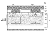
- a MOSFET that includes a semiconductor substrate in which a trench having a predetermined depth is formed on the surface of an n-type semiconductor layer and a p-type semiconductor layer made of an epitaxial layer is formed in the trench (for example, , See Patent Document 1).
- an n ⁇ -type second semiconductor layer 714 is stacked on an n + -type first semiconductor layer 712, and the surface of the second semiconductor layer 714 is formed in a predetermined direction.
- a plurality of trenches 718 arranged along a predetermined depth are formed, and a p ⁇ -type third semiconductor layer 716 made of an epitaxial layer is formed in the trench 718 (semiconductor substrate 710).
- a p-type base layer 720 is formed on a part of the surface of the second semiconductor layer 714 and the entire surface of the third semiconductor layer 716, and an n-type is formed on a part of the surface of the base layer 720.
- the first column 1C a portion of the second semiconductor layer 714 sandwiched between adjacent trenches 718 in a region deeper than the base layer 720 is the first column 1C, and the third semiconductor layer 716 is from the base layer 720.
- the deeper part is the second column 2C
- the first column 1C and the second column 2C form a super junction structure.
- the opening 728 is filled with the metal constituting the second electrode 724 as it is, and the second electrode 724 includes the third semiconductor layer 716 (specifically, the source region 740 and the base layer). 720).
- the third semiconductor layer 716 is formed by forming a trench 718 in the second semiconductor layer 714 and backfilling the trench 718 with a p-type epitaxial layer.
- the MOSFET 700 since the super-junction structure is configured by the first column 1C and the second column 2C in plan view, the MOSFET has characteristics of high breakdown voltage and low on-voltage.
- the trench 718 is formed in the n-type semiconductor layer (second semiconductor layer 714) and the trench 718 is backfilled with the p-type epitaxial layer, it is ideal that the entire inside of the trench 718 is completely backfilled.
- a cavity S (such as a slit-like cavity, a crevasse-like cavity, or a void-like cavity) may remain in the center of the third semiconductor layer 716 in plan view in the third semiconductor layer 716. Yes (see FIG. 21). Therefore, when making contact between the third semiconductor layer 716 and the second electrode 724, the metal of the second electrode 724 may enter the cavity S, and the metal inside the cavity S may become an electrode potential. .
- such a problem is not a problem that occurs only in the MOSFET but a problem that also occurs in the diode, IGBT, or the like.
- such a problem does not occur only when the trench of the n-type semiconductor layer is backfilled with the p-type epitaxial layer, but when the trench of the p-type semiconductor layer is backfilled with the n-type epitaxial layer. It is a problem that also occurs.
- such a problem is not only a problem that occurs only in a semiconductor device having a super junction structure, but also occurs in a semiconductor device that does not have a super junction structure.
- the present invention has been made to solve the above-described problems, and although it is a semiconductor device including a semiconductor substrate in which a third conductor layer made of an epitaxial layer is formed in a trench, a reach-through mode
- An object of the present invention is to provide a semiconductor device in which breakdown does not easily occur and breakdown voltage does not easily decrease. Moreover, it aims at providing the manufacturing method of the semiconductor device for manufacturing such a semiconductor device.
- a second semiconductor layer of the first conductivity type is stacked on the first semiconductor layer of the first conductivity type or the second conductivity type, and a predetermined surface is formed on the surface of the second semiconductor layer.
- a semiconductor device comprising an interlayer insulating film and a second electrode located on the interlayer insulating film, wherein the opening is filled with metal, wherein the opening is the third device when viewed in plan.
- the second electrode Located at a position avoiding the central portion of the semiconductor layer, the second electrode, It is connected to at least the third semiconductor layer through the metal filled in the mouth, and the surface of the central portion of the third semiconductor layer is covered with the interlayer insulating film.
- the first conductivity type impurity or the second conductivity type impurity is introduced into the surface of the second semiconductor layer or the third semiconductor layer to introduce another layer or another region (for example, the base layer or the first semiconductor layer). Even if a conductive type high concentration region or the like is formed, the other layer or the portion where the other region is formed is also the second semiconductor layer or the third semiconductor layer (see FIG. 22). However, a new trench is formed on the surface of the second semiconductor layer or the third semiconductor layer (different from the trench for forming the third semiconductor layer formed on the surface of the second semiconductor layer). In the case where a structure (for example, a trench gate structure or the like) different from the layer and the third semiconductor layer is formed, the structure is not the second semiconductor layer or the third semiconductor layer.
- a structure for example, a trench gate structure or the like
- the “predetermined depth” in “a plurality of trenches of a predetermined depth on the surface of the second semiconductor layer” is a depth reaching the boundary surface between the second semiconductor layer and the third semiconductor layer.
- the “interlayer insulating film” is formed between the electrode (second electrode) and the semiconductor substrate or between the electrode and another electrode (gate electrode), and between the electrode (second electrode) and the semiconductor substrate. Or a relatively thick insulating film that insulates between an electrode and another electrode (gate electrode).
- the “center portion of the third semiconductor layer in plan view” refers to a region near the midpoint of the sidewalls of the trenches facing each other in plan view, and “the third semiconductor layer in plan view”.
- the “center of” refers to the midpoint of the sidewalls of the trenches facing each other in plan view.
- the “opening” refers to a region where an interlayer insulating film is not formed, for example, a region where an interlayer insulating film is not formed even when the interlayer insulating film is formed in an island shape. Is called an opening.
- the length from the center of the third semiconductor layer to the side wall closest to the center of the third semiconductor layer among the side walls of the opening in a plan view is 0.1 ⁇ m or more. It is preferable that
- the semiconductor device of the present invention further includes a metal plug formed by filling the opening with a metal different from the metal constituting the second electrode, and the second electrode is interposed via the metal plug. It is preferable to be connected to at least the third semiconductor layer.
- the opening is filled with the metal constituting the second electrode as it is, and the second electrode is directly connected to at least the third semiconductor layer. Preferably it is.
- a fourth semiconductor layer of the second conductivity type is formed on at least a part of the surfaces of the second semiconductor layer and the third semiconductor layer in the semiconductor substrate, A portion deeper than the fourth semiconductor layer in the second semiconductor layer sandwiched between the adjacent trenches is defined as a first column, and a portion deeper than the fourth semiconductor layer in the third semiconductor layer is defined as a first column.
- a super junction structure is constituted by the first column and the second column.
- the fourth semiconductor layer is formed on the entire surface of the second semiconductor layer and the third semiconductor layer, and the second electrode is the fourth semiconductor.
- a PIN diode connected to the layer is preferred.
- the first semiconductor layer is a first conductivity type semiconductor layer
- the fourth semiconductor layer is the second semiconductor layer and the third semiconductor.
- a trench gate type MOSFET further comprising: a gate insulating film formed on an inner peripheral surface of the gate trench; and a gate electrode embedded in the gate trench through the gate insulating film, The electrode is preferably connected to the fourth semiconductor layer and the first conductivity type high concentration diffusion region.
- the first semiconductor layer is a first conductivity type semiconductor layer
- the fourth semiconductor layer is a part of the surface of the second semiconductor layer.
- a base layer formed on the entire surface of the third semiconductor layer a first conductivity type high concentration diffusion region is formed on a part of the surface of the fourth semiconductor layer
- the semiconductor device A planar gate type MOSFET further comprising a gate electrode formed through a gate insulating film so as to cover at least the fourth semiconductor layer sandwiched between the first conductivity type high concentration diffusion region and the second semiconductor layer
- the second electrode is preferably connected to the fourth semiconductor layer and the first conductivity type high concentration diffusion region.
- the first semiconductor layer is a semiconductor layer of a second conductivity type
- the fourth semiconductor layer is the second semiconductor layer and the third semiconductor.
- a trench gate type IGBT further comprising a gate trench formed, a gate insulating film formed on an inner peripheral surface of the gate trench, and a gate electrode embedded in the gate trench through the gate insulating film
- the second electrode is preferably connected to the fourth semiconductor layer and the first conductivity type high concentration diffusion region.
- the semiconductor device of the present invention in the semiconductor substrate, the first semiconductor layer is a second conductivity type semiconductor layer, and the fourth semiconductor layer is a part of the surface of the second semiconductor layer. And a base layer formed on the entire surface of the third semiconductor layer, a first conductivity type high concentration diffusion region is formed on a part of the surface of the fourth semiconductor layer, and the semiconductor device A planar gate type IGBT further comprising a gate electrode formed through a gate insulating film so as to cover at least the fourth semiconductor layer sandwiched between the first conductivity type high concentration diffusion region and the second semiconductor layer; The second electrode is preferably connected to the fourth semiconductor layer and the first conductivity type high concentration diffusion region.
- a second conductivity type high concentration diffusion region having an impurity concentration higher than that of the fourth semiconductor layer is formed immediately below the opening so as to be in contact with the bottom surface of the opening. It is preferable.
- the first column when the second semiconductor layer in the portion sandwiched between the adjacent trenches is the first column and the third semiconductor layer is the second column, the first column It is preferable that a super junction structure is constituted by the second column.
- the semiconductor device includes a Schottky barrier diode in which the metal is a barrier metal and the second electrode is connected to the second semiconductor layer in addition to the third semiconductor layer. It is preferable that
- the second semiconductor layer is preferably formed of a single crystal epitaxial layer.
- a first method for manufacturing a semiconductor device according to the present invention is a method for manufacturing a semiconductor device according to any one of [1] to [14], wherein the first conductivity type or A second semiconductor layer of the first conductivity type is stacked on the first semiconductor layer of the second conductivity type, and a trench having a predetermined depth is formed on the surface of the second semiconductor layer.
- a semiconductor substrate preparation step of preparing a semiconductor substrate on which a second conductive type third semiconductor layer made of a single crystal epitaxial layer is formed, and interlayer insulation on the surfaces of the second semiconductor layer and the third semiconductor layer An interlayer insulating film forming step of forming a film; an opening forming step of forming a predetermined opening in at least the region where the third semiconductor layer is formed in plan view in the interlayer insulating film; and an interior of the opening And the metal constituting the second electrode Forming a metal plug by filling the metal, forming a first electrode on the surface of the first semiconductor layer, and at least the first plug on the interlayer insulating film via the metal plug. An electrode forming step of forming a second electrode connected to the three semiconductor layers in this order.
- the opening is formed at a position avoiding the central portion of the third semiconductor layer in plan view.
- the opening forming step, the metal plug forming step, and the electrode forming step the surface of the central portion of the third semiconductor layer is covered with the interlayer insulating film.
- a second method for manufacturing a semiconductor device according to the present invention is a method for manufacturing a semiconductor device according to any one of [1] to [14], wherein the first conductivity type or A second semiconductor layer of the first conductivity type is stacked on the first semiconductor layer of the second conductivity type, and a trench having a predetermined depth is formed on the surface of the second semiconductor layer.
- a semiconductor substrate preparation step of preparing a semiconductor substrate on which a second conductive type third semiconductor layer made of a single crystal epitaxial layer is formed, and interlayer insulation on the surfaces of the second semiconductor layer and the third semiconductor layer An interlayer insulating film forming step of forming a film; an opening forming step of forming a predetermined opening at least in a region where the third semiconductor layer is formed in plan view in the interlayer insulating film; and the first semiconductor Process for forming the first electrode on the surface of the layer And an electrode forming process including a step of forming the second electrode on the interlayer insulating film filled with the metal constituting the second electrode as it is and directly connected to at least the third semiconductor layer.
- the opening is formed at a position avoiding the central portion of the third semiconductor layer in plan view, and in the opening forming step and the electrode forming step, The surface of the central part of the third semiconductor layer is covered with the interlayer insulating film.
- the opening is located at a position avoiding the central portion of the third semiconductor layer in plan view, and the surface of the central portion of the third semiconductor layer is covered with the interlayer insulating film. Therefore, when the third semiconductor layer is formed, a slit-like, crevasse-like, or void-like cavity remains in the center of the third semiconductor layer in plan view in the third semiconductor layer. However, when making contact between the third semiconductor layer and the second electrode, the metal of the second electrode does not enter the inside of the cavity, and the metal inside the cavity does not become the electrode potential.
- the depletion layer extending from the pn junction surface between the second semiconductor layer and the third semiconductor layer to the second electrode side only contacts the cavity.
- the semiconductor device is less likely to cause breakdown in reach-through mode and withstand voltage.
- the silicon surface inside the cavity is stabilized by oxidation in the oxidation process in the semiconductor pre-process, or dangling bonds are terminated by hydrogen in the annealing process, so that the depletion layer reaches the cavity. Even so, the depletion layer is merely in contact with the cavity, and this does not cause a sudden increase in leakage current or breakdown.
- the semiconductor device includes the interlayer insulating film having a predetermined opening formed at least in the region where the third semiconductor layer is formed in plan view. At the time of reverse recovery, holes generated in the third semiconductor layer can be easily extracted, and as a result, the L load avalanche breakdown resistance can be increased.
- the predetermined opening is formed in the interlayer insulating film at a position avoiding the central portion of the third semiconductor layer in plan view.
- the center surface of the third semiconductor layer is covered with an interlayer insulating film in the electrode forming step. Therefore, when the third semiconductor layer is formed, the inside of the third semiconductor layer is formed. Even when a slit-like, crevasse-like, or void-like cavity remains in the center of the third semiconductor layer in plan view, contact is made between the third semiconductor layer and the second electrode in the electrode forming step. At this time, the metal of the second electrode does not enter the inside of the cavity, and the metal inside the cavity does not become the electrode potential.
- the depletion layer extends from the pn junction surface between the second semiconductor layer and the third semiconductor layer to the second electrode side. Therefore, it is possible to manufacture a semiconductor device in which breakdown in the reach-through mode is unlikely to occur and the breakdown voltage is unlikely to decrease.
- the manufacturing method includes an opening forming step of forming a predetermined opening in at least the region where the third semiconductor layer is formed in plan view in the interlayer insulating film.
- the semiconductor device thus made can easily extract holes generated in the third semiconductor layer at the time of avalanche breakdown or reverse recovery of the body diode. As a result, a semiconductor device having a large L load avalanche breakdown resistance can be manufactured.
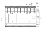
- FIG. 1 is a diagram illustrating a semiconductor device 100 according to a first embodiment.
- FIG. 1A is an enlarged cross-sectional view of a main part of the semiconductor device 100
- FIG. 1B is an enlarged plan view of the main part of the semiconductor device 100.
- FIG. 6 is an enlarged cross-sectional view of a main part for explaining the method for manufacturing the semiconductor device according to the first embodiment.
- 2A to 2D are process diagrams.
- FIG. 6 is an enlarged cross-sectional view of a main part for explaining the method for manufacturing the semiconductor device according to the first embodiment.
- 3A to 3D are process diagrams.
- FIG. 6 is an enlarged cross-sectional view of a main part for explaining the method for manufacturing the semiconductor device according to the first embodiment.
- 4A to 4C are process diagrams.
- FIG. 1A is an enlarged cross-sectional view of a main part of the semiconductor device 100
- FIG. 1B is an enlarged plan view of the main part of the semiconductor device 100.
- FIG. 6 is an enlarged cross-sectional view of a main part for explaining the method for manufacturing the semiconductor device according to the first embodiment.
- FIGS. 5A to 5C are process diagrams.
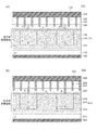
- FIG. 6 is a diagram for explaining the effect of the semiconductor device 100 according to the first embodiment.
- 6A is an enlarged cross-sectional view of the main part showing the state of the semiconductor device 100 at the time of reverse bias
- FIG. 6B is an enlarged cross-sectional view of the main part showing the state of the semiconductor device 900 according to the comparative example at the time of reverse bias.
- the semiconductor device 900 according to the comparative example basically has the same configuration as that of the semiconductor device 100 according to the first embodiment, but the opening 928 (and the metal plug 930) of the third semiconductor layer 916 is viewed in plan view. It is a semiconductor device formed in the central part.
- illustration of the p-type high concentration diffusion regions 132 and 932 is omitted for the sake of simplicity.
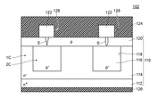
- FIG. 6 is an enlarged cross-sectional view showing a main part of a semiconductor device 102 according to a second embodiment.
- FIG. 6 is an enlarged cross-sectional view showing a main part of a semiconductor device 104 according to a third embodiment.
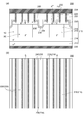
- FIG. 6 is a diagram illustrating a semiconductor device 200 according to a fourth embodiment.
- FIG. 9A is an enlarged cross-sectional view of the main part of the semiconductor device 200
- FIG. 9B is an enlarged plan view of the main part of the semiconductor device 200
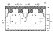
- FIG. 10 is an enlarged cross-sectional view showing a main part of a semiconductor device 202 according to a fifth embodiment.
- FIG. 10 is an enlarged cross-sectional view showing a main part of a semiconductor device 204 according to a sixth embodiment.
- FIG. 10 is an enlarged cross-sectional view showing a main part of a semiconductor device 300 according to a seventh embodiment.
- 10 is an enlarged cross-sectional view of a main part showing a semiconductor device 106 according to Modification 1.
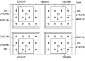
- FIG. 10 is an enlarged plan view of a main part showing a semiconductor device 200A according to Modification 2.
- FIG. 10 is an enlarged plan view of a main part showing a semiconductor device 200A according to Modification 2.
- FIG. 10 is an enlarged plan view of a main part showing a semiconductor device 200A according to Modification 2.
- the third semiconductor layer 216 has a quadrangular shape (columnar shape when viewed three-dimensionally) in plan view, and the gate electrode 238 (gate trench 234). Is a lattice shape when viewed in a plane, and the metal plug 230 (opening 228) is circular when viewed in a plane (a columnar shape when viewed in three dimensions).
- 10 is an enlarged plan view of a main part showing a semiconductor device 200B according to Modification 3.
- the third semiconductor layer 216 has a quadrangular shape (columnar shape when viewed three-dimensionally) when viewed in plan, and the gate electrode 238 (gate trench 234). Is a lattice shape when seen in a plan view, and the metal plug 230 (opening 228) is a frame shape when seen in a plan view.
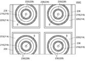
- FIG. 10 is an enlarged plan view of a main part showing a semiconductor device 200C according to Modification 4.
- the third semiconductor layer 216 has a circular shape (columnar shape when viewed three-dimensionally) when viewed in plan, and the metal plug 230 (opening 228) is formed.
- the gate electrode 238 has a lattice shape when viewed in a plan view.
- FIG. 10 is an enlarged plan view of a main part showing a semiconductor device 200D according to Modification 5.
- the third semiconductor layer 216 (trench 218) has a lattice shape when viewed in plan
- the gate electrode 238 (gate trench 234) has a quadrangular shape when viewed in plan.
- the metal plug 230 (opening 228) has a circular shape in a plan view (columnar shape in a three-dimensional view).
- FIG. 16 is an enlarged plan view of a main part showing a semiconductor device 200E according to Modification 6.
- the third semiconductor layer 216 (trench 218) has a quadrangular shape (columnar shape when viewed three-dimensionally) in plan view, and the gate electrode 238 (gate trench 234). Is a lattice shape when seen in a plan view, and the metal plug 230 (opening 228) is a lattice shape when seen in a plan view.
- 10 is an enlarged plan view of a main part showing a semiconductor device 200F according to Modification 7.
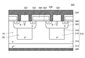
- FIG. 10 is an enlarged cross-sectional view of a main part showing a semiconductor device 302 according to Modification 8.
- FIG. It is a principal part expanded sectional view which shows the conventional MOSFET700. It is a figure which shows the semiconductor substrate in this specification. It is a principal part expanded sectional view shown in order to demonstrate the problem of the conventional MOSFET700.
- each drawing is a schematic diagram and does not necessarily reflect an actual dimension exactly.
- n ⁇ -type second semiconductor layer 114 is stacked on an n + -type first semiconductor layer 112 as shown in FIG.
- a plurality of trenches 118 having a predetermined depth arranged along a predetermined direction are formed on the surface of the second semiconductor layer 114, and a single crystal epitaxial layer is formed in the trench 118 (entirely in the trench 118).
- a semiconductor substrate on which a p ⁇ -type third semiconductor layer 116 made of the same is formed (refer to FIG. 22), and a first electrode 126 located on the surface of the first semiconductor layer 112.
- an interlayer insulation having a predetermined opening 128 formed on the surface of the second semiconductor layer 114 and the third semiconductor layer 116 and formed at least in a region where the third semiconductor layer 116 is formed in plan view.
- the second semiconductor layer 114 is formed of a single crystal epitaxial layer.
- a p-type fourth semiconductor layer 120 is formed on the entire surface of the second semiconductor layer 114 and the third semiconductor layer 116 in the semiconductor substrate 110.
- the impurity concentration p higher than that of the fourth semiconductor layer 120 is just below the opening 128.
- a + type high concentration diffusion region (second conductivity type high concentration diffusion region) 132 is formed in contact with the bottom surface of the opening 128.
- a portion deeper than the fourth semiconductor layer 120 in the second semiconductor layer 114 between the adjacent trenches 118 is defined as the first column 1C, and the third semiconductor layer 116 Of these, when the portion deeper than the fourth semiconductor layer 120 is the second column 2C, the first column 1C and the second column 2C form a super junction structure.
- the first column 1C and the second column 2C are in a charge balanced state.
- the thickness of the first semiconductor layer 112 is, for example, in the range of 100 ⁇ m to 400 ⁇ m, and the impurity concentration of the first semiconductor layer 112 is, for example, in the range of 1 ⁇ 10 19 cm ⁇ 3 to 1 ⁇ 10 20 cm ⁇ 3. is there.
- the thickness of the second semiconductor layer 114 (the thickness of the region where no trench is formed) is in the range of 5 ⁇ m to 120 ⁇ m, for example.
- the depth position of the deepest portion of the fourth semiconductor layer 120 is in the range of 0.5 ⁇ m to 2.0 ⁇ m, for example, and the impurity concentration of the fourth semiconductor layer 120 is, for example, 5 ⁇ 10 16 cm ⁇ 3 to 1 ⁇ 10. Within the range of 18 cm ⁇ 3 .
- the p + type high-concentration diffusion region 132 is in the range of 5 ⁇ 10 18 cm ⁇ 3 to 1 ⁇ 10 20 cm ⁇ 3 , for example.
- the trench 118 (third semiconductor layer 116), the opening 128, and the metal plug 130 are all formed in a stripe shape when seen in a plan view.
- the depth position of the bottom of the trench 118 is shallower than the depth position of the boundary surface between the first semiconductor layer 112 and the second semiconductor layer 114.
- the depth of the trench 118 is, for example, in the range of 3 ⁇ m to 115 ⁇ m.
- the width of the trench 118 is, for example, in the range of 3 ⁇ m to 10 ⁇ m.
- the spacing between adjacent trenches 118 is approximately the same as or preferably the same as the width of the trenches 118.
- the impurity concentrations of the second semiconductor layer 114 and the third semiconductor layer 116 are in the range of 5 ⁇ 10 14 cm ⁇ 3 to 5 ⁇ 10 16 cm ⁇ 3 , for example.
- the interlayer insulating film 122 is composed of a thermal oxide film 121 and a BPSG film.
- the thickness of the interlayer insulating film 122 is, for example, 1000 nm.
- the opening 128 is located at a position avoiding the central portion of the third semiconductor layer 116 in plan view, that is, at a position separated from the center of the third semiconductor layer 116 by a predetermined distance.
- the length from the center of the third semiconductor layer 116 to the side wall of the opening 128 closest to the center of the third semiconductor layer 116 is 0.1 ⁇ m or more, for example, 0.3 ⁇ m.
- the openings 128 are formed at equal intervals with a predetermined pitch, and the interval between the adjacent openings 128 is, for example, 0.7 ⁇ m.
- the opening width of the opening 128 is, for example, 0.5 ⁇ m.
- the opening 128 is formed to a depth position shallower than the depth position of the deepest portion of the fourth semiconductor layer 120.
- the center surface of the third semiconductor layer 116 is covered with an interlayer insulating film 122. Accordingly, no contact is made with the second electrode 124 at the center of the third semiconductor layer 116, and no trench is formed at the center of the third semiconductor layer 116.
- a barrier metal (not shown) is formed on the inner surface of the opening 128.
- the metal plug 130 is filled with metal inside the opening 128 through the barrier metal.
- the metal filling the opening 128 is, for example, tungsten.
- the first electrode (cathode electrode) 126 is formed of a multilayer metal film such as Ti—Ni—Au, and has a thickness of, for example, 0.5 ⁇ m over the entire multilayer metal film.
- the second electrode 124 is connected to the fourth semiconductor layer 120 formed on the third semiconductor layer 116 via the metal plug 130.
- the second electrode (anode electrode) 124 is made of an aluminum-based metal (for example, an Al—Cu alloy) having a thickness of, for example, 4 ⁇ m formed by sputtering.
- the second electrode 124 is also connected to the fourth semiconductor layer 120 formed on the second semiconductor layer 114 through the metal plug 130.
- the semiconductor device 100 according to the first embodiment can be manufactured by a manufacturing method (a manufacturing method of a semiconductor device according to the first embodiment) having the following manufacturing process.
- an n ⁇ -type second semiconductor layer 114 made of a single crystal epitaxial layer is stacked on an n + -type first semiconductor layer 112, and the surface of the second semiconductor layer 114 is A plurality of trenches 118 having a predetermined depth arranged along a predetermined direction are formed, and a p ⁇ -type third semiconductor layer 116 made of a single crystal epitaxial layer is formed in the trench 118.
- a semiconductor substrate 110 is prepared.
- a semiconductor substrate 110 ′ in which an n ⁇ -type second semiconductor layer 114 is stacked on an n + -type first semiconductor layer 112 is prepared (see FIG. 2A).
- the semiconductor substrate 110 ′ an appropriate semiconductor substrate can be used.
- a single crystal n ⁇ -type second semiconductor layer 114 is formed on the n + -type first semiconductor layer 112 by an epitaxial growth method.
- a semiconductor substrate can be used.
- a mask (not shown) having an opening corresponding to the third semiconductor layer 116 is formed on the surface of the second semiconductor layer 114, and etching is performed using the mask, whereby the second semiconductor layer 114 is formed.
- a plurality of trenches 118 having a predetermined depth arranged in a predetermined direction are formed (see FIG. 2B).
- a single crystal p ⁇ -type semiconductor layer 116 ′ is formed in the trench 118 by an epitaxial growth method (see FIGS. 2C, 2D, and 3A).
- a cavity S (a slit-like cavity, a crevice-like cavity, a void-like cavity, or the like) may remain in the center of the semiconductor layer 116 ′ in plan view in the center of the semiconductor layer 116 ′. Yes (see symbol S in FIG. 3A).
- the shape of the cavity is not only continuously connected (see FIG. 1B), but may be discontinuously connected or may be formed at only one place in an independent state. .
- the depth of the cavity S is shallower than the depth of the fourth semiconductor layer 120, but the present invention can be applied even when it is deeper than the depth of the fourth semiconductor layer 120.
- the p ⁇ -type third semiconductor layer 116 is formed by removing the semiconductor layer 116 ′ except for the inside of the trench 118 by CMP (see FIG. 3B). At this time, the cavity S may remain in the central portion of the third semiconductor layer 116 in plan view.
- a thermal oxide film (not shown) is formed on the entire surface of the second semiconductor layer 114 and the third semiconductor layer 116.
- p-type impurities for example, boron
- the fourth semiconductor layer 120 is formed on the entire surface of the second semiconductor layer 114 and the third semiconductor layer 116 by thermally diffusing the p-type impurity.
- a BPSG film is formed on the thermal oxide film by the CVD method, thereby forming the second semiconductor layer 114 and the third semiconductor layer 116 on the surface (the second semiconductor layer 114 and An interlayer insulating film 122 composed of a thermal oxide film (not shown) and a BPSG film is formed on the entire surface of the third semiconductor layer 116 (see FIG. 3D).
- a mask (not shown) having an opening in a region where the second semiconductor layer 114 and the third semiconductor layer 116 are formed on the interlayer insulating film 122 as viewed in a plan view. Form. At this time, in the mask, in the region where the third semiconductor layer 116 is formed in a plan view, an opening is provided at a position avoiding the central portion of the third semiconductor layer 116 in a plan view. ing. Next, by performing etching using the mask, a predetermined opening is formed in a region where the second semiconductor layer 114 and the third semiconductor layer 116 are formed in the interlayer insulating film as viewed in plan ( (See FIG. 4 (a)).
- a predetermined opening is formed at a position avoiding the central portion of the third semiconductor layer 116 in a plan view. Therefore, the central surface of the third semiconductor layer 116 is covered with the interlayer insulating film 122.
- Step of forming p-type high concentration diffusion region Next, p-type impurities (for example, boron) are ion-implanted into the bottom surface of the opening 128 at a higher impurity concentration than the fourth semiconductor layer 120 (see FIG. 4B). ). Next, by thermally diffusing the p-type impurity, a p-type high concentration diffusion region having an impurity concentration higher than that of the fourth semiconductor layer 120 is formed immediately below the opening so as to be in contact with the bottom surface of the opening 128 (FIG. 4). (See (c).)
- p-type impurities for example, boron
- the metal plug 130 is formed by filling the opening 128 with a metal different from the metal constituting the second electrode 124. Specifically, first, a barrier metal (not shown) is formed on the inner peripheral surface of the opening 128 by sputtering, and the barrier metal is annealed. Next, a tungsten film is formed on the barrier metal by a CVD method (see FIG. 5A). Next, the tungsten on the interlayer insulating film 122 is removed by CMP to leave the tungsten only in the opening 128 to form the metal plug 130 (see FIG. 5B).
- a barrier metal (not shown) is formed on the inner peripheral surface of the opening 128 by sputtering, and the barrier metal is annealed.
- a tungsten film is formed on the barrier metal by a CVD method (see FIG. 5A).
- the tungsten on the interlayer insulating film 122 is removed by CMP to leave the tungsten only in the opening 128 to form the metal plug 130 (see FIG. 5
- titanium nitride (TiN), titanium tungsten (TiW), molybdenum silicon (MoSi), or the like can be used. Even in the step of forming the metal plug 130, the surface of the central portion of the third semiconductor layer 116 is covered with the interlayer insulating film 122.
- Electrode Formation Step Next, a multilayer metal film such as Ti—Ni—Au is formed on the surface of the first semiconductor layer 112 to form the first electrode (cathode electrode) 126 and the third semiconductor layer.
- the surface of the central portion of the third semiconductor layer 116 is still covered with the interlayer insulating film 122, so that the metal of the second electrode 124 does not enter the cavity S.
- the semiconductor device 100 according to the first embodiment can be manufactured.
- the opening 128 is located at a position avoiding the central portion of the third semiconductor layer 116 in plan view, and Since the surface of the central portion is covered with the interlayer insulating film 122, when the third semiconductor layer 116 is formed, the cavity S in the third semiconductor layer 116 is seen in plan view in the center of the third semiconductor layer 116. Even when the second electrode 124 remains, the metal of the second electrode 124 does not enter the cavity S when making contact between the third semiconductor layer 116 and the second electrode 124. The metal is no longer at the electrode potential.
- the depletion layer extending from the pn junction surface between the second semiconductor layer 114 and the third semiconductor layer 116 to the second electrode 124 side is the cavity. Since it is only in contact with S, the breakdown of the reach-through mode is unlikely to occur and the breakdown voltage is unlikely to be reduced (see FIG. 6A).
- the silicon surface inside the cavity is oxidized in an oxidation process (for example, a process for forming a thermal oxide film in a fourth semiconductor layer formation process) in a semiconductor pre-process or an annealing process (for example, a fourth semiconductor layer formation process).
- an oxidation process for example, a process for forming a thermal oxide film in a fourth semiconductor layer formation process
- an annealing process for example, a fourth semiconductor layer formation process
- the interlayer insulating film 122 having a predetermined opening formed in the region where the third semiconductor layer 116 is formed in plan view since the interlayer insulating film 122 having a predetermined opening formed in the region where the third semiconductor layer 116 is formed in plan view, the avalanche breakdown is provided. At this time or during reverse recovery of the body diode, holes generated in the third semiconductor layer 116 can be easily extracted, and as a result, the L load avalanche breakdown resistance can be increased.
- the length from the center of the third semiconductor layer 116 to the side wall closest to the center of the third semiconductor layer 116 among the side walls of the opening 128 is 0 in plan view. Since it is 1 ⁇ m or more, the opening 128 (and the metal plug 130) can be prevented from communicating with the cavity S, and the metal constituting the metal plug 130 can be reliably prevented from entering the cavity S. . As a result, the breakdown of the reach-through mode is less likely to occur, and the semiconductor device is more unlikely to have a lower breakdown voltage. From this point of view, the length from the center of the third semiconductor layer 116 to the side wall closest to the center of the third semiconductor layer 116 among the side walls of the opening 128 when viewed in plan is 0.2 ⁇ m or more. preferable.
- the opening 128 includes the metal plug 130 in which a metal different from the metal constituting the second electrode 124 is filled, and the second electrode 124 has the metal plug 130. Therefore, the opening width of the opening 128 can be relatively small, and a miniaturized semiconductor device can be obtained. As a result, the semiconductor device meets the demand for cost reduction and downsizing of electronic devices.
- a portion deeper than the fourth semiconductor layer 120 in the second semiconductor layer 114 between the adjacent trenches 118 is defined as the first column 1C, and the third semiconductor.
- the first column 1C and the second column 2C form a super junction structure.
- the p-type high concentration diffusion region 132 having an impurity concentration higher than that of the fourth semiconductor layer 120 is formed immediately below the opening 128 so as to be in contact with the bottom surface of the opening 128. Therefore, holes can be easily extracted at the time of avalanche breakdown and reverse recovery of the diode.
- the semiconductor device 100 since the second semiconductor layer 114 is formed of a single crystal epitaxial layer, the conductivity of the second semiconductor layer 114 can be controlled with high accuracy, and Oxygen is less likely to be taken into the semiconductor substrate during the manufacturing process, so that crystal defects are less likely to occur and electrical defects are less likely to occur in the semiconductor device.
- the semiconductor device manufacturing method includes the opening forming step of forming the predetermined opening 128 in the interlayer insulating film 122 at a position avoiding the central portion of the third semiconductor layer 116 in plan view.
- the opening forming step of forming the predetermined opening 128 in the interlayer insulating film 122 at a position avoiding the central portion of the third semiconductor layer 116 in plan view.
- a slit shape is formed in the third semiconductor layer 116 when the third semiconductor layer 116 is formed. Even when the crevasse-like or void-like cavity S remains in the center of the third semiconductor layer 116 in plan view, the contact between the third semiconductor layer 116 and the second electrode 124 is made in the electrode forming step.
- the metal of the second electrode 124 does not enter the cavity S, and the metal inside the cavity S does not become the electrode potential. Therefore, in the manufactured semiconductor device, even when a negative potential is applied to the second electrode 124, the second electrode 124 side from the pn junction surface between the second semiconductor layer 114 and the third semiconductor layer 116. Since the depletion layer extending only to contact the cavity S, it is possible to manufacture a semiconductor device in which breakdown of reach-through mode is unlikely to occur and breakdown voltage is unlikely to decrease.
- the semiconductor device 102 according to the second embodiment basically has the same configuration as that of the semiconductor device 100 according to the first embodiment, but is different from the first embodiment in that the second electrode is directly connected to the third semiconductor layer. This is different from the case of the semiconductor device 100. That is, in the semiconductor device 102 according to the second embodiment, as shown in FIG. 7, the metal constituting the second electrode 124 is filled as it is inside the opening 128, and the second electrode 124 is the fourth electrode. The semiconductor layer 120 is directly connected. A barrier metal (not shown) may be formed on the inner surface of the opening 128.
- the opening 128 is formed in the entire region other than the central portion of the third semiconductor layer as viewed in a plan view.
- the semiconductor device manufacturing method according to the second embodiment basically has the same configuration as the semiconductor device manufacturing method according to the first embodiment, but does not include a metal plug forming step. This is different from the manufacturing method. That is, in the method for manufacturing the semiconductor device according to the second embodiment, the metal plug forming step is not included.
- the electrode forming step the metal constituting the second electrode 124 inside the opening 128 is directly on the interlayer insulating film 122. Forming a second electrode 124 that is filled and directly connected to the fourth semiconductor layer 120.
- the semiconductor device 102 according to the second embodiment is different from the semiconductor device 100 according to the first embodiment in that the second electrode is directly connected to the third semiconductor layer, but according to the first embodiment.
- the opening 128 is located at a position avoiding the central portion of the third semiconductor layer 116 in a plan view, and the surface of the central portion of the third semiconductor layer 116 is an interlayer insulating film. 122, even when the cavity S remains in the center of the third semiconductor layer 116 in a plan view in the third semiconductor layer 116 when the third semiconductor layer 116 is formed.
- the metal of the second electrode 124 does not enter the cavity S, and the metal inside the cavity S becomes an electrode potential. Disappear. Therefore, even when a negative potential is applied to the second electrode 124, the depletion layer extending from the pn junction surface between the second semiconductor layer 114 and the third semiconductor layer 116 to the second electrode 124 side is the cavity. Since it is only in contact with S, a breakdown in the reach-through mode is unlikely to occur, and the breakdown voltage is unlikely to be reduced.
- the opening 128 is filled with the metal constituting the second electrode 124 as it is, and the second electrode 124 is directly connected to the fourth semiconductor layer 120. Therefore, the contact area between the second electrode 124 and the fourth semiconductor layer 120 is large, and a large current can flow between the second electrode 124 and the fourth semiconductor layer 120.
- the second electrode 124 and the fourth semiconductor layer 120 can be contacted relatively easily.
- the semiconductor device 102 according to the second embodiment has the same configuration as that of the semiconductor device 100 according to the first embodiment except that the second electrode is directly connected to the third semiconductor layer. 1 has a corresponding effect among the effects of the semiconductor device 100 according to 1.
- the semiconductor device 104 according to the third embodiment basically has the same configuration as that of the semiconductor device 100 according to the first embodiment.
- the semiconductor device 100 according to the first embodiment is not a PIN diode but a Schottky barrier diode. It is different from the case of. That is, in the semiconductor device 104 according to the third embodiment, as illustrated in FIG. 8, the metal plug 130 is a barrier metal, and the second electrode 124 is connected to the second semiconductor layer 114 in addition to the third semiconductor layer 116. It is a Schottky barrier diode.
- the p + type high concentration diffusion region 132 as in the first embodiment is not formed.
- a p-type diffusion region 120 ′ is formed on the surface of the third semiconductor layer 116.
- a portion of the second semiconductor layer 114 sandwiched between adjacent trenches 118 is the first column 1C, and the third semiconductor layer 116 is the second column 2C.
- the column 1C and the second column 2C constitute a super junction structure.
- the semiconductor device 104 according to the third embodiment is different from the semiconductor device 100 according to the first embodiment in that it is not a PIN diode but a Schottky barrier diode.
- the opening 128 is located at a position avoiding the central portion of the third semiconductor layer 116 in a plan view, and the surface of the central portion of the third semiconductor layer 116 is covered with the interlayer insulating film 122. Therefore, when the third semiconductor layer 116 is formed, a slit-like, crevasse-like, or void-like cavity S remains in the center of the third semiconductor layer 116 in plan view in the third semiconductor layer 116.
- the barrier metal of the metal plug 130 does not enter the cavity S, and the cavity Thereby preventing the interior of metal is the electrode potential. Therefore, even when a negative potential is applied to the second electrode 124, the depletion layer extending from the pn junction surface between the second semiconductor layer 114 and the third semiconductor layer 116 to the second electrode 124 side is the cavity. Since it is only in contact with S, a breakdown in the reach-through mode is unlikely to occur, and the breakdown voltage is unlikely to be reduced.
- the semiconductor device 104 when the second semiconductor layer 114 between the adjacent trenches 118 is the first column 1C and the third semiconductor layer 116 is the second column 2C. Since the first column 1C and the second column 2C form a super junction structure, a high breakdown voltage semiconductor device is obtained.
- the semiconductor device 104 according to the third embodiment has the same configuration as that of the semiconductor device 100 according to the first embodiment except that the semiconductor device 104 is not a PIN diode but a Schottky barrier diode.
- the device 100 has a corresponding effect among the effects of the device 100.
- the semiconductor device 200 according to the fourth embodiment basically has the same configuration as the semiconductor device 100 according to the first embodiment, but is different from the case of the semiconductor device 100 according to the first embodiment in that it is a MOSFET instead of a diode.
- the semiconductor device 200 according to the fourth embodiment as illustrated in FIG. 9, in the semiconductor substrate 210, the first semiconductor layer 212 is an n + type semiconductor layer, and the fourth semiconductor layer 220 is the second semiconductor.
- the base layer is formed on the entire surface of the layer 214 and the third semiconductor layer 216, and the first conductivity type high concentration diffusion region 240 (source region 240) is formed on the surface of the fourth semiconductor layer 220.
- the semiconductor device 200 is located in a region where the trench 218 is not formed when viewed in plan, up to a deeper position than the deepest portion of the fourth semiconductor layer 220, and a part of the source region 240 is the inner periphery.
- a gate trench 234 formed so as to be exposed to the surface, a gate insulating film 236 formed on the inner peripheral surface of the gate trench 234, and the gate trench 234 through the gate insulating film 236.
- This is a trench gate type MOSFET including a buried gate electrode 238.
- the second electrode 224 is connected to the fourth semiconductor layer 220 and the source region 240.
- the gate trench 234, the gate electrode 238, and the source region 240 are all formed in a stripe shape when seen in a plan view.
- the source region 240 is formed between the two adjacent gate trenches 234 only between the gate trench 234 and the metal plug 230 closest to the gate trench 234.
- the depth position of the deepest part of the source region 240 is within a range of 0.1 ⁇ m to 0.4 ⁇ m, for example, and the impurity concentration of the source region 240 is, for example, 5 ⁇ 10 19 cm ⁇ 3 to 2 ⁇ 10 20 cm ⁇ 3. It is in the range.
- the depth of the gate trench 234 is, for example, 3 ⁇ m.
- the gate insulating film 236 is made of a silicon dioxide film formed by a thermal oxidation method and has a thickness of 100 nm, for example.
- the gate electrode 238 is made of low resistance polysilicon formed by a CVD method and an ion implantation method.
- the opening 228 and the metal plug 230 are formed so as to reach a deeper position than the bottom of the source region 240.
- the metal plugs 230 are formed at equal intervals between adjacent gate trenches 234, and an even number of metal plugs 230 are provided for each region where the trenches 218 are formed in plan view. (Two in the fourth embodiment).
- the opening (metal plug 230) can be formed at a position avoiding the central portion of the third semiconductor layer 216 without special consideration, so that the design is facilitated.
- the semiconductor device 200 according to the fourth embodiment is different from the semiconductor device 100 according to the first embodiment in that the semiconductor device 200 is not a diode but a MOSFET, but is similar to the case of the semiconductor device 100 according to the first embodiment.
- the opening 228 is located at a position avoiding the central portion of the third semiconductor layer 216 when viewed in plan, and the surface of the central portion of the third semiconductor layer 116 is covered with the interlayer insulating film 122.
- a slit-like, crevasse-like, or void-like cavity S remains in the center of the third semiconductor layer 216 in plan view in the third semiconductor layer 216.
- the metal of the metal plug 230 does not enter the cavity S, and the metal inside the cavity S becomes the electrode potential. It is eliminated. Therefore, even when a negative potential is applied to the second electrode 224, a depletion layer extending from the pn junction surface between the second semiconductor layer 214 and the third semiconductor layer 216 to the second electrode 224 side is present in the cavity. Since it is only in contact with S, a breakdown in the reach-through mode is unlikely to occur, and the breakdown voltage is unlikely to be reduced.
- the semiconductor device 200 according to the fourth embodiment has the same configuration as that of the semiconductor device 100 according to the first embodiment except that the semiconductor device 200 is not a diode but a MOSFET. Therefore, the semiconductor device 100 according to the first embodiment has the same configuration. It has a corresponding effect among the effects.
- the semiconductor device 202 according to the fifth embodiment basically has the same configuration as that of the semiconductor device 200 according to the fourth embodiment, but is different from the fourth embodiment in that the second electrode is directly connected to the third semiconductor layer. This is different from the case of the semiconductor device 200. That is, in the semiconductor device 202 according to the fifth embodiment, as shown in FIG. 10, the metal constituting the second electrode 224 is filled as it is inside the opening 228, and the second electrode 224 The fourth semiconductor layer 220 and the source region 240 formed on the surface of the semiconductor layer 214 are directly connected.
- the opening 128 is formed in a region other than the region where the central portion of the third semiconductor layer 216 and the gate electrode 238 are formed in a plan view.
- the semiconductor device 202 according to the fifth embodiment is different from the semiconductor device 200 according to the fourth embodiment in that the second electrode is directly connected to the third semiconductor layer, but according to the fourth embodiment.
- the opening 228 is located at a position avoiding the central portion of the third semiconductor layer 216 when viewed in plan, and the surface of the central portion of the third semiconductor layer 216 is an interlayer insulating film.
- the metal of the second electrode 224 enters the cavity S that may be formed in the third semiconductor layer 216 when making contact between the third semiconductor layer 216 and the second electrode 224. This prevents the metal in the cavity S from becoming an electrode potential.
- the opening 228 is filled with the metal constituting the second electrode 224 as it is, and the second electrode 224 includes the fourth semiconductor layer 220 and the source region. 240, the contact area between the second electrode 224, the fourth semiconductor layer 220, and the source region 240 is large, and a large current flows between the second electrode 224, the fourth semiconductor layer 220, and the source region 240. It becomes possible to flow.
- the second electrode 224 can be brought into contact with the fourth semiconductor layer 220 and the source region 240 in a relatively simple manner.
- the semiconductor device 202 according to the fifth embodiment has the same configuration as that of the semiconductor device 200 according to the fourth embodiment except for the configuration of the opening and the metal filled in the opening.
- the semiconductor device 200 has a corresponding effect among the effects of the semiconductor device 200.
- the semiconductor device 204 according to the sixth embodiment basically has the same configuration as that of the semiconductor device 202 according to the fifth embodiment.
- the semiconductor device 204 according to the fifth embodiment is not a trench gate MOSFET but a planar gate MOSFET. It is different from the case of. That is, in the semiconductor device 204 according to the sixth embodiment, as illustrated in FIG. 11, in the semiconductor substrate 210, the first semiconductor layer 212 is an n + -type semiconductor layer, and the fourth semiconductor layer 220 is the second semiconductor.
- the base layer is formed on a part of the surface of the layer 214 and the whole surface of the third semiconductor layer 216, and the source region 240 (first conductivity type high-concentration diffusion) is formed on a part of the surface of the fourth semiconductor layer 220.
- the gate electrode 244 is formed via the gate insulating film 242 so as to cover at least the fourth semiconductor layer 220 sandwiched between the source region 240 and the second semiconductor layer 214. Is a planar gate type MOSFET.
- the semiconductor device 204 according to the sixth embodiment is different from the semiconductor device 202 according to the fifth embodiment in that the semiconductor device 204 is not a trench gate MOSFET but a planar gate MOSFET.
- the opening 228 is located at a position avoiding the central portion of the third semiconductor layer 216 in plan view, and the surface of the central portion of the third semiconductor layer 216 is covered with the interlayer insulating film 222. Therefore, when making contact between the third semiconductor layer 216 and the second electrode 224, the metal of the second electrode 224 does not enter the cavity S that may be formed in the third semiconductor layer 216, The metal in the cavity S does not become an electrode potential.
- the semiconductor device 204 according to the sixth embodiment has the same configuration as that of the semiconductor device 202 according to the fifth embodiment except that the semiconductor device 204 is not a trench gate MOSFET but a planar gate MOSFET.
- the device 202 has a corresponding effect among the effects of the device 202.
- the semiconductor device 300 according to the seventh embodiment basically has the same configuration as the semiconductor device 200 according to the fourth embodiment, but is different from the case of the semiconductor device 200 according to the fourth embodiment in that the semiconductor device 300 is not a MOSFET but an IGBT. Different. As shown in FIG. 12, the first semiconductor layer 312 is a p + type semiconductor layer, and the semiconductor device 300 according to the seventh embodiment is a trench gate type IGBT.
- the semiconductor device 300 according to the seventh embodiment is different from the semiconductor device 200 according to the fourth embodiment in that the semiconductor device 300 is not a MOSFET but an IGBT, but is similar to the semiconductor device 200 according to the fourth embodiment.
- the opening 328 is located at a position avoiding the central portion of the third semiconductor layer 316 in plan view, and the surface of the central portion of the third semiconductor layer 316 is covered with the interlayer insulating film 322.
- the metal of the metal plug 330 does not enter the cavity S that may be formed in the third semiconductor layer 316, and the inside of the cavity S The metal is no longer at the electrode potential.
- the semiconductor device 300 according to the seventh embodiment has the same configuration as that of the semiconductor device 200 according to the fourth embodiment except that the semiconductor device 300 is not an MOSFET but an IGBT. Therefore, the semiconductor device 200 according to the fourth embodiment includes the semiconductor device 300 according to the fourth embodiment. It has a corresponding effect among the effects.
- the depth position of the bottom of the trench is shallower than the depth position of the boundary surface between the first semiconductor layer and the second semiconductor layer, but the present invention is not limited to this. Absent.
- the depth position of the bottom of the trench may be a depth that reaches the boundary surface between the first semiconductor layer 112 and the second semiconductor layer 114 (see the semiconductor device 106 according to the first modification example, FIG. 13).
- the third semiconductor layer is formed in a stripe shape in plan view, but the present invention is not limited to this.
- the third semiconductor layer is viewed in plan view in a polygonal shape (for example, a rectangular shape, see FIGS. 14, 15 and 18), a circular shape (see FIG. 16), or a lattice shape (see FIGS. 17 and 19). ) Other suitable shapes may be formed.
- the opening (metal plug) is formed in a stripe shape as viewed in plan, but the present invention is not limited to this.
- a plan view of the opening (metal plug) shows a circular shape (see FIGS. 14 and 17), a polygonal shape, a frame shape (see FIG. 15), a ring shape (see FIG. 16), and a lattice shape (see FIG. 18 and FIG. 19) Other suitable shapes may be used.
- Embodiments 1 and 2 a PIN diode is applied as the diode.
- a Schottky barrier diode is applied as the diode.
- An MPS (Merged PiN / Schottky) diode or a JBS (Junction Barrier Controlled Schottky) diode may be applied as the diode.
- the trench gate type IGBT is applied as the IGBT in the seventh embodiment, the present invention is not limited to this.
- a planar gate type IGBT may be applied (see FIG. 20).
- the first semiconductor layer 312 is a p + type semiconductor layer
- the fourth semiconductor layer 320 is a part of the surface of the second semiconductor layer 314 and the surface of the third semiconductor layer 316.
- the first conductivity type high concentration diffusion region 340 is formed on a part of the surface of the fourth semiconductor layer 320, which is a base layer formed entirely, and the semiconductor device 302 has the first conductivity type high concentration diffusion region.
- a gate electrode 344 is provided through a gate insulating film 342 so as to cover at least the fourth semiconductor layer 320 sandwiched between the region 340 and the second semiconductor layer 314, and the second electrode 324 includes the fourth semiconductor layer 320.
- the first conductive type high concentration diffusion region 340 is connected.
- the second electrode 124 is connected to the third semiconductor layer 116 via the metal plug 130, but the present invention is not limited to this.
- the second electrode 124 may be directly connected to the third semiconductor layer 116.
- the second electrode 224 is directly connected to the fourth semiconductor layer 220.
- the second electrode 224 may be connected to the fourth semiconductor layer 220 through a metal plug.
- the 2nd electrode 324 was connected with the 4th semiconductor layer 320 via the metal plug 330, this invention is not limited to this.
- the second electrode 324 may be directly connected to the fourth semiconductor layer 320.
- a diode is applied as a semiconductor device
- a MOSFET is applied as a semiconductor device
- an IGBT is applied as a semiconductor device.
- the semiconductor device an appropriate semiconductor device such as a thyristor or a triac may be applied.
- the second electrode is directly connected to the fourth semiconductor layer, but the present invention is not limited to this.
- a p-type high concentration diffusion region (second conductivity type high concentration diffusion region) may be formed immediately below the opening, and the second electrode may be connected to the fourth semiconductor layer via the p type high concentration diffusion region.
- the second semiconductor layer is made of a single crystal epitaxial layer, but the present invention is not limited to this.
- the second semiconductor layer may not be a single crystal epitaxial layer.
- ⁇ 100, 102, 104, 106, 900 ... Semiconductor device (diode), 200, 202, 204, 200A, 200B, 200C, 200D, 200E, 200F, 700 ... Semiconductor device (MOSFET), 300, 302 ... Semiconductor device (IGBT) ), 110, 210, 310, 710, 910... Semiconductor substrate, 112, 212, 312, 712, 912 ... First semiconductor layer, 114, 214, 314, 714, 914 ... Second semiconductor layer, 116, 216, 316 , 716, 916 ... third semiconductor layer, 118, 218, 318, 718, 918 ... trench, 120, 220, 320, 720, 920 ...
- base layer 120 ′ ... p-type diffusion region, 122, 222, 322, 722 , 922 ... Interlayer insulating film, 124, 224, 324, 724, 924 ... Second electrode 126,226,326,726,926 ... first electrode, 128,228,328,728,928 ... opening, 130,230,330,930 ... metal plug, 132,232,332 ... p-type high concentration diffusion region, 234, 334 ... gate trench, 236, 242, 336, 342, 742 ... gate insulating film, 238, 244, 338, 344, 744 ... gate electrode, 240, 340, 740 ... first conductivity type high concentration diffusion region, C ... 1st column, 2C ... 2nd column, S ... Cavity
Landscapes
- Electrodes Of Semiconductors (AREA)
- Chemical & Material Sciences (AREA)
- Composite Materials (AREA)
Abstract
本発明の半導体装置100は、第1半導体層112の上に第2半導体層114が積層され、第2半導体層114の表面にはトレンチ118が形成され、トレンチ118内にはエピタキシャル層からなる第3半導体層116が形成されている半導体基体110と、第1電極126と、所定の開口128を有する層間絶縁膜122と、第2電極124とを備え、開口128の内部には金属が充填され、開口128は、第3半導体層116の中央部を避けた位置に位置し、第2電極124は、第3半導体層116と金属を介して接続され、第3半導体層116の中央部の表面は、層間絶縁膜122で覆われている。 本発明の半導体装置によれば、トレンチ118内にエピタキシャル層からなる第3導体層116が形成されている半導体基体110を備える半導体装置でありながら、リーチスルーモードのブレークダウンにより耐圧が低下し難い半導体装置を提供する。
Description
本発明は、半導体装置及び半導体装置の製造方法に関する。
従来、n型の半導体層の表面に所定の深さのトレンチが形成され、当該トレンチ内にエピタキシャル層からなるp型の半導体層が形成されている半導体基体を備えるMOSFETが知られている(例えば、特許文献1参照。)。
従来のMOSFET700は、図21に示すように、n+型の第1半導体層712の上にn-型の第2半導体層714が積層され、第2半導体層714の表面には所定の方向に沿って配列された所定の深さの複数のトレンチ718が形成され、当該トレンチ718内にはエピタキシャル層からなるp-型の第3半導体層716が形成された半導体基体であって(半導体基体710’、図22参照。)、第2半導体層714の表面の一部及び第3半導体層716の表面の全部にp型のベース層720が形成され、ベース層720の表面の一部にn型の第1導電型高濃度拡散領域740(ソース領域740)が形成されている半導体基体710と、第1半導体層712の表面上に位置する第1電極726(ドレイン電極)と、第2半導体層714及び第3半導体層716の表面上に位置し、平面的に見て第3半導体層716が形成されている領域内に形成された所定の開口728を有する層間絶縁膜722と、層間絶縁膜722上に位置する第2電極724(ソース電極)と、ソース領域740と第2半導体層714とに挟まれたベース層720を少なくとも覆うようにゲート絶縁膜742を介して形成されたゲート電極744とを備えるプレーナーゲート型のMOSFETである。
従来のMOSFET700においては、隣接するトレンチ718に挟まれた部分の第2半導体層714のうちベース層720よりも深い領域の部分を第1コラム1Cとし、第3半導体層716のうちベース層720よりも深い部分を第2コラム2Cとしたときに、第1コラム1Cと第2コラム2Cとでスーパージャンクション構造が構成されている。
従来のMOSFET700において、開口728の内部には、第2電極724を構成する金属がそのまま充填されており、第2電極724は、第3半導体層716(具体的には、ソース領域740及びベース層720)と直接接続されている。
このような従来のMOSFET700において、第3半導体層716は、第2半導体層714にトレンチ718を形成し、当該トレンチ718をp型のエピタキシャル層で埋め戻すことにより形成されたものである。
従来のMOSFET700によれば、平面的に見て第1コラム1Cと第2コラム2Cとでスーパージャンクション構造が構成されているため、高耐圧及び低オン電圧という特徴を有するMOSFETとなる。
しかしながら、n型の半導体層(第2半導体層714)にトレンチ718を形成し、当該トレンチ718をp型のエピタキシャル層で埋め戻す場合、トレンチ718の内側全体を完全に埋め戻すことが理想であるが、実際には第3半導体層716内に空洞S(スリット状の空洞、クレバス状の空洞又はボイド状の空洞等)が平面的に見て第3半導体層716の中央部に残存する場合がある(図21参照。)。このため、第3半導体層716と第2電極724とのコンタクトを取る際、上記空洞Sの内部に第2電極724の金属が入り込み、上記空洞Sの内部の金属が電極電位になる場合がある。この場合において、上記第2電極724に負の電位を与えた場合には、第2半導体層714と第3半導体層716との間のpn接合面から第2電極724側に伸びる空乏層が上記空洞Sの内部の金属に接触して、リーチスルーモードのブレークダウンが発生し、耐圧を維持できなくなるという問題がある(図23中、一点鎖線Aで囲まれた領域参照。)。
なお、このような問題は、MOSFETだけに発生する問題ではなく、ダイオードやIGBT等にも発生する問題である。また、このような問題は、n型の半導体層のトレンチをp型のエピタキシャル層で埋め戻す場合だけに発生する問題ではなく、p型の半導体層のトレンチをn型のエピタキシャル層で埋め戻す場合にも発生する問題である。さらにまた、このような問題は、スーパージャンクション構造を有する半導体装置だけに発生する問題ではなく、スーパージャンクション構造を有しない半導体装置にも発生する問題である。
そこで、本発明は、上記した問題を解決するためになされたものであり、トレンチ内にエピタキシャル層からなる第3導体層が形成されている半導体基体を備える半導体装置でありながら、リーチスルーモードのブレークダウンが発生し難く耐圧が低下し難い半導体装置を提供することを目的とする。また、そのような半導体装置を製造するための半導体装置の製造方法を提供することを目的とする。
[1]本発明の半導体装置は、第1導電型又は第2導電型の第1半導体層の上に第1導電型の第2半導体層が積層され、前記第2半導体層の表面には所定の深さのトレンチが形成され、当該トレンチ内には単結晶のエピタキシャル層からなる第2導電型の第3半導体層が形成されている半導体基体と、前記第1半導体層の表面上に位置する第1電極と、前記第2半導体層及び前記第3半導体層の表面上に位置し、平面的に見て少なくとも前記第3半導体層が形成されている領域内に形成された所定の開口を有する層間絶縁膜と、前記層間絶縁膜上に位置する第2電極とを備え、前記開口の内部には金属が充填されている半導体装置であって、前記開口は、平面的に見て前記第3半導体層の中央部を避けた位置に位置し、前記第2電極は、前記開口の内部に充填された前記金属を介して少なくとも前記第3半導体層と接続されており、前記第3半導体層の中央部の表面は、前記層間絶縁膜で覆われていることを特徴とする。
なお、本明細書においては、第2半導体層や第3半導体層の表面に第1導電型不純物や第2導電型不純物を導入して他の層や他の領域(例えば、ベース層や第1導電型高濃度領域等)が形成されていたとしても、当該他の層や他の領域が形成された部分も第2半導体層又は第3半導体層であるものとする(図22参照。)。ただし、第2半導体層又は第3半導体層の表面に(第2半導体層の表面に形成した、第3半導体層を形成するためのトレンチとは別の)新たなトレンチを形成して第2半導体層及び第3半導体層とは別の構造(例えば、トレンチゲート構造等)が形成されているような場合は、当該構造は第2半導体層又は第3半導体層であるものとはしない。
また、「第2半導体層の表面には・・・所定の深さの複数のトレンチ」における「所定の深さ」には、第2半導体層と第3半導体層との境界面に達する深さを含むものとする。
また、「層間絶縁膜」とは、電極(第2電極)と半導体基体、又は、電極と他の電極(ゲート電極)との間に形成され、電極(第2電極)と半導体基体との間、又は、電極と他の電極(ゲート電極)との間を絶縁する比較的厚い絶縁膜をいう。
また、「平面的に見て第3半導体層の中央部」とは、平面的に見て、向かい合うトレンチの側壁の中間点付近の領域のことをいい、「平面的に見て第3半導体層の中央」は、平面的に見て、向かい合うトレンチの側壁の中間点のことをいう。
さらにまた、「開口」とは、層間絶縁膜が形成されていない領域のことをいい、例えば、層間絶縁膜が島状に形成されている場合であっても層間絶縁膜が形成されていない領域を開口という。
また、「第2半導体層の表面には・・・所定の深さの複数のトレンチ」における「所定の深さ」には、第2半導体層と第3半導体層との境界面に達する深さを含むものとする。
また、「層間絶縁膜」とは、電極(第2電極)と半導体基体、又は、電極と他の電極(ゲート電極)との間に形成され、電極(第2電極)と半導体基体との間、又は、電極と他の電極(ゲート電極)との間を絶縁する比較的厚い絶縁膜をいう。
また、「平面的に見て第3半導体層の中央部」とは、平面的に見て、向かい合うトレンチの側壁の中間点付近の領域のことをいい、「平面的に見て第3半導体層の中央」は、平面的に見て、向かい合うトレンチの側壁の中間点のことをいう。
さらにまた、「開口」とは、層間絶縁膜が形成されていない領域のことをいい、例えば、層間絶縁膜が島状に形成されている場合であっても層間絶縁膜が形成されていない領域を開口という。
[2]本発明の半導体装置においては、平面的に見て前記第3半導体層の中央から前記開口の側壁のうち前記第3半導体層の中央に最も近い側壁までの長さが0.1μm以上であることが好ましい。
[3]本発明の半導体装置においては、前記開口の内部に第2電極を構成する金属とは異なる金属が充填されてなる金属プラグをさらに備え、前記第2電極は、前記金属プラグを介して少なくとも前記第3半導体層と接続されていることが好ましい。
[4]本発明の半導体装置においては、前記開口の内部には、前記第2電極を構成する金属がそのまま充填されており、前記第2電極は、少なくとも前記第3半導体層と直接接続されていることが好ましい。
[5]本発明の半導体装置においては、前記半導体基体における前記第2半導体層及び前記第3半導体層の表面の少なくとも一部には第2導電型の第4半導体層が形成されており、
隣接する前記トレンチに挟まれた部分の前記第2半導体層のうち前記第4半導体層よりも深い部分を第1コラムとし、前記第3半導体層のうち前記第4半導体層よりも深い部分を第2コラムとしたときに、前記第1コラムと前記第2コラムとでスーパージャンクション構造が構成されていることが好ましい。
隣接する前記トレンチに挟まれた部分の前記第2半導体層のうち前記第4半導体層よりも深い部分を第1コラムとし、前記第3半導体層のうち前記第4半導体層よりも深い部分を第2コラムとしたときに、前記第1コラムと前記第2コラムとでスーパージャンクション構造が構成されていることが好ましい。
[6]本発明の半導体装置においては、前記半導体装置は、前記第4半導体層が前記第2半導体層及び前記第3半導体層の表面の全部に形成され、前記第2電極が前記第4半導体層と接続されているPINダイオードであることが好ましい。
[7]本発明の半導体装置においては、前記半導体基体において、前記第1半導体層は、第1導電型の半導体層であり、前記第4半導体層は、前記第2半導体層及び前記第3半導体層の表面の全部に形成されたベース層であり、前記第4半導体層の表面には、第1導電型高濃度拡散領域が形成されており、前記半導体装置は、平面的に見て前記トレンチが形成されていない領域に位置し、前記第4半導体層の最深部よりも深い深さ位置まで、かつ、前記第1導電型高濃度拡散領域の一部が内周面に露出するように形成されたゲートトレンチと、
前記ゲートトレンチの内周面に形成されたゲート絶縁膜と、前記ゲート絶縁膜を介して前記ゲートトレンチの内部に埋め込まれてなるゲート電極とをさらに備えるトレンチゲート型のMOSFETであり、前記第2電極は、前記第4半導体層及び前記第1導電型高濃度拡散領域と接続されていることが好ましい。
前記ゲートトレンチの内周面に形成されたゲート絶縁膜と、前記ゲート絶縁膜を介して前記ゲートトレンチの内部に埋め込まれてなるゲート電極とをさらに備えるトレンチゲート型のMOSFETであり、前記第2電極は、前記第4半導体層及び前記第1導電型高濃度拡散領域と接続されていることが好ましい。
[8]本発明の半導体装置においては、前記半導体基体において、前記第1半導体層は、第1導電型の半導体層であり、前記第4半導体層は、前記第2半導体層の表面の一部及び前記第3半導体層の表面の全部に形成されたベース層であり、前記第4半導体層の表面の一部には、第1導電型高濃度拡散領域が形成されており、前記半導体装置は、前記第1導電型高濃度拡散領域と前記第2半導体層とに挟まれた前記第4半導体層を少なくとも覆うようにゲート絶縁膜を介して形成されたゲート電極をさらに備えるプレーナーゲート型のMOSFETであり、前記第2電極は、前記第4半導体層及び前記第1導電型高濃度拡散領域と接続されていることが好ましい。
[9]本発明の半導体装置においては、前記半導体基体において、前記第1半導体層は、第2導電型の半導体層であり、前記第4半導体層は、前記第2半導体層及び前記第3半導体層の表面の全部に形成されたベース層であり、前記第4半導体層の表面には、第1導電型高濃度拡散領域が形成されており、前記半導体装置は、平面的に見て前記トレンチが形成されていない領域に位置し、前記第4半導体層の最深部よりも深い深さ位置まで、かつ、前記第1導電型高濃度拡散領域の一部が内周面に露出するように形成されたゲートトレンチと、前記ゲートトレンチの内周面に形成されたゲート絶縁膜と、前記ゲート絶縁膜を介して前記ゲートトレンチの内部に埋め込まれてなるゲート電極とをさらに備えるトレンチゲート型のIGBTであり、前記第2電極は、前記第4半導体層及び前記第1導電型高濃度拡散領域と接続されていることが好ましい。
[10]本発明の半導体装置においては、前記半導体基体において、前記第1半導体層は、第2導電型の半導体層であり、前記第4半導体層は、前記第2半導体層の表面の一部及び前記第3半導体層の表面の全部に形成されたベース層であり、前記第4半導体層の表面の一部には、第1導電型高濃度拡散領域が形成されており、前記半導体装置は、前記第1導電型高濃度拡散領域と前記第2半導体層とに挟まれた前記第4半導体層を少なくとも覆うようにゲート絶縁膜を介して形成されたゲート電極をさらに備えるプレーナーゲート型のIGBTであり、前記第2電極は、前記第4半導体層及び前記第1導電型高濃度拡散領域と接続されていることが好ましい。
[11]本発明の半導体装置においては、前記開口直下には、前記第4半導体層よりも不純物濃度が高い第2導電型高濃度拡散領域が前記開口の底面と接触するように形成されていることが好ましい。
[12]本発明の半導体装置においては、隣接する前記トレンチに挟まれた部分の前記第2半導体層を第1コラムとし、前記第3半導体層を第2コラムとしたときに、前記第1コラムと前記第2コラムとでスーパージャンクション構造が構成されていることが好ましい。
[13]本発明の半導体装置において、前記半導体装置は、前記金属がバリア金属であり、前記第2電極が前記第3半導体層に加えて前記第2半導体層とも接続されているショットキーバリアダイオードであることが好ましい。
[14]本発明の半導体装置において、前記第2半導体層は、単結晶のエピタキシャル層からなることが好ましい。
[15]本発明の第1の半導体装置の製造方法は、[1]~[14]のいずれかに記載の半導体装置を製造するための半導体装置の製造方法であって、第1導電型又は第2導電型の第1半導体層の上に第1導電型の第2半導体層が積層され、前記第2半導体層の表面には所定の深さのトレンチが形成されており、当該トレンチ内には単結晶のエピタキシャル層からなる第2導電型の第3半導体層が形成されている半導体基体を準備する半導体基体準備工程と、前記第2半導体層及び前記第3半導体層の表面上に層間絶縁膜を形成する層間絶縁膜形成工程と、前記層間絶縁膜における平面的に見て少なくとも前記第3半導体層が形成されている領域内に所定の開口を形成する開口形成工程と、前記開口の内部に前記第2電極を構成する金属とは異なる金属を充填することによって金属プラグを形成する金属プラグ形成工程と、前記第1半導体層の表面上に第1電極を形成するとともに、前記層間絶縁膜上に前記金属プラグを介して少なくとも前記第3半導体層と接続される第2電極を形成する電極形成工程とをこの順序で含み、前記開口形成工程においては、平面的に見て前記第3半導体層の中央部を避けた位置に前記開口を形成し、前記開口形成工程、前記金属プラグ形成工程及び前記電極形成工程において、前記第3半導体層の中央部の表面は、前記層間絶縁膜で覆われていることを特徴とする。
[16]本発明の第2の半導体装置の製造方法は、[1]~[14]のいずれかに記載の半導体装置を製造するための半導体装置の製造方法であって、第1導電型又は第2導電型の第1半導体層の上に第1導電型の第2半導体層が積層され、前記第2半導体層の表面には所定の深さのトレンチが形成されており、当該トレンチ内には単結晶のエピタキシャル層からなる第2導電型の第3半導体層が形成されている半導体基体を準備する半導体基体準備工程と、前記第2半導体層及び前記第3半導体層の表面上に層間絶縁膜を形成する層間絶縁膜形成工程と、前記層間絶縁膜における平面的に見て少なくとも前記第3半導体層が形成されている領域内に所定の開口を形成する開口形成工程と、前記第1半導体層の表面上に第1電極を形成する工程、及び、前記層間絶縁膜上に、前記開口の内部に第2電極を構成する金属がそのまま充填され少なくとも前記第3半導体層と直接接続される前記第2電極を形成する工程を含む電極形成工程とをこの順序で含み、前記開口形成工程においては、平面的に見て前記第3半導体層の中央部を避けた位置に前記開口を形成し、前記開口形成工程及び前記電極形成工程において、前記第3半導体層の中央部の表面は、前記層間絶縁膜で覆われていることを特徴とする。
本発明の半導体装置によれば、開口は、平面的に見て第3半導体層の中央部を避けた位置に位置し、かつ、第3半導体層の中央部の表面は、層間絶縁膜で覆われていることから、第3半導体層を形成する際に、第3半導体層内にスリット状、クレバス状又はボイド状の空洞が平面的に見て第3半導体層の中央に残存した場合であっても、第3半導体層と第2電極とのコンタクトを取る際、上記空洞の内部に第2電極の金属が入り込むことがなくなり、上記空洞の内部の金属が電極電位になることがなくなる。従って、第2電極に負の電位を与えた場合であっても、第2半導体層と第3半導体層との間のpn接合面から第2電極側に伸びる空乏層が上記空洞に接触するだけのことであるから、リーチスルーモードのブレークダウンが発生し難く耐圧が低下し難い半導体装置となる。
なお、上記空洞内部のシリコン表面は、半導体前工程における酸化工程で酸化されたり、アニール工程で水素によってダングリングボンドが終端されたりして安定化しているため、たとえ、空乏層が上記空洞に達したとしても、上記空乏層が単に上記空洞に接触するだけであり、これによってリーク電流が急増したり、ブレークダウンが発生したりすることはない。
また、本発明の半導体装置によれば、平面的に見て少なくとも第3半導体層が形成されている領域内に形成された所定の開口を有する層間絶縁膜を備えるため、アバランシェ降伏時又はボディダイオードの逆回復時において、第3半導体層で発生するホールを引き抜きやすくなり、その結果、L負荷アバランシェ破壊耐量を大きくすることができる。
本発明の第1の半導体装置の製造方法及び第2の半導体装置の製造方法によれば、層間絶縁膜における、平面的に見て第3半導体層の中央部を避けた位置に所定の開口を形成する開口形成工程を含み、かつ、電極形成工程において、第3半導体層の中央部の表面は、層間絶縁膜で覆われているため、第3半導体層を形成する際に第3半導体層内にスリット状、クレバス状又はボイド状の空洞が平面的に見て第3半導体層の中央に残存した場合であっても、電極形成工程において、第3半導体層と第2電極とのコンタクトを取る際、上記空洞の内部に第2電極の金属が入り込むことがなくなり、上記空洞の内部の金属が電極電位になることがなくなる。従って、製造された半導体装置において、第2電極に負の電位を与えた場合であっても、第2半導体層と第3半導体層との間のpn接合面から第2電極側に伸びる空乏層が上記空洞に接触するだけのことであるから、リーチスルーモードのブレークダウンが発生し難く耐圧が低下しにくい半導体装置を製造することができる。
また、本発明の半導体装置の製造方法によれば、層間絶縁膜における平面的に見て少なくとも第3半導体層が形成されている領域内に所定の開口を形成する開口形成工程を含むため、製造された半導体装置は、アバランシェ降伏時又はボディダイオードの逆回復時において、第3半導体層で発生するホールを引き抜きやすくなり、その結果、L負荷アバランシェ破壊耐量が大きい半導体装置を製造することができる。
以下、本発明の半導体装置及び半導体装置の製造方法について、図に示す実施の形態に基づいて説明する。なお、各図面は模式図であり、必ずしも実際の寸法を厳密に反映したものではない。
[実施形態1]
1.実施形態1に係る半導体装置100の構成
実施形態1に係る半導体装置100は、図1に示すように、n+型の第1半導体層112の上にn-型の第2半導体層114が積層され、第2半導体層114の表面には所定の方向に沿って配列された所定の深さの複数のトレンチ118が形成され、当該トレンチ118内(トレンチ118内全体)には単結晶のエピタキシャル層からなるp-型の第3半導体層116が形成されている半導体基体(半導体基体710’と同様の構成、図22参照。)と、第1半導体層112の表面上に位置する第1電極126と、第2半導体層114及び第3半導体層116の表面上に位置し、平面的に見て少なくとも第3半導体層116が形成されている領域内に形成された所定の開口128を有する層間絶縁膜122と、層間絶縁膜122上に位置する第2電極124(例えば、アルミニウム)と、開口128の内部に第2電極124を構成する金属とは異なる金属(例えば、タングステン)が充填されてなる金属プラグ130とを備えるPINダイオードである。なお、第2半導体層114は、単結晶のエピタキシャル層からなる。
1.実施形態1に係る半導体装置100の構成
実施形態1に係る半導体装置100は、図1に示すように、n+型の第1半導体層112の上にn-型の第2半導体層114が積層され、第2半導体層114の表面には所定の方向に沿って配列された所定の深さの複数のトレンチ118が形成され、当該トレンチ118内(トレンチ118内全体)には単結晶のエピタキシャル層からなるp-型の第3半導体層116が形成されている半導体基体(半導体基体710’と同様の構成、図22参照。)と、第1半導体層112の表面上に位置する第1電極126と、第2半導体層114及び第3半導体層116の表面上に位置し、平面的に見て少なくとも第3半導体層116が形成されている領域内に形成された所定の開口128を有する層間絶縁膜122と、層間絶縁膜122上に位置する第2電極124(例えば、アルミニウム)と、開口128の内部に第2電極124を構成する金属とは異なる金属(例えば、タングステン)が充填されてなる金属プラグ130とを備えるPINダイオードである。なお、第2半導体層114は、単結晶のエピタキシャル層からなる。
半導体基体110における第2半導体層114及び第3半導体層116の表面の全部にp型の第4半導体層120が形成され、開口128直下には、第4半導体層120よりも不純物濃度が高いp+型高濃度拡散領域(第2導電型高濃度拡散領域)132が開口128の底面と接触するように形成されている。
実施形態1に係る半導体装置100においては、隣接するトレンチ118に挟まれた部分の第2半導体層114のうち第4半導体層120よりも深い部分を第1コラム1Cとし、第3半導体層116のうち第4半導体層120よりも深い部分を第2コラム2Cとしたときに、第1コラム1Cと第2コラム2Cとでスーパージャンクション構造が構成されている。第1コラム1Cと第2コラム2Cとはチャージバランスが取れた状態となっている。
第1半導体層112の厚さは、例えば100μm~400μmの範囲内にあり、第1半導体層112の不純物濃度は、例えば1×1019cm-3~1×1020cm-3の範囲内にある。第2半導体層114の厚さ(トレンチが形成されていない領域の厚さ)は、例えば5μm~120μmの範囲内にある。第4半導体層120の最深部の深さ位置は、例えば0.5μm~2.0μmの範囲内にあり、第4半導体層120の不純物濃度は、例えば5×1016cm-3~1×1018cm-3の範囲内にある。p+型高濃度拡散領域132は、例えば5×1018cm-3~1×1020cm-3の範囲内にある。
トレンチ118(第3半導体層116)、開口128及び金属プラグ130はいずれも、平面的に見てストライプ状に形成されている。
トレンチ118の最底部の深さ位置は、第1半導体層112と第2半導体層114との境界面の深さ位置よりも浅い。トレンチ118の深さは、例えば3μm~115μmの範囲内にある。トレンチ118の幅は、例えば3μm~10μmの範囲内にある。隣接するトレンチ118の間隔は、トレンチ118の幅とほぼ同じか好ましくは同じである。第2半導体層114及び第3半導体層116の不純物濃度は、例えばそれぞれ5×1014cm-3~5×1016cm-3の範囲内にある。
層間絶縁膜122は、熱酸化膜121及びBPSG膜で構成されている。層間絶縁膜122の厚さは、例えば1000nmである。
開口128は、平面的に見て第3半導体層116の中央部を避けた位置、すなわち、第3半導体層116の中央から所定距離だけ離間した位置に位置する。平面的に見て、第3半導体層116の中央から開口128の側壁のうち第3半導体層116の中央に最も近い側壁までの長さが0.1μm以上であり、例えば0.3μmである。開口128は、所定のピッチで等間隔に形成されており、隣接する開口128の間隔は、例えば0.7μmである。開口128の開口幅は、例えば、0.5μmである。開口128は、第4半導体層120の最深部の深さ位置よりも浅い深さ位置まで形成されている。
第3半導体層116の中央部の表面は、層間絶縁膜122で覆われている。従って、第3半導体層116の中央部において、第2電極124とコンタクトされておらず、また、第3半導体層116の中央部において、トレンチも形成されていない。
開口128の内表面には、バリアメタル(図示せず)が形成されている。金属プラグ130は、当該バリアメタルを介して金属が開口128の内部に充填されている。開口128の内部に充填する金属は、例えばタングステンである。
第1電極(カソード電極)126は、Ti-Ni-Auなどの多層金属膜により形成され、厚さが例えば多層金属膜全体にて0.5μmで形成されている。
第2電極124は、第3半導体層116上に形成されている第4半導体層120と金属プラグ130を介して接続されている。第2電極(アノード電極)124は、スパッタ法により形成された厚さが例えば4μmのアルミニウム系の金属(例えば、Al-Cu系の合金)からなる。なお、第2電極124は、第2半導体層114上に形成されている第4半導体層120とも金属プラグ130を介して接続されている。
2.実施形態1に係る半導体装置の製造方法
実施形態1に係る半導体装置100は、以下に示す製造工程を有する製造方法(実施形態1に係る半導体装置の製造方法)により製造することができる。
実施形態1に係る半導体装置100は、以下に示す製造工程を有する製造方法(実施形態1に係る半導体装置の製造方法)により製造することができる。
(1)半導体基体準備工程
まず、n+型の第1半導体層112の上に単結晶のエピタキシャル層からなるn-型の第2半導体層114が積層され、第2半導体層114の表面には所定の方向に沿って配列された所定の深さの複数のトレンチ118が形成されており、当該トレンチ118内には単結晶のエピタキシャル層からなるp-型の第3半導体層116が形成されている半導体基体110を準備する。
まず、n+型の第1半導体層112の上に単結晶のエピタキシャル層からなるn-型の第2半導体層114が積層され、第2半導体層114の表面には所定の方向に沿って配列された所定の深さの複数のトレンチ118が形成されており、当該トレンチ118内には単結晶のエピタキシャル層からなるp-型の第3半導体層116が形成されている半導体基体110を準備する。
具体的には、まず、n+型の第1半導体層112の上にn-型の第2半導体層114が積層された半導体基体110’を準備する(図2(a)参照。)。半導体基体110’としては、適宜の半導体基体を用いることができるが、例えばn+型の第1半導体層112の上にエピタキシャル成長法によって単結晶のn-型の第2半導体層114を形成してなる半導体基体を用いることができる。
次に、第3半導体層116に対応する開口を有するマスク(図示せず。)を第2半導体層114の表面上に形成し、当該マスクを用いてエッチングを行うことにより、第2半導体層114に所定の方向に沿って配列された所定の深さの複数のトレンチ118を形成する(図2(b)参照。)。
次に、エピタキシャル成長法によってトレンチ118内に単結晶のp-型の半導体層116’を形成する(図2(c)、図2(d)及び図3(a)参照)。このとき、半導体層116’の中央部には、空洞S(スリット状の空洞、クレバス状の空洞又はボイド状の空洞等)が、平面的に見て半導体層116’の中央に残存する場合がある(図3(a)の符号S参照)。なお、空洞の形状は、連続的につながっている場合(図1(b)参照。)だけでなく、不連続につながっている場合や、独立した状態で一箇所のみ形成されている場合もある。また、実施形態1において空洞Sの深さは第4半導体層120の深さよりも浅いが、第4半導体層120の深さよりも深い場合でも本発明を適用することができる。
次に、CMP法によってトレンチ118の内部を除いて半導体層116’を除去することにより、p-型の第3半導体層116を形成する(図3(b)参照。)。このとき、平面的に見て第3半導体層116の中央部に空洞Sが残存することがある。
(2)第4半導体層形成工程
次に、第2半導体層114及び第3半導体層116の表面の全部に熱酸化膜(図示せず。)を形成する。次に、第2半導体層114及び第3半導体層116の表面に熱酸化膜を介してp型不純物(例えばボロン)をイオン注入する(図3(c)参照。)。次に、当該p型不純物を熱拡散させて第2半導体層114及び第3半導体層116の表面の全部に第4半導体層120を形成する。
次に、第2半導体層114及び第3半導体層116の表面の全部に熱酸化膜(図示せず。)を形成する。次に、第2半導体層114及び第3半導体層116の表面に熱酸化膜を介してp型不純物(例えばボロン)をイオン注入する(図3(c)参照。)。次に、当該p型不純物を熱拡散させて第2半導体層114及び第3半導体層116の表面の全部に第4半導体層120を形成する。
(3)層間絶縁膜形成工程
次に、上記熱酸化膜上にCVD法によりBPSG膜を形成することにより、第2半導体層114及び第3半導体層116の表面上に(第2半導体層114及び第3半導体層116の全面に)熱酸化膜(図示せず。)及びBPSG膜で構成された層間絶縁膜122を形成する(図3(d)参照。)。
次に、上記熱酸化膜上にCVD法によりBPSG膜を形成することにより、第2半導体層114及び第3半導体層116の表面上に(第2半導体層114及び第3半導体層116の全面に)熱酸化膜(図示せず。)及びBPSG膜で構成された層間絶縁膜122を形成する(図3(d)参照。)。
(4)開口形成工程
次に、平面的に見て第2半導体層114及び第3半導体層116が形成されている領域内に開口を有するマスク(図示せず。)を層間絶縁膜122上に形成する。このとき、当該マスクにおいては、平面的に見て第3半導体層116が形成されている領域内においては、平面的に見て第3半導体層116の中央部を避けた位置に開口が設けられている。次に、当該マスクを用いてエッチングを行うことにより、層間絶縁膜における、平面的に見て第2半導体層114及び第3半導体層116が形成されている領域内に所定の開口を形成する(図4(a)参照。)。このとき、平面的に見て第3半導体層116が形成されている領域内においては、平面的に見て第3半導体層116の中央部を避けた位置に所定の開口を形成する。従って、第3半導体層116の中央部の表面は、層間絶縁膜122で覆われている。
次に、平面的に見て第2半導体層114及び第3半導体層116が形成されている領域内に開口を有するマスク(図示せず。)を層間絶縁膜122上に形成する。このとき、当該マスクにおいては、平面的に見て第3半導体層116が形成されている領域内においては、平面的に見て第3半導体層116の中央部を避けた位置に開口が設けられている。次に、当該マスクを用いてエッチングを行うことにより、層間絶縁膜における、平面的に見て第2半導体層114及び第3半導体層116が形成されている領域内に所定の開口を形成する(図4(a)参照。)。このとき、平面的に見て第3半導体層116が形成されている領域内においては、平面的に見て第3半導体層116の中央部を避けた位置に所定の開口を形成する。従って、第3半導体層116の中央部の表面は、層間絶縁膜122で覆われている。
(5)p型高濃度拡散領域形成工程
次に、開口128の底面に、第4半導体層120よりも高い不純物濃度でp型不純物(例えばボロン)をイオン注入する(図4(b)参照。)。次に、当該p型不純物を熱拡散することにより、開口直下に、第4半導体層120よりも不純物濃度が高いp型高濃度拡散領域を開口128の底面と接触するように形成する(図4(c)参照。)。
次に、開口128の底面に、第4半導体層120よりも高い不純物濃度でp型不純物(例えばボロン)をイオン注入する(図4(b)参照。)。次に、当該p型不純物を熱拡散することにより、開口直下に、第4半導体層120よりも不純物濃度が高いp型高濃度拡散領域を開口128の底面と接触するように形成する(図4(c)参照。)。
(6)金属プラグ130形成工程
次に、開口128の内部に第2電極124を構成する金属とは異なる金属を充填することによって金属プラグ130を形成する。具体的には、まず、スパッタ法により開口128の内周面にバリアメタル(図示せず。)を成膜し、当該バリアメタルをアニールする。次にCVD法により当該バリアメタル上にタングステンを成膜する(図5(a)参照。)。次に、CMP法によって層間絶縁膜122上のタングステンを除去することにより、開口128の内部にのみタングステンを残し金属プラグ130を形成する(図5(b)参照。)。なお、バリアメタルの組成としては、チタンナイトライド(TiN)、チタンタングステン(TiW)、モリブデンシリコン(MоSi)等を用いることができる。なお、金属プラグ130形成工程においても、第3半導体層116の中央部の表面は、層間絶縁膜122で覆われている。
次に、開口128の内部に第2電極124を構成する金属とは異なる金属を充填することによって金属プラグ130を形成する。具体的には、まず、スパッタ法により開口128の内周面にバリアメタル(図示せず。)を成膜し、当該バリアメタルをアニールする。次にCVD法により当該バリアメタル上にタングステンを成膜する(図5(a)参照。)。次に、CMP法によって層間絶縁膜122上のタングステンを除去することにより、開口128の内部にのみタングステンを残し金属プラグ130を形成する(図5(b)参照。)。なお、バリアメタルの組成としては、チタンナイトライド(TiN)、チタンタングステン(TiW)、モリブデンシリコン(MоSi)等を用いることができる。なお、金属プラグ130形成工程においても、第3半導体層116の中央部の表面は、層間絶縁膜122で覆われている。
(7)電極形成工程
次に、第1半導体層112の表面上にTi-Ni-Auなどの多層金属膜を成膜し、第1電極(カソード電極)126を形成するとともに、第3半導体層116及び層間絶縁膜122上にスパッタ法によりAl-Cu系金属を成膜することで第3半導体層116及び層間絶縁膜122上に金属プラグ130を介して接続される第2電極124を形成する(図5(c)参照。)。電極形成工程においても、第3半導体層116の中央部の表面は、層間絶縁膜122で覆われたままであるため、空洞Sに第2電極124の金属が入り込むことがない。
次に、第1半導体層112の表面上にTi-Ni-Auなどの多層金属膜を成膜し、第1電極(カソード電極)126を形成するとともに、第3半導体層116及び層間絶縁膜122上にスパッタ法によりAl-Cu系金属を成膜することで第3半導体層116及び層間絶縁膜122上に金属プラグ130を介して接続される第2電極124を形成する(図5(c)参照。)。電極形成工程においても、第3半導体層116の中央部の表面は、層間絶縁膜122で覆われたままであるため、空洞Sに第2電極124の金属が入り込むことがない。
このようにして実施形態1に係る半導体装置100を製造することができる。
3.実施形態1に係る半導体装置100及び半導体装置の製造方法の効果
ところで、開口928(及び金属プラグ930)が、平面的に見て第3半導体層916の中央部に位置する半導体装置(比較例に係る半導体装置900、図6(b)参照。)においては、従来のMOSFET700と同様に、第3半導体層916と第2電極924とのコンタクトを取る際、上記空洞Sの内部に第2電極924の金属が入り込み、上記空洞Sの内部の金属が電極電位になる。従って、上記第2電極924に負の電位を与えた場合には、第2半導体層914と第3半導体層916との間のpn接合面から第2電極924側に伸びる空乏層が上記空洞Sの内部の金属に接触してリーチスルーモードのブレークダウンが発生し易く耐圧が低下し易くなる。
ところで、開口928(及び金属プラグ930)が、平面的に見て第3半導体層916の中央部に位置する半導体装置(比較例に係る半導体装置900、図6(b)参照。)においては、従来のMOSFET700と同様に、第3半導体層916と第2電極924とのコンタクトを取る際、上記空洞Sの内部に第2電極924の金属が入り込み、上記空洞Sの内部の金属が電極電位になる。従って、上記第2電極924に負の電位を与えた場合には、第2半導体層914と第3半導体層916との間のpn接合面から第2電極924側に伸びる空乏層が上記空洞Sの内部の金属に接触してリーチスルーモードのブレークダウンが発生し易く耐圧が低下し易くなる。
これに対して、実施形態1に係る半導体装置100によれば、開口128は、平面的に見て第3半導体層116の中央部を避けた位置に位置し、かつ、第3半導体層116の中央部の表面が層間絶縁膜122で覆われていることから、第3半導体層116を形成する際に、第3半導体層116内に空洞Sが平面的に見て第3半導体層116の中央に残存した場合であっても、第3半導体層116と第2電極124とのコンタクトを取る際、上記空洞Sの内部に第2電極124の金属が入り込むことがなくなり、上記空洞Sの内部の金属が電極電位になることがなくなる。従って、第2電極124に負の電位を与えた場合であっても、第2半導体層114と第3半導体層116との間のpn接合面から第2電極124側に伸びる空乏層が上記空洞Sに接触するだけのことであるから、リーチスルーモードのブレークダウンが発生し難く耐圧が低下し難い半導体装置となる(図6(a)参照。)。
なお、上記空洞内部のシリコン表面は、半導体前工程における酸化工程(例えば、第4半導体層形成工程における熱酸化膜を形成する工程)で酸化されたり、アニール工程(例えば、第4半導体層形成工程及びp型高濃度拡散領域形成工程)で水素によってダングリングボンドが終端されたりして安定化しているため、たとえ、空乏層が上記空洞に達したとしても、上記空乏層が単に上記空洞に接触するだけであり、これによってリーク電流が急増したり、ブレークダウンが発生したりすることがない。
また、実施形態1に係る半導体装置100によれば、平面的に見て第3半導体層116が形成されている領域内に形成された所定の開口を有する層間絶縁膜122を備えるため、アバランシェ降伏時又はボディダイオードの逆回復時において、第3半導体層116で発生するホールを引き抜きやすくなり、その結果、L負荷アバランシェ破壊耐量を大きくすることができる。
また、実施形態1に係る半導体装置100によれば、平面的に見て第3半導体層116の中央から開口128の側壁のうち第3半導体層116の中央に最も近い側壁までの長さが0.1μm以上であるため、開口128(及び金属プラグ130)が空洞Sと連通してしまうことを防ぐことができ、金属プラグ130を構成する金属が空洞Sに入り込むことを確実に防ぐことができる。その結果、リーチスルーモードのブレークダウンがより一層発生し難くなり、耐圧がより一層低下し難い半導体装置となる。このような観点からすると、平面的に見て第3半導体層116の中央から開口128の側壁のうち第3半導体層116の中央に最も近い側壁までの長さが0.2μm以上であることが好ましい。
また、実施形態1に係る半導体装置100によれば、開口128の内部に第2電極124を構成する金属とは異なる金属が充填されてなる金属プラグ130を備え、第2電極124は金属プラグ130を介して第3半導体層116と接続されているため、開口128の開口幅が比較的小さくて済み、微細化された半導体装置とすることができる。その結果、電子機器の低コスト化及び小型化の要請に適う半導体装置となる。
また、実施形態1に係る半導体装置100によれば、隣接するトレンチ118に挟まれた部分の第2半導体層114のうち第4半導体層120よりも深い部分を第1コラム1Cとし、第3半導体層116のうち第4半導体層120よりも深い部分を第2コラム2Cとしたときに、第1コラム1Cと第2コラム2Cとでスーパージャンクション構造が構成されているため、高耐圧の半導体装置となる。
また、実施形態1に係る半導体装置100によれば、開口128直下には、第4半導体層120よりも不純物濃度が高いp型高濃度拡散領域132が開口128の底面と接触するように形成されているため、アバランシェ降伏時及びダイオードの逆回復時において、ホールを引き抜きやすくなる。
また、実施形態1に係る半導体装置100によれば、第2半導体層114は、単結晶のエピタキシャル層からなるため、第2半導体層114の導電率を高精度に制御でき、かつ、半導体装置の製造過程に半導体基体に酸素が取り込まれにくくなるため、結晶欠陥が生じ難く、半導体デバイスに電気的な欠陥を生じ難くなる。
実施形態1に係る半導体装置の製造方法によれば、層間絶縁膜122における、平面的に見て第3半導体層116の中央部を避けた位置に所定の開口128を形成する開口形成工程を含み、かつ、電極形成工程において、第3半導体層116の中央部の表面が、層間絶縁膜122で覆われているため、第3半導体層116を形成する際に第3半導体層116内にスリット状、クレバス状又はボイド状の空洞Sが平面的に見て第3半導体層116の中央に残存した場合であっても、電極形成工程において、第3半導体層116と第2電極124とのコンタクトを取る際、上記空洞Sの内部に第2電極124の金属が入り込むことがなくなり、上記空洞Sの内部の金属が電極電位になることがなくなる。従って、製造された半導体装置において、第2電極124に負の電位を与えた場合であっても、第2半導体層114と第3半導体層116との間のpn接合面から第2電極124側に伸びる空乏層が上記空洞Sに接触するだけのことであるから、リーチスルーモードのブレークダウンが発生し難く耐圧が低下し難い半導体装置を製造することができる。
また、実施形態1に係る半導体装置の製造方法によれば、層間絶縁膜122における平面的に見て少なくとも第3半導体層116が形成されている領域内に所定の開口を形成する開口形成工程を含むため、製造された半導体装置は、アバランシェ降伏時又はボディダイオードの逆回復時において、第3半導体層116で発生するホールを引き抜きやすくなり、その結果、L負荷アバランシェ破壊耐量が大きい半導体装置を製造することができる。
[実施形態2]
実施形態2に係る半導体装置102は、基本的には実施形態1に係る半導体装置100と同様の構成を有するが、第2電極が第3半導体層と直接接続されている点で実施形態1に係る半導体装置100の場合とは異なる。すなわち、実施形態2に係る半導体装置102においては、図7に示すように、開口128の内部には、第2電極124を構成する金属がそのまま充填されており、第2電極124は、第4半導体層120と直接接続されている。なお、開口128の内表面にバリアメタル(図示せず)が形成されていてもよい。
実施形態2に係る半導体装置102は、基本的には実施形態1に係る半導体装置100と同様の構成を有するが、第2電極が第3半導体層と直接接続されている点で実施形態1に係る半導体装置100の場合とは異なる。すなわち、実施形態2に係る半導体装置102においては、図7に示すように、開口128の内部には、第2電極124を構成する金属がそのまま充填されており、第2電極124は、第4半導体層120と直接接続されている。なお、開口128の内表面にバリアメタル(図示せず)が形成されていてもよい。
開口128は、平面的に見て第3半導体層の中央部以外の領域全域に形成されている。
実施形態2に係る半導体装置の製造方法は、基本的には実施形態1に係る半導体装置の製造方法と同様の構成を有するが、金属プラグ形成工程を含まない点で実施形態1に係る半導体装置の製造方法の場合とは異なる。すなわち、実施形態2に係る半導体装置の製造方法においては、金属プラグ形成工程を含まず、電極形成工程において、層間絶縁膜122上に、開口128の内部に第2電極124を構成する金属がそのまま充填され第4半導体層120と直接接続される第2電極124を形成する工程を含む。
このように、実施形態2に係る半導体装置102は、第2電極が第3半導体層と直接接続されている点で実施形態1に係る半導体装置100の場合とは異なるが、実施形態1に係る半導体装置100の場合と同様に、開口128は、平面的に見て第3半導体層116の中央部を避けた位置に位置し、かつ、第3半導体層116の中央部の表面が層間絶縁膜122で覆われていることから、第3半導体層116を形成する際に、第3半導体層116内に空洞Sが平面的に見て第3半導体層116の中央に残存した場合であっても、第3半導体層116と第2電極124とのコンタクトを取る際、上記空洞Sの内部に第2電極124の金属が入り込むことがなくなり、上記空洞Sの内部の金属が電極電位になることがなくなる。従って、第2電極124に負の電位を与えた場合であっても、第2半導体層114と第3半導体層116との間のpn接合面から第2電極124側に伸びる空乏層が上記空洞Sに接触するだけのことであるから、リーチスルーモードのブレークダウンが発生し難く耐圧が低下し難い半導体装置となる。
また、実施形態2に係る半導体装置102によれば、開口128の内部には、第2電極124を構成する金属がそのまま充填されており、第2電極124は、第4半導体層120と直接接続されているため、第2電極124と第4半導体層120との接触面積が大きく、第2電極124と第4半導体層120との間に大電流を流すことが可能となる。
実施形態2に係る半導体装置の製造方法によれば、金属プラグ形成工程を含まないため、比較的簡便に第2電極124と第4半導体層120とのコンタクトをとることができる。
なお、実施形態2に係る半導体装置102は、第2電極が第3半導体層と直接接続されている点以外の点においては実施形態1に係る半導体装置100と同様の構成を有するため、実施形態1に係る半導体装置100が有する効果のうち該当する効果を有する。
[実施形態3]
実施形態3に係る半導体装置104は、基本的には実施形態1に係る半導体装置100と同様の構成を有するが、PINダイオードではなくショットキーバリアダイオードである点で実施形態1に係る半導体装置100の場合とは異なる。すなわち、実施形態3に係る半導体装置104は、図8に示すように、金属プラグ130がバリア金属であり、第2電極124が第3半導体層116に加えて第2半導体層114とも接続されているショットキーバリアダイオードである。なお、実施形態3においては、実施形態1のようなp+型高濃度拡散領域132が形成されていない。また、第3半導体層116の表面には、p型拡散領域120’が形成されている。
実施形態3に係る半導体装置104は、基本的には実施形態1に係る半導体装置100と同様の構成を有するが、PINダイオードではなくショットキーバリアダイオードである点で実施形態1に係る半導体装置100の場合とは異なる。すなわち、実施形態3に係る半導体装置104は、図8に示すように、金属プラグ130がバリア金属であり、第2電極124が第3半導体層116に加えて第2半導体層114とも接続されているショットキーバリアダイオードである。なお、実施形態3においては、実施形態1のようなp+型高濃度拡散領域132が形成されていない。また、第3半導体層116の表面には、p型拡散領域120’が形成されている。
実施形態3に係る半導体装置104においては、隣接するトレンチ118に挟まれた部分の第2半導体層114を第1コラム1Cとし、第3半導体層116を第2コラム2Cとしたときに、第1コラム1Cと第2コラム2Cとでスーパージャンクション構造が構成されている。
このように、実施形態3に係る半導体装置104は、PINダイオードではなくショットキーバリアダイオードである点で実施形態1に係る半導体装置100の場合とは異なるが、実施形態1に係る半導体装置100の場合と同様に、開口128は、平面的に見て第3半導体層116の中央部を避けた位置に位置し、かつ、第3半導体層116の中央部の表面が層間絶縁膜122で覆われていることから、第3半導体層116を形成する際に、第3半導体層116内にスリット状、クレバス状又はボイド状の空洞Sが平面的に見て第3半導体層116の中央に残存した場合であっても、第3半導体層116と第2電極124とのコンタクトを取る際、上記空洞Sの内部に金属プラグ130のバリア金属が入り込むことがなくなり、上記空洞Sの内部の金属が電極電位になることがなくなる。従って、第2電極124に負の電位を与えた場合であっても、第2半導体層114と第3半導体層116との間のpn接合面から第2電極124側に伸びる空乏層が上記空洞Sに接触するだけのことであるから、リーチスルーモードのブレークダウンが発生し難く耐圧が低下し難い半導体装置となる。
また、実施形態3に係る半導体装置104によれば、隣接するトレンチ118に挟まれた部分の第2半導体層114を第1コラム1Cとし、第3半導体層116を第2コラム2Cとしたときに、第1コラム1Cと第2コラム2Cとでスーパージャンクション構造が構成されているため、高耐圧の半導体装置となる。
なお、実施形態3に係る半導体装置104は、PINダイオードではなくショットキーバリアダイオードである点以外の点においては実施形態1に係る半導体装置100と同様の構成を有するため、実施形態1に係る半導体装置100が有する効果のうち該当する効果を有する。
[実施形態4]
実施形態4に係る半導体装置200は、基本的には実施形態1に係る半導体装置100と同様の構成を有するが、ダイオードではなくMOSFETである点で実施形態1に係る半導体装置100の場合とは異なる。すなわち、実施形態4に係る半導体装置200は、図9に示すように、半導体基体210において、第1半導体層212は、n+型の半導体層であり、第4半導体層220は、第2半導体層214及び第3半導体層216の表面の全部に形成されたベース層であり、第4半導体層220の表面には、第1導電型高濃度拡散領域240(ソース領域240)が形成されており、半導体装置200は、平面的に見てトレンチ218が形成されていない領域に位置し、第4半導体層220の最深部よりも深い深さ位置まで、かつ、ソース領域240の一部が内周面に露出するように形成されたゲートトレンチ234と、ゲートトレンチ234の内周面に形成されたゲート絶縁膜236と、ゲート絶縁膜236を介してゲートトレンチ234の内部に埋め込まれてなるゲート電極238とを備えるトレンチゲート型のMOSFETである。第2電極224は、第4半導体層220及びソース領域240と接続されている。
実施形態4に係る半導体装置200は、基本的には実施形態1に係る半導体装置100と同様の構成を有するが、ダイオードではなくMOSFETである点で実施形態1に係る半導体装置100の場合とは異なる。すなわち、実施形態4に係る半導体装置200は、図9に示すように、半導体基体210において、第1半導体層212は、n+型の半導体層であり、第4半導体層220は、第2半導体層214及び第3半導体層216の表面の全部に形成されたベース層であり、第4半導体層220の表面には、第1導電型高濃度拡散領域240(ソース領域240)が形成されており、半導体装置200は、平面的に見てトレンチ218が形成されていない領域に位置し、第4半導体層220の最深部よりも深い深さ位置まで、かつ、ソース領域240の一部が内周面に露出するように形成されたゲートトレンチ234と、ゲートトレンチ234の内周面に形成されたゲート絶縁膜236と、ゲート絶縁膜236を介してゲートトレンチ234の内部に埋め込まれてなるゲート電極238とを備えるトレンチゲート型のMOSFETである。第2電極224は、第4半導体層220及びソース領域240と接続されている。
ゲートトレンチ234、ゲート電極238及びソース領域240はいずれも、平面的に見てストライプ状に形成されている。
ソース領域240は、互いに隣接する2つのゲートトレンチ234の間において、ゲートトレンチ234と当該ゲートトレンチ234に最も近い金属プラグ230との間のみに形成されている。ソース領域240の最深部の深さ位置は、例えば0.1μm~0.4μmの範囲内にあり、ソース領域240の不純物濃度は、例えば5×1019cm-3~2×1020cm-3の範囲内にある。
ゲートトレンチ234の深さは、例えば3μmである。ゲート絶縁膜236は、熱酸化法により形成された二酸化珪素膜からなり、厚さは例えば100nmである。ゲート電極238は、CVD法及びイオン注入法により形成された低抵抗ポリシリコンからなる。
開口228及び金属プラグ230は、ソース領域240の底部よりも深い深さ位置に達するように形成されている。
実施形態4においては、隣接するゲートトレンチ234の間において、金属プラグ230は等間隔に形成されており、平面的に見てトレンチ218が形成されている領域ごとに、金属プラグ230が偶数本ずつ(実施形態4においては2本ずつ)形成されている。このような構成とすることにより、特別に意識しなくても第3半導体層216の中央部を避けた位置に開口(金属プラグ230)を形成することができるため、設計が容易となる。
このように、実施形態4に係る半導体装置200は、ダイオードではなくMOSFETである点で実施形態1に係る半導体装置100の場合とは異なるが、実施形態1に係る半導体装置100の場合と同様に、開口228は、平面的に見て第3半導体層216の中央部を避けた位置に位置し、かつ、第3半導体層116の中央部の表面が層間絶縁膜122で覆われていることから、第3半導体層216を形成する際に、第3半導体層216内にスリット状、クレバス状又はボイド状の空洞Sが平面的に見て第3半導体層216の中央に残存した場合であっても、第3半導体層216と第2電極224とのコンタクトを取る際、上記空洞Sの内部に金属プラグ230の金属が入り込むことがなくなり、上記空洞Sの内部の金属が電極電位になることがなくなる。従って、第2電極224に負の電位を与えた場合であっても、第2半導体層214と第3半導体層216との間のpn接合面から第2電極224側に伸びる空乏層が上記空洞Sに接触するだけのことであるから、リーチスルーモードのブレークダウンが発生し難く耐圧が低下し難い半導体装置となる。
なお、実施形態4に係る半導体装置200は、ダイオードではなくMOSFETである点以外の点においては実施形態1に係る半導体装置100と同様の構成を有するため、実施形態1に係る半導体装置100が有する効果のうち該当する効果を有する。
[実施形態5]
実施形態5に係る半導体装置202は、基本的には実施形態4に係る半導体装置200と同様の構成を有するが、第2電極が第3半導体層と直接接続されている点で実施形態4に係る半導体装置200の場合とは異なる。すなわち、実施形態5に係る半導体装置202においては、図10に示すように、開口228の内部には、第2電極224を構成する金属がそのまま充填されており、第2電極224は、第2半導体層214の表面に形成された第4半導体層220及びソース領域240と直接接続されている。
実施形態5に係る半導体装置202は、基本的には実施形態4に係る半導体装置200と同様の構成を有するが、第2電極が第3半導体層と直接接続されている点で実施形態4に係る半導体装置200の場合とは異なる。すなわち、実施形態5に係る半導体装置202においては、図10に示すように、開口228の内部には、第2電極224を構成する金属がそのまま充填されており、第2電極224は、第2半導体層214の表面に形成された第4半導体層220及びソース領域240と直接接続されている。
開口128は、平面的に見て第3半導体層216の中央部及びゲート電極238が形成されている領域以外の領域に形成されている。
このように、実施形態5に係る半導体装置202は、第2電極が第3半導体層と直接接続されている点で実施形態4に係る半導体装置200の場合とは異なるが、実施形態4に係る半導体装置200の場合と同様に、開口228は、平面的に見て第3半導体層216の中央部を避けた位置に位置し、かつ、第3半導体層216の中央部の表面が層間絶縁膜222で覆われていることから、第3半導体層216と第2電極224とのコンタクトを取る際、第3半導体層216内に形成されることがある空洞Sに第2電極224の金属が入り込むことがなくなり、上記空洞S内の金属が電極電位になることがなくなる。従って、第2電極224に負の電位を与えた場合であっても、第2半導体層214と第3半導体層216との間のpn接合面から第2電極224側に伸びる空乏層が上記空洞Sに接触するだけであることから、従来のMOSFET700よりも、リーチスルーモードのブレークダウンが発生しにくく耐圧が低下し難い半導体装置となる。
また、実施形態5に係る半導体装置202によれば、開口228の内部には、第2電極224を構成する金属がそのまま充填されており、第2電極224は、第4半導体層220及びソース領域240と直接接続されているため、第2電極224と第4半導体層220及びソース領域240との接触面積が大きく、第2電極224と第4半導体層220及びソース領域240との間に大電流を流すことが可能となる。
実施形態5に係る半導体装置の製造方法によれば、金属プラグ形成工程を含まないため、比較的簡便に第2電極224を第4半導体層220及びソース領域240とコンタクトをとることができる。
なお、実施形態5に係る半導体装置202は、開口及び開口の内部に充填された金属の構成以外の点においては実施形態4に係る半導体装置200と同様の構成を有するため、実施形態4に係る半導体装置200が有する効果のうち該当する効果を有する。
[実施形態6]
実施形態6に係る半導体装置204は、基本的には実施形態5に係る半導体装置202と同様の構成を有するが、トレンチゲートMOSFETではなくプレーナーゲートMOSFETである点が実施形態5に係る半導体装置202の場合とは異なる。すなわち、実施形態6に係る半導体装置204は、図11に示すように、半導体基体210において、第1半導体層212は、n+型の半導体層であり、第4半導体層220は、第2半導体層214の表面の一部及び第3半導体層216の表面の全部に形成されたベース層であり、第4半導体層220の表面の一部には、ソース領域240(第1導電型高濃度拡散領域)が形成されており、半導体装置204は、ソース領域240と第2半導体層214とに挟まれた第4半導体層220を少なくとも覆うようにゲート絶縁膜242を介して形成されたゲート電極244をさらに備えるプレーナーゲート型のMOSFETである。
実施形態6に係る半導体装置204は、基本的には実施形態5に係る半導体装置202と同様の構成を有するが、トレンチゲートMOSFETではなくプレーナーゲートMOSFETである点が実施形態5に係る半導体装置202の場合とは異なる。すなわち、実施形態6に係る半導体装置204は、図11に示すように、半導体基体210において、第1半導体層212は、n+型の半導体層であり、第4半導体層220は、第2半導体層214の表面の一部及び第3半導体層216の表面の全部に形成されたベース層であり、第4半導体層220の表面の一部には、ソース領域240(第1導電型高濃度拡散領域)が形成されており、半導体装置204は、ソース領域240と第2半導体層214とに挟まれた第4半導体層220を少なくとも覆うようにゲート絶縁膜242を介して形成されたゲート電極244をさらに備えるプレーナーゲート型のMOSFETである。
このように、実施形態6に係る半導体装置204は、トレンチゲートMOSFETではなくプレーナーゲートMOSFETである点が実施形態5に係る半導体装置202の場合とは異なるが、実施形態5に係る半導体装置202の場合と同様に、開口228は、平面的に見て第3半導体層216の中央部を避けた位置に位置し、かつ、第3半導体層216の中央部の表面が層間絶縁膜222で覆われていることから、第3半導体層216と第2電極224とのコンタクトを取る際、第3半導体層216内に形成されることがある空洞Sに第2電極224の金属が入り込むことがなくなり、上記空洞S内の金属が電極電位になることがなくなる。従って、第2電極224に負の電位を与えた場合であっても、第2半導体層214と第3半導体層216との間のpn接合面から第2電極224側に伸びる空乏層が上記空洞Sに接触するだけであることから、従来のMOSFET700よりも、リーチスルーモードのブレークダウンが発生しにくく耐圧が低下し難い半導体装置となる。
なお、実施形態6に係る半導体装置204は、トレンチゲートMOSFETではなくプレーナーゲートMOSFETである点以外の点においては実施形態5に係る半導体装置202と同様の構成を有するため、実施形態5に係る半導体装置202が有する効果のうち該当する効果を有する。
[実施形態7]
実施形態7に係る半導体装置300は、基本的には実施形態4に係る半導体装置200と同様の構成を有するが、MOSFETではなくIGBTである点が実施形態4に係る半導体装置200の場合とは異なる。図12に示すように、第1半導体層312は、p+型の半導体層であり、実施形態7に係る半導体装置300は、トレンチゲート型のIGBTである。
実施形態7に係る半導体装置300は、基本的には実施形態4に係る半導体装置200と同様の構成を有するが、MOSFETではなくIGBTである点が実施形態4に係る半導体装置200の場合とは異なる。図12に示すように、第1半導体層312は、p+型の半導体層であり、実施形態7に係る半導体装置300は、トレンチゲート型のIGBTである。
このように、実施形態7に係る半導体装置300は、MOSFETではなくIGBTである点が実施形態4に係る半導体装置200の場合とは異なるが、実施形態4に係る半導体装置200の場合と同様に、開口328は、平面的に見て第3半導体層316の中央部を避けた位置に位置し、かつ、第3半導体層316の中央部の表面が層間絶縁膜322で覆われていることから、第3半導体層316と第2電極324とのコンタクトを取る際、第3半導体層316内に形成されることがある空洞Sに金属プラグ330の金属が入り込むことがなくなり、上記空洞S内の金属が電極電位になることがなくなる。従って、第2電極324に負の電位を与えた場合であっても、第2半導体層314と第3半導体層316との間のpn接合面から第2電極324側に伸びる空乏層が上記空洞Sに接触するだけであることから、従来のMOSFET700よりも、リーチスルーモードのブレークダウンが発生しにくく耐圧が低下し難い半導体装置となる。
なお、実施形態7に係る半導体装置300は、MOSFETではなくIGBTである点以外の点においては実施形態4に係る半導体装置200と同様の構成を有するため、実施形態4に係る半導体装置200が有する効果のうち該当する効果を有する。
以上、本発明を上記の実施形態に基づいて説明したが、本発明は上記の実施形態に限定されるものではない。その趣旨を逸脱しない範囲において種々の態様において実施することが可能であり、例えば、次のような変形も可能である。
(1)上記実施形態において記載した構成要素の数、材質、形状、位置、大きさ等は例示であり、本発明の効果を損なわない範囲において変更することが可能である。
(2)上記各実施形態においてトレンチの最底部の深さ位置は、第1半導体層と第2半導体層との境界面の深さ位置よりも浅いが、本発明はこれに限定されるものではない。トレンチの最底部の深さ位置が、第1半導体層112と第2半導体層114との境界面に達する深さであってもよい(変形例1に係る半導体装置106、図13参照。)。
(3)上記各実施形態においては、第3半導体層(トレンチ)を平面的に見てストライプ状に形成したが、本発明はこれに限定されるものではない。第3半導体層を平面的に見て多角形状(例えば四角形形状、図14、図15及び図18参照。)、円形状(図16参照。)、又は、格子形状(図17及び図19参照。)その他適宜の形状に形成してもよい。
(4)上記実施形態1,3,4及び7においては、開口(金属プラグ)を平面的に見てストライプ形状で形成したが、本発明はこれに限定されるものではない。開口(金属プラグ)を平面的に見て、円形形状(図14及び図17参照。)、多角形形状、枠形状(図15参照。)、リング形状(図16参照。)、格子形状(図18及び図19参照。)その他適宜の形状に形成してもよい。
(5)上記実施形態1及び2においては、ダイオードとして、PINダイオードを適用し、実施形態3においては、ダイオードとして、ショットキーバリアダイオードを適用したが、本発明はこれに限定されるものではない。ダイオードとして、MPS(Merged PiN/Schottky)ダイオードやJBS(Junction Barrier Controlled Schottky)ダイオードを適用してもよい。
(6)上記実施形態7においては、IGBTとして、トレンチゲート型のIGBTを適用したが、本発明はこれに限定されるものではない。IGBTとして、プレーナーゲート型のIGBTを適用してもよい(図20参照。)。このとき、半導体基体310において、第1半導体層312は、p+型の半導体層であり、第4半導体層320は、第2半導体層314の表面の一部及び第3半導体層316の表面の全部に形成されたベース層であり、第4半導体層320の表面の一部には、第1導電型高濃度拡散領域340が形成されており、半導体装置302は、第1導電型高濃度拡散領域340と第2半導体層314とに挟まれた第4半導体層320を少なくとも覆うようにゲート絶縁膜342を介して形成されたゲート電極344を備え、第2電極324は、第4半導体層320及び第1導電型高濃度拡散領域340と接続されている。
(7)上記実施形態3においては、第2電極124を金属プラグ130を介して第3半導体層116と接続したが、本発明はこれに限定されるものではない。第2電極124を第3半導体層116と直接接続してもよい。また、上記実施形態6においては、第2電極224を第4半導体層220と直接接続したが、本発明はこれに限定されるものではない。第2電極224を、金属プラグを介して第4半導体層220と接続してもよい。さらにまた、上記実施形態7においては、第2電極324を、金属プラグ330を介して第4半導体層320と接続したが、本発明はこれに限定されるものではない。第2電極324を第4半導体層320と直接接続してもよい。
(8)上記実施形態1~3においては、半導体装置として、ダイオードを、上記実施形態4~6においては、半導体装置として、MOSFETを、上記実施形態7においては、半導体装置として、IGBTをそれぞれ適用したが、本発明はこれに限定されるものではない。半導体装置として、サイリスタ、トライアック等適宜の半導体装置を適用してもよい。
(9)上記実施形態2,5及び6においては、第2電極を第4半導体層と直接接続したが、本発明はこれに限定されるものではない。開口直下にp型高濃度拡散領域(第2導電型高濃度拡散領域)を形成し、第2電極を当該p型高濃度拡散領域を介して第4半導体層と接続してもよい。
(10)上記各実施形態において、第2半導体層を、単結晶のエピタキシャル層からなるものとしたが、本発明はこれに限定されるものではない。第2半導体層を、単結晶のエピタキシャル層からなるものでないものとしてもよい。
100,102,104,106,900…半導体装置(ダイオード)、200,202,204,200A,200B,200C,200D,200E,200F,700…半導体装置(MOSFET)、300,302…半導体装置(IGBT)、110,210,310,710,910…半導体基体、112,212,312,712,912…第1半導体層、114,214,314,714,914…第2半導体層、116,216,316,716,916…第3半導体層、118,218,318,718,918…トレンチ、120,220,320,720,920…ベース層、120’…p型拡散領域、122,222,322,722,922…層間絶縁膜、124,224,324,724,924…第2電極、126,226,326,726,926…第1電極、128,228,328,728,928…開口、130,230,330,930…金属プラグ、132,232,332…p型高濃度拡散領域、234,334…ゲートトレンチ、236,242,336,342,742…ゲート絶縁膜、238,244,338,344,744…ゲート電極、240,340,740…第1導電型高濃度拡散領域、C…第1コラム、2C…第2コラム、S…空洞
Claims (16)
- 第1導電型又は第2導電型の第1半導体層の上に第1導電型の第2半導体層が積層され、前記第2半導体層の表面には所定の深さのトレンチが形成され、当該トレンチ内には単結晶のエピタキシャル層からなる第2導電型の第3半導体層が形成されている半導体基体と、
前記第1半導体層の表面上に位置する第1電極と、
前記第2半導体層及び前記第3半導体層の表面上に位置し、平面的に見て少なくとも前記第3半導体層が形成されている領域内に形成された所定の開口を有する層間絶縁膜と、
前記層間絶縁膜上に位置する第2電極とを備え、
前記開口の内部には金属が充填されている半導体装置であって、
前記開口は、平面的に見て前記第3半導体層の中央部を避けた位置に位置し、
前記第2電極は、前記開口の内部に充填された前記金属を介して少なくとも前記第3半導体層と接続されており、
前記第3半導体層の中央部の表面は、前記層間絶縁膜で覆われていることを特徴とする半導体装置。 - 平面的に見て前記第3半導体層の中央から前記開口の側壁のうち前記第3半導体層の中央に最も近い側壁までの長さが0.1μm以上であることを特徴とする請求項1に記載の半導体装置。
- 前記開口の内部に前記第2電極を構成する金属とは異なる金属が充填されてなる金属プラグをさらに備え、
前記第2電極は、前記金属プラグを介して少なくとも前記第3半導体層と接続されていることを特徴とする請求項1又は2に記載の半導体装置。 - 前記開口の内部には、前記第2電極を構成する金属がそのまま充填されており、
前記第2電極は、少なくとも前記第3半導体層と直接接続されていることを特徴とする請求項1又は2に記載の半導体装置。 - 前記半導体基体における前記第2半導体層及び前記第3半導体層の表面の少なくとも一部には第2導電型の第4半導体層が形成されており、
隣接する前記トレンチに挟まれた部分の前記第2半導体層のうち前記第4半導体層よりも深い部分を第1コラムとし、前記第3半導体層のうち前記第4半導体層よりも深い部分を第2コラムとしたときに、前記第1コラムと前記第2コラムとでスーパージャンクション構造が構成されていることを特徴とする請求項1~4のいずれかに記載の半導体装置。 - 前記半導体装置は、前記第4半導体層が前記第2半導体層及び前記第3半導体層の表面の全部に形成され、前記第2電極が前記第4半導体層と接続されているPINダイオードであることを特徴とする請求項5に記載の半導体装置。
- 前記半導体基体において、
前記第1半導体層は、第1導電型の半導体層であり、
前記第4半導体層は、前記第2半導体層及び前記第3半導体層の表面の全部に形成されたベース層であり、
前記第4半導体層の表面には、第1導電型高濃度拡散領域が形成されており、
前記半導体装置は、
平面的に見て前記トレンチが形成されていない領域に位置し、前記第4半導体層の最深部よりも深い深さ位置まで、かつ、前記第1導電型高濃度拡散領域の一部が内周面に露出するように形成されたゲートトレンチと、
前記ゲートトレンチの内周面に形成されたゲート絶縁膜と、
前記ゲート絶縁膜を介して前記ゲートトレンチの内部に埋め込まれてなるゲート電極とをさらに備えるトレンチゲート型のMOSFETであり、
前記第2電極は、前記第4半導体層及び前記第1導電型高濃度拡散領域と接続されていることを特徴とする請求項5に記載の半導体装置。 - 前記半導体基体において、
前記第1半導体層は、第1導電型の半導体層であり、
前記第4半導体層は、前記第2半導体層の表面の一部及び前記第3半導体層の表面の全部に形成されたベース層であり、
前記第4半導体層の表面の一部には、第1導電型高濃度拡散領域が形成されており、
前記半導体装置は、前記第1導電型高濃度拡散領域と前記第2半導体層とに挟まれた前記第4半導体層を少なくとも覆うようにゲート絶縁膜を介して形成されたゲート電極をさらに備えるプレーナーゲート型のMOSFETであり、
前記第2電極は、前記第4半導体層及び前記第1導電型高濃度拡散領域と接続されていることを特徴とする請求項5に記載の半導体装置。 - 前記半導体基体において、
前記第1半導体層は、第2導電型の半導体層であり、
前記第4半導体層は、前記第2半導体層及び前記第3半導体層の表面の全部に形成されたベース層であり、
前記第4半導体層の表面には、第1導電型高濃度拡散領域が形成されており、
前記半導体装置は、
平面的に見て前記トレンチが形成されていない領域に位置し、前記第4半導体層の最深部よりも深い深さ位置まで、かつ、前記第1導電型高濃度拡散領域の一部が内周面に露出するように形成されたゲートトレンチと、
前記ゲートトレンチの内周面に形成されたゲート絶縁膜と、
前記ゲート絶縁膜を介して前記ゲートトレンチの内部に埋め込まれてなるゲート電極とをさらに備えるトレンチゲート型のIGBTであり、
前記第2電極は、前記第4半導体層及び前記第1導電型高濃度拡散領域と接続されていることを特徴とする請求項5に記載の半導体装置。 - 前記半導体基体において、
前記第1半導体層は、第2導電型の半導体層であり、
前記第4半導体層は、前記第2半導体層の表面の一部及び前記第3半導体層の表面の全部に形成されたベース層であり、
前記第4半導体層の表面の一部には、第1導電型高濃度拡散領域が形成されており、
前記半導体装置は、前記第1導電型高濃度拡散領域と前記第2半導体層とに挟まれた前記第4半導体層を少なくとも覆うようにゲート絶縁膜を介して形成されたゲート電極をさらに備えるプレーナーゲート型のIGBTであり、
前記第2電極は、前記第4半導体層及び前記第1導電型高濃度拡散領域と接続されていることを特徴とする請求項5に記載の半導体装置。 - 前記開口直下には、前記第4半導体層よりも不純物濃度が高い第2導電型高濃度拡散領域が前記開口の底面と接触するように形成されていることを特徴とする請求項5~10のいずれかに記載の半導体装置。
- 隣接する前記トレンチに挟まれた部分の前記第2半導体層を第1コラムとし、前記第3半導体層を第2コラムとしたときに、前記第1コラムと前記第2コラムとでスーパージャンクション構造が構成されていることを特徴とする請求項1~4のいずれかに記載の半導体装置。
- 前記半導体装置は、前記金属がバリア金属であり、前記第2電極が前記第3半導体層に加えて前記第2半導体層とも接続されているショットキーバリアダイオードであることを特徴とする請求項12に記載の半導体装置。
- 前記第2半導体層は、単結晶のエピタキシャル層からなることを特徴とする請求項1~13のいずれかに記載の半導体装置。
- 請求項1~14のいずれかに記載の半導体装置を製造するための半導体装置の製造方法であって、
第1導電型又は第2導電型の第1半導体層の上に第1導電型の第2半導体層が積層され、前記第2半導体層の表面には所定の深さのトレンチが形成されており、当該トレンチ内には単結晶のエピタキシャル層からなる第2導電型の第3半導体層が形成されている半導体基体を準備する半導体基体準備工程と、
前記第2半導体層及び前記第3半導体層の表面上に層間絶縁膜を形成する層間絶縁膜形成工程と、
前記層間絶縁膜における少なくとも前記第3半導体層が形成されている領域内に所定の開口を形成する開口形成工程と、
前記開口の内部に前記第2電極を構成する金属とは異なる金属を充填することによって金属プラグを形成する金属プラグ形成工程と、
前記第1半導体層の表面上に第1電極を形成するとともに、前記層間絶縁膜上に前記金属プラグを介して少なくとも前記第3半導体層と接続される第2電極を形成する電極形成工程とをこの順序で含み、
前記開口形成工程においては、平面的に見て前記第3半導体層の中央部を避けた位置に前記開口を形成し、
前記開口形成工程、前記金属プラグ形成工程及び前記電極形成工程において、前記第3半導体層の中央部の表面は、前記層間絶縁膜で覆われていることを特徴とする半導体装置の製造方法。 - 請求項1~14のいずれかに記載の半導体装置を製造するための半導体装置の製造方法であって、
第1導電型又は第2導電型の第1半導体層の上に第1導電型の第2半導体層が積層され、前記第2半導体層の表面には所定の深さのトレンチが形成されており、当該トレンチ内には単結晶のエピタキシャル層からなる第2導電型の第3半導体層が形成されている半導体基体を準備する半導体基体準備工程と、
前記第2半導体層及び前記第3半導体層の表面上に層間絶縁膜を形成する層間絶縁膜形成工程と、
前記層間絶縁膜における少なくとも前記第3半導体層が形成されている領域内に所定の開口を形成する開口形成工程と、
前記第1半導体層の表面上に第1電極を形成する工程、及び、前記層間絶縁膜上に、前記開口の内部に第2電極を構成する金属がそのまま充填され少なくとも前記第3半導体層と直接接続される前記第2電極を形成する工程を含む電極形成工程とをこの順序で含み、
前記開口形成工程においては、平面的に見て前記第3半導体層の中央部を避けた位置に前記開口を形成し、
前記開口形成工程及び前記電極形成工程において、前記第3半導体層の中央部の表面は、前記層間絶縁膜で覆われていることを特徴とする半導体装置の製造方法。
Priority Applications (6)
| Application Number | Priority Date | Filing Date | Title |
|---|---|---|---|
| CN201780004150.1A CN108292682B (zh) | 2016-03-31 | 2017-02-27 | 半导体装置以及半导体装置的制造方法 |
| JP2017544798A JP6418538B2 (ja) | 2016-03-31 | 2017-02-27 | 半導体装置及び半導体装置の製造方法 |
| US16/060,416 US10411141B2 (en) | 2016-03-31 | 2017-02-27 | Semiconductor device and method of manufacturing semiconductor device |
| TW106109822A TWI633674B (zh) | 2016-03-31 | 2017-03-23 | 半導體裝置以及半導體裝置的製造方法 |
| TW107102599A TWI659459B (zh) | 2016-03-31 | 2017-03-23 | Semiconductor device |
| NL2018612A NL2018612B1 (en) | 2016-03-31 | 2017-03-30 | Semiconductor device and method of manufacturing semiconductor device |
Applications Claiming Priority (2)
| Application Number | Priority Date | Filing Date | Title |
|---|---|---|---|
| PCT/JP2016/060860 WO2017168736A1 (ja) | 2016-03-31 | 2016-03-31 | 半導体装置及び半導体装置の製造方法 |
| JPPCT/JP2016/060860 | 2016-03-31 |
Publications (1)
| Publication Number | Publication Date |
|---|---|
| WO2017169447A1 true WO2017169447A1 (ja) | 2017-10-05 |
Family
ID=59683991
Family Applications (2)
| Application Number | Title | Priority Date | Filing Date |
|---|---|---|---|
| PCT/JP2016/060860 Ceased WO2017168736A1 (ja) | 2016-03-31 | 2016-03-31 | 半導体装置及び半導体装置の製造方法 |
| PCT/JP2017/007575 Ceased WO2017169447A1 (ja) | 2016-03-31 | 2017-02-27 | 半導体装置及び半導体装置の製造方法 |
Family Applications Before (1)
| Application Number | Title | Priority Date | Filing Date |
|---|---|---|---|
| PCT/JP2016/060860 Ceased WO2017168736A1 (ja) | 2016-03-31 | 2016-03-31 | 半導体装置及び半導体装置の製造方法 |
Country Status (6)
| Country | Link |
|---|---|
| US (1) | US10411141B2 (ja) |
| JP (1) | JP6418538B2 (ja) |
| CN (1) | CN108292682B (ja) |
| NL (1) | NL2018612B1 (ja) |
| TW (2) | TWI633674B (ja) |
| WO (2) | WO2017168736A1 (ja) |
Cited By (2)
| Publication number | Priority date | Publication date | Assignee | Title |
|---|---|---|---|---|
| US10228500B2 (en) | 2015-04-23 | 2019-03-12 | AGC Inc. | Optical filter and imaging device |
| JP2021019156A (ja) * | 2019-07-23 | 2021-02-15 | 富士電機株式会社 | 炭化珪素半導体装置 |
Families Citing this family (6)
| Publication number | Priority date | Publication date | Assignee | Title |
|---|---|---|---|---|
| JP7051641B2 (ja) * | 2018-08-24 | 2022-04-11 | ルネサスエレクトロニクス株式会社 | 半導体装置およびその製造方法 |
| US11469333B1 (en) * | 2020-02-19 | 2022-10-11 | Semiq Incorporated | Counter-doped silicon carbide Schottky barrier diode |
| CN112768509B (zh) * | 2021-02-03 | 2022-07-08 | 杭州中瑞宏芯半导体有限公司 | 一种反向恢复时间短的frd二极管及制备方法 |
| JP2024148755A (ja) * | 2023-04-06 | 2024-10-18 | ミネベアパワーデバイス株式会社 | 半導体装置 |
| CN116884837B (zh) * | 2023-09-06 | 2023-11-17 | 合肥晶合集成电路股份有限公司 | 半导体器件及其制作方法 |
| CN120091585B (zh) * | 2025-05-07 | 2025-07-22 | 泰科天润半导体科技(北京)有限公司 | 耐漏极电压冲击的碳化硅vdmos及制备方法 |
Citations (4)
| Publication number | Priority date | Publication date | Assignee | Title |
|---|---|---|---|---|
| JP2006294853A (ja) * | 2005-04-11 | 2006-10-26 | Nec Electronics Corp | 電界効果トランジスタ |
| JP2007173734A (ja) * | 2005-12-26 | 2007-07-05 | Toshiba Corp | 半導体装置及びその製造方法 |
| JP2010182881A (ja) * | 2009-02-05 | 2010-08-19 | Toshiba Corp | 半導体装置の製造方法 |
| WO2015151185A1 (ja) * | 2014-03-31 | 2015-10-08 | 新電元工業株式会社 | 半導体装置 |
Family Cites Families (19)
| Publication number | Priority date | Publication date | Assignee | Title |
|---|---|---|---|---|
| JP3485081B2 (ja) * | 1999-10-28 | 2004-01-13 | 株式会社デンソー | 半導体基板の製造方法 |
| JP4393144B2 (ja) * | 2003-09-09 | 2010-01-06 | 株式会社東芝 | 電力用半導体装置 |
| JP2005333068A (ja) * | 2004-05-21 | 2005-12-02 | Toshiba Corp | 半導体装置 |
| JP4913339B2 (ja) | 2004-11-11 | 2012-04-11 | 新電元工業株式会社 | 半導体素子の製造方法 |
| WO2007116420A1 (en) * | 2006-04-11 | 2007-10-18 | Stmicroelectronics S.R.L. | Process for manufacturing a semiconductor power device and respective device |
| JP5046083B2 (ja) * | 2006-08-24 | 2012-10-10 | 独立行政法人産業技術総合研究所 | 炭化珪素半導体装置の製造方法 |
| JP2008153620A (ja) | 2006-11-21 | 2008-07-03 | Toshiba Corp | 半導体装置 |
| US20080116512A1 (en) | 2006-11-21 | 2008-05-22 | Kabushiki Kaisha Toshiba | Semiconductor device and method of making the same |
| JP4492735B2 (ja) * | 2007-06-20 | 2010-06-30 | 株式会社デンソー | 半導体装置及び半導体装置の製造方法 |
| CN101946324B (zh) * | 2008-02-14 | 2013-02-27 | 丰田自动车株式会社 | 反向导通半导体元件的驱动方法和半导体装置以及供电装置 |
| JP5566020B2 (ja) * | 2008-12-22 | 2014-08-06 | 新電元工業株式会社 | トレンチショットキバリアダイオードの製造方法 |
| US20110049638A1 (en) | 2009-09-01 | 2011-03-03 | Stmicroelectronics S.R.L. | Structure for high voltage device and corresponding integration process |
| JP2011142269A (ja) | 2010-01-08 | 2011-07-21 | Toshiba Corp | 半導体装置および半導体装置の製造方法 |
| JP5849882B2 (ja) | 2011-09-27 | 2016-02-03 | 株式会社デンソー | 縦型半導体素子を備えた半導体装置 |
| US8829607B1 (en) * | 2013-07-25 | 2014-09-09 | Fu-Yuan Hsieh | Fast switching super-junction trench MOSFETs |
| US9099320B2 (en) * | 2013-09-19 | 2015-08-04 | Force Mos Technology Co., Ltd. | Super-junction structures having implanted regions surrounding an N epitaxial layer in deep trench |
| US9105679B2 (en) * | 2013-11-27 | 2015-08-11 | Infineon Technologies Ag | Semiconductor device and insulated gate bipolar transistor with barrier regions |
| US9105717B2 (en) * | 2013-12-04 | 2015-08-11 | Infineon Technologies Austria Ag | Manufacturing a semiconductor device using electrochemical etching, semiconductor device and super junction semiconductor device |
| DE102016118543B4 (de) * | 2015-10-15 | 2025-01-30 | Infineon Technologies Ag | Halbleiterbauelemente, leistungshalbleiterbauelemente und verfahren zum bilden eines halbleiterbauelements |
-
2016
- 2016-03-31 WO PCT/JP2016/060860 patent/WO2017168736A1/ja not_active Ceased
-
2017
- 2017-02-27 US US16/060,416 patent/US10411141B2/en active Active
- 2017-02-27 JP JP2017544798A patent/JP6418538B2/ja active Active
- 2017-02-27 WO PCT/JP2017/007575 patent/WO2017169447A1/ja not_active Ceased
- 2017-02-27 CN CN201780004150.1A patent/CN108292682B/zh active Active
- 2017-03-23 TW TW106109822A patent/TWI633674B/zh active
- 2017-03-23 TW TW107102599A patent/TWI659459B/zh active
- 2017-03-30 NL NL2018612A patent/NL2018612B1/en active
Patent Citations (4)
| Publication number | Priority date | Publication date | Assignee | Title |
|---|---|---|---|---|
| JP2006294853A (ja) * | 2005-04-11 | 2006-10-26 | Nec Electronics Corp | 電界効果トランジスタ |
| JP2007173734A (ja) * | 2005-12-26 | 2007-07-05 | Toshiba Corp | 半導体装置及びその製造方法 |
| JP2010182881A (ja) * | 2009-02-05 | 2010-08-19 | Toshiba Corp | 半導体装置の製造方法 |
| WO2015151185A1 (ja) * | 2014-03-31 | 2015-10-08 | 新電元工業株式会社 | 半導体装置 |
Cited By (3)
| Publication number | Priority date | Publication date | Assignee | Title |
|---|---|---|---|---|
| US10228500B2 (en) | 2015-04-23 | 2019-03-12 | AGC Inc. | Optical filter and imaging device |
| JP2021019156A (ja) * | 2019-07-23 | 2021-02-15 | 富士電機株式会社 | 炭化珪素半導体装置 |
| JP7388027B2 (ja) | 2019-07-23 | 2023-11-29 | 富士電機株式会社 | 炭化珪素半導体装置 |
Also Published As
| Publication number | Publication date |
|---|---|
| US20190006526A1 (en) | 2019-01-03 |
| TW201737499A (zh) | 2017-10-16 |
| NL2018612A (en) | 2017-10-05 |
| CN108292682A (zh) | 2018-07-17 |
| CN108292682B (zh) | 2021-04-27 |
| NL2018612B1 (en) | 2018-02-16 |
| JPWO2017169447A1 (ja) | 2018-04-05 |
| TWI633674B (zh) | 2018-08-21 |
| WO2017168736A1 (ja) | 2017-10-05 |
| TW201818457A (zh) | 2018-05-16 |
| US10411141B2 (en) | 2019-09-10 |
| TWI659459B (zh) | 2019-05-11 |
| JP6418538B2 (ja) | 2018-11-07 |
Similar Documents
| Publication | Publication Date | Title |
|---|---|---|
| JP6418538B2 (ja) | 半導体装置及び半導体装置の製造方法 | |
| JP5831526B2 (ja) | 半導体装置およびその製造方法 | |
| JP6519894B2 (ja) | 半導体装置の製造方法及び半導体装置 | |
| US10468518B2 (en) | Power semiconductor device having a first and a second conductive-type columnar regions formed alternately with each other and method of manufacturing the power semiconductor device | |
| JP5298565B2 (ja) | 半導体装置およびその製造方法 | |
| JP6092749B2 (ja) | 半導体装置及び半導体装置の製造方法 | |
| JP2016092257A (ja) | 炭化珪素半導体装置およびその製造方法 | |
| CN105321824B (zh) | 半导体装置的制造方法 | |
| JP2017045776A (ja) | 半導体装置およびその製造方法 | |
| US12288817B2 (en) | Semiconductor device and method for manufacturing the same | |
| KR20150030799A (ko) | 반도체 소자 및 그 제조 방법 | |
| JP2014078689A (ja) | 電力用半導体装置、および、電力用半導体装置の製造方法 | |
| US10439056B2 (en) | Power semiconductor device and method of manufacturing power semiconductor device | |
| JP7368121B2 (ja) | 半導体装置および半導体装置の製造方法 | |
| JPWO2007034547A1 (ja) | トレンチゲートパワーmosfet | |
| KR20200003358A (ko) | 반도체 소자 및 그 제조 방법 | |
| WO2017149624A1 (ja) | パワー半導体装置及びパワー半導体装置の製造方法 |
Legal Events
| Date | Code | Title | Description |
|---|---|---|---|
| ENP | Entry into the national phase |
Ref document number: 2017544798 Country of ref document: JP Kind code of ref document: A |
|
| NENP | Non-entry into the national phase |
Ref country code: DE |
|
| 121 | Ep: the epo has been informed by wipo that ep was designated in this application |
Ref document number: 17773992 Country of ref document: EP Kind code of ref document: A1 |
|
| 122 | Ep: pct application non-entry in european phase |
Ref document number: 17773992 Country of ref document: EP Kind code of ref document: A1 |