WO2017163473A1 - Dispositif de conversion de puissance et son procédé de commande - Google Patents
Dispositif de conversion de puissance et son procédé de commande Download PDFInfo
- Publication number
- WO2017163473A1 WO2017163473A1 PCT/JP2016/081441 JP2016081441W WO2017163473A1 WO 2017163473 A1 WO2017163473 A1 WO 2017163473A1 JP 2016081441 W JP2016081441 W JP 2016081441W WO 2017163473 A1 WO2017163473 A1 WO 2017163473A1
- Authority
- WO
- WIPO (PCT)
- Prior art keywords
- voltage
- converter
- inverter
- circuit
- power conversion
- Prior art date
Links
Images


Classifications
-
- H—ELECTRICITY
- H02—GENERATION; CONVERSION OR DISTRIBUTION OF ELECTRIC POWER
- H02M—APPARATUS FOR CONVERSION BETWEEN AC AND AC, BETWEEN AC AND DC, OR BETWEEN DC AND DC, AND FOR USE WITH MAINS OR SIMILAR POWER SUPPLY SYSTEMS; CONVERSION OF DC OR AC INPUT POWER INTO SURGE OUTPUT POWER; CONTROL OR REGULATION THEREOF
- H02M7/00—Conversion of ac power input into dc power output; Conversion of dc power input into ac power output
- H02M7/42—Conversion of dc power input into ac power output without possibility of reversal
- H02M7/44—Conversion of dc power input into ac power output without possibility of reversal by static converters
- H02M7/48—Conversion of dc power input into ac power output without possibility of reversal by static converters using discharge tubes with control electrode or semiconductor devices with control electrode
- H02M7/53—Conversion of dc power input into ac power output without possibility of reversal by static converters using discharge tubes with control electrode or semiconductor devices with control electrode using devices of a triode or transistor type requiring continuous application of a control signal
- H02M7/537—Conversion of dc power input into ac power output without possibility of reversal by static converters using discharge tubes with control electrode or semiconductor devices with control electrode using devices of a triode or transistor type requiring continuous application of a control signal using semiconductor devices only, e.g. single switched pulse inverters
- H02M7/5387—Conversion of dc power input into ac power output without possibility of reversal by static converters using discharge tubes with control electrode or semiconductor devices with control electrode using devices of a triode or transistor type requiring continuous application of a control signal using semiconductor devices only, e.g. single switched pulse inverters in a bridge configuration
-
- H—ELECTRICITY
- H02—GENERATION; CONVERSION OR DISTRIBUTION OF ELECTRIC POWER
- H02M—APPARATUS FOR CONVERSION BETWEEN AC AND AC, BETWEEN AC AND DC, OR BETWEEN DC AND DC, AND FOR USE WITH MAINS OR SIMILAR POWER SUPPLY SYSTEMS; CONVERSION OF DC OR AC INPUT POWER INTO SURGE OUTPUT POWER; CONTROL OR REGULATION THEREOF
- H02M7/00—Conversion of ac power input into dc power output; Conversion of dc power input into ac power output
- H02M7/42—Conversion of dc power input into ac power output without possibility of reversal
- H02M7/44—Conversion of dc power input into ac power output without possibility of reversal by static converters
- H02M7/48—Conversion of dc power input into ac power output without possibility of reversal by static converters using discharge tubes with control electrode or semiconductor devices with control electrode
-
- H—ELECTRICITY
- H02—GENERATION; CONVERSION OR DISTRIBUTION OF ELECTRIC POWER
- H02M—APPARATUS FOR CONVERSION BETWEEN AC AND AC, BETWEEN AC AND DC, OR BETWEEN DC AND DC, AND FOR USE WITH MAINS OR SIMILAR POWER SUPPLY SYSTEMS; CONVERSION OF DC OR AC INPUT POWER INTO SURGE OUTPUT POWER; CONTROL OR REGULATION THEREOF
- H02M1/00—Details of apparatus for conversion
- H02M1/0003—Details of control, feedback or regulation circuits
- H02M1/0009—Devices or circuits for detecting current in a converter
-
- H—ELECTRICITY
- H02—GENERATION; CONVERSION OR DISTRIBUTION OF ELECTRIC POWER
- H02M—APPARATUS FOR CONVERSION BETWEEN AC AND AC, BETWEEN AC AND DC, OR BETWEEN DC AND DC, AND FOR USE WITH MAINS OR SIMILAR POWER SUPPLY SYSTEMS; CONVERSION OF DC OR AC INPUT POWER INTO SURGE OUTPUT POWER; CONTROL OR REGULATION THEREOF
- H02M1/00—Details of apparatus for conversion
- H02M1/0064—Magnetic structures combining different functions, e.g. storage, filtering or transformation
-
- H—ELECTRICITY
- H02—GENERATION; CONVERSION OR DISTRIBUTION OF ELECTRIC POWER
- H02M—APPARATUS FOR CONVERSION BETWEEN AC AND AC, BETWEEN AC AND DC, OR BETWEEN DC AND DC, AND FOR USE WITH MAINS OR SIMILAR POWER SUPPLY SYSTEMS; CONVERSION OF DC OR AC INPUT POWER INTO SURGE OUTPUT POWER; CONTROL OR REGULATION THEREOF
- H02M1/00—Details of apparatus for conversion
- H02M1/08—Circuits specially adapted for the generation of control voltages for semiconductor devices incorporated in static converters
- H02M1/083—Circuits specially adapted for the generation of control voltages for semiconductor devices incorporated in static converters for the ignition at the zero crossing of the voltage or the current
-
- H—ELECTRICITY
- H02—GENERATION; CONVERSION OR DISTRIBUTION OF ELECTRIC POWER
- H02H—EMERGENCY PROTECTIVE CIRCUIT ARRANGEMENTS
- H02H3/00—Emergency protective circuit arrangements for automatic disconnection directly responsive to an undesired change from normal electric working condition with or without subsequent reconnection ; integrated protection
- H02H3/08—Emergency protective circuit arrangements for automatic disconnection directly responsive to an undesired change from normal electric working condition with or without subsequent reconnection ; integrated protection responsive to excess current
-
- H—ELECTRICITY
- H02—GENERATION; CONVERSION OR DISTRIBUTION OF ELECTRIC POWER
- H02M—APPARATUS FOR CONVERSION BETWEEN AC AND AC, BETWEEN AC AND DC, OR BETWEEN DC AND DC, AND FOR USE WITH MAINS OR SIMILAR POWER SUPPLY SYSTEMS; CONVERSION OF DC OR AC INPUT POWER INTO SURGE OUTPUT POWER; CONTROL OR REGULATION THEREOF
- H02M1/00—Details of apparatus for conversion
- H02M1/0067—Converter structures employing plural converter units, other than for parallel operation of the units on a single load
- H02M1/007—Plural converter units in cascade
-
- H—ELECTRICITY
- H02—GENERATION; CONVERSION OR DISTRIBUTION OF ELECTRIC POWER
- H02M—APPARATUS FOR CONVERSION BETWEEN AC AND AC, BETWEEN AC AND DC, OR BETWEEN DC AND DC, AND FOR USE WITH MAINS OR SIMILAR POWER SUPPLY SYSTEMS; CONVERSION OF DC OR AC INPUT POWER INTO SURGE OUTPUT POWER; CONTROL OR REGULATION THEREOF
- H02M1/00—Details of apparatus for conversion
- H02M1/12—Arrangements for reducing harmonics from ac input or output
- H02M1/126—Arrangements for reducing harmonics from ac input or output using passive filters
-
- H—ELECTRICITY
- H02—GENERATION; CONVERSION OR DISTRIBUTION OF ELECTRIC POWER
- H02M—APPARATUS FOR CONVERSION BETWEEN AC AND AC, BETWEEN AC AND DC, OR BETWEEN DC AND DC, AND FOR USE WITH MAINS OR SIMILAR POWER SUPPLY SYSTEMS; CONVERSION OF DC OR AC INPUT POWER INTO SURGE OUTPUT POWER; CONTROL OR REGULATION THEREOF
- H02M1/00—Details of apparatus for conversion
- H02M1/32—Means for protecting converters other than automatic disconnection
-
- H—ELECTRICITY
- H02—GENERATION; CONVERSION OR DISTRIBUTION OF ELECTRIC POWER
- H02M—APPARATUS FOR CONVERSION BETWEEN AC AND AC, BETWEEN AC AND DC, OR BETWEEN DC AND DC, AND FOR USE WITH MAINS OR SIMILAR POWER SUPPLY SYSTEMS; CONVERSION OF DC OR AC INPUT POWER INTO SURGE OUTPUT POWER; CONTROL OR REGULATION THEREOF
- H02M1/00—Details of apparatus for conversion
- H02M1/36—Means for starting or stopping converters
-
- Y—GENERAL TAGGING OF NEW TECHNOLOGICAL DEVELOPMENTS; GENERAL TAGGING OF CROSS-SECTIONAL TECHNOLOGIES SPANNING OVER SEVERAL SECTIONS OF THE IPC; TECHNICAL SUBJECTS COVERED BY FORMER USPC CROSS-REFERENCE ART COLLECTIONS [XRACs] AND DIGESTS
- Y02—TECHNOLOGIES OR APPLICATIONS FOR MITIGATION OR ADAPTATION AGAINST CLIMATE CHANGE
- Y02B—CLIMATE CHANGE MITIGATION TECHNOLOGIES RELATED TO BUILDINGS, e.g. HOUSING, HOUSE APPLIANCES OR RELATED END-USER APPLICATIONS
- Y02B70/00—Technologies for an efficient end-user side electric power management and consumption
- Y02B70/10—Technologies improving the efficiency by using switched-mode power supplies [SMPS], i.e. efficient power electronics conversion e.g. power factor correction or reduction of losses in power supplies or efficient standby modes
Definitions
- the present invention relates to a power conversion device and a control method thereof.
- This application claims priority based on Japanese Patent Application No. 2016-060067 filed on Mar. 24, 2016, and incorporates all the content described in the above Japanese application.
- a power conversion apparatus that performs power conversion from direct current to alternating current includes a DC / DC converter and an inverter.
- the DC / DC converter boosts the DC voltage of the DC power source to a constant intermediate voltage and outputs the boosted voltage to the DC bus.
- the inverter converts the intermediate voltage into an AC voltage waveform.
- the intermediate voltage is a voltage higher than the peak value (crest value) of the AC voltage.
- a large-capacity capacitor of mF level is used as the intermediate capacitor connected to the DC bus.
- the present applicant compares the absolute value of the instantaneous value of the AC voltage to be generated with the DC voltage on the DC power supply side, and determines the AC waveform portion when boosting is required.
- Proposed a control method in which a DC / DC converter is generated and an AC waveform portion is generated by an inverter when step-down is necessary (see Patent Document 1).
- the DC / DC converter and the inverter basically perform high-speed switching operations alternately. Therefore, both the DC / DC converter and the inverter can have a pause period in which high-speed switching is stopped within the period of one AC cycle. This significantly improves power loss.
- the voltage of the DC bus becomes a voltage having a waveform like a pulsating current obtained by adding a waveform around the peak value of the AC voltage waveform to the DC voltage. Therefore, a small-capacitance capacitor (for example, about several tens of ⁇ F) is used as the intermediate capacitor connected to the DC bus so that the AC voltage waveform portion is not smoothed.
- a small-capacitance capacitor for example, about several tens of ⁇ F
- a pulsating flow waveform that is the original AC voltage waveform is generated only by switching of the DC / DC converter, and the inverter makes the polarity non-inverted or inverted every cycle of the pulsating flow.
- Patent Document 2 a pulsating flow waveform that is the original AC voltage waveform is generated only by switching of the DC / DC converter, and the inverter makes the polarity non-inverted or inverted every cycle of the pulsating flow.
- the present invention according to an expression is provided between a DC power source and an AC circuit, and performs DC / AC power conversion in a state where the DC voltage of the DC power source is lower than the peak value of the AC voltage of the AC circuit.
- a DC / DC converter provided between the DC power source and a DC bus; and a pulsation twice the frequency of the AC voltage included in the voltage of the DC bus connected to the DC bus.
- An intermediate capacitor having a small capacity that is not smoothed an inverter connected to the DC bus, a filter circuit that is provided between the inverter and the AC circuit, and includes an AC reactor and an AC capacitor, and the AC reactor
- the DC / DC converter uses the DC / DC converter within one AC cycle.
- the DC voltage is boosted, the inverter performs one of the non-inversion pass and the inversion pass of polarity, and the DC / DC converter is stopped, the step-down by the inverter, the non-inversion pass of polarity and A control unit that controls the time for performing one of the reversal passes to alternately appear, and the control unit is configured to control the current flowing through the AC reactor when the power supply to the load connected to the AC circuit is started.
- a predetermined converter gate block threshold lower than the instantaneous overcurrent protection threshold
- the present invention is provided between a DC power source and an AC circuit, and the DC voltage of the DC power source is lower than the peak value of the AC voltage of the AC circuit.
- a power conversion device that performs power conversion of a DC / DC converter provided between the DC power source and a DC bus, and is connected to the DC bus and includes the AC voltage included in the voltage of the DC bus.
- a filter having a small-capacity intermediate capacitor that does not smooth pulsation twice the frequency, an inverter connected to the DC bus, and an AC reactor and an AC capacitor provided between the inverter and the AC circuit A method for controlling the power conversion device on the premise of the configuration of the power conversion device including a circuit, In generating the AC voltage from the DC voltage, the DC voltage is boosted by the DC / DC converter within one cycle of AC, and the inverter performs one of non-inversion pass and inversion pass of polarity, And, the DC / DC converter is stopped, and control is performed so that the time when the inverter performs step-down and one of non-inversion passage and inversion passage of polarity alternately appear, When an event occurs in which the absolute value of the current flowing through the AC reactor reaches a predetermined converter gate block threshold that is lower than the instantaneous overcurrent protection threshold due to the start of power feeding to the load connected to the AC circuit, only the DC / DC converter Is a method for controlling the power conversion apparatus in
- FIG. 1 It is an example of the circuit diagram of a power converter device. It is a wave form diagram (horizontal writing) which shows simply the characteristic of operation of a DC / DC converter and an inverter in a minimum switching conversion system. It is a wave form diagram (vertical writing) which shows simply the feature of operation of a DC / DC converter and an inverter in a minimum switching conversion system. It is a figure which shows the capacitor
- FIG. 1 shows a non-linear load
- a non-linear load such as a capacitor input type rectifier circuit
- FIG. 2 is a voltage / current waveform diagram when a nonlinear load such as a capacitor input rectifier circuit is connected as a load of the power conversion device in FIG. 1 as one embodiment of the present invention.
- FIG. 6 is a waveform diagram of voltage and current from the moment when a non-linear load is connected until the steady state is reached in the power conversion device in which a countermeasure against inrush current is applied by the gate block. It is an enlarged view of the time axis at the time of nonlinear load connection in FIG.
- FIG. 8 is an enlarged view of a time axis at the time when a steady state is reached in FIG.
- It is a waveform diagram of voltage and current from the moment when a nonlinear load is connected until it settles to a steady state. It is a graph which shows the electric current and voltage of each part at the time of connecting the nonlinear load like a capacitor
- FIG. 11 is a graph showing the current and voltage of each part when a non-linear load such as a capacitor input type rectifier circuit is connected as the load on the AC side.
- A in a figure represents the electric current of DC power supply (storage battery).
- B is a waveform of an AC output voltage.
- C is an alternating current output current.
- each current may be possible to prevent each current from reaching the overcurrent protection threshold by limiting the output current target value to the AC side or the input current target value from the DC power source. It is conditionally necessary that the bus voltage is equal to the target value. However, if a large current flows momentarily through the load, the voltage of the DC bus becomes smaller than the target value, and the current flowing through the DC reactor of the DC / DC converter reaches the overcurrent protection threshold at once to try to raise it. End up. The reason why the voltage of the DC bus is likely to drop instantaneously is that the intermediate capacitor connected to the DC bus has a small capacity in the above control method.
- an object of the present disclosure is to prevent a power conversion device from stopping protection even when a non-linear load is connected.
- the power conversion device can suppress inrush current without stopping operation due to instantaneous overcurrent protection even when a nonlinear load is connected.
- the gist of the embodiment of the present invention includes at least the following.
- This is a power conversion device that is provided between a DC power supply and an AC circuit, and performs DC / AC power conversion in a state where the DC voltage of the DC power supply is lower than the peak value of the AC voltage of the AC circuit.
- a DC / DC converter provided between the DC power source and the DC bus, and connected to the DC bus, and smoothes pulsations twice the frequency of the AC voltage included in the voltage of the DC bus.
- a small-capacity intermediate capacitor an inverter connected to the DC bus, a filter circuit provided between the inverter and the AC circuit, and having an AC reactor and an AC capacitor, and flowing to the AC reactor
- the DC / DC converter is used to generate the AC voltage within one AC cycle.
- control unit that controls to alternately appear the timing of performing any one of the above, the control unit is an absolute value of the current flowing through the AC reactor by the start of power supply to the load connected to the AC circuit
- the control unit is an absolute value of the current flowing through the AC reactor by the start of power supply to the load connected to the AC circuit
- the voltage is boosted by the DC / DC converter within one AC cycle, the inverter stops the high-frequency switching, the voltage is lowered by the inverter, and the DC / DC converter stops the high-frequency switching. Control that alternates with time is performed.
- the waveform of the AC voltage to be generated is a composite waveform output by the DC / DC converter and the inverter operating alternately, and the DC / DC converter generates a waveform region having a relatively large absolute value before and after the peak value.
- the inverter generates a waveform region having a relatively small absolute value before and after the zero cross.
- the power conversion device can suppress the inrush current without stopping the operation due to the instantaneous overcurrent protection even when the nonlinear load is connected.
- the control unit releases the gate block at the next zero cross of the voltage output to the load.
- boosting by the DC / DC converter can be performed again in the (1/2) cycle from the next zero cross.
- control unit repeatedly executes the gate block and the release of the gate block until the event does not occur.
- the gate block and the subsequent release can be repeated as many times as necessary until the output current to the load does not reach the converter gate block threshold.
- the current sensor may be provided in series with the load between the load and the AC capacitor.
- the current sensor may be connected in series without anything between the AC reactor, but in this case, it is difficult to detect a rapid change in current due to the influence of the AC reactor. In that respect, when the current sensor is provided between the load and the AC-side capacitor and is provided in series with the load, a rapid change in the current flowing through the load can be captured with higher responsiveness.
- the DC / DC voltage is provided between the DC power source and the AC circuit, and the DC voltage of the DC power source is lower than the peak value of the AC voltage of the AC circuit.
- a power conversion device for performing AC power conversion the DC voltage being provided between the DC power source and a DC bus, and the AC voltage connected to the DC bus and included in the voltage of the DC bus
- a control method for a power conversion device on the premise of the configuration of the power conversion device including a filter circuit In generating the AC voltage from the DC voltage, the DC voltage is boosted by the DC / DC converter within one cycle of AC, and the inverter performs one of non-inversion pass and inversion pass of polarity, And, the DC / DC converter is stopped, and control is performed so that the time when the inverter performs step-down and one of non-inversion passage and inversion passage of polarity alternately appear, When an event occurs in which the absolute value of the current flowing through the AC reactor reaches a predetermined converter gate block threshold that is lower than the instantaneous overcurrent protection threshold due to the start of power feeding to the load connected to the AC circuit, only the DC / DC converter Is a method for controlling the power conversion apparatus in which the gate is temporarily blocked.
- the voltage is boosted by the DC / DC converter within one cycle of AC, and the inverter is stepped down by the inverter when the high-frequency switching is stopped, and the DC / DC converter. Is controlled such that the high-frequency switching is stopped alternately.
- the waveform of the AC voltage to be generated is a composite waveform that is output by alternately operating the DC / DC converter and the inverter. A waveform region having a large absolute value before and after the peak value is generated by the DC / DC converter, and the zero crossing is generated.
- the inverter generates a waveform region with a small absolute value before and after.
- the boosting is immediately stopped by the gate block of the DC / DC converter. Therefore, the output current flowing through the AC reactor is suppressed and does not reach the instantaneous overcurrent protection threshold.
- the inverter since the inverter is not gate-blocked, the voltage in the waveform region with a small absolute value is output out of the generated AC voltage waveform when the inverter performs the high-frequency switching (phase), and the output to the load is in a steady state. Get closer to. According to such a control method for a power converter, even if a non-linear load is connected, inrush current can be suppressed without stopping operation due to instantaneous overcurrent protection.
- the power conversion device can be expressed as follows, separately from (1). That is, this is a power conversion device that is provided between a DC power source and an AC circuit, and performs DC / AC power conversion in a state where the DC voltage of the DC power source is lower than the peak value of the AC voltage of the AC circuit.
- a DC / DC converter provided between the DC power supply and the DC bus, and a level connected to the DC bus and not smoothing a pulsation twice the frequency of the AC voltage included in the voltage of the DC bus.
- a small-capacity intermediate capacitor an inverter connected to the DC bus, a filter circuit provided between the inverter and the AC circuit, and having an AC reactor and an AC-side capacitor, and a current flowing through the AC reactor
- the DC / DC converter is used to generate the AC voltage within one AC cycle.
- the voltage is boosted, the inverter performs one of non-inversion pass and inversion pass of polarity, and the DC / DC converter is stopped and stepped down by the inverter, and non-inversion pass and inversion pass of polarity
- the control part which controls so that the time which performs any one of these appears alternately is provided (it is the same as (1) until now).
- the control unit When the control unit generates an event in which the absolute value of the current flowing through the AC reactor reaches a predetermined converter gate block threshold lower than the instantaneous overcurrent protection threshold due to the start of power feeding to the load connected to the AC circuit.
- the inverter can be switched without gate blocking, and the DC / DC converter can be gate-blocked until the next zero cross of the voltage output to the load.
- Such a power converter has the same effect as the power converter of (1).
- a certain amount of voltage is output without interruption of the waveform after the gate block until the next zero crossing, and the waveform portion output by the operation of the inverter is maintained.
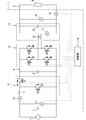
- FIG. 1 is an example of a circuit diagram of a power converter.
- a power conversion device 1 is provided between a DC power source 2 and an AC circuit 3, and in a state where the DC voltage of the DC power source 2 is lower than the peak value (peak value) of the AC voltage of the AC circuit 3. Perform AC power conversion.
- the power converter 1 can supply, for example, AC power generated based on the DC power source 2 to the load 4 connected to the AC circuit 3 as an independent output.
- the power converter 1 includes a direct-current side capacitor 5, a DC / DC converter 6, an intermediate capacitor 9, an inverter 10, and a filter circuit 11 as main circuit components.
- the DC / DC converter 6 includes a DC reactor 7, a high-side switching element Q1, and a low-side switching element Q2, and constitutes a DC chopper circuit.
- the switching elements Q1 and Q2 for example, MOSFET (Metal-Oxide-Semiconductor Field Effect Transistor) can be used.
- the MOSFET switching elements Q1, Q2 have diodes (body diodes) d1, d2, respectively. Each switching element Q1, Q2 is controlled by the control unit 14.
- the high voltage side of the DC / DC converter 6 is connected to the DC bus 8.
- the intermediate capacitor 9 connected between the two lines of the DC bus 8 has a small capacity (100 ⁇ F or less, for example, several tens of ⁇ F), and exhibits a smoothing action for a voltage switched at a high frequency (for example, 20 kHz). However, it does not exert a smoothing action on a voltage that changes at a frequency (100 Hz or 120 Hz) that is about twice the commercial frequency.
- the inverter 10 connected to the DC bus 8 includes switching elements Q3 to Q6 that constitute a full bridge circuit.
- These switching elements Q3 to Q6 are, for example, MOSFETs.
- the switching elements Q3 to Q6 have diodes (body diodes) d3 to d6, respectively.
- the switching elements Q3 to Q6 are controlled by the control unit 14.
- a filter circuit 11 is provided between the inverter 10 and the AC circuit 3.
- the filter circuit 11 includes an AC reactor 12 and an AC capacitor 13 provided on the load 4 side (right side in the figure) from the AC reactor 12.
- the filter circuit 11 prevents passage of high-frequency noise generated in the inverter 10 so as not to leak to the AC electric circuit 3 side.
- a voltage sensor 15 and a current sensor 16 are provided on the low voltage side (left side in the figure) of the DC / DC converter 6.
- the voltage sensor 15 is connected in parallel with the DC power supply 2 and detects the voltage across the DC power supply 2. Information on the detected voltage is provided to the control unit 14.
- the current sensor 16 detects a current flowing through the DC / DC converter 6. Information on the detected current is provided to the control unit 14.
- a current sensor 17 for detecting a current flowing through the AC reactor 12 is provided on the AC side. Information on the current detected by the current sensor 17 is provided to the control unit 14.
- a voltage sensor 18 is provided in parallel with the AC capacitor 13.
- the current sensor 19 is provided in the electric circuit that connects the load 4 and the power conversion device 1. Information on the voltage detected by the voltage sensor 18 and information on the current detected by the current sensor 19 are respectively provided to the control unit 14.
- the control unit 14 includes, for example, a computer, and a necessary control function is realized by the computer executing a software (computer program).
- the software is stored in a storage device (not shown) of the control unit 14.
- the said power converter device 1 performs only conversion from direct current
- the power conversion device 1 can charge the storage battery by performing conversion from AC to DC in addition to conversion from DC to AC. That is, the inverter 10 and the DC / DC converter 6 can each perform an operation of sending power in both directions.
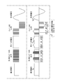
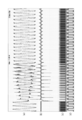
- FIG. 2 and FIG. 3 are waveform diagrams simply showing the characteristics of the operation of the DC / DC converter 6 and the inverter 10 in the minimum switching conversion method. Although both figures show the same contents, FIG. 2 particularly displays the amplitude relationship from the DC input to the AC output so that it can be easily seen, and FIG. 3 particularly shows the control timing so that it can be easily seen.
- the upper part of FIG. 2 and the left column of FIG. 3 are waveform diagrams representing traditional switching control that is not the minimum switching conversion method, for comparison.
- 2 and the right column of FIG. 3 are waveform diagrams showing the operation of the minimum switching conversion method.
- the output at the interconnection point of the pair of switching elements of the DC / DC converter and the DC reactor with respect to the input DC voltage is It is in the form of an equidistant pulse train having a value higher than the DC voltage.
- This output is smoothed by an intermediate capacitor and appears as a voltage on the DC bus.
- the inverter performs PWM (Pulse Width Modulation) controlled switching while inverting the polarity in a half cycle. As a result, a sinusoidal AC voltage is obtained through final smoothing.
- PWM Pulse Width Modulation
- V ac * is a voltage target value at the AC output terminal of the inverter 10 in consideration of the influence of the filter circuit 11 on the current / voltage.
- V dc is a value that takes into account the voltage drop due to the DC reactor 7 to the voltage across the DC power supply 2.
- the intermediate capacitor 9 has a small capacity, a part of the waveform around the peak of the absolute value of the AC waveform remains without being smoothed. That is, the smoothing works to the extent that the trace of the high frequency switching by the DC / DC converter 6 is erased, but the intermediate capacitor 9 has a small capacity so that the low frequency about twice the commercial frequency cannot be smoothed. It has become.
- the inverter 10
- High-frequency switching is performed (“OP” in the figure), and when
- the inverter 10 When the high frequency switching is stopped, the inverter 10 has the switching elements Q3 and Q6 on, Q4 and Q5 off (non-inverted), the switching elements Q3 and Q6 off and Q4 and Q5 on ( By selecting one of (inversion), only necessary polarity inversion is performed.
- the output of the inverter 10 is smoothed by the AC reactor 12 and the AC side capacitor 13, and a desired AC output is obtained.
- the DC / DC converter 6 and the inverter 10 are alternately performing high-frequency switching operation, and when the DC / DC converter 6 is performing a boosting operation, The inverter 10 stops high-frequency switching and performs only necessary polarity inversion with respect to the voltage of the DC bus 8. Conversely, when the inverter 10 performs a high frequency switching operation, the DC / DC converter 6 stops and a voltage based on the voltage across the DC capacitor 5 appears on the DC bus 8 via the DC reactor 7 and the diode d1.
- Such a power conversion device 1 can reduce the overall number of high-frequency switching operations by generating a pause in the high-frequency switching of the switching elements Q1 to Q6. Thereby, the efficiency of power conversion can be improved significantly.
- FIG. 4 is a diagram illustrating a capacitor input rectifier circuit as an example of a non-linear load.
- the capacitor input type rectifier circuit 4d an AC voltage is input to the diode bridge 4b via the resistor 4a.
- a capacitor 4c is connected in parallel to the DC output side of the diode bridge 4b.
- a DC load 4e is connected to the capacitor input type rectifier circuit 4d.
- the capacitor 4c having a charge of 0 or in the vicinity of 0 is in a state close to a short circuit with respect to the applied voltage, and therefore the inrush current becomes a large current.
- the peak value of the inrush current depends on the resistance value of the closed circuit constituted by the diode bridge 4b and the capacitor 4c.
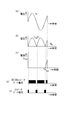
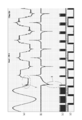
- FIG. 5 shows a voltage when a non-linear load such as the capacitor input type rectifier circuit 4d is connected as the load 4 of the power conversion device 1 in FIG. • It is a current waveform diagram.
- (a) is the output voltage V a ( ⁇ V ac * ) detected by the voltage sensor 18 in FIG. (B) has shown the absolute value of voltage target value Vac * used as the basis of the output voltage of (a), and DC voltage Vdc .
- (C) is an output current detected by the current sensor 17 or the current sensor 19.
- (D) shows the gate voltage (gate-source voltage) of the switching element Q2 on the low side of the DC / DC converter 6 (switching during boosting).
- (E) shows the gate voltage of the switching element Q3 (switching at the time of step-down) of the inverter 10, for example.
- the boosting by the DC / DC converter 6 and the inverter 10 are performed according to the comparison between the absolute value of the voltage target value V ac * of the AC voltage and the DC voltage V dc. Step-down is performed alternately.
- a non-linear load 4 (4d) is connected at time ts when the voltages of (a) and (b) become zero cross, an inrush current flows and the output voltage rises as shown in (c). Along with it suddenly becomes a large value.
- the control unit 14 gate-blocks both the DC / DC converter 6 and the inverter 10, The conversion device 1 stops. If this happens, it will be necessary to reset and restart, and if a person does it, a long time outage is also expected. Moreover, even if automatic reset and restart after a certain time, a certain operation stop time occurs.
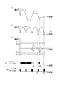
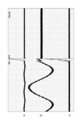
- FIG. 6 shows, as an embodiment of the present invention, voltage / current waveforms when a non-linear load such as the capacitor input rectifier circuit 4d is connected as the load 4 of the power converter 1 in FIG. FIG.
- (a) shows the output voltage V a detected by the voltage sensor 18 in Figure 1.
- (B) shows the absolute value of the voltage target value V ac * and the DC voltage V dc .
- (C) is an output current detected by the current sensor 17 or the current sensor 19.
- D) shows the gate voltage (gate-source voltage) of the switching element Q2 on the low side of the DC / DC converter 6 (switching during boosting).
- E shows the gate voltage of the switching element Q3 (switching at the time of step-down) of the inverter 10, for example.
- Boosted by the switching element Q2 of the converter 6 is gated block is immediately stopped, the output voltage V a is dropped to the level of the DC voltage V dc (a), the end of the switching period of the DC / DC converter 6 This state is maintained until time t2. After time t2, the inverter 10 operates and the AC waveform is partially restored.
- the control unit 14 releases the gate block for the switching element Q2 of the DC / DC converter 6.
- boosting by the DC / DC converter 6 can be performed again in the (1/2) cycle from the next zero cross.
- the direction of the output current changes in the AC half cycle after time t3 of the zero cross. Also, the output current suddenly becomes a large value again as the output voltage increases in the negative direction.
- the control unit 14 performs DC / DC
- the switching element Q2 of the converter 6 is gate-blocked. However, the control unit 14 does not block the inverter 10.
- Boosted by the switching element Q2 of the converter 6 is gated block is immediately stopped, the output voltage V a is dropped to sign inversion level of the DC voltage V dc, as shown in (a) (-V dc), DC / DC This state is maintained until the end time t5 of the switching period of the converter 6. After time t5, the inverter 10 operates and the AC waveform is partially restored.
- the gate block and the subsequent release of the DC / DC converter 6 as described above are performed every AC half cycle while the output current reaches the converter gate block threshold value I th_b or ⁇ I th_b after time t6 of the next zero crossing. Repeatedly. Thus, the gate block and the subsequent release can be repeated as many times as necessary until the output current to the load 4 does not reach the converter gate block threshold.
- the control unit 14 performs the normal minimum switching control.
- the load to be used is the load 4 including the capacitor input type rectifier circuit 4d of FIG. 4, and the non-linear load test of “JIS C 4411-3: 2014 Uninterruptible Power Supply (UPS) —Part 3: Performance and Test Requirements”
- the circuit constant determination method specified in is adopted.
- the apparent power of the non-linear load was set to 500 VA
- the resistance value of the resistor 4a was 0.8 ⁇
- the capacitance of the capacitor 4c was 2750 ⁇ F
- the resistance value of the DC load 4e was 45.1 ⁇ .
- the voltage of the DC power supply 2 is 43V, and the power conversion device 1 performs a self-sustained output operation of AC 101V output.
- the converter gate block threshold I th_b for gate blocking the DC / DC converter 6 was set to 23.5 A, and the instantaneous overcurrent protection threshold I th_p was set to 80 A.
- FIG. 7 is a waveform diagram of voltages and currents from the moment the nonlinear load is connected to the steady state in the power conversion device 1 that takes measures against inrush current by the gate block. 7, (a) is the output voltage, (b) is the output current, (c) is the gate voltage of the switching element Q2 of the DC / DC converter 6, and (d) is the gate voltage of the switching element Q3 of the inverter 10. .
- FIG. 8 is an enlarged view of the time axis when the nonlinear load is connected in FIG.
- FIG. 9 is an enlarged view of the time axis at the time when the steady state in FIG. 7 is reached.
- the gate block of the DC / DC converter 6 is performed at the moment when the output current of (b) reaches the converter gate block threshold value (I th — b) as shown in the X part.
- the output voltage in (a) does not maintain a sine wave shape, so that the increase in voltage stops and power conversion is performed without increasing the output current up to the instantaneous overcurrent protection threshold (I th — p ). It can be seen that the operation of the device 1 can be continued.
- the peak value in the output current of (b) becomes small, and the latter half has reached a steady state.
- 4 is an effective value obtained by smoothing the pulsating flow that has been full-wave rectified by the diode bridge 4b, the ripple in the vicinity of the peak value of the pulsating flow continues even in the steady state.
- the gate voltage of the DC / DC converter 6 shown in (c) the gate block is not performed in the latter half, and the inverter 10 shown in (d) is switched alternately while resting to perform the operation of the minimum switching method. You can see that
- FIG. 10 is also a voltage / current waveform diagram from the moment when the nonlinear load is connected until the steady state is reached.
- (A) is the output voltage
- (b) is the output current
- (c) is the voltage across the load 4. In this figure, it can be seen that the voltage across the load 4 gradually increases until it reaches a steady state.
- the voltage is boosted by the DC / DC converter 6 within one AC cycle, the inverter 10 stops the high-frequency switching, and the inverter 10 The voltage is stepped down, and the DC / DC converter 6 is controlled such that the time when the high frequency switching is stopped alternately appears.
- the waveform of the AC voltage to be generated is a composite waveform output by the DC / DC converter and the inverter operating alternately.
- the waveform region having a relatively large absolute value before and after the peak value is generated by the DC / DC converter 6.
- the inverter 10 generates a waveform region that is generated and has a relatively small absolute value before and after the zero crossing.
- the power conversion device 1 can suppress the inrush current without stopping the operation due to the instantaneous overcurrent protection.
- the output current measurement for the gate block can be performed by either the current sensor 17 or the current sensor 19.
- the current sensor 17 is provided because it is necessary for the control of the minimum switching conversion method. Therefore, the current sensor 19 can be omitted.
- the current sensor 17 is connected in series with the AC reactor 12 without anything, it is difficult to detect a sudden change in current due to the influence of the AC reactor 12. In that respect, when the current sensor 19 is provided between the load 4 and the AC side capacitor 13 and is provided in series with the load 4, the rapid change of the current flowing through the load 4 is captured with better response. There is an advantage that can be.
- a capacitor input type rectifier circuit is used as the load 4 of the power converter 1.
- the same current suppression by the gate block is effective for the starting current of an inductive load such as a motor. .
Landscapes
- Engineering & Computer Science (AREA)
- Power Engineering (AREA)
- Inverter Devices (AREA)
Abstract
Priority Applications (4)
| Application Number | Priority Date | Filing Date | Title |
|---|---|---|---|
| CN201680083834.0A CN109104890B (zh) | 2016-03-24 | 2016-10-24 | 电力转换装置以及用于控制电力转换装置的方法 |
| US16/084,419 US10340814B2 (en) | 2016-03-24 | 2016-10-24 | Gate-blocking a DC/DC converter based upon output current of an AC reactor in a power conversion device |
| KR1020187026288A KR102497621B1 (ko) | 2016-03-24 | 2016-10-24 | 전력 변환 장치 및 그 제어 방법 |
| EP16895496.4A EP3435534B1 (fr) | 2016-03-24 | 2016-10-24 | Dispositif de conversion de puissance et son procédé de commande |
Applications Claiming Priority (2)
| Application Number | Priority Date | Filing Date | Title |
|---|---|---|---|
| JP2016-060067 | 2016-03-24 | ||
| JP2016060067A JP6620629B2 (ja) | 2016-03-24 | 2016-03-24 | 電力変換装置及びその制御方法 |
Publications (1)
| Publication Number | Publication Date |
|---|---|
| WO2017163473A1 true WO2017163473A1 (fr) | 2017-09-28 |
Family
ID=59901088
Family Applications (1)
| Application Number | Title | Priority Date | Filing Date |
|---|---|---|---|
| PCT/JP2016/081441 WO2017163473A1 (fr) | 2016-03-24 | 2016-10-24 | Dispositif de conversion de puissance et son procédé de commande |
Country Status (6)
| Country | Link |
|---|---|
| US (1) | US10340814B2 (fr) |
| EP (1) | EP3435534B1 (fr) |
| JP (1) | JP6620629B2 (fr) |
| KR (1) | KR102497621B1 (fr) |
| CN (1) | CN109104890B (fr) |
| WO (1) | WO2017163473A1 (fr) |
Families Citing this family (2)
| Publication number | Priority date | Publication date | Assignee | Title |
|---|---|---|---|---|
| KR102343688B1 (ko) * | 2016-12-09 | 2021-12-27 | 삼성에스디아이 주식회사 | 전력 변환 장치 및 이를 포함하는 무정전 전원 공급 장치 |
| WO2021033267A1 (fr) * | 2019-08-20 | 2021-02-25 | 東芝三菱電機産業システム株式会社 | Dispositif de conversion de puissance |
Citations (4)
| Publication number | Priority date | Publication date | Assignee | Title |
|---|---|---|---|---|
| JPH01318543A (ja) * | 1988-06-17 | 1989-12-25 | Sony Tektronix Corp | 直流・直流変換型電源回路 |
| JP2000295839A (ja) * | 1999-04-06 | 2000-10-20 | Mitsubishi Electric Corp | 電源装置 |
| JP2000333473A (ja) * | 1999-05-24 | 2000-11-30 | Matsushita Electric Ind Co Ltd | 系統連系インバータ装置 |
| JP2003067065A (ja) * | 2001-08-28 | 2003-03-07 | Matsushita Electric Ind Co Ltd | バッテリ内蔵型電力変換装置 |
Family Cites Families (9)
| Publication number | Priority date | Publication date | Assignee | Title |
|---|---|---|---|---|
| US2545987A (en) * | 1947-02-25 | 1951-03-20 | Westinghouse Electric Corp | Protective relay for transmission lines |
| JPS57142177A (en) * | 1981-02-24 | 1982-09-02 | Toshiba Corp | Control system for inverter device |
| GB2415841B (en) * | 2004-11-08 | 2006-05-10 | Enecsys Ltd | Power conditioning unit |
| JP5134263B2 (ja) | 2007-03-01 | 2013-01-30 | 本田技研工業株式会社 | 電力変換装置 |
| JP5817767B2 (ja) | 2013-03-21 | 2015-11-18 | トヨタ自動車株式会社 | 電気自動車 |
| JP5618022B1 (ja) | 2013-06-11 | 2014-11-05 | 住友電気工業株式会社 | インバータ装置 |
| JP6379553B2 (ja) * | 2014-03-20 | 2018-08-29 | 住友電気工業株式会社 | 変換装置 |
| WO2015182669A1 (fr) * | 2014-05-29 | 2015-12-03 | カルソニックカンセイ株式会社 | Circuit d'attaque pour élément de commutation à semi-conducteur |
| DE102016120033A1 (de) * | 2016-10-20 | 2018-04-26 | Ge Energy Power Conversion Technology Limited | Verfahren zur Steuerung eines Photovoltaik-Wechselrichters zum Durchfahren eines Netzfehlers und Photovoltaik-Wechselrichtersystem |
-
2016
- 2016-03-24 JP JP2016060067A patent/JP6620629B2/ja active Active
- 2016-10-24 US US16/084,419 patent/US10340814B2/en active Active
- 2016-10-24 WO PCT/JP2016/081441 patent/WO2017163473A1/fr active Application Filing
- 2016-10-24 CN CN201680083834.0A patent/CN109104890B/zh active Active
- 2016-10-24 KR KR1020187026288A patent/KR102497621B1/ko active IP Right Grant
- 2016-10-24 EP EP16895496.4A patent/EP3435534B1/fr active Active
Patent Citations (4)
| Publication number | Priority date | Publication date | Assignee | Title |
|---|---|---|---|---|
| JPH01318543A (ja) * | 1988-06-17 | 1989-12-25 | Sony Tektronix Corp | 直流・直流変換型電源回路 |
| JP2000295839A (ja) * | 1999-04-06 | 2000-10-20 | Mitsubishi Electric Corp | 電源装置 |
| JP2000333473A (ja) * | 1999-05-24 | 2000-11-30 | Matsushita Electric Ind Co Ltd | 系統連系インバータ装置 |
| JP2003067065A (ja) * | 2001-08-28 | 2003-03-07 | Matsushita Electric Ind Co Ltd | バッテリ内蔵型電力変換装置 |
Non-Patent Citations (1)
| Title |
|---|
| See also references of EP3435534A4 * |
Also Published As
| Publication number | Publication date |
|---|---|
| CN109104890A (zh) | 2018-12-28 |
| EP3435534A1 (fr) | 2019-01-30 |
| US10340814B2 (en) | 2019-07-02 |
| EP3435534A4 (fr) | 2019-11-13 |
| KR20180125959A (ko) | 2018-11-26 |
| CN109104890B (zh) | 2020-11-13 |
| JP6620629B2 (ja) | 2019-12-18 |
| JP2017175797A (ja) | 2017-09-28 |
| US20190081575A1 (en) | 2019-03-14 |
| KR102497621B1 (ko) | 2023-02-07 |
| EP3435534B1 (fr) | 2020-10-07 |
Similar Documents
| Publication | Publication Date | Title |
|---|---|---|
| US10530238B2 (en) | Power conversion device and method for controlling same | |
| JP3695382B2 (ja) | 電力供給装置、電動機駆動装置、電力供給装置の制御方法 | |
| JP5928647B2 (ja) | 電力変換装置 | |
| JP6038293B2 (ja) | 電力変換装置 | |
| WO2018012146A1 (fr) | Dispositif de conversion de puissance et procédé de commande de dispositif de conversion de puissance | |
| JP5678860B2 (ja) | 交流直流変換器 | |
| JP6349974B2 (ja) | 変換装置 | |
| TW201711367A (zh) | 轉換裝置及其控制方法 | |
| WO2017163473A1 (fr) | Dispositif de conversion de puissance et son procédé de commande | |
| JP5439989B2 (ja) | 電力制御装置および電力制御装置における電力算出方法 | |
| JP6591092B2 (ja) | コンバータ装置、モータ駆動装置、冷蔵庫、空気調和装置及びヒートポンプ給湯装置 | |
| JP2000188867A (ja) | コンバータ回路および直流電圧制御用装置 | |
| JP6907740B2 (ja) | 電力変換装置及びその制御方法 | |
| KR101946369B1 (ko) | 전력 변환 장치 및 이를 포함하는 공기 조화기 | |
| JP2017184450A (ja) | 電力変換装置並びに蓄電池の充電制御方法及び放電制御方法 | |
| JP6707980B2 (ja) | 電力変換装置 | |
| JP2011155767A (ja) | 電源装置 | |
| JP2019146372A (ja) | 電力変換装置、電源システム、及び、電力変換装置の制御方法 | |
| JP2020010429A (ja) | 電力変換装置、電源装置、及び、電力変換装置の直流成分抑制方法 | |
| KR20180091193A (ko) | 전력 변환 장치 및 이를 포함하는 공기 조화기 | |
| JP2012244672A (ja) | 電源装置 |
Legal Events
| Date | Code | Title | Description |
|---|---|---|---|
| ENP | Entry into the national phase |
Ref document number: 20187026288 Country of ref document: KR Kind code of ref document: A |
|
| NENP | Non-entry into the national phase |
Ref country code: DE |
|
| WWE | Wipo information: entry into national phase |
Ref document number: 2016895496 Country of ref document: EP |
|
| ENP | Entry into the national phase |
Ref document number: 2016895496 Country of ref document: EP Effective date: 20181024 |
|
| 121 | Ep: the epo has been informed by wipo that ep was designated in this application |
Ref document number: 16895496 Country of ref document: EP Kind code of ref document: A1 |