WO2017159072A1 - Dispositif de commande de moteur et système d'entraînement - Google Patents
Dispositif de commande de moteur et système d'entraînement Download PDFInfo
- Publication number
- WO2017159072A1 WO2017159072A1 PCT/JP2017/003085 JP2017003085W WO2017159072A1 WO 2017159072 A1 WO2017159072 A1 WO 2017159072A1 JP 2017003085 W JP2017003085 W JP 2017003085W WO 2017159072 A1 WO2017159072 A1 WO 2017159072A1
- Authority
- WO
- WIPO (PCT)
- Prior art keywords
- phase
- voltage
- correction
- control device
- motor control
- Prior art date
Links
Images


Classifications
-
- H—ELECTRICITY
- H02—GENERATION; CONVERSION OR DISTRIBUTION OF ELECTRIC POWER
- H02P—CONTROL OR REGULATION OF ELECTRIC MOTORS, ELECTRIC GENERATORS OR DYNAMO-ELECTRIC CONVERTERS; CONTROLLING TRANSFORMERS, REACTORS OR CHOKE COILS
- H02P27/00—Arrangements or methods for the control of AC motors characterised by the kind of supply voltage
- H02P27/04—Arrangements or methods for the control of AC motors characterised by the kind of supply voltage using variable-frequency supply voltage, e.g. inverter or converter supply voltage
- H02P27/06—Arrangements or methods for the control of AC motors characterised by the kind of supply voltage using variable-frequency supply voltage, e.g. inverter or converter supply voltage using dc to ac converters or inverters
- H02P27/08—Arrangements or methods for the control of AC motors characterised by the kind of supply voltage using variable-frequency supply voltage, e.g. inverter or converter supply voltage using dc to ac converters or inverters with pulse width modulation
-
- H—ELECTRICITY
- H02—GENERATION; CONVERSION OR DISTRIBUTION OF ELECTRIC POWER
- H02P—CONTROL OR REGULATION OF ELECTRIC MOTORS, ELECTRIC GENERATORS OR DYNAMO-ELECTRIC CONVERTERS; CONTROLLING TRANSFORMERS, REACTORS OR CHOKE COILS
- H02P21/00—Arrangements or methods for the control of electric machines by vector control, e.g. by control of field orientation
-
- H—ELECTRICITY
- H02—GENERATION; CONVERSION OR DISTRIBUTION OF ELECTRIC POWER
- H02P—CONTROL OR REGULATION OF ELECTRIC MOTORS, ELECTRIC GENERATORS OR DYNAMO-ELECTRIC CONVERTERS; CONTROLLING TRANSFORMERS, REACTORS OR CHOKE COILS
- H02P27/00—Arrangements or methods for the control of AC motors characterised by the kind of supply voltage
- H02P27/04—Arrangements or methods for the control of AC motors characterised by the kind of supply voltage using variable-frequency supply voltage, e.g. inverter or converter supply voltage
-
- H—ELECTRICITY
- H02—GENERATION; CONVERSION OR DISTRIBUTION OF ELECTRIC POWER
- H02P—CONTROL OR REGULATION OF ELECTRIC MOTORS, ELECTRIC GENERATORS OR DYNAMO-ELECTRIC CONVERTERS; CONTROLLING TRANSFORMERS, REACTORS OR CHOKE COILS
- H02P2209/00—Indexing scheme relating to controlling arrangements characterised by the waveform of the supplied voltage or current
- H02P2209/09—PWM with fixed limited number of pulses per period
Definitions
- the present invention relates to a motor control device and a drive system for reducing harmonic loss.
- the loss is divided into a loss generated in the motor (hereinafter referred to as motor loss) and a loss generated in the inverter (hereinafter referred to as inverter loss).
- the motor loss includes a loss due to the fundamental component (hereinafter referred to as fundamental loss) and a loss due to the harmonic component (hereinafter referred to as harmonic loss).
- the inverter loss includes a loss caused by the on / off operation of the switching element (hereinafter referred to as switching loss) and a loss generated when the switching element is conducted (hereinafter referred to as conduction loss).
- ⁇ Fundamental loss is reduced by adopting variable speed drive by inverter compared to constant speed drive by commercial power supply.
- the voltage and current are distorted by the switching operation, and harmonic components are generated, so that harmonic loss increases.
- Harmonic components and harmonic losses can be reduced by improving the carrier frequency of the inverter.
- switching loss increases at the same time, it is desirable to reduce harmonic loss without increasing the carrier frequency.
- harmonic components and harmonic loss are remarkably increased, and reduction thereof is desired.
- Patent Document 1 is a technology for synchronous PWM control for railways.
- the pulse voltage is near the zero cross point (0,180 deg) and peak point (90,270 deg) of the fundamental phase. It is turned on or off once or more, and is kept on or off in other phase regions.
- Patent Document 1 The problem of Patent Document 1 is the method for synchronous PWM control, so it does not support asynchronous PWM control, and because it is for railways, the upper limit of the carrier frequency is low, and it is only in a narrow drive range. The effect does not appear.
- an object of the present invention is to reduce or minimize harmonic loss generated when an AC motor is driven in an overmodulation region.
- the present invention switches the final correction signal wave from 0 to the synchronization correction signal when the modulation rate reaches a predetermined value of 1 or more, and the modulation rate is 1 or more.
- the predetermined value is reached, the final amplitude is switched from the first amplitude to the fixed amplitude.
- harmonic loss generated when an AC motor is driven in an overmodulation region using an inverter can be reduced.
- effects such as higher output of the AC motor or downsizing of the cooling system can be obtained.
- Example 1 will be described with reference to FIGS. 1 to 14 and FIG.
- Fig. 1 is a block diagram of the motor control device in the first embodiment, and Fig. 2 shows its elements.
- the inverter 2 can control the AC motor 1 by converting the DC voltage VDC into an arbitrary frequency.
- AC motor 1 is applied with a three-phase AC current (U-phase current Iu, V-phase current Iv, W-phase) by applying a pulse voltage (U-phase pulse voltage Vu, V-phase pulse voltage Vv, W-phase pulse voltage Vw).
- the current Iw flows and is driven at the drive frequency f.
- line voltage Vuv the voltage applied between the U-V phases of AC motor 1 is referred to as line voltage Vuv.
- the frequency calculation unit 3 calculates the carrier frequency fc * and the base number B based on the fundamental frequency f1 *.
- the base number B is the ratio of the carrier frequency fc * and the fundamental frequency f1 *.
- the frequency correction unit 4 calculates the correction carrier frequency fc2 * based on the base number B and the pattern P.
- the first modulation mode determination unit 5 switches the final carrier frequency fc2 ** from the carrier frequency fc * to the corrected carrier frequency fc2 * when the modulation factor Kh * reaches a predetermined value of 1 or more.
- the carrier wave generator 6 outputs a carrier wave Vc * based on the final carrier frequency fc **.
- the carrier wave Vc * is a triangular wave having an amplitude of 1 (normalized by the DC voltage VDC / 2) as shown in FIG. 3, and is a function depending on the voltage phase ⁇ *.
- the amplitude calculator 7 calculates the first amplitude Amp1 based on the modulation factor Kh *.
- the second modulation mode determination unit 8 switches the final amplitude Amp from the first amplitude Amp1 to the fixed amplitude Amp2 when the modulation factor Kh * reaches a predetermined value of 1 or more.
- the signal wave generator 9 outputs a signal wave (U phase signal wave Vu *, V phase signal wave Vv *, W phase signal wave Vw *) based on the voltage phase ⁇ * and the final amplitude Amp.
- the signal wave Vu * is a sine wave as shown in FIG. 3, and is a function depending on the voltage phase ⁇ *.
- the correction amount calculation unit 10 calculates the pulse number Pn, the zero cross correction amount A1, and the peak correction amount Am based on the modulation factor Kh *, the voltage phase ⁇ *, and the base number B.
- the pattern determination unit 11 determines the pattern P based on the number of bases. Here, when the pattern P is 1, it is the first pattern, and when P is 2, it is the second pattern.
- the synchronization correction phase calculation unit 12 calculates the zero hold phase ⁇ 0, the zero cross phase ⁇ 1, and the peak phase ⁇ 2 based on the number of pulses Pn, the pattern P, the correction carrier frequency fc2 *, and the fundamental frequency f1 *.
- the zero holding phase ⁇ 0 is a phase corresponding to a quarter period of the carrier wave Vc *.
- the correction signal generator 13 generates the synchronization correction signal A based on the zero hold phase ⁇ 0, the zero cross phase ⁇ 1, the peak phase ⁇ 2, the zero cross correction amount A1, the peak correction amount Am, and the voltage phase ⁇ *.
- the synchronization correction signal A is a function that depends on the voltage phase ⁇ *.
- the third modulation mode determination unit 14 switches the final correction signal A * from 0 to the synchronization correction signal A when the modulation factor Kh * reaches a predetermined value of 1 or more.
- the PWM controller 15 compares the correction signal waves Vu2 *, Vv2 *, Vw2 * and the carrier wave Vc * obtained by adding the final correction signal A * to the signal waves Vu *, Vv *, Vw *,
- the gate signals Gun, Gup, Gvn, Gvp, Gwn, Gwv are generated and output to the inverter 2.
- the inverter 2 turns on or off the switching element based on the gate signals Gun, Gup, Gvn, Gvp, Gwn, Gwv, and applies the pulse voltages Vu, Vv, Vw to the AC motor 1.
- FIG. 2 is a block diagram element of the correction amount calculation unit 10.
- the control angle calculation unit 10a calculates the control angle ⁇ and the pulse number Pn based on the modulation rate Kh * and the base number B.
- the peak correction amount calculation unit 10b calculates the peak correction amount Am based on the modulation rate.
- the zero cross correction amount calculation unit 10c calculates the zero cross correction amount A1 based on the number of pulses Pn and the modulation rate Kh *.
- the PWM control unit 15 acquires the values of the signal waves Vu *, Vv *, Vw * every half cycle of the carrier wave Vc *, and compares them with the carrier wave Vc * to obtain the gate signals Gun, Gup, Gvn, Gvp. , Gwn, Gwv high or low.
- the inverter 2 outputs pulse voltages Vu, Vv, Vw to the AC motor 1 in accordance with the high or low of the gate signals Gun, Gup, Gvn, Gvp, Gwn, Gwv.
- the gate signal Gup is high, Gun is low, and the pulse voltage Vu is turned on.
- PWM control includes synchronous PWM control and asynchronous PWM control.
- Example 1 describes synchronous PWM control.
- the carrier frequency fc * is calculated by the frequency calculation unit 3 to be an integral multiple of the fundamental frequency f1 *, and the pulse voltage Vu is calculated with respect to the period T1 of the signal waves Vu *, Vv *, and Vw *.
- the carrier frequency fc * is calculated so as to satisfy (Equation 1) in order to keep the pulse voltages Vu, Vv, and Vw symmetrical.
- Pn is the number of pulses of the pulse voltages Vu, Vv, Vw per fundamental wave cycle.
- the pulse number Pn of the pulse pattern shown in FIG. 3 (a) is 9 pulses.
- F cmax is the maximum carrier frequency at which synchronous PWM control is possible.
- the maximum carrier frequency fc of a railway inverter is about several hundred Hz
- the maximum carrier frequency fcmax of a general-purpose inverter is about several kHz.
- Asynchronous PWM control is used when PWM control is performed at a carrier frequency fc * higher than the maximum carrier frequency fcmax. The above is the operating principle of PWM control.
- the harmonic loss Wh which is a problem with PWM control, will be described.
- PWM control distortion occurs in the voltage and current as the switching element of the inverter 2 is turned on or off. This distortion can be expressed as a harmonic component shown in FIG. 2 (b), which generates a harmonic loss Wh.
- the overmodulation region is a region where the modulation factor Kh * exceeds 1 (p.u.), and a region where the modulation factor Kh * is less than 1 (p.u.) is called a modulation region.
- the number of pulses Pn (7 pulses) in the overmodulation region is smaller than the number of pulses Pn (9 pulses) in the modulation region.
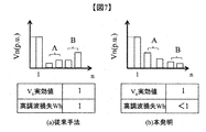
- the effective value of the harmonic voltage Vn increases and the harmonic loss Wh also increases. For example, as shown in Fig.
- the effective value of the 13th harmonic voltage Vn is 0.008 p.u. when the motor is driven in the modulation range.
- the effective value is 0.291 p.u, which is approximately 30 times that of the motor driven in the modulation range.
- the harmonic voltage Vn is an effective value of the harmonic component determined by the pulse pattern, and a phase ⁇ (hereinafter referred to as a control angle ⁇ ) in which the pulse voltage Vu, Vv, Vw switches from on to off or from off to on. ) And is expressed as (Equation 2).
- the modulation factor Kh * depends on the control angle ⁇ and is expressed as (Equation 3).
- FIG. 5 shows the waveform diagram of the third harmonic superposition method.
- the first amplitude Amp1 of the signal waves Vu *, Vv *, Vw * in the third-order harmonic superposition method is calculated as (Equation 4) based on the modulation rate Kh *.
- the modulation factor Kh * 1.15
- the difference from the amplitude of the carrier wave Vc * is 0.15 pu. It becomes. Therefore, in the third harmonic superposition method, the effective value of the harmonic voltage Vn in the overmodulation region is reduced compared to the sine wave method.
- the harmonic loss Wh is the sum of the eddy current generated in the magnet of the AC motor 1 and the hysteresis loss generated in the electromagnetic steel sheet, and is proportional to the square of the harmonic current In.
- the harmonic current In can be expressed as (Equation 5) using the harmonic voltage Vn of (Equation 2).
- the loss coefficient ⁇ is a coefficient representing the characteristic of the harmonic loss Wh of the AC motor 1, and is determined as follows depending on the factor (FIG. 20) of the harmonic loss Wh of the AC motor 1.
- the loss factor ⁇ is between 0 and 2.
- the loss coefficient ⁇ is 0 ⁇ ⁇ ⁇ 1.
- the harmonic loss Wh does not have frequency dependence, so the harmonic current In and the harmonic loss Wh are in a proportional relationship. Therefore, by reducing the harmonic voltage Vn, the harmonic current In is also reduced, and as a result, the harmonic loss Wh is reduced.
- the harmonic loss Wh is frequency-dependent, the loss coefficient ⁇ is larger than 0, and therefore the harmonic resistance n ⁇ and the harmonic order n have the relationship shown in FIG. That is, the higher the harmonic order n, the higher the harmonic resistance n ⁇ . Therefore, the higher harmonic voltage Vn than the lower harmonic voltage Vn affects the harmonic loss Wh. Therefore, the harmonic loss Wh is greatly reduced by reducing the higher-order harmonic voltage Vn shown in B of FIG. 7 even if the increase of the lower-order harmonic voltage Vn shown in A of FIG. 7 is allowed. can do. That is, it is necessary to reduce the effective value of the higher-order harmonic voltage Vn in accordance with the loss factor ⁇ .
- Equation 7 In order to determine the pulse pattern in consideration of the frequency dependence of the harmonic loss Wh, (Equation 7) is used as the optimization objective function, and the control angle ⁇ is calculated so as to reduce or minimize this.
- the modulation factor Kh * is influenced by the control angle ⁇ , and is therefore a constraint condition for optimization.
- the modulation factor Kh * which is a constraint condition, is fixed at 1.2.
- There is a pattern that turns off at the phase ⁇ * 0 deg.
- the former is referred to as a first pattern, and the latter is referred to as a second pattern.
- the frequency correction unit 4, the correction amount calculation unit 10, the synchronization correction phase calculation unit 12, and the correction signal generation unit 13 are used to generate the synchronization correction signal A, and the above features (a) to (d)
- the pulse pattern that holds the constraints (A) and (B) is output to the inverter 2. The principle will be described below.
- the frequency correction unit 4 calculates a correction signal fc2 * that satisfies the constraints of (Equation 8) or (Equation 9) and (Equation 10), (Equation 1) based on the base number B and the pattern P.
- the pulse voltage Vu holds (b)-(d) while satisfying the constraints (A) and (B).
- the zero retention phase ⁇ 0 is calculated based on (Equation 11).
- the correction base number B2 is a ratio of the correction carrier frequency fc2 * and the fundamental frequency f1 *.
- the zero cross phase ⁇ 1 is calculated based on (Equation 12) or (Equation 13).
- the peak correction amount A1 is calculated as (Equation 15) based on the modulation factor Kh *.
- the peak amount correction amount A1 is calculated as (Equation 16) based on the control angle ⁇ without depending on the modulation factor Kh *.
- the control angle ⁇ is a value optimized to reduce or minimize the harmonic loss Wh based on (Equation 7).
- the synchronization correction signal A is generated to satisfy (Equation 17).
- the synchronization correction signal A when the voltage phase ⁇ * is 90-360 (deg) is determined by the symmetry of the waveform.
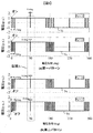
- Shown in FIG. 11 shows a pulse pattern of the present invention corrected based on this pulse pattern.
- Each parameter of the corrected pulse pattern shown in FIG. 11 is as follows.
- FIG. 12 shows a pulse pattern when the modulation rate Kh * of the pulse pattern shown in FIG. 11 is changed to 1.15-1.21. These pulse patterns have the following characteristics.
- Fig. 13 shows the pulse pattern when the modulation factor Kh * is greater than 1.22.
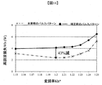
- the harmonic loss of the harmonic order n greater than 200 is zero.
- the pulse pattern of the present invention can reduce the harmonic loss Wh compared with the pulse pattern before correction, and the reduction amount is 43% at the maximum.
- FIG. 15 is a block diagram of the second embodiment, and FIG. 21 shows its elements. However, the same points as in Example 1 are omitted.
- the carrier wave generator 3 outputs a carrier wave Vc * based on the carrier frequency fc *.
- the asynchronous correction phase calculator 16 calculates the second zero hold phase ⁇ 02, the second zero cross phase ⁇ 12, and the second peak phase ⁇ 22 based on the base number B and the pulse number Pn.
- the correction signal generator 13 generates an asynchronous correction signal A2 based on the second zero hold phase ⁇ 02, the second zero cross phase ⁇ 12, the second peak phase ⁇ 22, the zero cross correction amount A1, the peak correction amount Am, and the voltage phase ⁇ *. To do.
- Example 2 harmonic loss in the overmodulation region in asynchronous PWM control is reduced.
- the carrier frequency fc * is fixed regardless of the fundamental frequency f1 *. For this reason, the zero cross points at which the signs of the carrier wave Vc * and the signal wave Vu * are switched do not match as shown in B of FIG.
- the pulse voltage Vu has an aperiodic waveform with respect to the signal cycle T1 because the zero-cross points of the signal wave Vu * and the carrier wave Vc * do not match.
- the waveform is a periodic waveform with respect to the period T1 which is the least common multiple of the period T1 of the signal wave and the period Tc of the carrier wave. Therefore, in the second embodiment, the harmonic voltage Vn is obtained as (Equation 18) based on the least common period T.
- harmonic components are also generated in the lower region than the fundamental component.
- the control angle ⁇ is calculated so as to reduce or minimize (Equation 19) obtained by substituting (Equation 18) into (Equation 6).
- the modulation factor Kh * which is the constraint condition of Equation (19), is calculated with being fixed at 1.2.
- Fig. 18 shows the effect of Example 2.
- the harmonic loss Wh can be reduced in the conventional method and the present invention even though the effective value of the voltage harmonic Vn is equal.
- the harmonic loss Wh can be reduced despite the increase in the effective value of the voltage harmonic Vn.
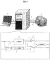
- FIG. 19 is a configuration diagram of the third embodiment, and shows a drive system that mounts the first or second embodiment and drives the AC motor 1.
- Example 3 a torque command ⁇ * or a frequency command f * is output from a host device such as the computer 17.
- the V / f control unit 18 and the vector control unit 19 calculate the fundamental frequency f1 * and the modulation factor Kh * based on the torque command ⁇ * or the frequency command f *.
- the control mode conversion unit 20 switches between the torque command ⁇ * and the frequency command f *.
- the control selection unit 21 switches between the V / f control unit 18 and the vector control unit 19.
- the phase calculation unit 22 calculates the voltage phase ⁇ * based on the fundamental frequency f1 *.
- the fundamental frequency f1 *, voltage phase ⁇ *, and modulation factor Kh * calculated in the third embodiment are output to the motor control device of the first or second embodiment, and the AC motor 1 is driven.
- the command value can be arbitrarily set in the torque command ⁇ * or the frequency command f * and the vector control unit 19 or the V / f control unit 18.
- Phase calculation unit VDC DC voltage Vu , Vv, Vw... U phase pulse voltage, V phase pulse voltage, W phase pulse voltage Iu, Iv, Iw... U phase current, V phase current, W phase current Vu *, Vv *, Vw *... U phase signal wave, V phase signal wave, W phase signal wave Vu2 *, Vv2 *, Vw2 * ... U phase correction signal wave, V phase correction signal wave, W phase correction signal wave Vuv ... Line voltage Vc * ... Carrier wave P ... Pattern A ... Synchronization correction signal, A * ... Final correction signal A1 ... Zero cross correction amount Am ... Peak correction amount Vn ... Harmonic voltage Guu, Gup ... U phase gate signal Gvu, Gvp ...
Landscapes
- Engineering & Computer Science (AREA)
- Power Engineering (AREA)
- Control Of Ac Motors In General (AREA)
- Inverter Devices (AREA)
Abstract
Le problème abordé par la présente invention est de réduire ou de réduire au minimum les pertes harmoniques qui surviennent lorsqu'un moteur à courant alternatif est attaqué dans une région de surmodulation. Une onde de signal de correction finale est modifiée de zéro à un signal de correction synchrone lorsqu'un taux de modulation a atteint une valeur prédéterminée supérieure ou égale à un, et une amplitude finale est modifiée d'une première amplitude à une amplitude fixe lorsque le taux de modulation a atteint la valeur prédéterminée supérieure ou égale à un.
Priority Applications (2)
| Application Number | Priority Date | Filing Date | Title |
|---|---|---|---|
| CN201780007490.XA CN108476011B (zh) | 2016-03-15 | 2017-01-30 | 电动机的控制装置和驱动系统 |
| EP17766080.0A EP3432467B1 (fr) | 2016-03-15 | 2017-01-30 | Dispositif de commande de moteur et système d'entraînement |
Applications Claiming Priority (2)
| Application Number | Priority Date | Filing Date | Title |
|---|---|---|---|
| JP2016-050388 | 2016-03-15 | ||
| JP2016050388A JP6674804B2 (ja) | 2016-03-15 | 2016-03-15 | モータの制御装置および駆動システム |
Publications (1)
| Publication Number | Publication Date |
|---|---|
| WO2017159072A1 true WO2017159072A1 (fr) | 2017-09-21 |
Family
ID=59852256
Family Applications (1)
| Application Number | Title | Priority Date | Filing Date |
|---|---|---|---|
| PCT/JP2017/003085 WO2017159072A1 (fr) | 2016-03-15 | 2017-01-30 | Dispositif de commande de moteur et système d'entraînement |
Country Status (4)
| Country | Link |
|---|---|
| EP (1) | EP3432467B1 (fr) |
| JP (1) | JP6674804B2 (fr) |
| CN (1) | CN108476011B (fr) |
| WO (1) | WO2017159072A1 (fr) |
Cited By (1)
| Publication number | Priority date | Publication date | Assignee | Title |
|---|---|---|---|---|
| CN111342726A (zh) * | 2020-03-26 | 2020-06-26 | 武汉科技大学 | 一种永磁同步电机直接转矩控制方法及系统 |
Families Citing this family (2)
| Publication number | Priority date | Publication date | Assignee | Title |
|---|---|---|---|---|
| CN111585499B (zh) * | 2019-02-18 | 2023-07-21 | 本田技研工业株式会社 | 控制装置、车辆系统及控制方法 |
| JP6989574B2 (ja) | 2019-09-25 | 2022-01-05 | 本田技研工業株式会社 | 制御装置、車両システム及び制御方法 |
Citations (5)
| Publication number | Priority date | Publication date | Assignee | Title |
|---|---|---|---|---|
| JP2007143316A (ja) * | 2005-11-18 | 2007-06-07 | Mitsubishi Electric Corp | モータ制御装置 |
| JP2013141336A (ja) * | 2011-12-28 | 2013-07-18 | Hitachi Appliances Inc | モータ制御装置および空気調和機 |
| JP2014072936A (ja) * | 2012-09-28 | 2014-04-21 | Hitachi Ltd | 交流電動機駆動システム及び電動機車両 |
| JP2015053824A (ja) | 2013-09-09 | 2015-03-19 | 株式会社日立製作所 | モータ駆動システムおよび該システムを搭載する電気鉄道車両 |
| JP2016005378A (ja) * | 2014-06-18 | 2016-01-12 | 株式会社日立製作所 | インバータおよびこれを用いた駆動システム |
Family Cites Families (2)
| Publication number | Priority date | Publication date | Assignee | Title |
|---|---|---|---|---|
| JP4858597B2 (ja) * | 2008-11-28 | 2012-01-18 | 株式会社デンソー | 回転機の制御装置及びその製造方法 |
| JP4911241B1 (ja) * | 2010-11-16 | 2012-04-04 | ダイキン工業株式会社 | 電力変換装置 |
-
2016
- 2016-03-15 JP JP2016050388A patent/JP6674804B2/ja active Active
-
2017
- 2017-01-30 CN CN201780007490.XA patent/CN108476011B/zh not_active Expired - Fee Related
- 2017-01-30 EP EP17766080.0A patent/EP3432467B1/fr active Active
- 2017-01-30 WO PCT/JP2017/003085 patent/WO2017159072A1/fr active Application Filing
Patent Citations (5)
| Publication number | Priority date | Publication date | Assignee | Title |
|---|---|---|---|---|
| JP2007143316A (ja) * | 2005-11-18 | 2007-06-07 | Mitsubishi Electric Corp | モータ制御装置 |
| JP2013141336A (ja) * | 2011-12-28 | 2013-07-18 | Hitachi Appliances Inc | モータ制御装置および空気調和機 |
| JP2014072936A (ja) * | 2012-09-28 | 2014-04-21 | Hitachi Ltd | 交流電動機駆動システム及び電動機車両 |
| JP2015053824A (ja) | 2013-09-09 | 2015-03-19 | 株式会社日立製作所 | モータ駆動システムおよび該システムを搭載する電気鉄道車両 |
| JP2016005378A (ja) * | 2014-06-18 | 2016-01-12 | 株式会社日立製作所 | インバータおよびこれを用いた駆動システム |
Non-Patent Citations (1)
| Title |
|---|
| See also references of EP3432467A4 |
Cited By (2)
| Publication number | Priority date | Publication date | Assignee | Title |
|---|---|---|---|---|
| CN111342726A (zh) * | 2020-03-26 | 2020-06-26 | 武汉科技大学 | 一种永磁同步电机直接转矩控制方法及系统 |
| CN111342726B (zh) * | 2020-03-26 | 2023-05-30 | 武汉科技大学 | 一种永磁同步电机直接转矩控制方法及系统 |
Also Published As
| Publication number | Publication date |
|---|---|
| EP3432467B1 (fr) | 2022-04-06 |
| JP2017169295A (ja) | 2017-09-21 |
| EP3432467A4 (fr) | 2019-10-23 |
| JP6674804B2 (ja) | 2020-04-01 |
| CN108476011A (zh) | 2018-08-31 |
| CN108476011B (zh) | 2021-05-28 |
| EP3432467A1 (fr) | 2019-01-23 |
Similar Documents
| Publication | Publication Date | Title |
|---|---|---|
| JP5866065B2 (ja) | 交流電動機の制御装置 | |
| JP6566105B2 (ja) | 電力変換装置 | |
| WO2014196013A1 (fr) | Dispositif de conversion d'énergie | |
| Videt et al. | PWM strategy for the cancellation of common-mode voltage generated by three-phase back-to-back inverters | |
| EP3528383A1 (fr) | Dispositif de commande et procédé de commande pour moteur à courant alternatif, et système d'entraînement de moteur à courant alternatif | |
| WO2015115223A1 (fr) | Procédé de commande d'onduleur et onduleur du type à tension | |
| JP6239448B2 (ja) | インバータおよびこれを用いた駆動システム | |
| WO2017119214A1 (fr) | Dispositif de conversion d'énergie électrique | |
| WO2017159072A1 (fr) | Dispositif de commande de moteur et système d'entraînement | |
| WO2016152250A1 (fr) | Dispositif de commande de moteur | |
| Mink et al. | Feedback control of high-speed PMSM with synchronous optimal PWM | |
| JP2017093077A (ja) | オープン巻線システムの制御装置および制御方法 | |
| JP2008048530A (ja) | 交流−交流直接変換装置の空間ベクトル変調方法 | |
| JP4893152B2 (ja) | 交流−交流直接変換装置の空間ベクトル変調方法 | |
| JP2007116856A (ja) | 電力変換装置 | |
| WO2015125540A1 (fr) | Procédé de commande d'onduleur et onduleur | |
| Corzine et al. | Distributed control of hybrid motor drives | |
| JP5761095B2 (ja) | 回転機の制御装置 | |
| Holagh et al. | Improved selective harmonic elimination for reducing torque harmonics of induction motors in wide DC bus voltage variations | |
| JP2006280063A (ja) | 交流交流直接電力変換器の制御装置 | |
| Mirazimi et al. | Space vector PWM method for two-phase three-leg inverters | |
| Nishizawa et al. | Reduction of dc-link current harmonics over wide power-factor range for three-phase VSI using single-carrier-comparison continuous PWM | |
| JP4905174B2 (ja) | 交流交流直接変換器の制御装置 | |
| JP2006141175A (ja) | 交流交流直接変換器の電動機制御装置 | |
| JP2014039425A (ja) | インバータのpwm電圧発生装置 |
Legal Events
| Date | Code | Title | Description |
|---|---|---|---|
| NENP | Non-entry into the national phase |
Ref country code: DE |
|
| 121 | Ep: the epo has been informed by wipo that ep was designated in this application |
Ref document number: 17766080 Country of ref document: EP Kind code of ref document: A1 |
|
| WWE | Wipo information: entry into national phase |
Ref document number: 2017766080 Country of ref document: EP |
|
| ENP | Entry into the national phase |
Ref document number: 2017766080 Country of ref document: EP Effective date: 20181015 |