WO2017159072A1 - Motor control device and drive system - Google Patents
Motor control device and drive system Download PDFInfo
- Publication number
- WO2017159072A1 WO2017159072A1 PCT/JP2017/003085 JP2017003085W WO2017159072A1 WO 2017159072 A1 WO2017159072 A1 WO 2017159072A1 JP 2017003085 W JP2017003085 W JP 2017003085W WO 2017159072 A1 WO2017159072 A1 WO 2017159072A1
- Authority
- WO
- WIPO (PCT)
- Prior art keywords
- phase
- voltage
- correction
- control device
- motor control
- Prior art date
Links
Images


Classifications
-
- H—ELECTRICITY
- H02—GENERATION; CONVERSION OR DISTRIBUTION OF ELECTRIC POWER
- H02P—CONTROL OR REGULATION OF ELECTRIC MOTORS, ELECTRIC GENERATORS OR DYNAMO-ELECTRIC CONVERTERS; CONTROLLING TRANSFORMERS, REACTORS OR CHOKE COILS
- H02P27/00—Arrangements or methods for the control of AC motors characterised by the kind of supply voltage
- H02P27/04—Arrangements or methods for the control of AC motors characterised by the kind of supply voltage using variable-frequency supply voltage, e.g. inverter or converter supply voltage
- H02P27/06—Arrangements or methods for the control of AC motors characterised by the kind of supply voltage using variable-frequency supply voltage, e.g. inverter or converter supply voltage using dc to ac converters or inverters
- H02P27/08—Arrangements or methods for the control of AC motors characterised by the kind of supply voltage using variable-frequency supply voltage, e.g. inverter or converter supply voltage using dc to ac converters or inverters with pulse width modulation
-
- H—ELECTRICITY
- H02—GENERATION; CONVERSION OR DISTRIBUTION OF ELECTRIC POWER
- H02P—CONTROL OR REGULATION OF ELECTRIC MOTORS, ELECTRIC GENERATORS OR DYNAMO-ELECTRIC CONVERTERS; CONTROLLING TRANSFORMERS, REACTORS OR CHOKE COILS
- H02P21/00—Arrangements or methods for the control of electric machines by vector control, e.g. by control of field orientation
-
- H—ELECTRICITY
- H02—GENERATION; CONVERSION OR DISTRIBUTION OF ELECTRIC POWER
- H02P—CONTROL OR REGULATION OF ELECTRIC MOTORS, ELECTRIC GENERATORS OR DYNAMO-ELECTRIC CONVERTERS; CONTROLLING TRANSFORMERS, REACTORS OR CHOKE COILS
- H02P27/00—Arrangements or methods for the control of AC motors characterised by the kind of supply voltage
- H02P27/04—Arrangements or methods for the control of AC motors characterised by the kind of supply voltage using variable-frequency supply voltage, e.g. inverter or converter supply voltage
-
- H—ELECTRICITY
- H02—GENERATION; CONVERSION OR DISTRIBUTION OF ELECTRIC POWER
- H02P—CONTROL OR REGULATION OF ELECTRIC MOTORS, ELECTRIC GENERATORS OR DYNAMO-ELECTRIC CONVERTERS; CONTROLLING TRANSFORMERS, REACTORS OR CHOKE COILS
- H02P2209/00—Indexing scheme relating to controlling arrangements characterised by the waveform of the supplied voltage or current
- H02P2209/09—PWM with fixed limited number of pulses per period
Definitions
- the present invention relates to a motor control device and a drive system for reducing harmonic loss.
- the loss is divided into a loss generated in the motor (hereinafter referred to as motor loss) and a loss generated in the inverter (hereinafter referred to as inverter loss).
- the motor loss includes a loss due to the fundamental component (hereinafter referred to as fundamental loss) and a loss due to the harmonic component (hereinafter referred to as harmonic loss).
- the inverter loss includes a loss caused by the on / off operation of the switching element (hereinafter referred to as switching loss) and a loss generated when the switching element is conducted (hereinafter referred to as conduction loss).
- ⁇ Fundamental loss is reduced by adopting variable speed drive by inverter compared to constant speed drive by commercial power supply.
- the voltage and current are distorted by the switching operation, and harmonic components are generated, so that harmonic loss increases.
- Harmonic components and harmonic losses can be reduced by improving the carrier frequency of the inverter.
- switching loss increases at the same time, it is desirable to reduce harmonic loss without increasing the carrier frequency.
- harmonic components and harmonic loss are remarkably increased, and reduction thereof is desired.
- Patent Document 1 is a technology for synchronous PWM control for railways.
- the pulse voltage is near the zero cross point (0,180 deg) and peak point (90,270 deg) of the fundamental phase. It is turned on or off once or more, and is kept on or off in other phase regions.
- Patent Document 1 The problem of Patent Document 1 is the method for synchronous PWM control, so it does not support asynchronous PWM control, and because it is for railways, the upper limit of the carrier frequency is low, and it is only in a narrow drive range. The effect does not appear.
- an object of the present invention is to reduce or minimize harmonic loss generated when an AC motor is driven in an overmodulation region.
- the present invention switches the final correction signal wave from 0 to the synchronization correction signal when the modulation rate reaches a predetermined value of 1 or more, and the modulation rate is 1 or more.
- the predetermined value is reached, the final amplitude is switched from the first amplitude to the fixed amplitude.
- harmonic loss generated when an AC motor is driven in an overmodulation region using an inverter can be reduced.
- effects such as higher output of the AC motor or downsizing of the cooling system can be obtained.
- Example 1 will be described with reference to FIGS. 1 to 14 and FIG.
- Fig. 1 is a block diagram of the motor control device in the first embodiment, and Fig. 2 shows its elements.
- the inverter 2 can control the AC motor 1 by converting the DC voltage VDC into an arbitrary frequency.
- AC motor 1 is applied with a three-phase AC current (U-phase current Iu, V-phase current Iv, W-phase) by applying a pulse voltage (U-phase pulse voltage Vu, V-phase pulse voltage Vv, W-phase pulse voltage Vw).
- the current Iw flows and is driven at the drive frequency f.
- line voltage Vuv the voltage applied between the U-V phases of AC motor 1 is referred to as line voltage Vuv.
- the frequency calculation unit 3 calculates the carrier frequency fc * and the base number B based on the fundamental frequency f1 *.
- the base number B is the ratio of the carrier frequency fc * and the fundamental frequency f1 *.
- the frequency correction unit 4 calculates the correction carrier frequency fc2 * based on the base number B and the pattern P.
- the first modulation mode determination unit 5 switches the final carrier frequency fc2 ** from the carrier frequency fc * to the corrected carrier frequency fc2 * when the modulation factor Kh * reaches a predetermined value of 1 or more.
- the carrier wave generator 6 outputs a carrier wave Vc * based on the final carrier frequency fc **.
- the carrier wave Vc * is a triangular wave having an amplitude of 1 (normalized by the DC voltage VDC / 2) as shown in FIG. 3, and is a function depending on the voltage phase ⁇ *.
- the amplitude calculator 7 calculates the first amplitude Amp1 based on the modulation factor Kh *.
- the second modulation mode determination unit 8 switches the final amplitude Amp from the first amplitude Amp1 to the fixed amplitude Amp2 when the modulation factor Kh * reaches a predetermined value of 1 or more.
- the signal wave generator 9 outputs a signal wave (U phase signal wave Vu *, V phase signal wave Vv *, W phase signal wave Vw *) based on the voltage phase ⁇ * and the final amplitude Amp.
- the signal wave Vu * is a sine wave as shown in FIG. 3, and is a function depending on the voltage phase ⁇ *.
- the correction amount calculation unit 10 calculates the pulse number Pn, the zero cross correction amount A1, and the peak correction amount Am based on the modulation factor Kh *, the voltage phase ⁇ *, and the base number B.
- the pattern determination unit 11 determines the pattern P based on the number of bases. Here, when the pattern P is 1, it is the first pattern, and when P is 2, it is the second pattern.
- the synchronization correction phase calculation unit 12 calculates the zero hold phase ⁇ 0, the zero cross phase ⁇ 1, and the peak phase ⁇ 2 based on the number of pulses Pn, the pattern P, the correction carrier frequency fc2 *, and the fundamental frequency f1 *.
- the zero holding phase ⁇ 0 is a phase corresponding to a quarter period of the carrier wave Vc *.
- the correction signal generator 13 generates the synchronization correction signal A based on the zero hold phase ⁇ 0, the zero cross phase ⁇ 1, the peak phase ⁇ 2, the zero cross correction amount A1, the peak correction amount Am, and the voltage phase ⁇ *.
- the synchronization correction signal A is a function that depends on the voltage phase ⁇ *.
- the third modulation mode determination unit 14 switches the final correction signal A * from 0 to the synchronization correction signal A when the modulation factor Kh * reaches a predetermined value of 1 or more.
- the PWM controller 15 compares the correction signal waves Vu2 *, Vv2 *, Vw2 * and the carrier wave Vc * obtained by adding the final correction signal A * to the signal waves Vu *, Vv *, Vw *,
- the gate signals Gun, Gup, Gvn, Gvp, Gwn, Gwv are generated and output to the inverter 2.
- the inverter 2 turns on or off the switching element based on the gate signals Gun, Gup, Gvn, Gvp, Gwn, Gwv, and applies the pulse voltages Vu, Vv, Vw to the AC motor 1.
- FIG. 2 is a block diagram element of the correction amount calculation unit 10.
- the control angle calculation unit 10a calculates the control angle ⁇ and the pulse number Pn based on the modulation rate Kh * and the base number B.
- the peak correction amount calculation unit 10b calculates the peak correction amount Am based on the modulation rate.
- the zero cross correction amount calculation unit 10c calculates the zero cross correction amount A1 based on the number of pulses Pn and the modulation rate Kh *.
- the PWM control unit 15 acquires the values of the signal waves Vu *, Vv *, Vw * every half cycle of the carrier wave Vc *, and compares them with the carrier wave Vc * to obtain the gate signals Gun, Gup, Gvn, Gvp. , Gwn, Gwv high or low.
- the inverter 2 outputs pulse voltages Vu, Vv, Vw to the AC motor 1 in accordance with the high or low of the gate signals Gun, Gup, Gvn, Gvp, Gwn, Gwv.
- the gate signal Gup is high, Gun is low, and the pulse voltage Vu is turned on.
- PWM control includes synchronous PWM control and asynchronous PWM control.
- Example 1 describes synchronous PWM control.
- the carrier frequency fc * is calculated by the frequency calculation unit 3 to be an integral multiple of the fundamental frequency f1 *, and the pulse voltage Vu is calculated with respect to the period T1 of the signal waves Vu *, Vv *, and Vw *.
- the carrier frequency fc * is calculated so as to satisfy (Equation 1) in order to keep the pulse voltages Vu, Vv, and Vw symmetrical.
- Pn is the number of pulses of the pulse voltages Vu, Vv, Vw per fundamental wave cycle.
- the pulse number Pn of the pulse pattern shown in FIG. 3 (a) is 9 pulses.
- F cmax is the maximum carrier frequency at which synchronous PWM control is possible.
- the maximum carrier frequency fc of a railway inverter is about several hundred Hz
- the maximum carrier frequency fcmax of a general-purpose inverter is about several kHz.
- Asynchronous PWM control is used when PWM control is performed at a carrier frequency fc * higher than the maximum carrier frequency fcmax. The above is the operating principle of PWM control.
- the harmonic loss Wh which is a problem with PWM control, will be described.
- PWM control distortion occurs in the voltage and current as the switching element of the inverter 2 is turned on or off. This distortion can be expressed as a harmonic component shown in FIG. 2 (b), which generates a harmonic loss Wh.
- the overmodulation region is a region where the modulation factor Kh * exceeds 1 (p.u.), and a region where the modulation factor Kh * is less than 1 (p.u.) is called a modulation region.
- the number of pulses Pn (7 pulses) in the overmodulation region is smaller than the number of pulses Pn (9 pulses) in the modulation region.
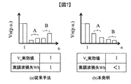
- the effective value of the harmonic voltage Vn increases and the harmonic loss Wh also increases. For example, as shown in Fig.
- the effective value of the 13th harmonic voltage Vn is 0.008 p.u. when the motor is driven in the modulation range.
- the effective value is 0.291 p.u, which is approximately 30 times that of the motor driven in the modulation range.
- the harmonic voltage Vn is an effective value of the harmonic component determined by the pulse pattern, and a phase ⁇ (hereinafter referred to as a control angle ⁇ ) in which the pulse voltage Vu, Vv, Vw switches from on to off or from off to on. ) And is expressed as (Equation 2).
- the modulation factor Kh * depends on the control angle ⁇ and is expressed as (Equation 3).
- FIG. 5 shows the waveform diagram of the third harmonic superposition method.
- the first amplitude Amp1 of the signal waves Vu *, Vv *, Vw * in the third-order harmonic superposition method is calculated as (Equation 4) based on the modulation rate Kh *.
- the modulation factor Kh * 1.15
- the difference from the amplitude of the carrier wave Vc * is 0.15 pu. It becomes. Therefore, in the third harmonic superposition method, the effective value of the harmonic voltage Vn in the overmodulation region is reduced compared to the sine wave method.
- the harmonic loss Wh is the sum of the eddy current generated in the magnet of the AC motor 1 and the hysteresis loss generated in the electromagnetic steel sheet, and is proportional to the square of the harmonic current In.
- the harmonic current In can be expressed as (Equation 5) using the harmonic voltage Vn of (Equation 2).
- the loss coefficient ⁇ is a coefficient representing the characteristic of the harmonic loss Wh of the AC motor 1, and is determined as follows depending on the factor (FIG. 20) of the harmonic loss Wh of the AC motor 1.
- the loss factor ⁇ is between 0 and 2.
- the loss coefficient ⁇ is 0 ⁇ ⁇ ⁇ 1.
- the harmonic loss Wh does not have frequency dependence, so the harmonic current In and the harmonic loss Wh are in a proportional relationship. Therefore, by reducing the harmonic voltage Vn, the harmonic current In is also reduced, and as a result, the harmonic loss Wh is reduced.
- the harmonic loss Wh is frequency-dependent, the loss coefficient ⁇ is larger than 0, and therefore the harmonic resistance n ⁇ and the harmonic order n have the relationship shown in FIG. That is, the higher the harmonic order n, the higher the harmonic resistance n ⁇ . Therefore, the higher harmonic voltage Vn than the lower harmonic voltage Vn affects the harmonic loss Wh. Therefore, the harmonic loss Wh is greatly reduced by reducing the higher-order harmonic voltage Vn shown in B of FIG. 7 even if the increase of the lower-order harmonic voltage Vn shown in A of FIG. 7 is allowed. can do. That is, it is necessary to reduce the effective value of the higher-order harmonic voltage Vn in accordance with the loss factor ⁇ .
- Equation 7 In order to determine the pulse pattern in consideration of the frequency dependence of the harmonic loss Wh, (Equation 7) is used as the optimization objective function, and the control angle ⁇ is calculated so as to reduce or minimize this.
- the modulation factor Kh * is influenced by the control angle ⁇ , and is therefore a constraint condition for optimization.
- the modulation factor Kh * which is a constraint condition, is fixed at 1.2.
- There is a pattern that turns off at the phase ⁇ * 0 deg.
- the former is referred to as a first pattern, and the latter is referred to as a second pattern.
- the frequency correction unit 4, the correction amount calculation unit 10, the synchronization correction phase calculation unit 12, and the correction signal generation unit 13 are used to generate the synchronization correction signal A, and the above features (a) to (d)
- the pulse pattern that holds the constraints (A) and (B) is output to the inverter 2. The principle will be described below.
- the frequency correction unit 4 calculates a correction signal fc2 * that satisfies the constraints of (Equation 8) or (Equation 9) and (Equation 10), (Equation 1) based on the base number B and the pattern P.
- the pulse voltage Vu holds (b)-(d) while satisfying the constraints (A) and (B).
- the zero retention phase ⁇ 0 is calculated based on (Equation 11).
- the correction base number B2 is a ratio of the correction carrier frequency fc2 * and the fundamental frequency f1 *.
- the zero cross phase ⁇ 1 is calculated based on (Equation 12) or (Equation 13).
- the peak correction amount A1 is calculated as (Equation 15) based on the modulation factor Kh *.
- the peak amount correction amount A1 is calculated as (Equation 16) based on the control angle ⁇ without depending on the modulation factor Kh *.
- the control angle ⁇ is a value optimized to reduce or minimize the harmonic loss Wh based on (Equation 7).
- the synchronization correction signal A is generated to satisfy (Equation 17).
- the synchronization correction signal A when the voltage phase ⁇ * is 90-360 (deg) is determined by the symmetry of the waveform.
- Shown in FIG. 11 shows a pulse pattern of the present invention corrected based on this pulse pattern.
- Each parameter of the corrected pulse pattern shown in FIG. 11 is as follows.
- FIG. 12 shows a pulse pattern when the modulation rate Kh * of the pulse pattern shown in FIG. 11 is changed to 1.15-1.21. These pulse patterns have the following characteristics.
- Fig. 13 shows the pulse pattern when the modulation factor Kh * is greater than 1.22.
- the harmonic loss of the harmonic order n greater than 200 is zero.
- the pulse pattern of the present invention can reduce the harmonic loss Wh compared with the pulse pattern before correction, and the reduction amount is 43% at the maximum.
- FIG. 15 is a block diagram of the second embodiment, and FIG. 21 shows its elements. However, the same points as in Example 1 are omitted.
- the carrier wave generator 3 outputs a carrier wave Vc * based on the carrier frequency fc *.
- the asynchronous correction phase calculator 16 calculates the second zero hold phase ⁇ 02, the second zero cross phase ⁇ 12, and the second peak phase ⁇ 22 based on the base number B and the pulse number Pn.
- the correction signal generator 13 generates an asynchronous correction signal A2 based on the second zero hold phase ⁇ 02, the second zero cross phase ⁇ 12, the second peak phase ⁇ 22, the zero cross correction amount A1, the peak correction amount Am, and the voltage phase ⁇ *. To do.
- Example 2 harmonic loss in the overmodulation region in asynchronous PWM control is reduced.
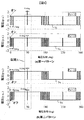
- the carrier frequency fc * is fixed regardless of the fundamental frequency f1 *. For this reason, the zero cross points at which the signs of the carrier wave Vc * and the signal wave Vu * are switched do not match as shown in B of FIG.
- the pulse voltage Vu has an aperiodic waveform with respect to the signal cycle T1 because the zero-cross points of the signal wave Vu * and the carrier wave Vc * do not match.
- the waveform is a periodic waveform with respect to the period T1 which is the least common multiple of the period T1 of the signal wave and the period Tc of the carrier wave. Therefore, in the second embodiment, the harmonic voltage Vn is obtained as (Equation 18) based on the least common period T.
- harmonic components are also generated in the lower region than the fundamental component.
- the control angle ⁇ is calculated so as to reduce or minimize (Equation 19) obtained by substituting (Equation 18) into (Equation 6).
- the modulation factor Kh * which is the constraint condition of Equation (19), is calculated with being fixed at 1.2.
- Fig. 18 shows the effect of Example 2.
- the harmonic loss Wh can be reduced in the conventional method and the present invention even though the effective value of the voltage harmonic Vn is equal.
- the harmonic loss Wh can be reduced despite the increase in the effective value of the voltage harmonic Vn.
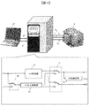
- FIG. 19 is a configuration diagram of the third embodiment, and shows a drive system that mounts the first or second embodiment and drives the AC motor 1.
- Example 3 a torque command ⁇ * or a frequency command f * is output from a host device such as the computer 17.
- the V / f control unit 18 and the vector control unit 19 calculate the fundamental frequency f1 * and the modulation factor Kh * based on the torque command ⁇ * or the frequency command f *.
- the control mode conversion unit 20 switches between the torque command ⁇ * and the frequency command f *.
- the control selection unit 21 switches between the V / f control unit 18 and the vector control unit 19.
- the phase calculation unit 22 calculates the voltage phase ⁇ * based on the fundamental frequency f1 *.
- the fundamental frequency f1 *, voltage phase ⁇ *, and modulation factor Kh * calculated in the third embodiment are output to the motor control device of the first or second embodiment, and the AC motor 1 is driven.
- the command value can be arbitrarily set in the torque command ⁇ * or the frequency command f * and the vector control unit 19 or the V / f control unit 18.
- Phase calculation unit VDC DC voltage Vu , Vv, Vw... U phase pulse voltage, V phase pulse voltage, W phase pulse voltage Iu, Iv, Iw... U phase current, V phase current, W phase current Vu *, Vv *, Vw *... U phase signal wave, V phase signal wave, W phase signal wave Vu2 *, Vv2 *, Vw2 * ... U phase correction signal wave, V phase correction signal wave, W phase correction signal wave Vuv ... Line voltage Vc * ... Carrier wave P ... Pattern A ... Synchronization correction signal, A * ... Final correction signal A1 ... Zero cross correction amount Am ... Peak correction amount Vn ... Harmonic voltage Guu, Gup ... U phase gate signal Gvu, Gvp ...
Abstract
The present invention addresses the problem of reducing or minimizing a harmonic loss that occurs when an alternating-current motor is driven in an over-modulation region. The final correction signal wave is changed from zero to a synchronous correction signal when a modulation rate has reached a predetermined value equal to or greater than one, and the final amplitude is changed from a first amplitude to a fixed amplitude when the modulation rate has reached the predetermined value equal to or greater than one.
Description
本発明は,高調波損失を低減するためモータ制御装置および駆動システムに関する。
The present invention relates to a motor control device and a drive system for reducing harmonic loss.
インバータを用いたPWM制御によるモータ駆動システムにおいて,各種損失の低減が望まれている。損失は,モータに発生する損失(以下,モータ損失)と,インバータで発生する損失(以下,インバータ損失)に分けられる。モータ損失は,基本波成分に起因した損失(以下,基本波損失)と,高調波成分に起因した損失(以下,高調波損失)がある。インバータ損失は,スイッチング素子のオンオフ動作に起因する損失(以下,スイッチング損失)と,スイッチング素子の導通時に発生する損失(以下,導通損失)がある。
In the motor drive system by PWM control using an inverter, reduction of various losses is desired. The loss is divided into a loss generated in the motor (hereinafter referred to as motor loss) and a loss generated in the inverter (hereinafter referred to as inverter loss). The motor loss includes a loss due to the fundamental component (hereinafter referred to as fundamental loss) and a loss due to the harmonic component (hereinafter referred to as harmonic loss). The inverter loss includes a loss caused by the on / off operation of the switching element (hereinafter referred to as switching loss) and a loss generated when the switching element is conducted (hereinafter referred to as conduction loss).
基本波損失は,インバータによる可変速駆動を採用することによって,商用電源による一定速駆動に比べて低減される。しかし,スイッチング動作により電圧・電流が歪み,高調波成分が発生するため,高調波損失が増加する。高調波成分および高調波損失は,インバータのキャリア周波数の向上により低減できる。しかし,同時にスイッチング損失が増加するため,キャリア周波数を増加せずに高調波損失を低減することが望まれる。特に,過変調域でモータを駆動すると,高調波成分および高調波損失が顕著に増加することが知られており,その低減が望まれている。
基本 Fundamental loss is reduced by adopting variable speed drive by inverter compared to constant speed drive by commercial power supply. However, the voltage and current are distorted by the switching operation, and harmonic components are generated, so that harmonic loss increases. Harmonic components and harmonic losses can be reduced by improving the carrier frequency of the inverter. However, since switching loss increases at the same time, it is desirable to reduce harmonic loss without increasing the carrier frequency. In particular, it is known that when a motor is driven in an overmodulation region, harmonic components and harmonic loss are remarkably increased, and reduction thereof is desired.
特許文献1は,鉄道向け同期PWM制御の技術であり,過変調域で発生する高調波損失低減のため,基本波位相のゼロクロス点(0,180deg)およびピーク点(90,270deg)近傍でパルス電圧が1回以上オンまたはオフ動作させ,その他の位相領域ではオンまたはオフ状態を保持させている。
Patent Document 1 is a technology for synchronous PWM control for railways. In order to reduce the harmonic loss that occurs in the overmodulation region, the pulse voltage is near the zero cross point (0,180 deg) and peak point (90,270 deg) of the fundamental phase. It is turned on or off once or more, and is kept on or off in other phase regions.
特許文献1の問題点は,同期PWM制御向けの手法であるため,非同期PWM制御には対応していないことと,鉄道向けであるため,キャリア周波数の上限が低く,狭い範囲の駆動領域でしか効果が表れないことである。
The problem of Patent Document 1 is the method for synchronous PWM control, so it does not support asynchronous PWM control, and because it is for railways, the upper limit of the carrier frequency is low, and it is only in a narrow drive range. The effect does not appear.
過変調域の高調波損失を低減し,その効果が表れる駆動範囲を広げるためには,非同期PWM制御の対応,および,キャリア周波数の上限を高周波化させる必要がある。
In order to reduce the harmonic loss in the overmodulation range and expand the drive range where the effect appears, it is necessary to support asynchronous PWM control and increase the upper limit of the carrier frequency.
そこで、本発明の課題は,交流モータを過変調域で駆動した際に生じる高調波損失を低減あるいは最小化することである。
Therefore, an object of the present invention is to reduce or minimize harmonic loss generated when an AC motor is driven in an overmodulation region.
上記課題を解決するために、本発明は、一例として、変調率が1以上の所定の値に達した場合,最終補正信号波を0から前記同期補正信号に切り換え、前記変調率が1以上の所定の値に達した場合,最終振幅を前記第一振幅から固定振幅に切り換える。
In order to solve the above problem, as an example, the present invention switches the final correction signal wave from 0 to the synchronization correction signal when the modulation rate reaches a predetermined value of 1 or more, and the modulation rate is 1 or more. When the predetermined value is reached, the final amplitude is switched from the first amplitude to the fixed amplitude.
本発明により,インバータを用いて交流モータを過変調域で駆動した際に発生する高調波損失を低減することができる。これにより,交流モータの高出力化あるいは冷却系の小型化などの効果を得ることができる。
According to the present invention, harmonic loss generated when an AC motor is driven in an overmodulation region using an inverter can be reduced. As a result, effects such as higher output of the AC motor or downsizing of the cooling system can be obtained.
図1~図14および図20を用いて実施例1を説明する。
Example 1 will be described with reference to FIGS. 1 to 14 and FIG.
図1は,実施例1におけるモータ制御装置の構成図であり,図2はその要素である。インバータ2は,直流電圧VDCを任意の周波数に変換することで,交流モータ1を制御することができる。交流モータ1は,パルス電圧(U相パルス電圧Vu,V相パルス電圧Vv,W相パルス電圧Vw)が印加されることで,三相交流電流(U相電流Iu,V相電流Iv,W相電流Iw)が流れ,駆動周波数fで駆動する。ここで,交流モータ1のU-V相の間にかかる電圧を,線間電圧Vuvと呼ぶ。
Fig. 1 is a block diagram of the motor control device in the first embodiment, and Fig. 2 shows its elements. The inverter 2 can control the AC motor 1 by converting the DC voltage VDC into an arbitrary frequency. AC motor 1 is applied with a three-phase AC current (U-phase current Iu, V-phase current Iv, W-phase) by applying a pulse voltage (U-phase pulse voltage Vu, V-phase pulse voltage Vv, W-phase pulse voltage Vw). The current Iw) flows and is driven at the drive frequency f. Here, the voltage applied between the U-V phases of AC motor 1 is referred to as line voltage Vuv.
周波数演算部3は,基本波周波数f1*に基づいてキャリア周波数fc*,ベース数Bを演算する。ここで,ベース数Bとは,キャリア周波数fc*と基本波周波数f1*の比である。
The frequency calculation unit 3 calculates the carrier frequency fc * and the base number B based on the fundamental frequency f1 *. Here, the base number B is the ratio of the carrier frequency fc * and the fundamental frequency f1 *.
周波数補正部4は,ベース数BおよびパターンPに基づいて補正キャリア周波数fc2*を演算する。
The frequency correction unit 4 calculates the correction carrier frequency fc2 * based on the base number B and the pattern P.
第一変調モード判定部5は,変調率Kh*が1以上の所定の値に達した際,最終キャリア周波数fc2**をキャリア周波数fc*から補正キャリア周波数fc2*に切り換える。
The first modulation mode determination unit 5 switches the final carrier frequency fc2 ** from the carrier frequency fc * to the corrected carrier frequency fc2 * when the modulation factor Kh * reaches a predetermined value of 1 or more.
キャリア波生成部6は,最終キャリア周波数fc**に基づいて,キャリア波Vc*を出力する。キャリア波Vc*は,図3に示すような振幅1(直流電圧VDC/2で正規化)の三角波であり,電圧位相θ*に依存した関数である。
The carrier wave generator 6 outputs a carrier wave Vc * based on the final carrier frequency fc **. The carrier wave Vc * is a triangular wave having an amplitude of 1 (normalized by the DC voltage VDC / 2) as shown in FIG. 3, and is a function depending on the voltage phase θ *.
振幅演算部7は,変調率Kh*に基づいて第一振幅Amp1を演算する。
The amplitude calculator 7 calculates the first amplitude Amp1 based on the modulation factor Kh *.
第二変調モード判定部8は,変調率Kh*が1以上の所定の値に達した際,最終振幅Ampを第一振幅Amp1から固定振幅Amp2に切り換える。
The second modulation mode determination unit 8 switches the final amplitude Amp from the first amplitude Amp1 to the fixed amplitude Amp2 when the modulation factor Kh * reaches a predetermined value of 1 or more.
信号波生成部9は,電圧位相θ*および最終振幅Ampに基づいて,信号波(U相信号波Vu*,V相信号波Vv*,W相信号波Vw*)を出力する。信号波Vu*は図3に示すような正弦波であり,電圧位相θ*に依存した関数である。
The signal wave generator 9 outputs a signal wave (U phase signal wave Vu *, V phase signal wave Vv *, W phase signal wave Vw *) based on the voltage phase θ * and the final amplitude Amp. The signal wave Vu * is a sine wave as shown in FIG. 3, and is a function depending on the voltage phase θ *.
補正量演算部10は,変調率Kh*,電圧位相θ*およびベース数Bに基づいて,パルス数Pn,ゼロクロス補正量A1およびピーク補正量Amを演算する。
The correction amount calculation unit 10 calculates the pulse number Pn, the zero cross correction amount A1, and the peak correction amount Am based on the modulation factor Kh *, the voltage phase θ *, and the base number B.
パターン判定部11では,ベース数に基づいて,パターンPを判定する。ここで,パターンPが1の時は,第一パターン,Pが2の時は,第二パターンとなる。
The pattern determination unit 11 determines the pattern P based on the number of bases. Here, when the pattern P is 1, it is the first pattern, and when P is 2, it is the second pattern.
同期補正位相演算部12は,パルス数Pn,パターンP,補正キャリア周波数fc2*および基本波周波数f1*に基づいて,ゼロ保持位相β0,ゼロクロス位相β1およびピーク位相β2を演算する。ここで,ゼロ保持位相β0は,キャリア波Vc*の1/4周期分の位相である。
The synchronization correction phase calculation unit 12 calculates the zero hold phase β0, the zero cross phase β1, and the peak phase β2 based on the number of pulses Pn, the pattern P, the correction carrier frequency fc2 *, and the fundamental frequency f1 *. Here, the zero holding phase β0 is a phase corresponding to a quarter period of the carrier wave Vc *.
補正信号生成部13は,ゼロ保持位相β0,ゼロクロス位相β1,ピーク位相β2,ゼロクロス補正量A1,ピーク補正量Amおよび電圧位相θ*に基づいて同期補正信号Aを生成する。同期補正信号Aは,電圧位相θ*に依存した関数である。
The correction signal generator 13 generates the synchronization correction signal A based on the zero hold phase β0, the zero cross phase β1, the peak phase β2, the zero cross correction amount A1, the peak correction amount Am, and the voltage phase θ *. The synchronization correction signal A is a function that depends on the voltage phase θ *.
第三変調モード判定部14は,変調率Kh*が1以上の所定の値に達した際,最終補正信号A*を0から同期補正信号Aに切り換える。
The third modulation mode determination unit 14 switches the final correction signal A * from 0 to the synchronization correction signal A when the modulation factor Kh * reaches a predetermined value of 1 or more.
PWM制御部15は,最終補正信号A*を信号波Vu*, Vv*, Vw*に加算して得られる補正信号波Vu2*, Vv2*, Vw2*とキャリア波Vc*を比較することで,ゲート信号Gun,Gup,Gvn,Gvp,Gwn,Gwvを生成し,それをインバータ2に出力する。インバータ2は,ゲート信号Gun,Gup,Gvn,Gvp,Gwn,Gwvに基づいて,スイッチング素子をオンまたはオフ制御し,パルス電圧Vu, Vv, Vwを交流モータ1に印加する。
The PWM controller 15 compares the correction signal waves Vu2 *, Vv2 *, Vw2 * and the carrier wave Vc * obtained by adding the final correction signal A * to the signal waves Vu *, Vv *, Vw *, The gate signals Gun, Gup, Gvn, Gvp, Gwn, Gwv are generated and output to the inverter 2. The inverter 2 turns on or off the switching element based on the gate signals Gun, Gup, Gvn, Gvp, Gwn, Gwv, and applies the pulse voltages Vu, Vv, Vw to the AC motor 1.
図2は,補正量演算部10の構成図要素である。制御角演算部10aは,変調率Kh*およびベース数Bに基づいて,制御角αおよびパルス数Pnを演算する。
FIG. 2 is a block diagram element of the correction amount calculation unit 10. The control angle calculation unit 10a calculates the control angle α and the pulse number Pn based on the modulation rate Kh * and the base number B.
ピーク補正量演算部10bは,変調率に基づいてピーク補正量Amを演算する。
The peak correction amount calculation unit 10b calculates the peak correction amount Am based on the modulation rate.
ゼロクロス補正量演算部10cは,パルス数Pnおよび変調率Kh*に基づいてゼロクロス補正量A1を演算する。
The zero cross correction amount calculation unit 10c calculates the zero cross correction amount A1 based on the number of pulses Pn and the modulation rate Kh *.
以上が,実施例1の構成図および要素の説明である。次に,PWM制御の動作原理について説明する。
The above is the configuration diagram and element description of the first embodiment. Next, the operating principle of PWM control is explained.
PWM制御部15は,キャリア波Vc*の半周期毎に信号波Vu*, Vv*, Vw*の値を取得し,キャリア波Vc*と比較することで,ゲート信号Gun,Gup,Gvn,Gvp,Gwn,Gwvのハイもしくはローを決定する。インバータ2は,ゲート信号Gun,Gup,Gvn,Gvp,Gwn,Gwvのハイもしくはローに応じてパルス電圧Vu, Vv, Vwを交流モータ1に出力する。例えば,図3の区間Aにおいて区間A'は,信号波Vu*がキャリア波Vc*よりも大きいため,ゲート信号Gupがハイ,Gunがローとなり,パルス電圧Vuはオンとなる。このため,パルス電圧Vu,Vv,Vwのパルスの数は,キャリア波Vc*の1周期に1つしか配置されない。以下,パルス電圧Vu, Vv, Vwと電圧位相θ*の波形図をパルスパターンと呼ぶ。
The PWM control unit 15 acquires the values of the signal waves Vu *, Vv *, Vw * every half cycle of the carrier wave Vc *, and compares them with the carrier wave Vc * to obtain the gate signals Gun, Gup, Gvn, Gvp. , Gwn, Gwv high or low. The inverter 2 outputs pulse voltages Vu, Vv, Vw to the AC motor 1 in accordance with the high or low of the gate signals Gun, Gup, Gvn, Gvp, Gwn, Gwv. For example, in the section A in FIG. 3, in the section A ′, since the signal wave Vu * is larger than the carrier wave Vc *, the gate signal Gup is high, Gun is low, and the pulse voltage Vu is turned on. For this reason, only one pulse voltage Vu, Vv, Vw is arranged in one cycle of the carrier wave Vc *. Hereinafter, a waveform diagram of the pulse voltages Vu, Vv, Vw and the voltage phase θ * is referred to as a pulse pattern.
PWM制御は,同期PWM制御と非同期PWM制御がある。実施例1では,同期PWM制御について記述する。同期PWM制御では,信号波Vu*とキャリア波Vc*の符号が切り替わるゼロクロス点を図3のBに示す通り,一致させる。このため,キャリア周波数fc*は,周波数演算部3によって,基本波周波数f1*の整数倍となるように演算され,パルス電圧Vuは,信号波Vu*,Vv*,Vw*の周期T1に対して,周期波形となる。また,キャリア周波数fc*は,パルス電圧Vu,Vv,Vwを対称に保つため,(数1)を満たすように演算される。
PWM control includes synchronous PWM control and asynchronous PWM control. Example 1 describes synchronous PWM control. In synchronous PWM control, the zero cross point at which the sign of the signal wave Vu * and the carrier wave Vc * switches is matched as shown in B of FIG. Therefore, the carrier frequency fc * is calculated by the frequency calculation unit 3 to be an integral multiple of the fundamental frequency f1 *, and the pulse voltage Vu is calculated with respect to the period T1 of the signal waves Vu *, Vv *, and Vw *. Thus, a periodic waveform is obtained. The carrier frequency fc * is calculated so as to satisfy (Equation 1) in order to keep the pulse voltages Vu, Vv, and Vw symmetrical.
ここで,Pnとは,基本波1周期当りのパルス電圧Vu,Vv,Vwのパルス数である。例えば,図3(a)に示すパルスパターンのパルス数Pnは,9パルスである。また,fcmaxとは,同期PWM制御が可能な最大キャリア周波数である。例えば,鉄道用インバータの最大キャリア周波数fcは,数百Hz程度であり,汎用インバータの最大キャリア周波数fcmaxは,数kHz程度である。最大キャリア周波数fcmaxより高いキャリア周波数fc*でPWM制御する場合は,非同期PWM制御を用いる。以上が,PWM制御の動作原理である。
Here, Pn is the number of pulses of the pulse voltages Vu, Vv, Vw per fundamental wave cycle. For example, the pulse number Pn of the pulse pattern shown in FIG. 3 (a) is 9 pulses. F cmax is the maximum carrier frequency at which synchronous PWM control is possible. For example, the maximum carrier frequency fc of a railway inverter is about several hundred Hz, and the maximum carrier frequency fcmax of a general-purpose inverter is about several kHz. Asynchronous PWM control is used when PWM control is performed at a carrier frequency fc * higher than the maximum carrier frequency fcmax. The above is the operating principle of PWM control.
次に,PWM制御の問題点である高調波損失Whについて説明する。PWM制御では,インバータ2のスイッチング素子のオンまたはオフ動作に伴い,電圧・電流に歪みが発生する。この歪みは,図2(b)に示す高調波成分として表すことができ,これによって高調波損失Whが発生する。特に,モータを過変調域で駆動すると,高調波成分および高調波損失Whは,顕著に増加する。過変調域とは,変調率Kh*が1(p.u.)を超える領域のことであり,変調率Kh*が1(p.u.)より小さい領域は,変調域と呼ばれる。図4に過変調域(Kh=1.24)および変調域(Kh=0.6)でモータを駆動した時の波形図を示す。図4(a)の通り,過変調域のパルス数Pn(7パルス)は,変調域のパルス数Pn(9パルス)より小さくなる。これは,図4(a)の区間Aに示す電圧位相θ*=90deg近傍の信号波Vu*の大きさが,キャリア波Vc*の振幅,すなわち1p.u.より大きくなるからである。この結果,高調波電圧Vnの実効値が増加し,高調波損失Whも増加する。例えば,図4(b)に示すとおり,7次の高調波電圧Vnは,変調域でモータを駆動した場合,高調波電圧Vn=0.105 p.u.となる。一方,過変調域でモータを駆動した場合,その実効値は,高調波電圧Vn=0.258 p.u.となり,変調域でモータを駆動した場合に比べ,およそ2倍となる。また,13次の高調波電圧Vnの実効値は,変調域でモータを駆動した場合,0.008 p.u.となる。過変調域でモータを駆動した場合,その実効値は0.291 p.uとなり,変調域でモータを駆動した場合に比べて,およそ30倍となる。このように,過変調域では,信号波の振幅がキャリア波の振幅を越えるため,高調波電圧Vnの実効値が顕著に増加し,高調波損失Whも増加する。ここで,高調波電圧Vnとは,パルスパターンにより決定される高調波成分の実効値であり,パルス電圧Vu, Vv,Vwがオンからオフもしくはオフからオンに切り替わる位相α(以下,制御角α)に依存し,(数2)の通り表わされる。
Next, the harmonic loss Wh, which is a problem with PWM control, will be described. In PWM control, distortion occurs in the voltage and current as the switching element of the inverter 2 is turned on or off. This distortion can be expressed as a harmonic component shown in FIG. 2 (b), which generates a harmonic loss Wh. In particular, when the motor is driven in an overmodulation region, the harmonic components and harmonic loss Wh increase significantly. The overmodulation region is a region where the modulation factor Kh * exceeds 1 (p.u.), and a region where the modulation factor Kh * is less than 1 (p.u.) is called a modulation region. FIG. 4 shows waveforms when the motor is driven in the overmodulation range (Kh = 1.24) and the modulation range (Kh = 0.6). As shown in FIG. 4 (a), the number of pulses Pn (7 pulses) in the overmodulation region is smaller than the number of pulses Pn (9 pulses) in the modulation region. This is because the magnitude of the signal wave Vu * in the vicinity of the voltage phase θ * = 90 deg shown in section A of FIG. 4 (a) is larger than the amplitude of the carrier wave Vc *, that is, 1 p.u. As a result, the effective value of the harmonic voltage Vn increases and the harmonic loss Wh also increases. For example, as shown in Fig. 4 (b), the 7th harmonic voltage Vn is the harmonic voltage Vn = 0.105 p.u. when the motor is driven in the modulation range. On the other hand, when the motor is driven in the overmodulation range, the effective value is the harmonic voltage Vn = 0.258 p.u., which is approximately twice that of the case where the motor is driven in the modulation range. The effective value of the 13th harmonic voltage Vn is 0.008 p.u. when the motor is driven in the modulation range. When the motor is driven in the overmodulation range, the effective value is 0.291 p.u, which is approximately 30 times that of the motor driven in the modulation range. Thus, in the overmodulation region, the amplitude of the signal wave exceeds the amplitude of the carrier wave, so that the effective value of the harmonic voltage Vn increases remarkably and the harmonic loss Wh also increases. Here, the harmonic voltage Vn is an effective value of the harmonic component determined by the pulse pattern, and a phase α (hereinafter referred to as a control angle α) in which the pulse voltage Vu, Vv, Vw switches from on to off or from off to on. ) And is expressed as (Equation 2).

また,変調率Kh*も制御角αに依存し,(数3)の通り表わされる。
Also, the modulation factor Kh * depends on the control angle α and is expressed as (Equation 3).

以上が,PWM制御の問題点である高調波損失Whの説明である。次に,過変調域の高調波損失Wh低減のための従来手法について説明する。
The above is an explanation of the harmonic loss Wh, which is a problem with PWM control. Next, a conventional method for reducing the harmonic loss Wh in the overmodulation region will be described.
従来は,信号波Vu*, Vv*, Vw*に基本波周波数f1*の3倍の高調波成分を重畳する3次調波重畳方式を利用していた。これに対し,信号波Vu*, Vv*, Vw*に正弦波を用いる方式を正弦波方式と呼ぶ。3次調波重畳方式の波形図は,図5の通りである。3次調波重畳方式における信号波Vu*, Vv*, Vw*の第一振幅Amp1は,変調率Kh*に基づいて (数4)の通り演算される。
Previously, a third-order harmonic superposition method that superimposes a harmonic component three times the fundamental frequency f1 * on the signal waves Vu *, Vv *, and Vw * was used. In contrast, a method using a sine wave for the signal waves Vu *, Vv *, and Vw * is called a sine wave method. Figure 5 shows the waveform diagram of the third harmonic superposition method. The first amplitude Amp1 of the signal waves Vu *, Vv *, Vw * in the third-order harmonic superposition method is calculated as (Equation 4) based on the modulation rate Kh *.

基本波周波数f1*の3倍の高調波成分を重畳するため,過変調域においても電圧位相θ*=90degの信号波Vu*, Vv*, Vw*の大きさは,キャリア波Vc*の振幅,すなわち1p.u.より小さくなる。例えば,図5の拡大部Aの通り,変調率Kh*=1.15の場合,電圧位相θ*=90degにおける信号の大きさは0.85p.u.であり,キャリア波Vc*の振幅との差分は,0.15p.u.となる。よって,3次調波重畳方式では,過変調域の高調波電圧Vnの実効値が正弦波方式に比べて低減する。ただし,変調率Kh*が1.15を越えると,図5の区間Aにおける信号波の大きさが,キャリア波Vc*の振幅,すなわち1p.u.よりの大きくなるため,高調波電圧Vnの実効値が顕著に増加し,高調波損失Whも増加する。
以上が,変調域の高調波損失Wh低減のための従来手法の説明である。次に,高調波損失Whと高調波電圧Vnの関係について説明する。 In order to superimpose the harmonic component 3 times the fundamental frequency f1 *, the magnitude of the signal waves Vu *, Vv *, Vw * with the voltage phase θ * = 90deg in the overmodulation range is the amplitude of the carrier wave Vc *. That is, smaller than 1 p.u. For example, as shown in the enlarged portion A of FIG. 5, when the modulation factor Kh * = 1.15, the signal magnitude at the voltage phase θ * = 90 deg is 0.85 pu, and the difference from the amplitude of the carrier wave Vc * is 0.15 pu. It becomes. Therefore, in the third harmonic superposition method, the effective value of the harmonic voltage Vn in the overmodulation region is reduced compared to the sine wave method. However, if the modulation factor Kh * exceeds 1.15, the amplitude of the signal wave in section A in Fig. 5 becomes larger than the amplitude of the carrier wave Vc *, that is, 1 p.u. Increases significantly, and the harmonic loss Wh also increases.
The above is the description of the conventional method for reducing the harmonic loss Wh in the modulation region. Next, the relationship between the harmonic loss Wh and the harmonic voltage Vn will be described.
高調波損失Whは,交流モータ1の磁石に発生する渦電流や電磁鋼板に発生するヒステリシス損などの総和であり,高調波電流Inの2乗に比例する。ここで,高調波電流Inは,(数2)の高調波電圧Vnを用いて,(数5)の通り表わすことができる。
The harmonic loss Wh is the sum of the eddy current generated in the magnet of the AC motor 1 and the hysteresis loss generated in the electromagnetic steel sheet, and is proportional to the square of the harmonic current In. Here, the harmonic current In can be expressed as (Equation 5) using the harmonic voltage Vn of (Equation 2).

また,高調波損失Whは,高調波損失の周波数依存性を示す図20に示すように周波数の階乗にも比例するため,(数6)の通り表わされる。
Further, since the harmonic loss Wh is proportional to the factorial of the frequency as shown in FIG. 20 showing the frequency dependence of the harmonic loss, it is expressed as (Equation 6).

(数2)を(数6)に代入すると,(数7)が得られ,高調波損失Whは,制御角αによって表わされる。
Substituting (Equation 2) into (Equation 6) gives (Equation 7), and the harmonic loss Wh is represented by the control angle α.

ここで,損失係数λとは,交流モータ1の高調波損失Whの特性を表す係数であり,交流モータ1の高調波損失Whの要因(図20)によって,以下のように定まる。
Here, the loss coefficient λ is a coefficient representing the characteristic of the harmonic loss Wh of the AC motor 1, and is determined as follows depending on the factor (FIG. 20) of the harmonic loss Wh of the AC motor 1.
(1)λ = 0:周波数依存性がなく,銅損が要因となる場合
(2)λ = 1:ヒステリシス損が主要因となる場合
(3)λ = 2:渦電流損が主要因となる場合
よって,損失係数λは, 0以上2以下の値となる。たとえば,高調波損失Whの主要因がヒステリシス損と銅損である場合,その損失係数λは0≦λ≦1の値となる。損失係数λが0の場合,高調波損失Whは周波数依存性を持たないため,高調波電流Inと高調波損失Whは,比例関係となる。よって,高調波電圧Vnを低減させることで高調波電流Inも低減し,結果として高調波損失Whが低減される。しかし,高調波損失Whに周波数依存性がある場合,損失係数λが0より大きくなるため,高調波抵抗nλと高調波次数nは,図6に示す関係となる。つまり,高調波次数nが高次になるほど高調波抵抗nλが大きくなるため,低次の高調波電圧Vnよりも高次の高調波電圧Vnが,高調波損失Whに影響を与える。よって,高調波損失Whは,図7のAに示す低次の高調波電圧Vnの増加を許容しても,図7のBに示す高次の高調波電圧Vnを低減することで大幅に低減することができる。すなわち,損失係数λに合わせて高次の高調波電圧Vnの実効値を低減する必要がある。 (1) λ = 0: There is no frequency dependence and copper loss is a factor (2) λ = 1: Hysteresis loss is the main factor (3) λ = 2: Eddy current loss is the main factor In some cases, the loss factor λ is between 0 and 2. For example, when the main factors of the harmonic loss Wh are hysteresis loss and copper loss, the loss coefficient λ is 0 ≦ λ ≦ 1. When the loss factor λ is 0, the harmonic loss Wh does not have frequency dependence, so the harmonic current In and the harmonic loss Wh are in a proportional relationship. Therefore, by reducing the harmonic voltage Vn, the harmonic current In is also reduced, and as a result, the harmonic loss Wh is reduced. However, when the harmonic loss Wh is frequency-dependent, the loss coefficient λ is larger than 0, and therefore the harmonic resistance n λ and the harmonic order n have the relationship shown in FIG. That is, the higher the harmonic order n, the higher the harmonic resistance n λ. Therefore, the higher harmonic voltage Vn than the lower harmonic voltage Vn affects the harmonic loss Wh. Therefore, the harmonic loss Wh is greatly reduced by reducing the higher-order harmonic voltage Vn shown in B of FIG. 7 even if the increase of the lower-order harmonic voltage Vn shown in A of FIG. 7 is allowed. can do. That is, it is necessary to reduce the effective value of the higher-order harmonic voltage Vn in accordance with the loss factor λ.
次に,パルスパターン最適化について説明する。高調波損失Whの周波数依存性を考慮してパルスパターンを決定するため,(数7)を最適化の目的関数とし,これを低減あるいは最小化するような制御角αを演算する。ここで,(数3)より,変調率Kh*は,制御角αの影響を受けるため,最適化の拘束条件となる。本実施例では,拘束条件である変調率Kh*は,1.2で固定する。
Next, pulse pattern optimization will be described. In order to determine the pulse pattern in consideration of the frequency dependence of the harmonic loss Wh, (Equation 7) is used as the optimization objective function, and the control angle α is calculated so as to reduce or minimize this. Here, from (Equation 3), the modulation factor Kh * is influenced by the control angle α, and is therefore a constraint condition for optimization. In this embodiment, the modulation factor Kh *, which is a constraint condition, is fixed at 1.2.
図8に損失係数λ=0.5で最適化したパルスパターンを示す。これらのパルスパターンは,以下の特徴を有する。
(a) 最適化されたパルスパターンは,図8(a)に示す通り,パルス電圧Vuが電圧位相θ*=0degでオンするパターン,および図8(b)に示す通り,パルス電圧Vuが電圧位相θ*=0degでオフするパターンがある。以下,前者を第一パターンと呼び,後者を第二パターンと呼ぶ。(b) 最適なパルスパターンは,図8の区間Aの通り電圧位相θ*=90degから±0.6deg以内でオフとなる。
(c) 最適化されたパルスパターンは,電圧位相θ*=0degより±22deg以内でパルス電圧Vuがオン動作およびオフ動作する。
(d) 上記(a)-(c)以外の電圧位相θ*では,パルス電圧Vuはオンまたはオフで保持される。 FIG. 8 shows a pulse pattern optimized with a loss factor λ = 0.5. These pulse patterns have the following characteristics.
(a) The optimized pulse pattern is a pattern in which the pulse voltage Vu turns on at the voltage phase θ * = 0deg as shown in Fig. 8 (a), and the pulse voltage Vu is a voltage as shown in Fig. 8 (b). There is a pattern that turns off at the phase θ * = 0 deg. Hereinafter, the former is referred to as a first pattern, and the latter is referred to as a second pattern. (b) The optimum pulse pattern is turned off within ± 0.6 deg from the voltage phase θ * = 90 deg as shown in section A in FIG.
(c) In the optimized pulse pattern, the pulse voltage Vu turns on and off within ± 22 deg of the voltage phase θ * = 0 deg.
(d) In the voltage phase θ * other than the above (a) to (c), the pulse voltage Vu is held on or off.
最適化されたパルスパターンをPWM制御に実装するためには,以下の制約が必要となる。
(A)最適化されたパルスパターンは,図9(a)に示す通り,制御角αがキャリア波Vc*の1周期に2つ以上配置され,キャリア波Vc*に対して対称でない。よって,図9(b)に示す通り,制御角αは,キャリア波Vc*の1周期対し2つ配置され,かつ,キャリア波Vc*に対して対称に配置される必要がある。
(B)(A)の制約を受けつつ,変調率Kh*の増加に対してパルス数Pnは変化させない。 In order to implement the optimized pulse pattern in PWM control, the following restrictions are required.
(A) As shown in FIG. 9 (a), two or more control angles α are arranged in one cycle of the carrier wave Vc *, and the optimized pulse pattern is not symmetrical with respect to the carrier wave Vc *. Therefore, as shown in FIG. 9 (b), two control angles α need to be arranged for one period of the carrier wave Vc * and symmetrically arranged with respect to the carrier wave Vc *.
(B) While being restricted by (A), the number of pulses Pn is not changed as the modulation rate Kh * increases.
以上が,パルスパターン最適化についての説明である。
The above is an explanation of pulse pattern optimization.
本実施例では,周波数補正部4,補正量演算部10,同期補正位相演算部12および補正信号生成部13を用いて,同期補正信号Aを生成し,上記の特徴(a)-(d)および制約(A)・(B)を保持するパルスパターンをインバータ2に出力する。以下,その原理を説明する。
In this embodiment, the frequency correction unit 4, the correction amount calculation unit 10, the synchronization correction phase calculation unit 12, and the correction signal generation unit 13 are used to generate the synchronization correction signal A, and the above features (a) to (d) The pulse pattern that holds the constraints (A) and (B) is output to the inverter 2. The principle will be described below.
特徴(a)より,第一パターン(パターンP=1)の場合,キャリア波Vc*は,(数8)の制約を受け,第二パターン(パターンP=2)の場合,(数9)の制約を受ける。また,特徴(b)より,キャリア波Vc*は(数10)の制約を受ける。
From the feature (a), in the case of the first pattern (pattern P = 1), the carrier wave Vc * is restricted by (Equation 8), and in the case of the second pattern (pattern P = 2), Limited. Also, from the feature (b), the carrier wave Vc * is subject to the restriction of (Equation 10).
周波数補正部4は,ベース数BおよびパターンPに基づいて,(数8)または(数9)および(数10),(数1)の制約を満たすような補正信号fc2*を演算する。
The frequency correction unit 4 calculates a correction signal fc2 * that satisfies the constraints of (Equation 8) or (Equation 9) and (Equation 10), (Equation 1) based on the base number B and the pattern P.
パルス電圧Vuは,制約(A)・(B)を満たした上で(b)-(d)を保持する。この特徴を保持するために,ゼロ保持位相β0は,(数11)に基づいて演算される。
The pulse voltage Vu holds (b)-(d) while satisfying the constraints (A) and (B). In order to retain this feature, the zero retention phase β 0 is calculated based on (Equation 11).

また,ゼロクロス位相β1は, (数12)もしくは(数13)に基づいて演算される。
Also, the zero cross phase β1 is calculated based on (Equation 12) or (Equation 13).


ピーク位相β2は,(数14)の通り演算される。
The peak phase β2 is calculated as (Equation 14).

変調率Kh*が1.22より大きい場合,ピーク補正量A1は,変調率Kh*に基づいて(数15)の通り演算される。変調率Kh*が1.22より小さい場合,ピーク量補正量A1は,変調率Kh*に依存せず,制御角αに基づいて(数16)の通り演算される。ここで,制御角αは,(数7)に基づいて,高調波損失Whを低減あるいは最小化するように最適化された値である。
When the modulation factor Kh * is greater than 1.22, the peak correction amount A1 is calculated as (Equation 15) based on the modulation factor Kh *. When the modulation factor Kh * is smaller than 1.22, the peak amount correction amount A1 is calculated as (Equation 16) based on the control angle α without depending on the modulation factor Kh *. Here, the control angle α is a value optimized to reduce or minimize the harmonic loss Wh based on (Equation 7).
同期補正信号Aは,(数17)を満たすように生成される。
The synchronization correction signal A is generated to satisfy (Equation 17).

電圧位相θ*が90-360(deg)における同期補正信号Aは,波形の対称性により決定される。
The synchronization correction signal A when the voltage phase θ * is 90-360 (deg) is determined by the symmetry of the waveform.
キャリア周波数fc*=1050Hz, 基本波周波数f1*=50Hz,変調率Kh*=1.2,1周期当りのパルス数Pn = 13,ベース数B=21の3次調波重畳方式の波形図を図10に示す。このパルスパターンを基に補正された本発明のパルスパターンを図11に示す。図11に示す補正後のパルスパターンの各パラメータは,以下の通りである。
Fig. 10 shows the waveform of the third harmonic superposition method with carrier frequency fc * = 1050Hz, fundamental frequency f1 * = 50Hz, modulation rate Kh * = 1.2, number of pulses per period Pn = 13, base number B = 21 Shown in FIG. 11 shows a pulse pattern of the present invention corrected based on this pulse pattern. Each parameter of the corrected pulse pattern shown in FIG. 11 is as follows.
・補正キャリア周波数fc2*=33×f1*
・ピーク補正量Am=0
・ゼロクロス補正量A1=0.1
・パルス数Pn=13
図11に示すパルスパターンの変調率Kh*を1.15-1.21まで変化させた際のパルスパターンを図12に示す。これらのパルスパターンは,次の特徴を有する。 ・ Corrected carrier frequency fc2 * = 33 × f1 *
・ Peak correction amount Am = 0
・ Zero cross correction amount A1 = 0.1
・ Pulse number Pn = 13
FIG. 12 shows a pulse pattern when the modulation rate Kh * of the pulse pattern shown in FIG. 11 is changed to 1.15-1.21. These pulse patterns have the following characteristics.
・変調率Kh*が1.15-1.21の範囲において,電圧位相θ*=0deg近傍のパルス電圧Vuの制御角αは等しい。
・ When the modulation factor Kh * is in the range of 1.15-1.21, the control angle α of the pulse voltage Vu near the voltage phase θ * = 0deg is equal.
・変調率Kh*が1.15-1.21の範囲において,電圧位相θ*=0deg近傍のパルス電圧Vuは,24deg以内でオン動作およびオフ動作する。ここで,実施例1で設計する全てのパルスパターンにおいて,電圧位相θ*=0deg近傍のパルス電圧Vuは,電気角38deg以内でオン動作およびオフ動作する。
・ With the modulation factor Kh * in the range of 1.15-1.21, the pulse voltage Vu in the vicinity of the voltage phase θ * = 0deg turns on and off within 24deg. Here, in all the pulse patterns designed in the first embodiment, the pulse voltage Vu in the vicinity of the voltage phase θ * = 0 deg is turned on and off within the electrical angle of 38 deg.
・変調率Kh*が1.15-1.21の範囲において,電圧位相θ*=90deg近傍のパルス電圧Vuは,変調率Kh*の変化に応じて,1.6deg以内でオフする。ここで,実施例1で設計する全てのパルスパターンにおいて,電圧位相θ*=90deg近傍のパルス電圧Vuは,5deg以内でオフする。
・ When the modulation factor Kh * is in the range of 1.15-1.21, the pulse voltage Vu near the voltage phase θ * = 90deg turns off within 1.6deg according to the change of the modulation factor Kh *. Here, in all the pulse patterns designed in the first embodiment, the pulse voltage Vu near the voltage phase θ * = 90 deg is turned off within 5 deg.
変調率Kh*が1.22より大きい場合のパルスパターンを図13に示す。本実施例では,変調率Kh*が1.22より大きい場合,電圧位相θ*=90deg近傍のパルス電圧Vuをオンで保持する必要がある。このため,ピーク補正量Amは1に設定される。
Fig. 13 shows the pulse pattern when the modulation factor Kh * is greater than 1.22. In this embodiment, when the modulation rate Kh * is greater than 1.22, it is necessary to keep the pulse voltage Vu in the vicinity of the voltage phase θ * = 90 deg on. For this reason, the peak correction amount Am is set to 1.
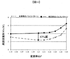
本実施例の効果を図14に示す。ここで,高調波損失Whは,(数7)に基づいて,損失係数λ=0.5として計算している。また,高調波次数nが200より大きい次数の高調波損失は,0と仮定している。図14に示す通り,本発明のパルスパターンは,補正前のパルスパターンに比べ,高調波損失Whを低減できており,その低減量は,最大で43%である。
The effect of this example is shown in FIG. Here, the harmonic loss Wh is calculated based on (Equation 7) with a loss coefficient λ = 0.5. In addition, it is assumed that the harmonic loss of the harmonic order n greater than 200 is zero. As shown in FIG. 14, the pulse pattern of the present invention can reduce the harmonic loss Wh compared with the pulse pattern before correction, and the reduction amount is 43% at the maximum.
図15は,実施例2の構成図であり,図21はその要素である。ただし,実施例1と同等の点については省略する。
FIG. 15 is a block diagram of the second embodiment, and FIG. 21 shows its elements. However, the same points as in Example 1 are omitted.
キャリア波生成部3は,キャリア周波数fc*に基づいてキャリア波Vc*を出力する。非同期補正位相演算部16は,ベース数Bおよびパルス数Pnに基づいて,第二ゼロ保持位相β02,第二ゼロクロス位相β12および第二ピーク位相β22を演算する。
The carrier wave generator 3 outputs a carrier wave Vc * based on the carrier frequency fc *. The asynchronous correction phase calculator 16 calculates the second zero hold phase β02, the second zero cross phase β12, and the second peak phase β22 based on the base number B and the pulse number Pn.
補正信号生成部13は,第二ゼロ保持位相β02,第二ゼロクロス位相β12,第二ピーク位相β22,ゼロクロス補正量A1,ピーク補正量Amおよび電圧位相θ*に基づいて,非同期補正信号A2を生成する。
The correction signal generator 13 generates an asynchronous correction signal A2 based on the second zero hold phase β02, the second zero cross phase β12, the second peak phase β22, the zero cross correction amount A1, the peak correction amount Am, and the voltage phase θ *. To do.
以上が,実施例2の構成である。次に,実施例2の内容について説明する。
The above is the configuration of the second embodiment. Next, the contents of the second embodiment will be described.
実施例2では,非同期PWM制御における過変調域の高調波損失を低減する。非同期PWM制御では,キャリア周波数fc*を基本波周波数f1*に依らず固定とする。このため,キャリア波Vc*と信号波Vu*の符号が切り替わるゼロクロス点は,図16のBに示す通り,一致しない。非同期PWM制御において,パルス電圧Vuは,信号波Vu*とキャリア波Vc*のゼロクロス点が一致しないため,信号の周期T1に対して非周期波形となる。ただし,図17に示す通り,信号波の周期T1と,キャリア波の周期Tcの最小公倍数である周期Tに対して周期波形となる。よって,実施例2では,高調波電圧Vnを最小公倍周期Tを基準に(数18)の通り求める。
In Example 2, harmonic loss in the overmodulation region in asynchronous PWM control is reduced. In asynchronous PWM control, the carrier frequency fc * is fixed regardless of the fundamental frequency f1 *. For this reason, the zero cross points at which the signs of the carrier wave Vc * and the signal wave Vu * are switched do not match as shown in B of FIG. In the asynchronous PWM control, the pulse voltage Vu has an aperiodic waveform with respect to the signal cycle T1 because the zero-cross points of the signal wave Vu * and the carrier wave Vc * do not match. However, as shown in FIG. 17, the waveform is a periodic waveform with respect to the period T1 which is the least common multiple of the period T1 of the signal wave and the period Tc of the carrier wave. Therefore, in the second embodiment, the harmonic voltage Vn is obtained as (Equation 18) based on the least common period T.

よって,非同期PWM制御では,図16(b)に示す通り,基本波成分より低域にも高調波成分が発生する。制御角αは,(数18)を(数6)に代入して得られる(数19)を低減あるいは最小化するように演算される。また,(数19の拘束条件である変調率Kh*は,1.2に固定して演算される。
Therefore, in asynchronous PWM control, as shown in Fig. 16 (b), harmonic components are also generated in the lower region than the fundamental component. The control angle α is calculated so as to reduce or minimize (Equation 19) obtained by substituting (Equation 18) into (Equation 6). Also, the modulation factor Kh *, which is the constraint condition of Equation (19), is calculated with being fixed at 1.2.

図18に実施例2の効果を示す。図18(a)および図18(b)では,従来手法と本発明において,電圧高調波Vnの実効値が等しいにも関わらず,高調波損失Whを低減できている。また,図18(c)および図18(d)において,電圧高調波Vnの実効値が増加しているにも関わらず,高調波損失Whを低減できる。
Fig. 18 shows the effect of Example 2. 18 (a) and 18 (b), the harmonic loss Wh can be reduced in the conventional method and the present invention even though the effective value of the voltage harmonic Vn is equal. In FIGS. 18 (c) and 18 (d), the harmonic loss Wh can be reduced despite the increase in the effective value of the voltage harmonic Vn.
図19は,実施例3の構成図であり,実施例1もしくは実施例2を搭載し,交流モータ1を駆動する駆動システムである。
FIG. 19 is a configuration diagram of the third embodiment, and shows a drive system that mounts the first or second embodiment and drives the AC motor 1.
実施例3では,コンピュータ17などの上位装置からトルク指令τ*もしくは周波数指令f*が出力される。
In Example 3, a torque command τ * or a frequency command f * is output from a host device such as the computer 17.
V/f制御部18およびベクトル制御部19は,トルク指令τ*あるいは周波数指令f*を基に基本波周波数f1*と変調率Kh*を演算する。
The V / f control unit 18 and the vector control unit 19 calculate the fundamental frequency f1 * and the modulation factor Kh * based on the torque command τ * or the frequency command f *.
制御モード変換部20は,トルク指令τ*と周波数指令f*を切り替える。制御選択部21は,V/f制御部18とベクトル制御部19を切り替える。
The control mode conversion unit 20 switches between the torque command τ * and the frequency command f *. The control selection unit 21 switches between the V / f control unit 18 and the vector control unit 19.
位相演算部22は,基本波周波数f1*に基いて電圧位相θ*を演算する。実施例3で演算された基本波周波数f1*,電圧位相θ*および変調率Kh*は,実施例1もしくは実施例2のモータ制御装置に出力され,交流モータ1が駆動する。
The phase calculation unit 22 calculates the voltage phase θ * based on the fundamental frequency f1 *. The fundamental frequency f1 *, voltage phase θ *, and modulation factor Kh * calculated in the third embodiment are output to the motor control device of the first or second embodiment, and the AC motor 1 is driven.
本実施例により,指令値をトルク指令τ*もしくは周波数指令f*およびベクトル制御部19もしくはV/f制御部18を任意に設定できる。
According to this embodiment, the command value can be arbitrarily set in the torque command τ * or the frequency command f * and the vector control unit 19 or the V / f control unit 18.
1…交流モータ
2…インバータ
3…周波数演算部
4…周波数補正部
5…第一変調モード判定部
6…キャリア波生成部
7…振幅演算部
8…第二変調モード判定部
9…信号波生成部
10…補正量演算部
10a…制御角演算部
10b…ピーク補正量演算部
10c…ゼロクロス正量演算部
11…パターン判定部
12…同期補正位相演算部
13…補正信号生成部
14…第三変調モード判定部
15…PWM制御部
16…非同期補正位相演算部
17…コンピュータ
18…V/f制御部
19…ベクトル制御部
20…制御モード切り替え部
21…制御選択部
22…位相演算部
VDC…直流電圧
Vu,Vv,Vw…U相パルス電圧,V相パルス電圧,W相パルス電圧
Iu,Iv,Iw…U相電流,V相電流,W相電流
Vu*,Vv*,Vw*…U相信号波,V相信号波,W相信号波
Vu2*,Vv2*,Vw2*…U相補正信号波,V相補正信号波,W相補正信号波
Vuv…線間電圧
Vc*…キャリア波
P…パターン
A…同期補正信号,A*…最終補正信号
A1…ゼロクロス補正量
Am…ピーク補正量
Vn…高調波電圧
Guu,Gup…U相ゲート信号
Gvu,Gvp…V相ゲート信号
Gwu,Gwp…W相ゲート信号
θ*…電圧位相
f*…周波数指令
τ*…トルク指令
Kh*…変調率
f1*…基本波周波数
fc**…最終キャリア波周波数
fc*…キャリア波周波数
fc2*…補正キャリア波周波数
Tc…キャリア波周期
T1…信号波周期
T…キャリア波と信号波の最小公倍周期
In…高調波電流
Z…交流モータのインピーダンス
L…交流モータのインダクタンス
λ…損失係数
n…高調波次数
Wh…高調波損失
α…制御角
β0…ゼロ保持位相
β1…ゼロクロス位相
β2…ピーク位相
β02…第二ゼロ保持位相
β12…第二ゼロクロス位相
β22…第二ピーク位相
Amp1…第一振幅
Amp2…固定振幅
Amp…最終振幅
fcmax…最大キャリア周波数
Pn…パルス数 1 ...AC motor 2 ... Inverter 3 ... Frequency calculation unit 4 ... Frequency correction unit 5 ... First modulation mode determination unit 6 ... Carrier wave generation unit 7 ... Amplitude calculation unit 8 ... Second modulation mode determination unit 9 ... Signal wave generation unit 10 ... Correction amount calculation unit 10a ... Control angle calculation unit 10b ... Peak correction amount calculation unit 10c ... Zero cross positive amount calculation unit 11 ... Pattern determination unit 12 ... Synchronization correction phase calculation unit 13 ... Correction signal generation unit 14 ... Third modulation mode Determination unit 15 ... PWM control unit 16 ... Asynchronous correction phase calculation unit 17 ... Computer 18 ... V / f control unit 19 ... Vector control unit 20 ... Control mode switching unit 21 ... Control selection unit 22 ... Phase calculation unit VDC ... DC voltage Vu , Vv, Vw… U phase pulse voltage, V phase pulse voltage, W phase pulse voltage Iu, Iv, Iw… U phase current, V phase current, W phase current Vu *, Vv *, Vw *… U phase signal wave, V phase signal wave, W phase signal wave Vu2 *, Vv2 *, Vw2 * ... U phase correction signal wave, V phase correction signal wave, W phase correction signal wave Vuv ... Line voltage Vc * ... Carrier wave P ... Pattern A ... Synchronization correction signal, A * ... Final correction signal A1 ... Zero cross correction amount Am ... Peak correction amount Vn ... Harmonic voltage Guu, Gup ... U phase gate signal
Gvu, Gvp ... V-phase gate signal Gwu, Gwp ... W-phase gate signal θ * ... Voltage phase f * ... Frequency command τ * ... Torque command Kh * ... Modulation rate f1 * ... Fundamental frequency fc ** ... Final carrier wave frequency fc * ... carrier wave frequency fc2 * ... corrected carrier wave frequency Tc ... carrier wave period T1 ... signal wave period T ... least common frequency of carrier wave and signal wave In ... harmonic current Z ... AC motor impedance L ... AC motor Inductance λ ... loss factor n ... harmonic order Wh ... harmonic loss α ... control angle β0 ... zero hold phase β1 ... zero cross phase β2 ... peak phase β02 ... second zero hold phase β12 ... second zero cross phase β22 ... second Peak phase Amp1… First amplitude Amp2… Fixed amplitude Amp… Final amplitude fcmax… Maximum carrier frequency Pn… Number of pulses
2…インバータ
3…周波数演算部
4…周波数補正部
5…第一変調モード判定部
6…キャリア波生成部
7…振幅演算部
8…第二変調モード判定部
9…信号波生成部
10…補正量演算部
10a…制御角演算部
10b…ピーク補正量演算部
10c…ゼロクロス正量演算部
11…パターン判定部
12…同期補正位相演算部
13…補正信号生成部
14…第三変調モード判定部
15…PWM制御部
16…非同期補正位相演算部
17…コンピュータ
18…V/f制御部
19…ベクトル制御部
20…制御モード切り替え部
21…制御選択部
22…位相演算部
VDC…直流電圧
Vu,Vv,Vw…U相パルス電圧,V相パルス電圧,W相パルス電圧
Iu,Iv,Iw…U相電流,V相電流,W相電流
Vu*,Vv*,Vw*…U相信号波,V相信号波,W相信号波
Vu2*,Vv2*,Vw2*…U相補正信号波,V相補正信号波,W相補正信号波
Vuv…線間電圧
Vc*…キャリア波
P…パターン
A…同期補正信号,A*…最終補正信号
A1…ゼロクロス補正量
Am…ピーク補正量
Vn…高調波電圧
Guu,Gup…U相ゲート信号
Gvu,Gvp…V相ゲート信号
Gwu,Gwp…W相ゲート信号
θ*…電圧位相
f*…周波数指令
τ*…トルク指令
Kh*…変調率
f1*…基本波周波数
fc**…最終キャリア波周波数
fc*…キャリア波周波数
fc2*…補正キャリア波周波数
Tc…キャリア波周期
T1…信号波周期
T…キャリア波と信号波の最小公倍周期
In…高調波電流
Z…交流モータのインピーダンス
L…交流モータのインダクタンス
λ…損失係数
n…高調波次数
Wh…高調波損失
α…制御角
β0…ゼロ保持位相
β1…ゼロクロス位相
β2…ピーク位相
β02…第二ゼロ保持位相
β12…第二ゼロクロス位相
β22…第二ピーク位相
Amp1…第一振幅
Amp2…固定振幅
Amp…最終振幅
fcmax…最大キャリア周波数
Pn…パルス数 1 ...
Gvu, Gvp ... V-phase gate signal Gwu, Gwp ... W-phase gate signal θ * ... Voltage phase f * ... Frequency command τ * ... Torque command Kh * ... Modulation rate f1 * ... Fundamental frequency fc ** ... Final carrier wave frequency fc * ... carrier wave frequency fc2 * ... corrected carrier wave frequency Tc ... carrier wave period T1 ... signal wave period T ... least common frequency of carrier wave and signal wave In ... harmonic current Z ... AC motor impedance L ... AC motor Inductance λ ... loss factor n ... harmonic order Wh ... harmonic loss α ... control angle β0 ... zero hold phase β1 ... zero cross phase β2 ... peak phase β02 ... second zero hold phase β12 ... second zero cross phase β22 ... second Peak phase Amp1… First amplitude Amp2… Fixed amplitude Amp… Final amplitude fcmax… Maximum carrier frequency Pn… Number of pulses
Claims (9)
- 直流電圧によって正規化される変調率に基づいて第一振幅を演算する振幅演算部と、
電圧位相および前記第一振幅に基づいて信号波を生成する信号波生成部と、
基本波周波数に基づいてベース数およびキャリア周波数を演算する周波数演算部と、
前記キャリア周波数に基づいてキャリア波を生成するキャリア波生成部と、
前記信号波と前記キャリア波を比較し,ゲート信号を出力するPWM制御部と、
前記ゲート信号に基づいてスイッチング素子を制御し,パルス電圧を出力するインバータと、を備えるモータ制御装置において,
前記キャリア周波数と前記基本波周波数の比であるベース数およびパターンに基づいて補正キャリア周波数を演算する周波数補正部と、
前記ベース数に基づいて前記パターンを演算するパターン判定部と、
前記変調率が1以上の所定の値に達した場合,最終キャリア周波数を前記キャリア周波数から前記補正キャリア周波数に切り換える第一変調モード判定部と、
前記変調率,前記電圧位相および前記ベース数に基づいてパルス数,ゼロクロス補正量およびピーク補正量を演算する補正量演算部と、
前記パルス数と前記補正キャリア周波数と前記パターンおよび前記基本波周波数に基づいてゼロ保持位相,ゼロクロス位相およびピーク位相を演算する同期補正位相演算部と、
前記ゼロ保持位相,前記ゼロクロス位相,前記ピーク位相,前記ピーク補正量,前記ゼロクロス補正量および前記電圧位相に基づいて同期補正信号を生成する補正信号生成部と、
前記変調率が1以上の所定の値に達した場合,最終補正信号波を0から前記同期補正信号に切り換える第二変調モード判定部と、
前記変調率が1以上の所定の値に達した場合,最終振幅を前記第一振幅から固定振幅に切り換える第三変調モード判定部と、を備えることを特徴とするモータ制御装置。 An amplitude calculator that calculates the first amplitude based on the modulation rate normalized by the DC voltage;
A signal wave generator that generates a signal wave based on the voltage phase and the first amplitude;
A frequency calculator that calculates the number of bases and the carrier frequency based on the fundamental frequency;
A carrier wave generator for generating a carrier wave based on the carrier frequency;
A PWM controller that compares the signal wave with the carrier wave and outputs a gate signal;
In a motor control device comprising: an inverter that controls a switching element based on the gate signal and outputs a pulse voltage;
A frequency correction unit that calculates a correction carrier frequency based on a base number and a pattern that is a ratio of the carrier frequency and the fundamental frequency;
A pattern determination unit that calculates the pattern based on the base number;
A first modulation mode determination unit that switches a final carrier frequency from the carrier frequency to the corrected carrier frequency when the modulation rate reaches a predetermined value of 1 or more;
A correction amount calculator that calculates the number of pulses, the zero-cross correction amount, and the peak correction amount based on the modulation factor, the voltage phase, and the base number;
A synchronization correction phase calculator that calculates a zero hold phase, a zero cross phase, and a peak phase based on the number of pulses, the correction carrier frequency, the pattern, and the fundamental frequency;
A correction signal generator that generates a synchronization correction signal based on the zero hold phase, the zero cross phase, the peak phase, the peak correction amount, the zero cross correction amount, and the voltage phase;
A second modulation mode determination unit that switches a final correction signal wave from 0 to the synchronization correction signal when the modulation rate reaches a predetermined value of 1 or more;
A motor control device comprising: a third modulation mode determination unit that switches a final amplitude from the first amplitude to a fixed amplitude when the modulation rate reaches a predetermined value of 1 or more. - 請求項1に記載するモータ制御装置において,
前記補正量演算部は,
前記変調率と前記ベース数に基づいて,前記パルス数および,下記数式の高調波損失を低減あるいは最小化するような前記制御角を演算する制御角演算部と、
前記ベース数に基づいて前記パターンを判定する第二パターン判定部と、
前記パルス数と前記制御角と前記変調率に基づいて前記ゼロクロス補正量を演算するゼロクロス補正量演算部と、
前記変調率に基づいて前記ピーク量補正部を演算するピーク補正量演算部と、を備えることを特徴とするモータ制御装置。

The correction amount calculation unit
Based on the modulation factor and the base number, a control angle calculation unit that calculates the control angle so as to reduce or minimize the number of pulses and the harmonic loss of the following equation;
A second pattern determination unit that determines the pattern based on the base number;
A zero-cross correction amount calculation unit that calculates the zero-cross correction amount based on the number of pulses, the control angle, and the modulation rate;
A motor control apparatus comprising: a peak correction amount calculation unit that calculates the peak amount correction unit based on the modulation rate.
- 請求項1に記載するモータ制御装置において,
前記ゼロクロス補正位相は,前記パルス電圧が前記電圧位相0,180degから各々±38deg以内でオン動作およびオフ動作するように演算され,
前記ピーク補正位相は,前記電圧位相90,270degから各々±5deg以内でオフ動作するように演算されることを特徴とするモータ制御装置。 In the motor control device according to claim 1,
The zero-cross correction phase is calculated so that the pulse voltage is turned on and off within ± 38 deg from the voltage phase 0,180 deg,
The motor control device according to claim 1, wherein the peak correction phase is calculated so as to be turned off within ± 5 deg from the voltage phase 90, 270 deg. - 請求項1に記載するモータ制御装置において,
前記ゼロクロス補正量は,前記変調率が1.22より小さい場合,前記変調率が変化しても前記変調率に依らず演算され,
前記電圧位相0,180degから各々±38deg以内の領域で前記パルス電圧がオン動作およびオフ動作するタイミングが一致するように演算されることを特徴とするモータ制御装置。 In the motor control device according to claim 1,
The zero-cross correction amount is calculated regardless of the modulation rate even if the modulation rate is changed when the modulation rate is smaller than 1.22.
The motor control device according to claim 1, wherein the pulse voltage is calculated so that the timings at which the pulse voltage is turned on and off in a region within ± 38 deg from each of the voltage phases 0 and 180 deg. - 請求項1に記載するモータ制御装置において,
前記ピーク補正量は,前記変調率が1.22より小さい場合,前記変調率に基づいて,前記パルス電圧が前記電圧位相90,270degから各々±5deg以内でオフ動作するように演算されることを特徴とするモータ制御装置。 In the motor control device according to claim 1,
The peak correction amount is calculated such that when the modulation rate is smaller than 1.22, the pulse voltage is turned off within ± 5 deg from the voltage phase 90, 270 deg based on the modulation rate. Motor control device. - 請求項1に記載するモータ制御装置において,
前記ゼロクロス補正量は,前記変調率が1.22より大きい場合,前記変調率に基づいて演算され,
前記ピーク補正量は,1に設定されることを特徴とするモータ制御装置。 In the motor control device according to claim 1,
The zero cross correction amount is calculated based on the modulation rate when the modulation rate is greater than 1.22,
The motor controller according to claim 1, wherein the peak correction amount is set to 1. - 請求項1に記載するモータ制御装置において,
前記キャリア波が前記基本波周波数に依らず固定値である場合,
前記ベース数および前記パルス数Pnに基づいて,第二ゼロ保持位相β02,第二ゼロクロス位相β12および第二ピーク位相β22を演算する非同期補正位相演算部16を備え,
前記第二ゼロ保持位相,前記第二ゼロクロス位相,前記第二ピーク位相β22,前記ゼロクロス補正量A1,前記ピーク補正量Amおよび電圧位相θ*に基づいて,非同期補正信号を生成する補正信号生成部を備えることを特徴とするモータ制御装置。 In the motor control device according to claim 1,
When the carrier wave is a fixed value regardless of the fundamental frequency,
Based on the base number and the pulse number Pn, an asynchronous correction phase calculator 16 for calculating a second zero holding phase β02, a second zero cross phase β12, and a second peak phase β22,
A correction signal generator that generates an asynchronous correction signal based on the second zero hold phase, the second zero cross phase, the second peak phase β22, the zero cross correction amount A1, the peak correction amount Am, and the voltage phase θ *. A motor control device comprising: - 請求項7に記載するモータ制御装置において,前記制御角は,前記信号波の周期と前記キャリア波の周期の最小公倍周期を基準とした下記数式を低減あるいは最小化するように演算されることを特徴とするモータ制御装置。

- 請求項1~請求項8のいずれか1項に記載するモータ制御装置を備え,
トルク指令あるいは周波数指令に基づいて前記基本波周波数および前記変調率を演算するベクトル制御部およびV/f制御部と、
前記ベクトル制御部と前記V/f制御部を切り換える制御選択部と、
前記トルク指令および前記周波数指令を切り換える制御モード切り替え部と、
前記基本波周波数に基づいて前記電圧位相を演算する位相演算部と、を備えることを特徴とするモータ駆動システム。 A motor control device according to any one of claims 1 to 8, comprising:
A vector control unit and a V / f control unit for calculating the fundamental frequency and the modulation factor based on a torque command or a frequency command;
A control selection unit that switches between the vector control unit and the V / f control unit;
A control mode switching unit that switches between the torque command and the frequency command;
And a phase calculator that calculates the voltage phase based on the fundamental frequency.
Priority Applications (2)
| Application Number | Priority Date | Filing Date | Title |
|---|---|---|---|
| EP17766080.0A EP3432467B1 (en) | 2016-03-15 | 2017-01-30 | Motor control device and drive system |
| CN201780007490.XA CN108476011B (en) | 2016-03-15 | 2017-01-30 | Motor control device and drive system |
Applications Claiming Priority (2)
| Application Number | Priority Date | Filing Date | Title |
|---|---|---|---|
| JP2016-050388 | 2016-03-15 | ||
| JP2016050388A JP6674804B2 (en) | 2016-03-15 | 2016-03-15 | Motor control device and drive system |
Publications (1)
| Publication Number | Publication Date |
|---|---|
| WO2017159072A1 true WO2017159072A1 (en) | 2017-09-21 |
Family
ID=59852256
Family Applications (1)
| Application Number | Title | Priority Date | Filing Date |
|---|---|---|---|
| PCT/JP2017/003085 WO2017159072A1 (en) | 2016-03-15 | 2017-01-30 | Motor control device and drive system |
Country Status (4)
| Country | Link |
|---|---|
| EP (1) | EP3432467B1 (en) |
| JP (1) | JP6674804B2 (en) |
| CN (1) | CN108476011B (en) |
| WO (1) | WO2017159072A1 (en) |
Cited By (1)
| Publication number | Priority date | Publication date | Assignee | Title |
|---|---|---|---|---|
| CN111342726A (en) * | 2020-03-26 | 2020-06-26 | 武汉科技大学 | Direct torque control method and system for permanent magnet synchronous motor |
Families Citing this family (2)
| Publication number | Priority date | Publication date | Assignee | Title |
|---|---|---|---|---|
| CN111585499B (en) * | 2019-02-18 | 2023-07-21 | 本田技研工业株式会社 | Control device, vehicle system, and control method |
| JP6989574B2 (en) | 2019-09-25 | 2022-01-05 | 本田技研工業株式会社 | Control device, vehicle system and control method |
Citations (5)
| Publication number | Priority date | Publication date | Assignee | Title |
|---|---|---|---|---|
| JP2007143316A (en) * | 2005-11-18 | 2007-06-07 | Mitsubishi Electric Corp | Motor controller |
| JP2013141336A (en) * | 2011-12-28 | 2013-07-18 | Hitachi Appliances Inc | Motor control device and air conditioner |
| JP2014072936A (en) * | 2012-09-28 | 2014-04-21 | Hitachi Ltd | Ac motor drive system and motor vehicle |
| JP2015053824A (en) | 2013-09-09 | 2015-03-19 | 株式会社日立製作所 | Motor drive system, and electric railway vehicle mounting the same |
| JP2016005378A (en) * | 2014-06-18 | 2016-01-12 | 株式会社日立製作所 | Inverter and drive system employing the same |
Family Cites Families (2)
| Publication number | Priority date | Publication date | Assignee | Title |
|---|---|---|---|---|
| JP4858597B2 (en) * | 2008-11-28 | 2012-01-18 | 株式会社デンソー | Rotating machine control device and manufacturing method thereof |
| JP4911241B1 (en) * | 2010-11-16 | 2012-04-04 | ダイキン工業株式会社 | Power converter |
-
2016
- 2016-03-15 JP JP2016050388A patent/JP6674804B2/en active Active
-
2017
- 2017-01-30 WO PCT/JP2017/003085 patent/WO2017159072A1/en active Application Filing
- 2017-01-30 EP EP17766080.0A patent/EP3432467B1/en active Active
- 2017-01-30 CN CN201780007490.XA patent/CN108476011B/en not_active Expired - Fee Related
Patent Citations (5)
| Publication number | Priority date | Publication date | Assignee | Title |
|---|---|---|---|---|
| JP2007143316A (en) * | 2005-11-18 | 2007-06-07 | Mitsubishi Electric Corp | Motor controller |
| JP2013141336A (en) * | 2011-12-28 | 2013-07-18 | Hitachi Appliances Inc | Motor control device and air conditioner |
| JP2014072936A (en) * | 2012-09-28 | 2014-04-21 | Hitachi Ltd | Ac motor drive system and motor vehicle |
| JP2015053824A (en) | 2013-09-09 | 2015-03-19 | 株式会社日立製作所 | Motor drive system, and electric railway vehicle mounting the same |
| JP2016005378A (en) * | 2014-06-18 | 2016-01-12 | 株式会社日立製作所 | Inverter and drive system employing the same |
Non-Patent Citations (1)
| Title |
|---|
| See also references of EP3432467A4 |
Cited By (2)
| Publication number | Priority date | Publication date | Assignee | Title |
|---|---|---|---|---|
| CN111342726A (en) * | 2020-03-26 | 2020-06-26 | 武汉科技大学 | Direct torque control method and system for permanent magnet synchronous motor |
| CN111342726B (en) * | 2020-03-26 | 2023-05-30 | 武汉科技大学 | Direct torque control method and system for permanent magnet synchronous motor |
Also Published As
| Publication number | Publication date |
|---|---|
| EP3432467A1 (en) | 2019-01-23 |
| JP6674804B2 (en) | 2020-04-01 |
| EP3432467A4 (en) | 2019-10-23 |
| CN108476011A (en) | 2018-08-31 |
| JP2017169295A (en) | 2017-09-21 |
| CN108476011B (en) | 2021-05-28 |
| EP3432467B1 (en) | 2022-04-06 |
Similar Documents
| Publication | Publication Date | Title |
|---|---|---|
| JP5866065B2 (en) | AC motor control device | |
| JP6566105B2 (en) | Power converter | |
| WO2014196013A1 (en) | Power conversion device | |
| Videt et al. | PWM strategy for the cancellation of common-mode voltage generated by three-phase back-to-back inverters | |
| EP3528383A1 (en) | Control device and control method for alternating current motor, and alternating current motor driving system | |
| WO2015115223A1 (en) | Inverter control method and voltage-type inverter | |
| JP6239448B2 (en) | Inverter and drive system using the same | |
| WO2017119214A1 (en) | Electric power converting device | |
| WO2017159072A1 (en) | Motor control device and drive system | |
| WO2016152250A1 (en) | Motor control device | |
| Mink et al. | Feedback control of high-speed PMSM with synchronous optimal PWM | |
| JP2017093077A (en) | Controller and control method of open winding system | |
| JP2008048530A (en) | Spatial vector modulation method of ac-ac direct converter | |
| JP4893152B2 (en) | Space vector modulation method for AC-AC direct conversion device | |
| JP2007116856A (en) | Power conversion device | |
| WO2015125540A1 (en) | Inverter control method and inverter | |
| Corzine et al. | Distributed control of hybrid motor drives | |
| JP5761095B2 (en) | Rotating machine control device | |
| Holagh et al. | Improved selective harmonic elimination for reducing torque harmonics of induction motors in wide DC bus voltage variations | |
| JP2006280063A (en) | Controller of ac/ac direct power converter | |
| Mirazimi et al. | Space vector PWM method for two-phase three-leg inverters | |
| Nishizawa et al. | Reduction of dc-link current harmonics over wide power-factor range for three-phase VSI using single-carrier-comparison continuous PWM | |
| JP4905174B2 (en) | AC / AC direct converter controller | |
| JP2006141175A (en) | Motor control device of ac-ac direct converter | |
| JP2014039425A (en) | Pwm voltage generating device for inverter |
Legal Events
| Date | Code | Title | Description |
|---|---|---|---|
| NENP | Non-entry into the national phase |
Ref country code: DE |
|
| 121 | Ep: the epo has been informed by wipo that ep was designated in this application |
Ref document number: 17766080 Country of ref document: EP Kind code of ref document: A1 |
|
| WWE | Wipo information: entry into national phase |
Ref document number: 2017766080 Country of ref document: EP |
|
| ENP | Entry into the national phase |
Ref document number: 2017766080 Country of ref document: EP Effective date: 20181015 |