EP3432467A1 - Motor control device and drive system - Google Patents
Motor control device and drive system Download PDFInfo
- Publication number
- EP3432467A1 EP3432467A1 EP17766080.0A EP17766080A EP3432467A1 EP 3432467 A1 EP3432467 A1 EP 3432467A1 EP 17766080 A EP17766080 A EP 17766080A EP 3432467 A1 EP3432467 A1 EP 3432467A1
- Authority
- EP
- European Patent Office
- Prior art keywords
- phase
- basis
- zero
- voltage
- modulation rate
- Prior art date
- Legal status (The legal status is an assumption and is not a legal conclusion. Google has not performed a legal analysis and makes no representation as to the accuracy of the status listed.)
- Granted
Links
- 230000001360 synchronised effect Effects 0.000 claims abstract description 22
- 230000007274 generation of a signal involved in cell-cell signaling Effects 0.000 claims description 6
- 238000010586 diagram Methods 0.000 description 12
- 230000000694 effects Effects 0.000 description 8
- 238000000034 method Methods 0.000 description 4
- 238000005457 optimization Methods 0.000 description 4
- 238000007796 conventional method Methods 0.000 description 3
- RYGMFSIKBFXOCR-UHFFFAOYSA-N Copper Chemical compound [Cu] RYGMFSIKBFXOCR-UHFFFAOYSA-N 0.000 description 2
- 229910052802 copper Inorganic materials 0.000 description 2
- 239000010949 copper Substances 0.000 description 2
- 230000000737 periodic effect Effects 0.000 description 2
- 229910000831 Steel Inorganic materials 0.000 description 1
- 238000001816 cooling Methods 0.000 description 1
- 238000010606 normalization Methods 0.000 description 1
- 239000010959 steel Substances 0.000 description 1
Images


Classifications
-
- H—ELECTRICITY
- H02—GENERATION; CONVERSION OR DISTRIBUTION OF ELECTRIC POWER
- H02P—CONTROL OR REGULATION OF ELECTRIC MOTORS, ELECTRIC GENERATORS OR DYNAMO-ELECTRIC CONVERTERS; CONTROLLING TRANSFORMERS, REACTORS OR CHOKE COILS
- H02P27/00—Arrangements or methods for the control of AC motors characterised by the kind of supply voltage
- H02P27/04—Arrangements or methods for the control of AC motors characterised by the kind of supply voltage using variable-frequency supply voltage, e.g. inverter or converter supply voltage
- H02P27/06—Arrangements or methods for the control of AC motors characterised by the kind of supply voltage using variable-frequency supply voltage, e.g. inverter or converter supply voltage using dc to ac converters or inverters
- H02P27/08—Arrangements or methods for the control of AC motors characterised by the kind of supply voltage using variable-frequency supply voltage, e.g. inverter or converter supply voltage using dc to ac converters or inverters with pulse width modulation
-
- H—ELECTRICITY
- H02—GENERATION; CONVERSION OR DISTRIBUTION OF ELECTRIC POWER
- H02P—CONTROL OR REGULATION OF ELECTRIC MOTORS, ELECTRIC GENERATORS OR DYNAMO-ELECTRIC CONVERTERS; CONTROLLING TRANSFORMERS, REACTORS OR CHOKE COILS
- H02P21/00—Arrangements or methods for the control of electric machines by vector control, e.g. by control of field orientation
-
- H—ELECTRICITY
- H02—GENERATION; CONVERSION OR DISTRIBUTION OF ELECTRIC POWER
- H02P—CONTROL OR REGULATION OF ELECTRIC MOTORS, ELECTRIC GENERATORS OR DYNAMO-ELECTRIC CONVERTERS; CONTROLLING TRANSFORMERS, REACTORS OR CHOKE COILS
- H02P27/00—Arrangements or methods for the control of AC motors characterised by the kind of supply voltage
- H02P27/04—Arrangements or methods for the control of AC motors characterised by the kind of supply voltage using variable-frequency supply voltage, e.g. inverter or converter supply voltage
-
- H—ELECTRICITY
- H02—GENERATION; CONVERSION OR DISTRIBUTION OF ELECTRIC POWER
- H02P—CONTROL OR REGULATION OF ELECTRIC MOTORS, ELECTRIC GENERATORS OR DYNAMO-ELECTRIC CONVERTERS; CONTROLLING TRANSFORMERS, REACTORS OR CHOKE COILS
- H02P2209/00—Indexing scheme relating to controlling arrangements characterised by the waveform of the supplied voltage or current
- H02P2209/09—PWM with fixed limited number of pulses per period
Landscapes
- Engineering & Computer Science (AREA)
- Power Engineering (AREA)
- Control Of Ac Motors In General (AREA)
- Inverter Devices (AREA)
Abstract
Description
- The present invention relates to a motor control device and a drive system to reduce a harmonic loss.
- A motor drive system by a PWM control used in an inverter is desired to reduce various types of losses. The losses are classified into a loss occurring in a motor (hereinafter, referred to as motor loss) and a loss occurring in the inverter (hereinafter, referred to as inverter loss). The motor loss includes a loss caused by a fundamental component (hereinafter, referred to as fundamental wave loss) and a loss caused by harmonic components (hereinafter, referred to as harmonic loss) . The inverter loss includes a loss caused by an ON/OFF operation of a switching element (hereinafter, referred to as switching loss) and a loss occurring when the switching element is conducting (hereinafter, referred to as conduction loss).
- The fundamental wave loss is reduced by employing a variable speed drive using the inverter compared to a constant speed drive using a commercial power source. However, the switching operation causes a distortion in voltage and current, and generates harmonic components. Therefore, the harmonic loss is increased. The harmonic components and the harmonic loss can be reduced by increasing a carrier frequency of the inverter. However, the switching loss is increased at the same time. Therefore, the harmonic loss is desired to be reduced without increasing the carrier frequency. In particular, it has been known that the harmonic components and the harmonic loss are apparently increased when the motor is driven in an over-modulation region, and thus it is desired to reduce the harmonic components and the harmonic loss.
-
PTL 1 is a technique of a synchronous PWM control for a railway system, in which a pulse voltage is turned on or off one or more times near zero-cross points (0 and 180 deg) and peak points (90 and 270 deg) of a fundamental wave phase in order to reduce the harmonic loss which is caused in the over-modulation region, and an on or off state is held in other phase regions. - PTL 1:
JP 2015-053824 A - Problems of
PTL 1 are that as the technique is a method for the synchronous PWM control, it does not cope with an asynchronous PWM control, and that as the technique is for the railway system, an upper limit of the carrier frequency is low, and the effect can be achieved only in a narrow range of drive region. - In order to reduce the harmonic loss of the over-modulation region and to widen a drive range showing the effect, there is a need to cope with the asynchronous PWM control and to increase the upper limit of the carrier frequency to a radio frequency.
- Therefore, an object of the invention is to reduce or minimize the harmonic loss which is caused when an alternating-current motor is driven in the over-modulation region.
- In order to solve the above problems, as an example of the invention, a final correction signal wave is switched from zero to the synchronous correction signal in a case where a modulation rate reaches a predetermined value equal to or greater than one, and a final amplitude is switched from the first amplitude to a fixed amplitude in a case where the modulation rate reaches a predetermined value equal to or greater than one.
- According to the invention, it is possible to reduce a harmonic loss, using an inverter, which is caused when an alternating-current motor is driven in an over-modulation region. With this configuration, it is possible to achieve effects such as a high power of the alternating-current motor or a minimization of a cooling system.
-
- [
FIG. 1] FIG. 1 is a diagram illustrating a configuration of a first embodiment of the invention. - [
FIG. 2] FIG. 2 is components of the first embodiment of the invention. - [
FIG. 3] FIG. 3 is an exemplary pulse pattern of a synchronous PWM control. - [
FIG. 4] FIG. 4 is an exemplary pulse pattern in an over-modulation region and a modulation region. - [
FIG. 5] FIG. 5 is an example of a pulse pattern of a 3rd harmonic superimposed system. - [
FIG. 6] FIG. 6 is a relation between a harmonic resistance and a harmonic number. - [
FIG. 7] FIG. 7 is a relation of a harmonic voltage to a harmonic number and a harmonic loss. - [
FIG. 8] FIG. 8 is an example of an optimized pulse pattern. - [
FIG. 9] FIG. 9 is a relation between a pulse pattern and a carrier wave. - [
FIG. 10] FIG. 10 is a pulse pattern of the 3rd harmonic superimposed system at a modulation rate Kh* 1.2, and fc* = 21f1*. - [
FIG. 11] FIG. 11 is a pulse pattern of the embodiment at the modulation rate Kh* 1.2, and fc2* = 33f1*. - [
FIG. 12] FIG. 12 is a pulse pattern of the embodiment at the modulation rate Kh* 1.15 - 1.21, and fc2* = 33f1*. - [
FIG. 13] FIG. 13 is a pulse pattern of the embodiment at the modulation rate Kh* 1.22 - 1.27, and fc2* = 33f1*. - [
FIG. 14] FIG. 14 is an effect of the first embodiment of the invention. - [
FIG. 15] FIG. 15 is a diagram illustrating a configuration of a second embodiment of the invention. - [
FIG. 16] FIG. 16 is an exemplary pulse pattern of an asynchronous PWM control. - [
FIG. 17] FIG. 17 is a reference period of the asynchronous PWM control. - [
FIG. 18] FIG. 18 is an effect of the second embodiment of the invention. - [
FIG. 19] FIG. 19 is a diagram illustrating a configuration of a third embodiment of the invention. - [
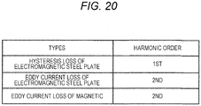
FIG. 20] FIG. 20 is a frequency dependency of the harmonic loss. - A first embodiment will be described using
FIGS. 1 to 14 , and20 . -
FIG. 1 is a diagram illustrating a configuration of a motor control device in the first embodiment, andFIG. 2 is components thereof. Aninverter 2 can control an alternating-current motor 1 by converting a DC voltage VDC into an arbitrary frequency. The alternating-current motor 1 is applied with pulse voltages (U-phase pulse voltage Vu, V-phase pulse voltage Vv, and W-phase pulse voltage Vw). Three-phase alternating currents (U-phase current Iu, V-phase current Iv, and W-phase current Iw) flow to drive the alternating-current motor 1 at a drive frequency f. Herein, a voltage applied between U-V phases of the alternating-current motor 1 is called a line voltage Vuv. - A
frequency calculation unit 3 calculates a carrier frequency fc* and a base number B on the basis of a fundamental wave frequency f1*. Herein, the base number B is a ratio of the carrier frequency fc* and the fundamental wave frequency f1*. - A
frequency correction unit 4 calculates a corrected carrier frequency fc2* on the basis of the base number B and a pattern P. - A first modulation
mode determination unit 5 switches a final carrier frequency fc2** from the carrier frequency fc* to the corrected carrier frequency fc2* when a modulation rate Kh* reaches a predetermined value equal to or greater than one. - A carrier
wave generation unit 6 outputs a carrier wave Vc* on the basis of the final carrier frequency fc**. The carrier wave Vc* is a triangular wave of amplitude "1" (normalization by DC voltage VDC/2) as illustrated inFIG. 3 , and is a function depending on a voltage phase θ*. - An
amplitude calculation unit 7 calculates a first amplitude Amp1 on the basis of the modulation rate Kh*. - A second modulation
mode determination unit 8 switches a final amplitude Amp from the first amplitude Amp1 to a fixed amplitude Amp2 when the modulation rate Kh* reaches a predetermined value equal to or greater than one. - A signal
wave generation unit 9 outputs signal waves (U-phase signal wave Vu*, V-phase signal wave Vv*, and W-phase signal wave Vw*) on the basis of the voltage phase θ* and the final amplitude Amp. The signal wave Vu* is a sinusoidal wave as illustrated inFIG. 3 , and is a function depending on the voltage phase θ*. - A correction
amount calculation unit 10 calculates a pulse number Pn, a zero-cross correction amount A1, and a peak correction amount Am on the basis of the modulation rate Kh*, the voltage phase θ*, and the base number B. - In a
pattern determination unit 11, the pattern P is determined on the basis of the base number. Herein, when the pattern P is "1," the pattern becomes a first pattern, and when P is "2," the pattern becomes a second pattern. - A synchronous correction
phase calculation unit 12 calculates a zero holding phase β0, a zero-cross phase β1, and a peak phase β2 on the basis of the pulse number Pn, the pattern P, the corrected carrier frequency fc2*, and the fundamental wave frequency f1*. Herein, the zero holding phase β0 is a phase of 1/4 period of the carrier wave Vc*. - A correction
signal generation unit 13 generates a synchronous correction signal A on the basis of the zero holding phase β0, the zero-cross phase β1, the peak phase β2, the zero-cross correction amount A1, the peak correction amount Am, and the voltage phase θ*. The synchronous correction signal A is a function depending on the voltage phase θ*. - A third modulation mode determination unit 14 switches a final correction signal A* from zero to the synchronous correction signal A when the modulation rate Kh* reaches a predetermined value equal to or greater than one.
- A
PWM control unit 15 compares correction signal waves Vu2*, Vv2*, and Vw2* obtained by adding the final correction signal A* to the signal waves Vu*, Vv*, and Vw* with the carrier wave Vc* to generate gate signals Gun, Gup, Gvn, Gvp, Gwn, and Gwv, and outputs the gate signals to theinverter 2. Theinverter 2 controls switching elements to be turned on or off on the basis of the gate signals Gun, Gup, Gvn, Gvp, Gwn, and Gwv, and applies the pulse voltages Vu, Vv, and Vw to the alternating-current motor 1. -
FIG. 2 is a diagram illustrating components of the correctionamount calculation unit 10. A controlangle calculation unit 10a calculates a control angle α and the pulse number Pn on the basis of the modulation rate Kh* and the base number B. - A peak correction
amount calculation unit 10b calculates the peak correction amount Am on the basis of the modulation rate. - A zero-cross correction
amount calculation unit 10c calculates the zero-cross correction amount A1 on the basis of the pulse number Pn and the modulation rate Kh*. - Hitherto, the diagram of the configuration and the components of the first embodiment have been described. Next, an operation principle of a PWM control will be described.
- The
PWM control unit 15 acquires the values of the signal waves Vu*, Vv*, and Vw* at every half period of the carrier wave Vc* and compares the values with the carrier wave Vc* to determine "HIGH" or "LOW" of the gate signals Gun, Gup, Gvn, Gvp, Gwn, and Gwv. Theinverter 2 outputs the pulse voltages Vu, Vv, and Vw to the alternating-current motor 1 according to "HIGH" or "LOW" of the gate signals Gun, Gup, Gvn, Gvp, Gwn, and Gwv. For example, since the signal wave Vu* is larger than the carrier wave Vc* in a section A' in a section A ofFIG. 3 , the gate signal Gup becomes high, the gate signal Gun becomes low, and the pulse voltage Vu is turned on. Therefore, one period of the carrier wave Vc* includes only one pulse of each of the pulse voltages Vu, Vv, and Vw. Hereinbelow, a waveform diagram of the pulse voltages Vu, Vv, and Vw and the voltage phase θ* is called a pulse pattern. - The PWM control includes a synchronous PWM control and an asynchronous PWM control. In the first embodiment, the description will be given about the synchronous PWM control. In the synchronous PWM control, zero-cross points at which the signs of the signal wave Vu* and the carrier wave Vc* are changed are matched as illustrated with "B" in
FIG. 3 . Therefore, the carrier frequency fc* is calculated to be an integer multiple of the fundamental wave frequency f1* by thefrequency calculation unit 3. The pulse voltage Vu becomes a periodic wave with respect to a period T1 of the signal waves Vu*, Vv*, and Vw*. In addition, the carrier frequency fc* is calculated to satisfy (Mathematical Formula 1) to keep the pulse voltages Vu, Vv, and Vw symmetrical.
[Mathematical Formula 1]
- Herein, "Pn" represents a pulse number of each of the pulse voltages Vu, Vv, and Vw of one period of the fundamental wave. For example, the pulse number Pn of the pulse pattern illustrated in
FIG. 3(a) is nine pluses. In addition, "fcmax" represents a maximum carrier frequency which can be subjected to the synchronous PWM control. For example, the maximum carrier frequency fc of a railway inverter is about several hundreds Hz, and the maximum carrier frequency fcmax of a general inverter is about several kHz. In a case where the PWM control is performed at the carrier frequency fc* higher than the maximum carrier frequency fcmax, the asynchronous PWM control is used. Hitherto, the operational principle of the PWM control has been described. - Next, the description will be given about a harmonic loss Wh which is a problem of the PWM control. In the PWM control, the voltage and the current are distorted according to the ON or OFF operation of the switching element of the
inverter 2. The distortion can be expressed as a harmonic component illustrated inFIG. 2(b) , and causes the harmonic loss Wh. In particular, when a motor is driven in an over-modulation region, the harmonic component and the harmonic loss Wh are increased apparently. The over-modulation region is a region where the modulation rate Kh* exceeds 1 (p.u.). A region where the modulation rate Kh* is less than 1 (p.u.) is called a modulation region.FIG. 4 illustrates a waveform diagram when the motor is driven in the over-modulation region (Kh = 1.24) and the modulation region (Kh = 0.6). As illustrated inFIG. 4(a) , the pulse number Pn (seven pulses) of the over-modulation region is less than the pulse number Pn (nine pulses) of the modulation region. This is because a magnitude of the signal wave Vu* near the voltage phase θ* = 90 deg illustrated in the section A ofFIG. 4 (a) is larger than the amplitude (that is, 1 p.u.) of the carrier wave Vc*. As a result, an effective value of a harmonic voltage Vn is increased, and the harmonic loss Wh is also increased. For example, as illustrated inFIG. 4(b) , a 7-th harmonic voltage Vn becomes the harmonic voltage Vn = 0.105 p.u. in a case where the motor is driven in the modulation region. On the other hand, in a case where the motor is driven in the over-modulation region, the effective value becomes the harmonic voltage Vn = 0.258 p.u., and becomes about two times compared to a case where the motor is driven in the modulation region. In addition, the effective value of a 13-th harmonic voltage Vn becomes 0.008 p.u. in a case where the motor is driven in the modulation region. In a case where the motor is driven in the over-modulation region, the effective value becomes 0.291 p.u., and becomes about 30 times compared to a case where the motor is driven in the modulation region. In this way, the amplitude of the signal wave exceeds the amplitude of the carrier wave in the over-modulation region, the effective value of the harmonic voltage Vn is increased apparently, and the harmonic loss Wh is also increased. Herein, the "harmonic voltage Vn" is an effective value of the harmonic component which is determined by the pulse pattern, depends on a phase α (hereinafter, the control angle α) where the pulse voltages Vu, Vv, and Vw are switched from on to off or from off to on, and is expressed as (Mathematical Formula 2).
[Mathematical Formula 2]
- Herein, "n" represents a harmonic number.
- In addition, the modulation rate Kh* also depends on the control angle α, and expressed as (Mathematical Formula 3).
[Mathematical Formula 3]
- Hitherto, the description has been given about the harmonic loss Wh which is a problem of the PWM control. Next, the description will be given about a conventional method of reducing the harmonic loss Wh of the over-modulation region.
- In the related art, there is used a 3rd harmonic superimposed system in which the harmonic component of three times the fundamental wave frequency f1* is superimposed on the signal waves Vu*, Vv*, and Vw*. With this regard, a system using a sinusoidal wave as the signal waves Vu*, Vv*, and Vw* is called a sinusoidal system. A waveform diagram of the 3rd harmonic superimposed system is illustrated in
FIG. 5 . The first amplitude Amp1 of the signal waves Vu*, Vv*, and Vw* in the 3rd harmonic superimposed system is calculated by (Mathematical Formula 4) on the basis of the modulation rate Kh*.
[Mathematical Formula 4]
- Herein, "Amax" represents a maximum amplitude, and "Amin" represents a minimum amplitude.
- Since superimpose the harmonic component of three times the fundamental wave frequency f1*, the magnitudes of the signal waves Vu*, Vv*, and Vw* of the voltage phase θ* = 90 deg become smaller than the amplitude (that is, 1 p.u. ) of the carrier wave Vc* even in the over-modulation region. For example, as illustrated in an enlarged portion A of
FIG. 5 , in the case of the modulation rate Kh* = 1.15, the magnitude of the signal at the voltage phase θ* = 90 deg is 0.85 p.u., and a difference with respect to the amplitude of the carrier wave Vc* becomes 0.15 p.u. Therefore, in the 3rd harmonic superimposed system, the effective value of the harmonic voltage Vn of the over-modulation region is reduced compared to the sinusoidal system. However, when the modulation rate Kh* exceeds 1.15, the magnitude of the signal wave in the section A ofFIG. 5 becomes larger than the amplitude (that is, 1 p.u.) of the carrier wave Vc*. Therefore, the effective value of the harmonic voltage Vn is increased apparently, and the harmonic loss Wh is also increased. Hitherto, the description has been given about the conventional method of reducing the harmonic loss Wh of the modulation region. Next, the description will be given about a relation between the harmonic loss Wh and the harmonic voltage Vn. - The harmonic loss Wh is a total sum of an eddy current generated in a magnet of the alternating-
current motor 1 and a hysteresis loss caused in an electromagnetic steel plate, and is proportional to a square of a harmonic current In. Herein, the harmonic current In may be expressed as (Mathematical Formula 5) using the harmonic voltage Vn of (Mathematical Formula 2).
[Mathematical Formula 5]
- Herein, "Z" represents an impedance of the alternating-
current motor 1, and "L" represents an inductance of the alternating-current motor 1. - In addition, the harmonic loss Wh is proportional to a factorial of the frequency as illustrated in
FIG. 20 which shows a frequency dependency of the harmonic loss, and is expressed as (Mathematical Formula 6).
[Mathematical Formula 6]
- Herein, "λ" represents a loss coefficient.
- Substituting (Mathematical Formula 2) into (Mathematical Formula 6), (Mathematical Formula 7) is obtained, and the harmonic loss Wh is expressed by the control angle α.
[Mathematical Formula 7]
- Herein, the loss coefficient λ is a coefficient representing a characteristic of the harmonic loss Wh of the alternating-
current motor 1, and is defined by a factor (FIG. 20 ) of the harmonic loss Wh of the alternating-current motor 1 as follows. - (1) λ = 0: No frequency dependency, and copper loss is a cause,
- (2) λ = 1: Hysteresis loss is a main cause, and
- (3) λ = 2: Eddy current loss is a main cause.
- Therefore, the loss coefficient λ becomes a value of 0 or more and 2 or less. For example, in a case where the main cause of the harmonic loss Wh is the hysteresis loss and the copper loss, the loss coefficient λ falls within 0 ≤ λ ≤ 1. In a case where the loss coefficient λ is "0, " the harmonic current In and the harmonic loss Wh have a proportional relation since the harmonic loss Wh has no frequency dependency. Therefore, the harmonic current In is reduced by reducing the harmonic voltage Vn and, as a result, the harmonic loss Wh is reduced. However, in a case where the harmonic loss Wh has the frequency dependency, a harmonic resistance nλ and the harmonic number n have a relation illustrated in
FIG. 6 since the loss coefficient λ is larger than "0." In other words, the harmonic resistance nλ becomes large as the order of the harmonic number n is increased, and thus the harmonic voltage Vn of an order higher than the low-order harmonic voltage Vn affects an influence on the harmonic loss Wh. Therefore, the harmonic loss Wh can be significantly reduced by reducing the high-order harmonic voltage Vn illustrated in B ofFIG. 7 even when the low-order harmonic voltage Vn illustrated in A ofFIG. 7 is allowed to be increased. In other words, there is a need to reduce the effective value of the high-order harmonic voltage Vn in accordance with the loss coefficient λ. - Next, an optimization of the pulse pattern will be described. Since the pulse pattern is determined in consideration of the frequency dependency of the harmonic loss Wh, (Mathematical Formula 7) is set as a target function of the optimization, and the control angle α is calculated to reduce or minimize the loss. Herein, in (Mathematical Formula 3), the modulation rate Kh* acts as a constraint condition of the optimization due to the influence of the control angle α. In the embodiment, the modulation rate Kh* of the constraint condition is fixed to 1.2.
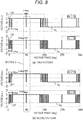
-
FIG. 8 illustrates the pulse pattern which is optimized with the loss coefficient λ = 0.5. These pulse patterns have the characteristics as follows. - (a) The optimized pulse pattern includes a pattern in which the pulse voltage Vu is turned on at the voltage phase θ* = 0 deg as illustrated in
FIG. 8(a) , and a pattern in which the pulse voltage Vu is turned off at the voltage phase θ* = 0 deg as illustrated inFIG. 8(b) . Hereinbelow, the former is called a first pattern, and the latter is called a second pattern. - (b) The optimal pulse pattern is turned off within ±0.6 deg from the voltage phase θ* = 90 deg as illustrated in the section A of
FIG. 8 . - (c) In the optimized pulse pattern, the pulse voltage Vu is turned on and off within ±22 deg from the voltage phase θ* = 0 deg.
- (d) At the voltage phase θ* other than (a) to (c), the pulse voltage Vu is kept on or off.
- The following restrictions are necessary in order to mount the optimized pulse pattern in the PWM control.
- (A) In the optimized pulse pattern, two or more control angles α are disposed in one period of the carrier wave Vc* as illustrated in
FIG. 9(a) , and are not symmetrically disposed with respect to the carrier wave Vc*. Therefore, as illustrated inFIG. 9(b) , two control angles α are disposed in one period of the carrier wave Vc*, and are necessarily disposed symmetrically with respect to the carrier wave Vc*. - (B) While under the restriction of (A), the pulse number Pn is not changed even when the modulation rate Kh* is increased.
- Hitherto, the description has been given about the optimization of the pulse pattern.
- In the embodiment, the synchronous correction signal A is generated using the
frequency correction unit 4, the correctionamount calculation unit 10, the synchronous correctionphase calculation unit 12, and the correctionsignal generation unit 13, and the pulse pattern holding the above characteristics (a) to (d) and the restrictions (A) and (B) is output to theinverter 2. Hereinbelow, the principle will be described. - With the characteristic (a), the carrier wave Vc* receives the restriction of (Mathematical Formula 8) in the case of the first pattern (the pattern P = 1), and receives the restriction of (Mathematical Formula 9) in the case of the second pattern (the pattern P = 2). In addition, with the characteristic (b), the carrier wave Vc* receives the restriction of (Mathematical Formula 10).
[Mathematical Formula 8]
[Mathematical Formula 9]
[Mathematical Formula 10]
- The
frequency correction unit 4 calculates the correction signal fc2* on the basis of the base number B and the pattern P so as to satisfy the restriction of (Mathematical Formula 8) or (Mathematical Formula 9), (Mathematical Formula 10), and (Mathematical Formula 1). - The pulse voltage Vu keeps (b) to (d) while satisfying the restrictions (A) and (B). In order to keep the characteristic, the zero holding phase β0 is calculated on the basis of (Mathematical Formula 11).
[Mathematical Formula 11]
- Herein, a correction base number B2 is a ratio of the corrected carrier frequency fc2* to the fundamental wave frequency f1*.
- In addition, the zero-cross phase β1 is calculated on the basis of (Mathematical Formula 12) or (Mathematical Formula 13) .
[Mathematical Formula 12]
[Mathematical Formula 13]
- The peak phase β2 is calculated by (Mathematical Formula 14) .
[Mathematical Formula 14]
- In a case where the modulation rate Kh* is larger than 1.22, the peak correction amount A1 is calculated by (Mathematical Formula 15) on the basis of the modulation rate Kh*. In a case where the modulation rate Kh* is smaller than 1.22, the peak correction amount A1 is calculated by (Mathematical Formula 16) on the basis of the control angle α without depending on the modulation rate Kh*. Herein, the control angle α is a value which is optimized to reduce or minimize the harmonic loss Wh on the basis of (Mathematical Formula 7).
[Mathematical Formula 15]
[Mathematical Formula 16]
- The synchronous correction signal A is generated to satisfy (Mathematical Formula 17).
[Mathematical Formula 17]
- The synchronous correction signal A when the voltage phase θ* is 90 - 360 (deg) is determined by the symmetry of the waveform.
-
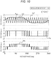
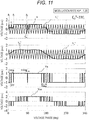
FIG. 10 illustrates a waveform diagram of the 3rd harmonic superimposed system in which the carrier frequency fc* = 1050 Hz, the fundamental wave frequency f1* = 50 Hz, the modulation rate Kh* = 1.2, the pulse number Pn per one period = 13, and the base number B = 21. The pulse pattern of the invention which is corrected on the basis of this pulse pattern is illustrated inFIG. 11 . The parameters of the pulse patterns after correction illustrated inFIG. 11 are as follows. - Corrected carrier frequency fc2* = 33 × f1*
- Peak correction amount Am = 0
- Zero-cross correction amount A1 = 0.1
- Pulse number Pn = 13
-
FIG. 12 illustrates the pulse pattern when the modulation rate Kh* of the pulse pattern illustrated inFIG. 11 is changed up to 1.15 - 1.21. These pulse patterns have the following characteristics. - In a range that the modulation rate Kh* falls within 1.15 - 1.21, the control angles α of the pulse voltage Vu near the voltage phase θ* = 0 deg are equal.
- In a range that the modulation rate Kh* falls within 1.15 - 1.21, the pulse voltage Vu near the voltage phase θ* = 0 deg is turned on and turned off within 24 deg. Herein, in all the pulse patterns designed in the first embodiment, the pulse voltage Vu near the voltage phase θ* = 0 deg is turned on and off within an electric angle of 38 deg.
- In a range that the modulation rate Kh* falls within 1.15 - 1.21, the pulse voltage Vu near the voltage phase θ* = 90 deg is turned off within 1.6 deg according to the change of the modulation rate Kh*. Herein, in all the pulse patterns designed in the first embodiment, the pulse voltage Vu near the voltage phase θ* = 90 deg is turned off within 5 deg.
- The pulse pattern in a case where the modulation rate Kh* is larger than 1.22 is illustrated in
FIG. 13 . In the embodiment, in a case where the modulation rate Kh* is larger than 1.22, the pulse voltage Vu near the voltage phase θ* = 90 deg is necessarily kept on. Therefore, the peak correction amount Am is set to "1." - The effect of the embodiment is illustrated in
FIG. 14 . Herein, the harmonic loss Wh is calculated as the loss coefficient λ = 0.5 on the basis of (Mathematical Formula 7) . In addition, when the harmonic number n is larger than "200," the harmonic loss is assumed as "0." As illustrated inFIG. 14 , the pulse pattern of the invention can reduce the harmonic loss Wh compared to the pulse pattern before correction, and the reduced amount is 43% at maximum. -
FIG. 15 is a diagram illustrating a configuration of a second embodiment, and FIG. 21 illustrates its components. However, the same components as those of the first embodiment will be omitted. - A carrier
wave generation unit 3 outputs the carrier wave Vc* on the basis of the carrier frequency fc*. An asynchronous correctionphase calculation unit 16 calculates a second zero holding phase β02, a second zero-cross phase β12, and a second peak phase β22 on the basis of the base number B and the pulse number Pn. - The correction
signal generation unit 13 generates an asynchronous correction signal A2 on the basis of the second zero holding phase β02, the second zero-cross phase β12, the second peak phase β22, the zero-cross correction amount A1, the peak correction amount Am, and the voltage phase θ*. - Hitherto, the description has been given about the configuration of the second embodiment. Next, the content of the second embodiment will be described.
- In the second embodiment, the harmonic loss of the over-modulation region in the asynchronous PWM control is reduced. In the asynchronous PWM control, the carrier frequency fc* is fixed regardless of the fundamental wave frequency f1*. Therefore, the zero-cross points at which the signs of the carrier wave Vc* and the signal wave Vu* are switched are not matched as illustrated in B of
FIG. 16 . In the asynchronous PWM control, the waveform of the pulse voltage Vu becomes an aperiodic waveform with respect to the period T1 of the signal since the zero-cross points of the signal wave Vu* and the carrier wave Vc* are not matched. However, as illustrated inFIG. 17 , the waveform becomes a periodic waveform with respect to a period T which is a least common multiple of the period T1 of the signal wave and a period Tc of the carrier wave. Therefore, in the second embodiment, the harmonic voltage Vn is obtained by (Mathematical Formula 18) with a least common period T as a reference.
[Mathematical Formula 18]
- Therefore, in the asynchronous PWM control, the harmonic component is generated even in a region lower than that of a fundamental component as illustrated in
FIG. 16(b) . The control angle α is calculated to reduce or minimize (Mathematical Formula 19) which is obtained by substituting (Mathematical Formula 18) into (Mathematical Formula 6). In addition, the modulation rate Kh* which is the constraint condition of (Mathematical Formula 19 is fixed to 1.2 in calculation.
[Mathematical Formula 19]
-
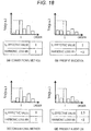
FIG. 18 illustrates the effect of the second embodiment. InFIGS. 18(a) and 18(b) , in the conventional method and the invention, the harmonic loss Wh can be reduced regardless of the fact that the effective values of the voltage harmonic Vn are equal. In addition, inFIGS. 18(c) and 18(d) , the harmonic loss Wh can be reduced regardless of the fact that the effective value of the voltage harmonic Vn is increased. -
FIG. 19 is a diagram illustrating a configuration of a third embodiment, in which the first or second embodiment is mounted in the drive system to drive the alternating-current motor 1. - In the third embodiment, a host device such as a
computer 17 outputs a torque command τ* or a frequency command f*. - A V/
f control unit 18 and avector control unit 19 calculate the fundamental wave frequency f1* and the modulation rate Kh* on the basis of the torque command τ* or the frequency command f*. - A control
mode changing unit 20 switches the torque command τ* and the frequency command f*. Acontrol selection unit 21 switches the V/f control unit 18 and thevector control unit 19. - A
phase calculation unit 22 calculates the voltage phase θ* on the basis of the fundamental wave frequency f1*. The fundamental wave frequency f1*, the voltage phase θ*, and the modulation rate Kh* calculated in the third embodiment are output to the motor control device of the first or second embodiment to drive the alternating-current motor 1. - According to the embodiment, the torque command τ* or the frequency command f*, and the
vector control unit 19 or the V/f control unit 18 may be set arbitrarily as an instruction value. -
- 1 alternating-current motor
- 2 inverter
- 3 frequency calculation unit
- 4 frequency correction unit
- 5 first modulation mode determination unit
- 6 carrier wave generation unit
- 7 amplitude calculation unit
- 8 second modulation mode determination unit
- 9 signal wave generation unit
- 10 correction amount calculation unit
- 10a control angle calculation unit
- 10b peak correction amount calculation unit
- 10c zero-cross corrected amount calculation unit
- 11 pattern determination unit
- 12 synchronous correction phase calculation unit
- 13 correction signal generation unit
- 14 third modulation mode determination unit
- 15 PWM control unit
- 16 asynchronous correction phase calculation unit
- 17 computer
- 18 V/f control unit
- 19 vector control unit
- 20 control mode switching unit
- 21 control selection unit
- 22 phase calculation unit
- VDC DC voltage
- Vu, Vv, Vw U-phase pulse voltage, V-phase pulse voltage, W-phase pulse voltage
- Iu, Iv, Iw U-phase current, V-phase current, W-phase current
- Vu*, Vv*, Vw* U-phase signal wave, V-phase signal wave, W-phase signal wave
- Vu2*, Vv2*, Vw2* U-phase correction signal wave, V-phase correction signal wave, W-phase correction signal wave
- Vuv line voltage
- Vc* carrier wave
- P pattern
- A synchronous correction signal
- A* final correction signal
- A1 zero-cross correction amount
- Am peak correction amount
- Vn harmonic voltage
- Guu, Gup U-phase gate signal
- Gvu, Gvp V-phase gate signal
- Gwu, Gwp W-phase gate signal
- θ* voltage phase
- f* frequency command
- τ* torque command
- Kh* modulation rate
- f1* fundamental wave frequency
- fc** final carrier wave frequency
- fc* carrier wave frequency
- fc2* corrected carrier wave frequency
- Tc carrier wave period
- T1 signal wave period
- T least common period of carrier wave and signal wave
- In harmonic current
- Z impedance of alternating-current motor
- L inductance of alternating-current motor
- λ loss coefficient
- n harmonic number
- Wh harmonic loss
- α control angle
- β0 zero holding phase
- β1 zero-cross phase
- β2 peak phase
- β02 second zero holding phase
- β12 second zero-cross phase
- β22 second peak phase
- Amp1 first amplitude
- Amp2 fixed amplitude
- Amp final amplitude
- fcmax maximum carrier frequency
- Pn pulse number
Claims (9)
- A motor control device including:an amplitude calculation unit which calculates a first amplitude on the basis of a modulation rate normalized by a DC voltage;a signal wave generation unit which generates a signal wave on the basis of a voltage phase and the first amplitude;a frequency calculation unit which calculates a base number and a carrier frequency on the basis of a fundamental wave frequency;a carrier wave generation unit which generates a carrier wave on the basis of the carrier frequency;a PWM control unit which compares the signal wave and the carrier wave, and outputs a gate signal; andan inverter which controls a switching element on the basis of the gate signal, and outputs a pulse voltage, the motor control device comprising:a frequency correction unit which calculates a corrected carrier frequency on the basis of the base number which is a ratio of the carrier frequency to the fundamental wave frequency, and a pattern;a pattern determination unit which calculates the pattern on the basis of the base number;a first modulation mode determination unit which switches a final carrier frequency from the carrier frequency to the corrected carrier frequency in a case where the modulation rate reaches a predetermined value equal to or greater than one;a correction amount calculation unit which calculates a pulse number, a zero-cross correction amount, and a peak correction amount on the basis of the modulation rate, the voltage phase, and the base number;a synchronous correction phase calculation unit which calculates a zero holding phase, a zero-cross phase, and a peak phase on the basis of the pulse number, the corrected carrier frequency, the pattern, and the fundamental wave frequency;a correction signal generation unit which generates a synchronous correction signal on the basis of the zero holding phase, the zero-cross phase, the peak phase, the peak correction amount, the zero-cross correction amount, and the voltage phase;a second modulation mode determination unit which switches a final correction signal wave from zero to the synchronous correction signal in a case where the modulation rate reaches a predetermined value equal to or greater than one; anda third modulation mode determination unit which switches a final amplitude from the first amplitude to a fixed amplitude in a case where the modulation rate reaches a predetermined value equal to or greater than one.
- The motor control device according to claim 1,
wherein the correction amount calculation unit is configured to include
a control angle calculation unit which calculates the pulse number and the control angle to reduce or minimize a harmonic loss of the following mathematical formula on the basis of the modulation rate and the base number,
a second pattern determination unit which determines the pattern on the basis of the base number,
a zero-cross correction amount calculation unit which calculates the zero-cross correction amount on the basis of the pulse number, the control angle, and the modulation rate, and
a peak correction amount calculation unit which calculates the peak amount correction unit on the basis of the modulation rate.
- The motor control device according to claim 1,
wherein the zero-cross correction phase is calculated to turn on and off the pulse voltage within ±38 deg from each of the voltage phases 0 and 180 deg, and
the peak correction phase is calculated to be turned off within ±5 deg from each of the voltage phases 90 and 270 deg. - The motor control device according to claim 1,
wherein, in a case where the modulation rate is smaller than 1.22, the zero-cross correction amount is calculated regardless of the modulation rate even when the modulation rate is changed, and
the zero-cross correction amount is calculated such that a timing of turning the pulse voltage on and off is matched in a region within ±38 deg from each of the voltage phases 0 and 180 deg. - The motor control device according to claim 1,
wherein, in a case where the modulation rate is smaller than 1.22, the peak correction amount is calculated such that the pulse voltage is turned off within ±5 deg from each of the voltage phases 90 and 270 deg on the basis of the modulation rate. - The motor control device according to claim 1,
wherein, in a case where the modulation rate is larger than 1.22, the zero-cross correction amount is calculated on the basis of the modulation rate, and
the peak correction amount is set to 1. - The motor control device according to claim 1, further comprising:in a case where the carrier wave is a fixed value regardless of the fundamental wave frequency,an asynchronous correction phase calculation unit 16 which calculates a second zero holding phase β02, a second zero-cross phase β12, and a second peak phase β22 on the basis of the base number and the pulse number Pn; anda correction signal generation unit which generates an asynchronous correction signal on the basis of the second zero holding phase, the second zero-cross phase, the second peak phase β22, the zero-cross correction amount A1, the peak correction amount Am, and a voltage phase θ*.
- The motor control device according to claim 7,
wherein the control angle is calculated to reduce or minimize the following mathematical formula with reference to a least common period of a period of the signal wave and a period of the carrier wave.
- A motor drive system, comprising:the motor control device according to any one of claims 1 to 8;a vector control unit and a V/f control unit which calculate the fundamental wave frequency and the modulation rate on the basis of a torque command or a frequency command;a control selection unit which switches the vector control unit and the V/f control unit;a control mode switching unit which switches the torque command and the frequency command; anda phase calculation unit which calculates the voltage phase on the basis of the fundamental wave frequency.
Applications Claiming Priority (2)
| Application Number | Priority Date | Filing Date | Title |
|---|---|---|---|
| JP2016050388A JP6674804B2 (en) | 2016-03-15 | 2016-03-15 | Motor control device and drive system |
| PCT/JP2017/003085 WO2017159072A1 (en) | 2016-03-15 | 2017-01-30 | Motor control device and drive system |
Publications (3)
| Publication Number | Publication Date |
|---|---|
| EP3432467A1 true EP3432467A1 (en) | 2019-01-23 |
| EP3432467A4 EP3432467A4 (en) | 2019-10-23 |
| EP3432467B1 EP3432467B1 (en) | 2022-04-06 |
Family
ID=59852256
Family Applications (1)
| Application Number | Title | Priority Date | Filing Date |
|---|---|---|---|
| EP17766080.0A Active EP3432467B1 (en) | 2016-03-15 | 2017-01-30 | Motor control device and drive system |
Country Status (4)
| Country | Link |
|---|---|
| EP (1) | EP3432467B1 (en) |
| JP (1) | JP6674804B2 (en) |
| CN (1) | CN108476011B (en) |
| WO (1) | WO2017159072A1 (en) |
Cited By (1)
| Publication number | Priority date | Publication date | Assignee | Title |
|---|---|---|---|---|
| US11674459B2 (en) | 2019-09-25 | 2023-06-13 | Honda Motor Co., Ltd. | Control apparatus, vehicle system, and control method |
Families Citing this family (2)
| Publication number | Priority date | Publication date | Assignee | Title |
|---|---|---|---|---|
| CN111585499B (en) * | 2019-02-18 | 2023-07-21 | 本田技研工业株式会社 | Control device, vehicle system, and control method |
| CN111342726B (en) * | 2020-03-26 | 2023-05-30 | 武汉科技大学 | Direct torque control method and system for permanent magnet synchronous motor |
Family Cites Families (7)
| Publication number | Priority date | Publication date | Assignee | Title |
|---|---|---|---|---|
| JP4417323B2 (en) * | 2005-11-18 | 2010-02-17 | 三菱電機株式会社 | Motor control device |
| JP4858597B2 (en) * | 2008-11-28 | 2012-01-18 | 株式会社デンソー | Rotating machine control device and manufacturing method thereof |
| JP4911241B1 (en) * | 2010-11-16 | 2012-04-04 | ダイキン工業株式会社 | Power converter |
| JP5873716B2 (en) * | 2011-12-28 | 2016-03-01 | 日立アプライアンス株式会社 | Motor control device |
| JP6078282B2 (en) * | 2012-09-28 | 2017-02-08 | 株式会社日立製作所 | AC motor drive system and motor vehicle |
| JP6204121B2 (en) * | 2013-09-09 | 2017-09-27 | 株式会社日立製作所 | Motor drive system and electric railway vehicle equipped with the system |
| JP6239448B2 (en) * | 2014-06-18 | 2017-11-29 | 株式会社日立製作所 | Inverter and drive system using the same |
-
2016
- 2016-03-15 JP JP2016050388A patent/JP6674804B2/en active Active
-
2017
- 2017-01-30 EP EP17766080.0A patent/EP3432467B1/en active Active
- 2017-01-30 CN CN201780007490.XA patent/CN108476011B/en not_active Expired - Fee Related
- 2017-01-30 WO PCT/JP2017/003085 patent/WO2017159072A1/en active Application Filing
Cited By (1)
| Publication number | Priority date | Publication date | Assignee | Title |
|---|---|---|---|---|
| US11674459B2 (en) | 2019-09-25 | 2023-06-13 | Honda Motor Co., Ltd. | Control apparatus, vehicle system, and control method |
Also Published As
| Publication number | Publication date |
|---|---|
| JP6674804B2 (en) | 2020-04-01 |
| JP2017169295A (en) | 2017-09-21 |
| WO2017159072A1 (en) | 2017-09-21 |
| EP3432467B1 (en) | 2022-04-06 |
| CN108476011B (en) | 2021-05-28 |
| CN108476011A (en) | 2018-08-31 |
| EP3432467A4 (en) | 2019-10-23 |
Similar Documents
| Publication | Publication Date | Title |
|---|---|---|
| US10153714B2 (en) | Adaptive pulse width modulation in motor control systems | |
| EP2611019B1 (en) | Control apparatus for regenerative medium voltage inverter | |
| EP3528383A1 (en) | Control device and control method for alternating current motor, and alternating current motor driving system | |
| EP3082247B1 (en) | Offset voltage generator and method for generating an offset voltage of three-phase inverter | |
| EP3509210B1 (en) | Inverter control device and electric motor driving system | |
| WO2015115223A1 (en) | Inverter control method and voltage-type inverter | |
| JP2008199709A (en) | Inverter controller, and ac motor controller | |
| EP3432467B1 (en) | Motor control device and drive system | |
| EP3482491B1 (en) | Closed loop flux weakening for permanent magent synchronous motors | |
| WO2017119214A1 (en) | Electric power converting device | |
| EP2692050B1 (en) | Common mode hysteresis for pulse-width modulation drives | |
| EP3276820B1 (en) | Motor control device | |
| EP2692045B1 (en) | Rate limited common mode control for pulse-width modulation drives | |
| EP2713501B1 (en) | A motor driving system and a motor vehicle | |
| JP2013179758A (en) | Electric power conversion device | |
| US11303224B2 (en) | Inverter device with high follow-up capability | |
| Hoang et al. | Online feedback-based field weakening control of interior permanent magnet brushless AC drives for traction applications accounting for nonlinear inverter characteristics | |
| Guerra et al. | Application of model predictive pulse pattern control to control a PMSM | |
| Nishizawa et al. | Reduction of dc-link current harmonics over wide power-factor range for three-phase VSI using single-carrier-comparison continuous PWM | |
| Son et al. | Hybrid mode control of an asymmetric dual three-phase synchronous motor under single-phase open fault | |
| US20230396200A1 (en) | Method for operating an electric motor | |
| EP3285386B1 (en) | Matrix direct ac/ac converter | |
| JP5399955B2 (en) | Power converter and control method of power converter | |
| JP2017022882A (en) | Power conversion device | |
| Styński et al. | Space Vector Modulation in Three-Phase Three-Level Flying Capacitor Converter-Fed Adjustable Speed Drive |
Legal Events
| Date | Code | Title | Description |
|---|---|---|---|
| STAA | Information on the status of an ep patent application or granted ep patent |
Free format text: STATUS: THE INTERNATIONAL PUBLICATION HAS BEEN MADE |
|
| PUAI | Public reference made under article 153(3) epc to a published international application that has entered the european phase |
Free format text: ORIGINAL CODE: 0009012 |
|
| STAA | Information on the status of an ep patent application or granted ep patent |
Free format text: STATUS: REQUEST FOR EXAMINATION WAS MADE |
|
| 17P | Request for examination filed |
Effective date: 20180824 |
|
| AK | Designated contracting states |
Kind code of ref document: A1 Designated state(s): AL AT BE BG CH CY CZ DE DK EE ES FI FR GB GR HR HU IE IS IT LI LT LU LV MC MK MT NL NO PL PT RO RS SE SI SK SM TR |
|
| AX | Request for extension of the european patent |
Extension state: BA ME |
|
| STAA | Information on the status of an ep patent application or granted ep patent |
Free format text: STATUS: REQUEST FOR EXAMINATION WAS MADE |
|
| DAV | Request for validation of the european patent (deleted) | ||
| DAX | Request for extension of the european patent (deleted) | ||
| A4 | Supplementary search report drawn up and despatched |
Effective date: 20190924 |
|
| RIC1 | Information provided on ipc code assigned before grant |
Ipc: H02P 27/08 20060101AFI20190918BHEP Ipc: H02P 21/00 20160101ALI20190918BHEP Ipc: H02P 27/04 20160101ALI20190918BHEP |
|
| GRAP | Despatch of communication of intention to grant a patent |
Free format text: ORIGINAL CODE: EPIDOSNIGR1 |
|
| STAA | Information on the status of an ep patent application or granted ep patent |
Free format text: STATUS: GRANT OF PATENT IS INTENDED |
|
| INTG | Intention to grant announced |
Effective date: 20211028 |
|
| GRAJ | Information related to disapproval of communication of intention to grant by the applicant or resumption of examination proceedings by the epo deleted |
Free format text: ORIGINAL CODE: EPIDOSDIGR1 |
|
| STAA | Information on the status of an ep patent application or granted ep patent |
Free format text: STATUS: REQUEST FOR EXAMINATION WAS MADE |
|
| GRAP | Despatch of communication of intention to grant a patent |
Free format text: ORIGINAL CODE: EPIDOSNIGR1 |
|
| STAA | Information on the status of an ep patent application or granted ep patent |
Free format text: STATUS: GRANT OF PATENT IS INTENDED |
|
| INTC | Intention to grant announced (deleted) | ||
| INTG | Intention to grant announced |
Effective date: 20220110 |
|
| GRAS | Grant fee paid |
Free format text: ORIGINAL CODE: EPIDOSNIGR3 |
|
| GRAA | (expected) grant |
Free format text: ORIGINAL CODE: 0009210 |
|
| STAA | Information on the status of an ep patent application or granted ep patent |
Free format text: STATUS: THE PATENT HAS BEEN GRANTED |
|
| AK | Designated contracting states |
Kind code of ref document: B1 Designated state(s): AL AT BE BG CH CY CZ DE DK EE ES FI FR GB GR HR HU IE IS IT LI LT LU LV MC MK MT NL NO PL PT RO RS SE SI SK SM TR |
|
| REG | Reference to a national code |
Ref country code: GB Ref legal event code: FG4D |
|
| REG | Reference to a national code |
Ref country code: CH Ref legal event code: EP |
|
| REG | Reference to a national code |
Ref country code: AT Ref legal event code: REF Ref document number: 1482329 Country of ref document: AT Kind code of ref document: T Effective date: 20220415 |
|
| REG | Reference to a national code |
Ref country code: DE Ref legal event code: R096 Ref document number: 602017055609 Country of ref document: DE |
|
| REG | Reference to a national code |
Ref country code: IE Ref legal event code: FG4D |
|
| REG | Reference to a national code |
Ref country code: LT Ref legal event code: MG9D |
|
| REG | Reference to a national code |
Ref country code: NL Ref legal event code: MP Effective date: 20220406 |
|
| REG | Reference to a national code |
Ref country code: AT Ref legal event code: MK05 Ref document number: 1482329 Country of ref document: AT Kind code of ref document: T Effective date: 20220406 |
|
| PG25 | Lapsed in a contracting state [announced via postgrant information from national office to epo] |
Ref country code: NL Free format text: LAPSE BECAUSE OF FAILURE TO SUBMIT A TRANSLATION OF THE DESCRIPTION OR TO PAY THE FEE WITHIN THE PRESCRIBED TIME-LIMIT Effective date: 20220406 |
|
| PG25 | Lapsed in a contracting state [announced via postgrant information from national office to epo] |
Ref country code: SE Free format text: LAPSE BECAUSE OF FAILURE TO SUBMIT A TRANSLATION OF THE DESCRIPTION OR TO PAY THE FEE WITHIN THE PRESCRIBED TIME-LIMIT Effective date: 20220406 Ref country code: PT Free format text: LAPSE BECAUSE OF FAILURE TO SUBMIT A TRANSLATION OF THE DESCRIPTION OR TO PAY THE FEE WITHIN THE PRESCRIBED TIME-LIMIT Effective date: 20220808 Ref country code: NO Free format text: LAPSE BECAUSE OF FAILURE TO SUBMIT A TRANSLATION OF THE DESCRIPTION OR TO PAY THE FEE WITHIN THE PRESCRIBED TIME-LIMIT Effective date: 20220706 Ref country code: LT Free format text: LAPSE BECAUSE OF FAILURE TO SUBMIT A TRANSLATION OF THE DESCRIPTION OR TO PAY THE FEE WITHIN THE PRESCRIBED TIME-LIMIT Effective date: 20220406 Ref country code: HR Free format text: LAPSE BECAUSE OF FAILURE TO SUBMIT A TRANSLATION OF THE DESCRIPTION OR TO PAY THE FEE WITHIN THE PRESCRIBED TIME-LIMIT Effective date: 20220406 Ref country code: GR Free format text: LAPSE BECAUSE OF FAILURE TO SUBMIT A TRANSLATION OF THE DESCRIPTION OR TO PAY THE FEE WITHIN THE PRESCRIBED TIME-LIMIT Effective date: 20220707 Ref country code: FI Free format text: LAPSE BECAUSE OF FAILURE TO SUBMIT A TRANSLATION OF THE DESCRIPTION OR TO PAY THE FEE WITHIN THE PRESCRIBED TIME-LIMIT Effective date: 20220406 Ref country code: ES Free format text: LAPSE BECAUSE OF FAILURE TO SUBMIT A TRANSLATION OF THE DESCRIPTION OR TO PAY THE FEE WITHIN THE PRESCRIBED TIME-LIMIT Effective date: 20220406 Ref country code: BG Free format text: LAPSE BECAUSE OF FAILURE TO SUBMIT A TRANSLATION OF THE DESCRIPTION OR TO PAY THE FEE WITHIN THE PRESCRIBED TIME-LIMIT Effective date: 20220706 Ref country code: AT Free format text: LAPSE BECAUSE OF FAILURE TO SUBMIT A TRANSLATION OF THE DESCRIPTION OR TO PAY THE FEE WITHIN THE PRESCRIBED TIME-LIMIT Effective date: 20220406 |
|
| PG25 | Lapsed in a contracting state [announced via postgrant information from national office to epo] |
Ref country code: RS Free format text: LAPSE BECAUSE OF FAILURE TO SUBMIT A TRANSLATION OF THE DESCRIPTION OR TO PAY THE FEE WITHIN THE PRESCRIBED TIME-LIMIT Effective date: 20220406 Ref country code: PL Free format text: LAPSE BECAUSE OF FAILURE TO SUBMIT A TRANSLATION OF THE DESCRIPTION OR TO PAY THE FEE WITHIN THE PRESCRIBED TIME-LIMIT Effective date: 20220406 Ref country code: LV Free format text: LAPSE BECAUSE OF FAILURE TO SUBMIT A TRANSLATION OF THE DESCRIPTION OR TO PAY THE FEE WITHIN THE PRESCRIBED TIME-LIMIT Effective date: 20220406 Ref country code: IS Free format text: LAPSE BECAUSE OF FAILURE TO SUBMIT A TRANSLATION OF THE DESCRIPTION OR TO PAY THE FEE WITHIN THE PRESCRIBED TIME-LIMIT Effective date: 20220806 |
|
| REG | Reference to a national code |
Ref country code: DE Ref legal event code: R097 Ref document number: 602017055609 Country of ref document: DE |
|
| PG25 | Lapsed in a contracting state [announced via postgrant information from national office to epo] |
Ref country code: SM Free format text: LAPSE BECAUSE OF FAILURE TO SUBMIT A TRANSLATION OF THE DESCRIPTION OR TO PAY THE FEE WITHIN THE PRESCRIBED TIME-LIMIT Effective date: 20220406 Ref country code: SK Free format text: LAPSE BECAUSE OF FAILURE TO SUBMIT A TRANSLATION OF THE DESCRIPTION OR TO PAY THE FEE WITHIN THE PRESCRIBED TIME-LIMIT Effective date: 20220406 Ref country code: RO Free format text: LAPSE BECAUSE OF FAILURE TO SUBMIT A TRANSLATION OF THE DESCRIPTION OR TO PAY THE FEE WITHIN THE PRESCRIBED TIME-LIMIT Effective date: 20220406 Ref country code: EE Free format text: LAPSE BECAUSE OF FAILURE TO SUBMIT A TRANSLATION OF THE DESCRIPTION OR TO PAY THE FEE WITHIN THE PRESCRIBED TIME-LIMIT Effective date: 20220406 Ref country code: DK Free format text: LAPSE BECAUSE OF FAILURE TO SUBMIT A TRANSLATION OF THE DESCRIPTION OR TO PAY THE FEE WITHIN THE PRESCRIBED TIME-LIMIT Effective date: 20220406 Ref country code: CZ Free format text: LAPSE BECAUSE OF FAILURE TO SUBMIT A TRANSLATION OF THE DESCRIPTION OR TO PAY THE FEE WITHIN THE PRESCRIBED TIME-LIMIT Effective date: 20220406 |
|
| PLBE | No opposition filed within time limit |
Free format text: ORIGINAL CODE: 0009261 |
|
| STAA | Information on the status of an ep patent application or granted ep patent |
Free format text: STATUS: NO OPPOSITION FILED WITHIN TIME LIMIT |
|
| 26N | No opposition filed |
Effective date: 20230110 |
|
| PG25 | Lapsed in a contracting state [announced via postgrant information from national office to epo] |
Ref country code: AL Free format text: LAPSE BECAUSE OF FAILURE TO SUBMIT A TRANSLATION OF THE DESCRIPTION OR TO PAY THE FEE WITHIN THE PRESCRIBED TIME-LIMIT Effective date: 20220406 |
|
| PG25 | Lapsed in a contracting state [announced via postgrant information from national office to epo] |
Ref country code: SI Free format text: LAPSE BECAUSE OF FAILURE TO SUBMIT A TRANSLATION OF THE DESCRIPTION OR TO PAY THE FEE WITHIN THE PRESCRIBED TIME-LIMIT Effective date: 20220406 |
|
| PGFP | Annual fee paid to national office [announced via postgrant information from national office to epo] |
Ref country code: IT Payment date: 20221213 Year of fee payment: 7 |
|
| REG | Reference to a national code |
Ref country code: CH Ref legal event code: PL |
|
| GBPC | Gb: european patent ceased through non-payment of renewal fee |
Effective date: 20230130 |
|
| PG25 | Lapsed in a contracting state [announced via postgrant information from national office to epo] |
Ref country code: LU Free format text: LAPSE BECAUSE OF NON-PAYMENT OF DUE FEES Effective date: 20230130 |
|
| REG | Reference to a national code |
Ref country code: BE Ref legal event code: MM Effective date: 20230131 |
|
| PG25 | Lapsed in a contracting state [announced via postgrant information from national office to epo] |
Ref country code: LI Free format text: LAPSE BECAUSE OF NON-PAYMENT OF DUE FEES Effective date: 20230131 Ref country code: GB Free format text: LAPSE BECAUSE OF NON-PAYMENT OF DUE FEES Effective date: 20230130 Ref country code: CH Free format text: LAPSE BECAUSE OF NON-PAYMENT OF DUE FEES Effective date: 20230131 |
|
| PG25 | Lapsed in a contracting state [announced via postgrant information from national office to epo] |
Ref country code: BE Free format text: LAPSE BECAUSE OF NON-PAYMENT OF DUE FEES Effective date: 20230131 |
|
| PG25 | Lapsed in a contracting state [announced via postgrant information from national office to epo] |
Ref country code: IE Free format text: LAPSE BECAUSE OF NON-PAYMENT OF DUE FEES Effective date: 20230130 |
|
| PGFP | Annual fee paid to national office [announced via postgrant information from national office to epo] |
Ref country code: FR Payment date: 20231212 Year of fee payment: 8 |
|
| PGFP | Annual fee paid to national office [announced via postgrant information from national office to epo] |
Ref country code: DE Payment date: 20231205 Year of fee payment: 8 |