EP3082247B1 - Offset voltage generator and method for generating an offset voltage of three-phase inverter - Google Patents
Offset voltage generator and method for generating an offset voltage of three-phase inverter Download PDFInfo
- Publication number
- EP3082247B1 EP3082247B1 EP16160443.4A EP16160443A EP3082247B1 EP 3082247 B1 EP3082247 B1 EP 3082247B1 EP 16160443 A EP16160443 A EP 16160443A EP 3082247 B1 EP3082247 B1 EP 3082247B1
- Authority
- EP
- European Patent Office
- Prior art keywords
- voltage signal
- phase
- voltage
- limit value
- offset voltage
- Prior art date
- Legal status (The legal status is an assumption and is not a legal conclusion. Google has not performed a legal analysis and makes no representation as to the accuracy of the status listed.)
- Not-in-force
Links
Images


Classifications
-
- H—ELECTRICITY
- H02—GENERATION; CONVERSION OR DISTRIBUTION OF ELECTRIC POWER
- H02M—APPARATUS FOR CONVERSION BETWEEN AC AND AC, BETWEEN AC AND DC, OR BETWEEN DC AND DC, AND FOR USE WITH MAINS OR SIMILAR POWER SUPPLY SYSTEMS; CONVERSION OF DC OR AC INPUT POWER INTO SURGE OUTPUT POWER; CONTROL OR REGULATION THEREOF
- H02M7/00—Conversion of ac power input into dc power output; Conversion of dc power input into ac power output
- H02M7/42—Conversion of dc power input into ac power output without possibility of reversal
- H02M7/44—Conversion of dc power input into ac power output without possibility of reversal by static converters
- H02M7/48—Conversion of dc power input into ac power output without possibility of reversal by static converters using discharge tubes with control electrode or semiconductor devices with control electrode
-
- H—ELECTRICITY
- H02—GENERATION; CONVERSION OR DISTRIBUTION OF ELECTRIC POWER
- H02M—APPARATUS FOR CONVERSION BETWEEN AC AND AC, BETWEEN AC AND DC, OR BETWEEN DC AND DC, AND FOR USE WITH MAINS OR SIMILAR POWER SUPPLY SYSTEMS; CONVERSION OF DC OR AC INPUT POWER INTO SURGE OUTPUT POWER; CONTROL OR REGULATION THEREOF
- H02M1/00—Details of apparatus for conversion
- H02M1/12—Arrangements for reducing harmonics from ac input or output
-
- H—ELECTRICITY
- H02—GENERATION; CONVERSION OR DISTRIBUTION OF ELECTRIC POWER
- H02M—APPARATUS FOR CONVERSION BETWEEN AC AND AC, BETWEEN AC AND DC, OR BETWEEN DC AND DC, AND FOR USE WITH MAINS OR SIMILAR POWER SUPPLY SYSTEMS; CONVERSION OF DC OR AC INPUT POWER INTO SURGE OUTPUT POWER; CONTROL OR REGULATION THEREOF
- H02M7/00—Conversion of ac power input into dc power output; Conversion of dc power input into ac power output
- H02M7/42—Conversion of dc power input into ac power output without possibility of reversal
- H02M7/44—Conversion of dc power input into ac power output without possibility of reversal by static converters
- H02M7/48—Conversion of dc power input into ac power output without possibility of reversal by static converters using discharge tubes with control electrode or semiconductor devices with control electrode
- H02M7/53—Conversion of dc power input into ac power output without possibility of reversal by static converters using discharge tubes with control electrode or semiconductor devices with control electrode using devices of a triode or transistor type requiring continuous application of a control signal
- H02M7/537—Conversion of dc power input into ac power output without possibility of reversal by static converters using discharge tubes with control electrode or semiconductor devices with control electrode using devices of a triode or transistor type requiring continuous application of a control signal using semiconductor devices only, e.g. single switched pulse inverters
- H02M7/5387—Conversion of dc power input into ac power output without possibility of reversal by static converters using discharge tubes with control electrode or semiconductor devices with control electrode using devices of a triode or transistor type requiring continuous application of a control signal using semiconductor devices only, e.g. single switched pulse inverters in a bridge configuration
- H02M7/53871—Conversion of dc power input into ac power output without possibility of reversal by static converters using discharge tubes with control electrode or semiconductor devices with control electrode using devices of a triode or transistor type requiring continuous application of a control signal using semiconductor devices only, e.g. single switched pulse inverters in a bridge configuration with automatic control of output voltage or current
- H02M7/53873—Conversion of dc power input into ac power output without possibility of reversal by static converters using discharge tubes with control electrode or semiconductor devices with control electrode using devices of a triode or transistor type requiring continuous application of a control signal using semiconductor devices only, e.g. single switched pulse inverters in a bridge configuration with automatic control of output voltage or current with digital control
-
- H—ELECTRICITY
- H02—GENERATION; CONVERSION OR DISTRIBUTION OF ELECTRIC POWER
- H02P—CONTROL OR REGULATION OF ELECTRIC MOTORS, ELECTRIC GENERATORS OR DYNAMO-ELECTRIC CONVERTERS; CONTROLLING TRANSFORMERS, REACTORS OR CHOKE COILS
- H02P27/00—Arrangements or methods for the control of AC motors characterised by the kind of supply voltage
- H02P27/04—Arrangements or methods for the control of AC motors characterised by the kind of supply voltage using variable-frequency supply voltage, e.g. inverter or converter supply voltage
- H02P27/06—Arrangements or methods for the control of AC motors characterised by the kind of supply voltage using variable-frequency supply voltage, e.g. inverter or converter supply voltage using dc to ac converters or inverters
- H02P27/08—Arrangements or methods for the control of AC motors characterised by the kind of supply voltage using variable-frequency supply voltage, e.g. inverter or converter supply voltage using dc to ac converters or inverters with pulse width modulation
- H02P27/085—Arrangements or methods for the control of AC motors characterised by the kind of supply voltage using variable-frequency supply voltage, e.g. inverter or converter supply voltage using dc to ac converters or inverters with pulse width modulation wherein the PWM mode is adapted on the running conditions of the motor, e.g. the switching frequency
-
- H—ELECTRICITY
- H02—GENERATION; CONVERSION OR DISTRIBUTION OF ELECTRIC POWER
- H02M—APPARATUS FOR CONVERSION BETWEEN AC AND AC, BETWEEN AC AND DC, OR BETWEEN DC AND DC, AND FOR USE WITH MAINS OR SIMILAR POWER SUPPLY SYSTEMS; CONVERSION OF DC OR AC INPUT POWER INTO SURGE OUTPUT POWER; CONTROL OR REGULATION THEREOF
- H02M1/00—Details of apparatus for conversion
- H02M1/0003—Details of control, feedback or regulation circuits
- H02M1/0025—Arrangements for modifying reference values, feedback values or error values in the control loop of a converter
-
- H—ELECTRICITY
- H02—GENERATION; CONVERSION OR DISTRIBUTION OF ELECTRIC POWER
- H02M—APPARATUS FOR CONVERSION BETWEEN AC AND AC, BETWEEN AC AND DC, OR BETWEEN DC AND DC, AND FOR USE WITH MAINS OR SIMILAR POWER SUPPLY SYSTEMS; CONVERSION OF DC OR AC INPUT POWER INTO SURGE OUTPUT POWER; CONTROL OR REGULATION THEREOF
- H02M1/00—Details of apparatus for conversion
- H02M1/0048—Circuits or arrangements for reducing losses
- H02M1/0054—Transistor switching losses
-
- H—ELECTRICITY
- H02—GENERATION; CONVERSION OR DISTRIBUTION OF ELECTRIC POWER
- H02M—APPARATUS FOR CONVERSION BETWEEN AC AND AC, BETWEEN AC AND DC, OR BETWEEN DC AND DC, AND FOR USE WITH MAINS OR SIMILAR POWER SUPPLY SYSTEMS; CONVERSION OF DC OR AC INPUT POWER INTO SURGE OUTPUT POWER; CONTROL OR REGULATION THEREOF
- H02M7/00—Conversion of ac power input into dc power output; Conversion of dc power input into ac power output
- H02M7/42—Conversion of dc power input into ac power output without possibility of reversal
- H02M7/44—Conversion of dc power input into ac power output without possibility of reversal by static converters
- H02M7/48—Conversion of dc power input into ac power output without possibility of reversal by static converters using discharge tubes with control electrode or semiconductor devices with control electrode
- H02M7/483—Converters with outputs that each can have more than two voltages levels
-
- H—ELECTRICITY
- H02—GENERATION; CONVERSION OR DISTRIBUTION OF ELECTRIC POWER
- H02M—APPARATUS FOR CONVERSION BETWEEN AC AND AC, BETWEEN AC AND DC, OR BETWEEN DC AND DC, AND FOR USE WITH MAINS OR SIMILAR POWER SUPPLY SYSTEMS; CONVERSION OF DC OR AC INPUT POWER INTO SURGE OUTPUT POWER; CONTROL OR REGULATION THEREOF
- H02M7/00—Conversion of ac power input into dc power output; Conversion of dc power input into ac power output
- H02M7/42—Conversion of dc power input into ac power output without possibility of reversal
- H02M7/44—Conversion of dc power input into ac power output without possibility of reversal by static converters
- H02M7/48—Conversion of dc power input into ac power output without possibility of reversal by static converters using discharge tubes with control electrode or semiconductor devices with control electrode
- H02M7/497—Conversion of dc power input into ac power output without possibility of reversal by static converters using discharge tubes with control electrode or semiconductor devices with control electrode sinusoidal output voltages being obtained by combination of several voltages being out of phase
-
- H—ELECTRICITY
- H02—GENERATION; CONVERSION OR DISTRIBUTION OF ELECTRIC POWER
- H02M—APPARATUS FOR CONVERSION BETWEEN AC AND AC, BETWEEN AC AND DC, OR BETWEEN DC AND DC, AND FOR USE WITH MAINS OR SIMILAR POWER SUPPLY SYSTEMS; CONVERSION OF DC OR AC INPUT POWER INTO SURGE OUTPUT POWER; CONTROL OR REGULATION THEREOF
- H02M7/00—Conversion of ac power input into dc power output; Conversion of dc power input into ac power output
- H02M7/42—Conversion of dc power input into ac power output without possibility of reversal
- H02M7/44—Conversion of dc power input into ac power output without possibility of reversal by static converters
- H02M7/48—Conversion of dc power input into ac power output without possibility of reversal by static converters using discharge tubes with control electrode or semiconductor devices with control electrode
- H02M7/53—Conversion of dc power input into ac power output without possibility of reversal by static converters using discharge tubes with control electrode or semiconductor devices with control electrode using devices of a triode or transistor type requiring continuous application of a control signal
- H02M7/537—Conversion of dc power input into ac power output without possibility of reversal by static converters using discharge tubes with control electrode or semiconductor devices with control electrode using devices of a triode or transistor type requiring continuous application of a control signal using semiconductor devices only, e.g. single switched pulse inverters
- H02M7/5387—Conversion of dc power input into ac power output without possibility of reversal by static converters using discharge tubes with control electrode or semiconductor devices with control electrode using devices of a triode or transistor type requiring continuous application of a control signal using semiconductor devices only, e.g. single switched pulse inverters in a bridge configuration
- H02M7/53871—Conversion of dc power input into ac power output without possibility of reversal by static converters using discharge tubes with control electrode or semiconductor devices with control electrode using devices of a triode or transistor type requiring continuous application of a control signal using semiconductor devices only, e.g. single switched pulse inverters in a bridge configuration with automatic control of output voltage or current
- H02M7/53875—Conversion of dc power input into ac power output without possibility of reversal by static converters using discharge tubes with control electrode or semiconductor devices with control electrode using devices of a triode or transistor type requiring continuous application of a control signal using semiconductor devices only, e.g. single switched pulse inverters in a bridge configuration with automatic control of output voltage or current with analogue control of three-phase output
- H02M7/53876—Conversion of dc power input into ac power output without possibility of reversal by static converters using discharge tubes with control electrode or semiconductor devices with control electrode using devices of a triode or transistor type requiring continuous application of a control signal using semiconductor devices only, e.g. single switched pulse inverters in a bridge configuration with automatic control of output voltage or current with analogue control of three-phase output based on synthesising a desired voltage vector via the selection of appropriate fundamental voltage vectors, and corresponding dwelling times
-
- H—ELECTRICITY
- H02—GENERATION; CONVERSION OR DISTRIBUTION OF ELECTRIC POWER
- H02P—CONTROL OR REGULATION OF ELECTRIC MOTORS, ELECTRIC GENERATORS OR DYNAMO-ELECTRIC CONVERTERS; CONTROLLING TRANSFORMERS, REACTORS OR CHOKE COILS
- H02P2209/00—Indexing scheme relating to controlling arrangements characterised by the waveform of the supplied voltage or current
- H02P2209/13—Different type of waveforms depending on the mode of operation
-
- Y—GENERAL TAGGING OF NEW TECHNOLOGICAL DEVELOPMENTS; GENERAL TAGGING OF CROSS-SECTIONAL TECHNOLOGIES SPANNING OVER SEVERAL SECTIONS OF THE IPC; TECHNICAL SUBJECTS COVERED BY FORMER USPC CROSS-REFERENCE ART COLLECTIONS [XRACs] AND DIGESTS
- Y02—TECHNOLOGIES OR APPLICATIONS FOR MITIGATION OR ADAPTATION AGAINST CLIMATE CHANGE
- Y02B—CLIMATE CHANGE MITIGATION TECHNOLOGIES RELATED TO BUILDINGS, e.g. HOUSING, HOUSE APPLIANCES OR RELATED END-USER APPLICATIONS
- Y02B70/00—Technologies for an efficient end-user side electric power management and consumption
- Y02B70/10—Technologies improving the efficiency by using switched-mode power supplies [SMPS], i.e. efficient power electronics conversion e.g. power factor correction or reduction of losses in power supplies or efficient standby modes
Definitions
- the present disclosure relates to an offset voltage generator and a method for generating an offset voltage for controlling continuous modulation and discontinuous modulation of a three-phase inverter.
- US2012/249043 A1 discloses a prior art controller and inverter used to control a voltage level and frequency of signals that are used to drive a three phase electric motor.
- VVVF variable voltage and variable frequency
- PWM pulse width modulation
- the PWM scheme may be divided into continuous modulation scheme and discontinuous modulation scheme.
- Examples of the continuous modulation mode may include sinusoidal PWM (SPWM), space vector PWM (SVPWM), etc.
- Examples of the discontinuous modulation mode may include 60° discontinuous PWM (DPWM) for reducing switching loss of a power semiconductor.
- an offset voltage is compared to a carrier wave such as a triangular wave to modulate voltage. In doing so, different offset voltages are used in the continuous and discontinuous modulation modes.
- a carrier wave such as a triangular wave to modulate voltage.
- different offset voltages are used in the continuous and discontinuous modulation modes.
- MI modulation index
- TDD total harmonic distortion
- an offset voltage generator includes: a first limiter configured to compare a first phase-voltage signal with a maximum limit value and a minimum limit value to output a first limit-voltage signal; a second limiter configured to compare a second phase-voltage signal with the maximum limit value and the minimum limit value to output a second limit-voltage signal; a third limiter configured to compare a third phase-voltage signal with the maximum limit value and the minimum limit value to output a third limit-voltage signal; and a summer configured to add a difference between the first phase-voltage signal and the first limit-voltage signal, a difference between the second phase-voltage signal and the second limit-voltage signal, and a difference between the third phase-voltage signal and the third limit-voltage signal, to output an offset voltage.
- the maximum limit value and the minimum limit value are determined by a DC link voltage of the three-phase inverter.
- the summer outputs a different offset voltage depending on a modulation index determined by the DC link voltage of the three-phase inverter to switch between the continuous modulation mode and the discontinuous modulation mode of the three-phase inverter without additionally calculating another offset voltage.
- the voltage modulation mode of a three-phase inverter can be easily switched from the continuous modulation mode to the discontinuous modulation mode without any additional calculating process.
- a discontinuous modulation period is adjusted, such total harmonic distortion (THD) can be reduced in a period where the modulation index is low compared to the discontinuous modulation scheme in the related art, and switching loss can be reduced in a period where the modulation index is high compared to the continuous modulation scheme in the related art.
- TDD total harmonic distortion
- an offset voltage having the minimum RMS is generated, such that unnecessary zero sequence voltage can be reduced.
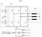
- FIG. 1 shows an example of a three-phase inverter to which a method for generating an offset voltage of a three-phase inverter according to an exemplary embodiment of the present disclosure is applied.
- the three-phase inverter shown in FIG. 1 is a typical two-level three-phase voltage source inverter used in driving an ESS or motor drive.
- the three-phase inverter includes a smoothing part 101 and a switching part 102.
- the three-phase inverter rectifies a three-phase AC voltage from an external device to a DC voltage by a rectifier (not shown).
- the rectified DC voltage is smoothed via the smoothing part 101 shown in FIG. 1 to DC link voltages of V dc /2 at two DC links.
- the symbol n in FIG. 1 represents a virtual DC link neutral point.
- the smoothed DC link voltages V dc /2 are converted to a three-phase AC voltage via a number of switching elements a1, a2, b1, b2, c1 and c2 in the switching part 102.
- the switching element a1 and the switching element a2 are turned on/off in a complementary fashion.
- the switching element b1 and the switching element b2 are turned on/off in a complementary fashion, and the switching element c1 and the switching element c2 are turned on/off in a complementary fashion.
- the three-phase AC voltage generated via the switching operations of the switching unit 102 is input to a load 103 such as an electric motor.
- the switching elements a1, a2, b1, b2, c1 and c2 in the switching part 102 are turned on/off in a complementary fashion, respectively, to generate a three-phase AC voltage.
- the switching operations (on/off operations) of the switching elements a1, a2, b1, b2, c1 and c2 are performed in accordance with control signals output from a PWM control unit 104 as shown in FIG. 1 .
- the PWM control unit 104 generates control signal for controlling the switching operations of the switching elements a1, a2, b1, b2, c1 and c2 using a three-phase voltage signal input from an external device.
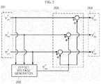
- FIG. 2 shows a process of generating a three-phase pole voltage signal by a pole voltage signal generator in the PWM control unit 104 in the related art.
- the pole-voltage signal generator in the PWM control unit 104 adds three phase-voltage signals 201 including a first phase-voltage signal V* as , a second phase-voltage signal V* bs and a third phase-voltage signal V* cs to an offset voltage V* sn generated in an offset voltage generator 202, respectively, thereby generating three-phase pole-voltage signals 203 including a first pole-voltage signal V* an , a second pole-voltage signal V* bn and a third pole-voltage signal V* cn .
- the offset voltage V* sn is a component that commonly exists in the pole-voltage signals 203, and is a zero sequence voltage such that it does not affect the combination of phase-to-phase voltages.
- FIG. 3 shows a process that a control signal generator in the PWM control unit 104 generates a control signal for switching elements by using three-phase pole-voltage signals in the related art.
- the pole-voltage signals 301 generated via the process of FIG. 2 i.e., the first pole-voltage signal V* an , the second pole-voltage signal V* bn and the third pole-voltage signal V* cn are compared with a carrier wave 302 as shown in FIG. 3 .
- the carrier wave 302 shown in FIG. 3 is a triangular carrier wave, other types of carrier waves may also be used depending on the modulation scheme.
- the frequency of the carrier wave 302 is equal to the switching frequency.
- the peak has the maximum value of V dc /2 and the minimum value of -V dc /2.
- the difference between each of the pole-voltage signals 201 and the carrier wave 302 is calculated, and the value of 1 is output if the difference is equal to or greater than 0, and the value of 0 is output if the difference is less than 0 (as indicated by reference numeral 303). Accordingly, an on-signal is output to the switching elements a1, b1 and c1 if the difference between each of the pole-voltage signals 201 and the carrier wave 302 is greater than 0, and an on-signal is output to the switching elements a2, b2 and c2 if the difference between each of the pole-voltage signals 201 and the carrier wave 302 is less than 0 by NOT gates 304.
- the modulation mode is finally determined based on the offset voltage V* sn generated in the offset voltage generator 202.
- the space vector PWM (SVPWM) expressed in Equation 3 is a continuous modulation scheme in which control signals for all of the switching elements are changed for a cycle of a carrier wave.
- a control signal for a switching element in a phase does not change, in order to reduce switching loss.
- One of the most commonly used discontinuous voltage modulation scheme is 60° discontinuous PWM (DPWM), in which switching discontinuous periods of 60° exist around the peak of a phase-voltage signal.
- the discontinuous modulation interval is always set to 120° of a cycle of a reference wave. Accordingly, when the modulation index MI is low, the THD in the output current is very large in the discontinuous modulation mode. As a result, there is another problem in the modulation index by which discontinuous modulation starts is restricted in order to reduce switching loss.
- the offset voltage is continuously generated even in a period where the offset voltage is not necessary and introduced into the inverter via the PWM control unit 104.
- the offset voltage is zero sequence voltage and may result in reduction in the power efficiency or malfunction of a load connected to the inverter. For example, if such zero sequence voltage is applied to an ESS using a grid connected inverter or a photovoltaic module, leakage current may be generated such that power efficiency may be reduced.
- leakage current may be generated such that power efficiency may be reduced.
- torque in the axial direction or bearing current becomes large, possibly causing dielectric breakdown.
- an offset voltage generator and a method for generating an offset voltage of a three-phase inverter that allow voltage modulation mode of the three-phase inverter to switch from a continuous modulation mode to a discontinuous modulation mode without additionally calculating another offset voltage.
- an offset voltage having the minimum RMS is generated to be introduced into the inverter and thus the zero sequence voltage is minimized, thereby preventing reduction in power efficiency and malfunction of a load driven by the inverter.
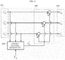
- FIG. 4 is a block diagram of a pole-voltage signal generator included in a PWM control unit 104 according to an exemplary embodiment of the present disclosure.
- the pole-voltage signal generator adds three phase-voltage signals 401 including a first phase-voltage signal V* as , a second phase-voltage signal V* bs and a third phase-voltage signal V* cs to an offset voltage V* sn generated in an offset voltage generator 402, respectively, (as indicated by reference numeral 403), thereby generating three-phase pole-voltage signals 404 including a first pole-voltage signal V* an , a second pole-voltage signal V* bn and a third pole-voltage signal V* cn .
- the offset voltage generator 402 according to the exemplary embodiment of the present disclosure generates an offset voltage V* sn by using phase-voltage signals 401 and a DC link voltage V dc of the three-phase inverter.
- the offset voltage V* sn of the inverter of FIG. 1 has the range as expressed in Equation 5 below: ⁇ V dc 2 ⁇ v min ⁇ v sn * ⁇ V dc 2 ⁇ v max
- V dc 2 ⁇ v max in Equation 5 ⁇ V dc 2 ⁇ v min ⁇ v sn * ⁇ V dc 2 ⁇ v max ⁇ 0 is established. That is, the offset voltage having the minimum absolute value becomes V dc 2 ⁇ v max .
- ⁇ V dc 2 > v min 0 ⁇ ⁇ V dc 2 ⁇ v min ⁇ v sn * ⁇ V dc 2 ⁇ v max is established, such that the offset voltage having the minimum absolute value becomes ⁇ V dc 2 ⁇ v min .
- FIG. 5 is block diagram of the offset voltage generator 402 according to an exemplary embodiment of the present disclosure.
- the offset voltage generator 402 generates the offset voltage V* sn as expressed in Equation 7 in the following manner.
- the offset voltage generator 402 according to the exemplary embodiment of the present disclosure includes a first limiter 502(a), a second limiter 502(b) and a third limiter 502(c) respectively corresponding to the first phase-voltage signal V* as , the second phase-voltage signal V* bs and the third phase-voltage signal V* cs .
- the first limiter 502(a) receives the first phase-voltage signal V* as and compares the received first phase-voltage signal V* as with the maximum limit value and the minimum limit value to output the first limit signal Vas.
- the maximum limit value may be set to V dc 2
- the minimum limit value may be set to ⁇ V dc 2 .
- the first limiter 502(a) outputs the first phase voltage signal V* as as the first limit signal Vas if the first phase voltage signal V* as is equal to or greater than the minimum limit value and equal to or less than the maximum limit value. In addition, the first limiter 502(a) outputs the minimum limit value as the first limit signal Vas if the first phase voltage signal V* as is less than the minimum limit value. In addition, the first limiter 502(a) outputs the maximum limit value as the first limit signal Vas if the first phase voltage signal V* as is greater than the maximum limit value.
- the second limiter 502(b) and the third limiter 502(c) also output the second limit signal Vbs and the third limit signal Vcs, respectively, in the same manner as the first limiter 502(a) described above.
- the 402 outputs, as the offset voltage V* sn , the sum of the difference between the first limit signal Vas and the first phase voltage signal V* as , the difference between the second limit signal Vbs and the second phase voltage signal V* bs , and the difference between the third limit signal Vcs and the third phase voltage signal V* cs , as shown in FIG. 5 .
- the offset voltage V* sn generated by the offset voltage generator 402 becomes 0 if the three phase-voltage signals 501 are between the minimum limit value and the maximum limit value.
- the PWM control unit 104 of FIG. 1 operates in the SPWM mode that is a continuous modulation scheme.
- the pole-voltage signal becomes V dc /2 or -V dc /2, such that the PWM control unit 104 is switched to the discontinuous modulation mode.
- the discontinuous operation range in which the PWM control unit 104 operates in the discontinuous modulation mode is determined by the modulation index MI.
- the voltage modulation mode of the three-phase inverter can be easily switched from the continuous modulation mode to the discontinuous modulation mode without any additional calculating process.
- a discontinuous modulation period is adjusted, such that total harmonic distortion (THD) can be reduced in a period where the modulation index is low compared to the discontinuous modulation scheme in the related art, and switching loss can be reduced in a period where the modulation index is high compared to the continuous modulation scheme in the related art.
- TDD total harmonic distortion
- FIGS. 6 to 8 are graphs for comparing waveforms of offset voltages and pole-voltages according to the PWM control scheme of the present disclosure, the SPWM control scheme in the related art, the SVPWM control scheme in the related art and the 60°DPWM in the related art with one another by varying the modulation index MI.
- the modulation index MI of the PWM control scheme according to the exemplary embodiment of the present disclosure is set to 1.
- FIG. 6 shows a waveform 601(a) of a pole-voltage signal according to the PWM control scheme according to the exemplary embodiment of the present disclosure and the SPWM control scheme in the related art, a waveform 602(a) of a pole-voltage signal according to the SVPWM control scheme in the related art, and a waveform 603(a) of a pole-voltage signal according to the 60°DPWM control scheme in the related art.
- FIG. 6 shows a waveform 601(b) of an offset voltage according to the PWM control scheme according to the exemplary embodiment of the present disclosure and the SPWM control scheme in the related art, a waveform 602(a) of an offset voltage according to the SVPWM control scheme in the related art, and a waveform 603(a) of an offset voltage according to the 60°DPWM control scheme in the related art.
- the PWM control unit 104 operates in the same manner as the SPWM control scheme in the related art if the modulation index MI is set to 1 or less.
- FIG. 7 shows a waveform 701(a) of a pole-voltage signal according to the SPWM control scheme in the related art, a waveform 702(a) of a pole-voltage signal according to the 60°DPWM control scheme in the related art, and a waveform 703(a) of a pole-voltage signal according to the PWM control scheme of the present disclosure.
- FIG. 7 shows a waveform 701(b) of an offset voltage according to the SPWM control scheme in the related art, a waveform 702(b) of an offset voltage according to the 60°DPWM control scheme in the related art, and a waveform 703(b) of an offset voltage according to the PWM control scheme of the present disclosure.
- the discontinuous modulation period according to the PWM control scheme of the present disclosure is longer as the modulation index MI is greater than 1.
- the modulation index MI of the PWM control scheme according to the exemplary embodiment of the present disclosure is set to 2 / 3 .
- FIG. 8 shows a waveform 801(a) of a pole-voltage signal according to the SVPWM control scheme in the related art, and a waveform 802(a) of a pole-voltage signal according to the 60°DPWM control scheme and the PWM control scheme of the present disclosure.
- FIG. 8 shows a waveform 801(b) of an offset voltage according to the SVPWM control scheme in the related art, and a waveform 802(a) of an offset voltage according to the 60°DPWM control scheme and the PWM control scheme of the present disclosure.
- the PWM control unit 104 when the modulation index MI becomes the maximum value of 2 / 3 , the PWM control unit 104 according to the exemplary embodiment of the present disclosure operates in the same manner as in the 60°DPWM control scheme in the related art, such that it has the maximum discontinuous modulation period for a cycle.
- an offset voltage having the minimum absolute value is generated if the modulation index MI is between 1 and the maximum value of 2 / 3 .
- FIG. 9 is a graph showing a ratio of switching loss in each of the modulation schemes with respect to switching loss in the continuous modulation scheme according to power factor.
- FIG. 9 shows switching loss 901 in the continuous modulation scheme, i.e., the SPWM and SVPWM scheme, and switching loss 903 in the discontinuous modulation scheme, e.g., the 60°DPWM scheme.
- FIG. 9 shows switching loss 902 as the modulation index MI is changed from 1 to 2 / 3 according to the PWM control scheme of the present disclosure.
- the switching loss 902 in the PWM control scheme of the present disclosure is equal to that of the SPWM, i.e., the continuous voltage modulation scheme when the modulation index MI is 1, and the switching loss 902 gradually decreases as the discontinuous modulation period increases if the modulation index MI is greater than 1.
- the switching loss 902 is equal to the switching loss 903 in the 60°DPWM when the modulation index MI is the maximum value of 2 / 3 .
- FIG. 10 is a graph for comparing weighted total harmonic distortion (WTHD) in the continuous modulation scheme and discontinuous modulation scheme in the related art with WTHD in the method for generating offset voltage according to an exemplary embodiment of the present disclosure.
- WTHD weighted total harmonic distortion
- FIG. 10 shows WTHD 1001 in 60°DPWM scheme in the related art, WTHD 1002 in SPWM scheme in the related art, WTHD 1003 in SVPWM scheme in the related art, and WTHD 1004 in PWM control scheme according to an exemplary embodiment of the present disclosure.
- the WTHD 1004 in the PWM control scheme according to the exemplary embodiment of the present disclosure is identical to the WTHD 1002 in the SPWM scheme in the related art when the modulation index MI is equal to or less than the reference index of 1.
- the modulation index MI becomes larger than the reference index of 1
- the discontinuous modulation interval increases, such that the WTHD 1004 gradually increases.
- the WTHD 1004 in PWM scheme according to the exemplary embodiment of the present disclosure increases, it always remains lower than the WTHD 1001 in the 60°DPWM scheme in the related art.
- the PWM control scheme according to the exemplary embodiment of the present disclosure described above is a voltage modulation method in which a zero sequence voltage or an offset voltage calculated using the phase-voltage signals, the limiters and the weight are compared with a triangular wave.
- the smooth switching from the continuous voltage modulation mode to the discontinuous voltage modulation mode can be achieved by adding up differences between phase-voltage signals and respective limit voltage signals after having passed the limiters.
- the discontinuous voltage modulation period can be adjusted by adjusting the maximum limit value and the minimum limit value input to the limiters.
- the PWM control unit operates in the continuous modulation mode when the modulation index is set to a value below the reference index of 1, whereas the PWM control unit is switched to the discontinuous modulation mode when the modulation index becomes larger than the reference index of 1.
- the discontinuous modulation period can be adjusted, such that the THD can be reduced even in a period where the modulation index is low compared to the discontinuous modulation scheme in the related art.
Description
- The present disclosure relates to an offset voltage generator and a method for generating an offset voltage for controlling continuous modulation and discontinuous modulation of a three-phase inverter.
-
US2012/249043 A1 discloses a prior art controller and inverter used to control a voltage level and frequency of signals that are used to drive a three phase electric motor. - As power semiconductor technology evolves, it has become easier to implement variable voltage and variable frequency (VVVF) driver by using power devices that can be switched at high speed. A voltage source inverter that typically receives DC voltage source to generate AC variable voltage source is commonly employed as a circuit for generating variable voltage variable frequency. Such a voltage source inverter is commonly employed by energy storage system (ESS), PV inverter, motor drive technologies.
- In modulating voltage generated by such a voltage source inverter, a variety of types of modulation schemes may be employed. One of the most commonly used modulation scheme is pulse width modulation (PWM) scheme. The PWM scheme may be divided into continuous modulation scheme and discontinuous modulation scheme. Examples of the continuous modulation mode may include sinusoidal PWM (SPWM), space vector PWM (SVPWM), etc. Examples of the discontinuous modulation mode may include 60° discontinuous PWM (DPWM) for reducing switching loss of a power semiconductor.
- In such continuous or discontinuous modulation modes, an offset voltage is compared to a carrier wave such as a triangular wave to modulate voltage. In doing so, different offset voltages are used in the continuous and discontinuous modulation modes. In the related art, there is a problem in that when a three-phase inverter is switched from the continuous modulation mode to the discontinuous modulation mode, an offset voltage for the discontinuous modulation mode has to be calculated according to a modulation index MI. In addition, according to existing voltage modulation scheme using offset voltage, offset voltage is continuously introduced even in a period where the offset voltage is not necessary, and thus zero sequence voltage always exists in the inverter.
- It is an aspect of the present disclosure to provide an offset voltage generator and a method for generating an offset voltage of a three-phase inverter that allow the voltage modulation mode of the three-phase inverter to easily switch from a continuous modulation mode to a discontinuous modulation mode without any additional calculating process.
- It is another aspect of the present disclosure to provide an offset voltage generator and a method for generating an offset voltage of a three-phase inverter that adjust the discontinuous modulation period, such that total harmonic distortion (THD) can be reduced in a period where the modulation index is low compared to the discontinuous modulation scheme in the related art, and switching loss can be reduced in a period where the modulation index is high compared to the continuous modulation scheme in the related art.
- It is yet another aspect of the present disclosure to provide an offset voltage generator and a method for generating an offset voltage of a three-phase inverter that generate an offset voltage having the minimum (root mean square) RMS such that unnecessary zero sequence voltage can be reduced.
- Other objects of the present disclosure are not limited to the above-described object and other objects and advantages can be appreciated by the following description described with reference to the embodiments of the present disclosure. Further, it will be easily appreciated that the objects and advantages of the present invention can be realized by means and a combination thereof recited in the appended claims.
- In accordance with one aspect of the present disclosure, as set forth in
claim 1, an offset voltage generator includes: a first limiter configured to compare a first phase-voltage signal with a maximum limit value and a minimum limit value to output a first limit-voltage signal; a second limiter configured to compare a second phase-voltage signal with the maximum limit value and the minimum limit value to output a second limit-voltage signal; a third limiter configured to compare a third phase-voltage signal with the maximum limit value and the minimum limit value to output a third limit-voltage signal; and a summer configured to add a difference between the first phase-voltage signal and the first limit-voltage signal, a difference between the second phase-voltage signal and the second limit-voltage signal, and a difference between the third phase-voltage signal and the third limit-voltage signal, to output an offset voltage. The maximum limit value and the minimum limit value are determined by a DC link voltage of the three-phase inverter. The summer outputs a different offset voltage depending on a modulation index determined by the DC link voltage of the three-phase inverter to switch between the continuous modulation mode and the discontinuous modulation mode of the three-phase inverter without additionally calculating another offset voltage. In accordance with a preferred embodiment of the present disclosure, a three-phase inverter control device for controlling switching operations of a plurality of switching elements in a three-phase inverter includes: a pole-voltage signal generator configured to generate an offset voltage using an offset voltage generator according to aspects of the present disclosure, and add the offset voltage to the first phase-voltage signal, the second phase-voltage signal and the third phase-voltage signal to generate a first pole-voltage signal, a second pole-voltage signal and a third pole-voltage signal, respectively; and a control signal generator configured to compare the first pole-voltage signal, the second pole-voltage signal and the third pole-voltage signal with a carrier wave, to generate a control signal for the plurality of switching elements, wherein the maximum limit value and the minimum limit value are determined by a DC link voltage of the three-phase inverter. - As set forth above, according to an exemplary embodiment of the present disclosure, the voltage modulation mode of a three-phase inverter can be easily switched from the continuous modulation mode to the discontinuous modulation mode without any additional calculating process.
- In addition, according to an exemplary embodiment of the present disclosure, a discontinuous modulation period is adjusted, such total harmonic distortion (THD) can be reduced in a period where the modulation index is low compared to the discontinuous modulation scheme in the related art, and switching loss can be reduced in a period where the modulation index is high compared to the continuous modulation scheme in the related art.
- Moreover, according to an exemplary embodiment of the present disclosure, an offset voltage having the minimum RMS is generated, such that unnecessary zero sequence voltage can be reduced.
-
-
FIG. 1 shows an example of a three-phase inverter to which a method for generating an offset voltage of a three-phase inverter according to an exemplary embodiment of the present disclosure is applied; -
FIG. 2 shows a process of generating a three-phase pole voltage signal by a pole voltage signal generator in the PWM control unit in the related art; -
FIG. 3 shows a process that a control signal generator in the PWM control unit generates a control signal for switching elements by using three-phase pole-voltage signals in the related art; -
FIG. 4 is a block diagram of a pole-voltage signal generator included in a PWM control unit according to an exemplary embodiment of the present disclosure; -
FIG. 5 is block diagram of the offset voltage generator according to an exemplary embodiment of the present disclosure; -
FIGS. 6 to 8 are graphs for comparing waveforms of offset voltages and pole-voltages according to the PWM control scheme of the present disclosure, the SPWM control scheme in the related art, the SVPWM control scheme in the related art and the 60°DPWM in the related art with one another by varying the modulation index MI; -
FIG. 9 is a graph showing a ratio of switching loss in each of the modulation schemes with respect to switching loss in the continuous modulation scheme according to power factor; and -
FIG. 10 is a graph for comparing weighted total harmonic distortion (WTHD) in the continuous modulation scheme and discontinuous modulation scheme in the related art with WTHD in the method for generating offset voltage according to an exemplary embodiment of the present disclosure. - The above objects, features and advantages will become apparent from the detailed description with reference to the accompanying drawings. Embodiments are described in sufficient detail to enable those skilled in the art in the art to easily practice the technical idea of the present disclosure. Detailed disclosures of well known functions or configurations may be omitted in order not to unnecessarily obscure the gist of the present disclosure. Hereinafter, embodiments of the present disclosure will be described in detail with reference to the accompanying drawings. Throughout the drawings, like reference numerals refer to like elements.
-
FIG. 1 shows an example of a three-phase inverter to which a method for generating an offset voltage of a three-phase inverter according to an exemplary embodiment of the present disclosure is applied. The three-phase inverter shown inFIG. 1 is a typical two-level three-phase voltage source inverter used in driving an ESS or motor drive. - Referring to
FIG. 1 , the three-phase inverter includes asmoothing part 101 and a switchingpart 102. The three-phase inverter rectifies a three-phase AC voltage from an external device to a DC voltage by a rectifier (not shown). The rectified DC voltage is smoothed via thesmoothing part 101 shown inFIG. 1 to DC link voltages of Vdc/2 at two DC links. The symbol n inFIG. 1 represents a virtual DC link neutral point. - The smoothed DC link voltages Vdc/2 are converted to a three-phase AC voltage via a number of switching elements a1, a2, b1, b2, c1 and c2 in the
switching part 102. The switching element a1 and the switching element a2 are turned on/off in a complementary fashion. Likewise, the switching element b1 and the switching element b2 are turned on/off in a complementary fashion, and the switching element c1 and the switching element c2 are turned on/off in a complementary fashion. - The three-phase AC voltage generated via the switching operations of the
switching unit 102 is input to aload 103 such as an electric motor. - The switching elements a1, a2, b1, b2, c1 and c2 in the switching
part 102 are turned on/off in a complementary fashion, respectively, to generate a three-phase AC voltage. The switching operations (on/off operations) of the switching elements a1, a2, b1, b2, c1 and c2 are performed in accordance with control signals output from aPWM control unit 104 as shown inFIG. 1 . ThePWM control unit 104 generates control signal for controlling the switching operations of the switching elements a1, a2, b1, b2, c1 and c2 using a three-phase voltage signal input from an external device. -
FIG. 2 shows a process of generating a three-phase pole voltage signal by a pole voltage signal generator in thePWM control unit 104 in the related art. - Referring to
FIG. 2 , the pole-voltage signal generator in thePWM control unit 104 adds three phase-voltage signals 201 including a first phase-voltage signal V*as, a second phase-voltage signal V*bs and a third phase-voltage signal V*cs to an offset voltage V*sn generated in anoffset voltage generator 202, respectively, thereby generating three-phase pole-voltage signals 203 including a first pole-voltage signal V*an, a second pole-voltage signal V*bn and a third pole-voltage signal V*cn. The offset voltage V*sn is a component that commonly exists in the pole-voltage signals 203, and is a zero sequence voltage such that it does not affect the combination of phase-to-phase voltages. - Accordingly, the relationship is established among the pole-
voltage signals 203, the phase-voltage signals 201 and the offset voltage signal V*sn as expressed in Equation 1:
-
FIG. 3 shows a process that a control signal generator in thePWM control unit 104 generates a control signal for switching elements by using three-phase pole-voltage signals in the related art. - The pole-
voltage signals 301 generated via the process ofFIG. 2 , i.e., the first pole-voltage signal V*an, the second pole-voltage signal V*bn and the third pole-voltage signal V*cn are compared with a carrier wave 302 as shown inFIG. 3 . Although the carrier wave 302 shown inFIG. 3 is a triangular carrier wave, other types of carrier waves may also be used depending on the modulation scheme. As shown inFIG. 3 , the frequency of the carrier wave 302 is equal to the switching frequency. The peak has the maximum value of Vdc/2 and the minimum value of -Vdc/2. - In the related art, as shown in
FIG. 3 , the difference between each of the pole-voltage signals 201 and the carrier wave 302 is calculated, and the value of 1 is output if the difference is equal to or greater than 0, and the value of 0 is output if the difference is less than 0 (as indicated by reference numeral 303). Accordingly, an on-signal is output to the switching elements a1, b1 and c1 if the difference between each of the pole-voltage signals 201 and the carrier wave 302 is greater than 0, and an on-signal is output to the switching elements a2, b2 and c2 if the difference between each of the pole-voltage signals 201 and the carrier wave 302 is less than 0 byNOT gates 304. - In the processes of generating control signals by the
PWM control unit 104 in the related art as shown inFIGS. 2 and3 , the modulation mode is finally determined based on the offset voltage V*sn generated in the offsetvoltage generator 202. For example, the offset voltage V*sn for sinusoidal PWM (SPWM), which is a continuous modulation mode, is as follows:
- In addition, the offset voltage V*sn for space vector PWM (SVPWM) is as follows:

Equation 3 is a continuous modulation scheme in which control signals for all of the switching elements are changed for a cycle of a carrier wave. - In contrast, in a discontinuous modulation scheme, a control signal for a switching element in a phase does not change, in order to reduce switching loss. One of the most commonly used discontinuous voltage modulation scheme is 60° discontinuous PWM (DPWM), in which switching discontinuous periods of 60° exist around the peak of a phase-voltage signal. The 60°DPWM has the offset voltage V*sn as follows:

- As described above, in the PWM control using the offset voltage, different offset voltages have to be calculated in order to switch from the continuous modulation mode to the discontinuous modulation mode, as expressed in
Equations 2 to 4. - In addition, there is a drawback in the related art in that although switching loss is reduced, the total harmonic distortion (THD) in an output current increases. Further, there is a drawback in the related art in that although the THD in the output current is low in comparison with the discontinuous modulation mode, switching loss increases.
- In addition, according to the existing discontinuous modulation mode using the offset voltage, the discontinuous modulation interval is always set to 120° of a cycle of a reference wave. Accordingly, when the modulation index MI is low, the THD in the output current is very large in the discontinuous modulation mode. As a result, there is another problem in the modulation index by which discontinuous modulation starts is restricted in order to reduce switching loss.
- In addition, according to the above-described existing voltage modulation schemes using offset voltage, the offset voltage is continuously generated even in a period where the offset voltage is not necessary and introduced into the inverter via the
PWM control unit 104. The offset voltage is zero sequence voltage and may result in reduction in the power efficiency or malfunction of a load connected to the inverter. For example, if such zero sequence voltage is applied to an ESS using a grid connected inverter or a photovoltaic module, leakage current may be generated such that power efficiency may be reduced. In addition, in driving a typically induction motor, if zero sequence voltage becomes larger, torque in the axial direction or bearing current becomes large, possibly causing dielectric breakdown. - In order to overcome such problems, there are provided an offset voltage generator and a method for generating an offset voltage of a three-phase inverter that allow voltage modulation mode of the three-phase inverter to switch from a continuous modulation mode to a discontinuous modulation mode without additionally calculating another offset voltage. Moreover, in the offset voltage generator and the method for generating offset voltage according to an exemplary embodiment of the present disclosure, an offset voltage having the minimum RMS is generated to be introduced into the inverter and thus the zero sequence voltage is minimized, thereby preventing reduction in power efficiency and malfunction of a load driven by the inverter.
-
FIG. 4 is a block diagram of a pole-voltage signal generator included in aPWM control unit 104 according to an exemplary embodiment of the present disclosure. - Referring to
FIG. 4 , the pole-voltage signal generator adds three phase-voltage signals 401 including a first phase-voltage signal V*as, a second phase-voltage signal V*bs and a third phase-voltage signal V*cs to an offset voltage V*sn generated in an offsetvoltage generator 402, respectively, (as indicated by reference numeral 403), thereby generating three-phase pole-voltage signals 404 including a first pole-voltage signal V*an, a second pole-voltage signal V*bn and a third pole-voltage signal V*cn. - In
FIG. 4 , the offsetvoltage generator 402 according to the exemplary embodiment of the present disclosure generates an offset voltage V*sn by using phase-voltage signals 401 and a DC link voltage Vdc of the three-phase inverter. - The offset voltage V*sn of the inverter of
FIG. 1 has the range as expressed in Equation 5 below:
- If


- Accordingly, the offset voltage generated by the offset voltage generator according to the exemplary embodiment of the present disclosure is defined as follows:

- Hereinafter, a process of generating an offset voltage V*sn by the offset
voltage generator 402 according to Equation 6 will be described in detail with reference toFIG. 5 . -
FIG. 5 is block diagram of the offsetvoltage generator 402 according to an exemplary embodiment of the present disclosure. - Referring to
FIG. 5 , the offsetvoltage generator 402 according to the exemplary embodiment generates three-phase voltage signals V*as, V*bs and V*cs and corresponding limiting signals Vas, Vbs and Vcs, respectively, according to Equation 7 below:


- The offset
voltage generator 402 according to the exemplary embodiment of the present disclosure generates the offset voltage V*sn as expressed in Equation 7 in the following manner. Referring toFIG. 5 , the offsetvoltage generator 402 according to the exemplary embodiment of the present disclosure includes a first limiter 502(a), a second limiter 502(b) and a third limiter 502(c) respectively corresponding to the first phase-voltage signal V*as, the second phase-voltage signal V*bs and the third phase-voltage signal V*cs. - The first limiter 502(a) receives the first phase-voltage signal V*as and compares the received first phase-voltage signal V*as with the maximum limit value and the minimum limit value to output the first limit signal Vas. In this exemplary embodiment, the maximum limit value may be set to


- In this exemplary embodiment, the first limiter 502(a) outputs the first phase voltage signal V*as as the first limit signal Vas if the first phase voltage signal V*as is equal to or greater than the minimum limit value and equal to or less than the maximum limit value. In addition, the first limiter 502(a) outputs the minimum limit value as the first limit signal Vas if the first phase voltage signal V*as is less than the minimum limit value. In addition, the first limiter 502(a) outputs the maximum limit value as the first limit signal Vas if the first phase voltage signal V*as is greater than the maximum limit value.
- The second limiter 502(b) and the third limiter 502(c) also output the second limit signal Vbs and the third limit signal Vcs, respectively, in the same manner as the first limiter 502(a) described above.
- Then, the 402 outputs, as the offset voltage V*sn, the sum of the difference between the first limit signal Vas and the first phase voltage signal V*as, the difference between the second limit signal Vbs and the second phase voltage signal V*bs, and the difference between the third limit signal Vcs and the third phase voltage signal V*cs, as shown in
FIG. 5 . - In
FIG. 5 , the offset voltage V*sn generated by the offsetvoltage generator 402 becomes 0 if the three phase-voltage signals 501 are between the minimum limit value and the maximum limit value. When the offset voltage V*sn is 0, thePWM control unit 104 ofFIG. 1 operates in the SPWM mode that is a continuous modulation scheme. - On the other hand, if the phase-
voltage signals 501 are greater than the maximum limit value or less than the minimum limit value, the offset voltage becomes

- Accordingly, the pole-voltage signal becomes Vdc/2 or -Vdc/2, such that the
PWM control unit 104 is switched to the discontinuous modulation mode. - According to the exemplary embodiment of the present disclosure, the discontinuous operation range in which the
PWM control unit 104 operates in the discontinuous modulation mode is determined by the modulation index MI. The modulation index is defined as expressed in Equation 10 below:
- Consequently, the
PWM control unit 104 operates in the continuous modulation mode if the modulation index is equal to or less than a predetermined reference index, e.g., 1. Further, thePWM control unit 104 operates in the discontinuous modulation mode if the modulation index is greater than the reference index. In particular, thePWM control unit 104 operates in the 60°DPWM mode when the modulation index becomes the maximum value of the linear modulation region, i.e.,
- As such, according to an exemplary embodiment of the present disclosure, the voltage modulation mode of the three-phase inverter can be easily switched from the continuous modulation mode to the discontinuous modulation mode without any additional calculating process. In addition, according to an exemplary embodiment of the present disclosure, a discontinuous modulation period is adjusted, such that total harmonic distortion (THD) can be reduced in a period where the modulation index is low compared to the discontinuous modulation scheme in the related art, and switching loss can be reduced in a period where the modulation index is high compared to the continuous modulation scheme in the related art.
-
FIGS. 6 to 8 are graphs for comparing waveforms of offset voltages and pole-voltages according to the PWM control scheme of the present disclosure, the SPWM control scheme in the related art, the SVPWM control scheme in the related art and the 60°DPWM in the related art with one another by varying the modulation index MI. - In
FIG. 6 , the modulation index MI of the PWM control scheme according to the exemplary embodiment of the present disclosure is set to 1.FIG. 6 shows a waveform 601(a) of a pole-voltage signal according to the PWM control scheme according to the exemplary embodiment of the present disclosure and the SPWM control scheme in the related art, a waveform 602(a) of a pole-voltage signal according to the SVPWM control scheme in the related art, and a waveform 603(a) of a pole-voltage signal according to the 60°DPWM control scheme in the related art. - In addition,
FIG. 6 shows a waveform 601(b) of an offset voltage according to the PWM control scheme according to the exemplary embodiment of the present disclosure and the SPWM control scheme in the related art, a waveform 602(a) of an offset voltage according to the SVPWM control scheme in the related art, and a waveform 603(a) of an offset voltage according to the 60°DPWM control scheme in the related art. - As shown in
FIG. 6 , according to the PWM control scheme of the present disclosure, thePWM control unit 104 operates in the same manner as the SPWM control scheme in the related art if the modulation index MI is set to 1 or less. - In
FIG. 7 , the modulation index MI of the PWM control scheme according to the exemplary embodiment of the present disclosure is set to 1.7.FIG. 7 shows a waveform 701(a) of a pole-voltage signal according to the SPWM control scheme in the related art, a waveform 702(a) of a pole-voltage signal according to the 60°DPWM control scheme in the related art, and a waveform 703(a) of a pole-voltage signal according to the PWM control scheme of the present disclosure. -
FIG. 7 shows a waveform 701(b) of an offset voltage according to the SPWM control scheme in the related art, a waveform 702(b) of an offset voltage according to the 60°DPWM control scheme in the related art, and a waveform 703(b) of an offset voltage according to the PWM control scheme of the present disclosure. - As shown in
FIG. 7 , the discontinuous modulation period according to the PWM control scheme of the present disclosure is longer as the modulation index MI is greater than 1. - In
FIG. 8 , the modulation index MI of the PWM control scheme according to the exemplary embodiment of the present disclosure is set to
FIG. 8 shows a waveform 801(a) of a pole-voltage signal according to the SVPWM control scheme in the related art, and a waveform 802(a) of a pole-voltage signal according to the 60°DPWM control scheme and the PWM control scheme of the present disclosure. - In addition,
FIG. 8 shows a waveform 801(b) of an offset voltage according to the SVPWM control scheme in the related art, and a waveform 802(a) of an offset voltage according to the 60°DPWM control scheme and the PWM control scheme of the present disclosure. - As shown in
FIG. 8 , when the modulation index MI becomes the maximum value of
PWM control unit 104 according to the exemplary embodiment of the present disclosure operates in the same manner as in the 60°DPWM control scheme in the related art, such that it has the maximum discontinuous modulation period for a cycle. - In particular, as can be seen from
FIGS. 7 and8 , according to the PWM control scheme of the present disclosure, an offset voltage having the minimum absolute value is generated if the modulation index MI is between 1 and the maximum value of
-
FIG. 9 is a graph showing a ratio of switching loss in each of the modulation schemes with respect to switching loss in the continuous modulation scheme according to power factor. -
FIG. 9 shows switching loss 901 in the continuous modulation scheme, i.e., the SPWM and SVPWM scheme, andswitching loss 903 in the discontinuous modulation scheme, e.g., the 60°DPWM scheme. In addition,FIG. 9 shows switching loss 902 as the modulation index MI is changed from 1 to
- As shown in
FIG. 9 , theswitching loss 902 in the PWM control scheme of the present disclosure is equal to that of the SPWM, i.e., the continuous voltage modulation scheme when the modulation index MI is 1, and theswitching loss 902 gradually decreases as the discontinuous modulation period increases if the modulation index MI is greater than 1. In particular, it can be seen fromFIG. 9 that theswitching loss 902 is equal to theswitching loss 903 in the 60°DPWM when the modulation index MI is the maximum value of
-
FIG. 10 is a graph for comparing weighted total harmonic distortion (WTHD) in the continuous modulation scheme and discontinuous modulation scheme in the related art with WTHD in the method for generating offset voltage according to an exemplary embodiment of the present disclosure. - The WTHD shown in FIG. 13 is defined as follows:

-
FIG. 10 showsWTHD 1001 in 60°DPWM scheme in the related art,WTHD 1002 in SPWM scheme in the related art,WTHD 1003 in SVPWM scheme in the related art, andWTHD 1004 in PWM control scheme according to an exemplary embodiment of the present disclosure. - As shown in FIG. 13, the
WTHD 1004 in the PWM control scheme according to the exemplary embodiment of the present disclosure is identical to theWTHD 1002 in the SPWM scheme in the related art when the modulation index MI is equal to or less than the reference index of 1. However, when the modulation index MI becomes larger than the reference index of 1, the discontinuous modulation interval increases, such that theWTHD 1004 gradually increases. Even though theWTHD 1004 in PWM scheme according to the exemplary embodiment of the present disclosure increases, it always remains lower than theWTHD 1001 in the 60°DPWM scheme in the related art. - The PWM control scheme according to the exemplary embodiment of the present disclosure described above is a voltage modulation method in which a zero sequence voltage or an offset voltage calculated using the phase-voltage signals, the limiters and the weight are compared with a triangular wave. The smooth switching from the continuous voltage modulation mode to the discontinuous voltage modulation mode can be achieved by adding up differences between phase-voltage signals and respective limit voltage signals after having passed the limiters. In addition, the discontinuous voltage modulation period can be adjusted by adjusting the maximum limit value and the minimum limit value input to the limiters.
- By utilizing the offset voltage thus generated, the PWM control unit operates in the continuous modulation mode when the modulation index is set to a value below the reference index of 1, whereas the PWM control unit is switched to the discontinuous modulation mode when the modulation index becomes larger than the reference index of 1. By applying the PWM control scheme according to an exemplary embodiment of the present disclosure to an inverter for an ESS, an inverter for a photovoltaic module, an inverter for motor drive, etc., the discontinuous modulation period can be adjusted, such that the THD can be reduced even in a period where the modulation index is low compared to the discontinuous modulation scheme in the related art. Further, switching loss can also be reduced in a period where third modulation index is high compared to the continuous modulation scheme in the related art. Moreover, in the offset voltage generator and the method for generating offset voltage according to an exemplary embodiment of the present disclosure, an offset voltage having the minimum RMS is generated to be introduced into the inverter and thus the zero sequence voltage is minimized, thereby preventing reduction in the power efficiency or malfunction of a load driven by the inverter. Variations and modifications are possible within the scope of the appended claims.
Claims (5)
- An offset voltage generator (402) in a three-phase inverter, the three-phase inverter operating in a continuous modulation mode or a discontinuous modulation mode, the offset voltage generator (402) comprising:a first limiter (502(a)) configured to compare a first phase-voltage signal (V*as) with a maximum limit value (Vdc/2) and a minimum limit value (-Vdc/2) to output a first limit-voltage signal (Vas);a second limiter (502(b)) configured to compare a second phase-voltage signal (V*bs) with the maximum limit value (Vdc/2) and the minimum limit value (-Vdc/2) to output a second limit-voltage signal (Vbs);a third limiter (502(c)) configured to compare a third phase-voltage signal (V*cs) with the maximum limit value (Vdc/2) and the minimum limit value (-Vdc/2) to output a third limit-voltage signal (Vcs); anda summer (504) configured to add a difference between the first phase-voltage signal (V*as) and the first limit-voltage signal (Vas), a difference between the second phase-voltage signal (V*bs) and the second limit-voltage signal (Vbs), and a difference between the third phase-voltage signal (V*cs) and the third limit-voltage signal (Vcs), to output an offset voltage (V*sn), wherein the maximum limit value (Vdc/2) and the minimum limit value (-Vdc/2) are determined by a DC link voltage (Vdc/2) of the three-phase inverter, andwherein the summer (504) outputs a different offset voltage depending on a modulation index (MI) determined by the DC link voltage (Vdc/2) of the three-phase inverter to switch between the continuous modulation mode and the discontinuous modulation mode of the three-phase inverter without additionally calculating another offset voltage.
- The offset voltage generator (402) of claim 1, wherein the first limiter (502(a)) the second limiter (502(b)) and the third limiter (502(c)) are configured to:output the first phase-voltage signal (V*as) as the first limit-voltage signal (Vas), the second phase-voltage signal (V*bs) as the second limit-voltage signal (Vbs) and the third phase-voltage signal (V*cs) as the third limit-voltage signal (Vcs), respectively, if the first phase-voltage signal (V*as), the second phase-voltage signal (V*bs) and the third phase-voltage signal (V*cs) are between the minimum limit value (-Vdc/2) and the maximum limit value (Vdc/2); output the minimum limit value (Vdc/2) as the first limit-voltage signal (Vas), as the second limit-voltage signal (Vbs), and as the third limit-voltage signal (Vcs), respectively, if the first phase-voltage signal (V*as), the second phase-voltage signal (V*bs) and the third phase-voltage signal (V*cs) are less than the minimum limit value (-Vdc/2); andoutput the maximum limit value (Vdc/2) as the first limit-voltage signal (Vas), as the second limit-voltage signal (Vbs), and as the third limit-voltage signal (Vcs), respectively, if the first phase-voltage signal (V*as), the second phase-voltage signal (V*bs) and the third phase-voltage signal (V*cs) are greater than the maximum limit value (Vdc/2).
- The offset voltage generator (402) of claim 1, wherein the three-phase inverter operates in the continuous modulation mode if the first phase-voltage signal (V*as), the second phase-voltage signal (V*bs) and the third phase-voltage signal (V*cs) are between the minimum limit value (-Vdc/2) and the maximum limit value (Vdc/2), and
the three-phase inverter operates in the discontinuous modulation mode if the first phase-voltage signal (V*as), the second phase-voltage signal (V*bs) and the third phase-voltage signal (V*cs) are less than the minimum limit value (-Vdc/2) or greater than the maximum limit value (Vdc/2). - The offset voltage generator (402) of claim 1, wherein the three-phase inverter operates in the continuous modulation mode if the modulation index (MI) of the three-phase inverter is equal to or less than a reference index, and
the three-phase inverter operates in the discontinuous modulation mode if the modulation index (MI) of the three-phase inverter is greater than the reference index. - A three-phase inverter control device for controlling switching operations of a plurality of switching elements (a1, a2, b1, b2, c1, c2) in a three-phase inverter, the three-phase inverter control device comprising:a pole-voltage signal generator configured to generate an offset voltage (V*sn) using an offset voltage generator (402) according to any of claims 1 to 4, and add the offset voltage (V*sn) to the first phase-voltage signal (V*as), the second phase-voltage signal (V*bs) and the third phase-voltage signal (V*cs) to generate a first pole-voltage signal (V*an), a second pole-voltage signal (V*bn) and a third pole-voltage signal (V*cn), respectively; anda control signal generator configured to compare the first pole-voltage signal (V*an), the second pole-voltage signal (V*bn) and the third pole-voltage signal (V*cn) with a carrier wave (302), to generate a control signal for the plurality of switching elements (a1, a2, b1, b2, c1, c2),wherein the three-phase inverter operates in different modulation modes depending on a modulation index (MI) determined by a DC link voltage (Vdc/2) of the three-phase inverter and the offset voltage (V*sn).
Applications Claiming Priority (1)
| Application Number | Priority Date | Filing Date | Title |
|---|---|---|---|
| KR1020150052598A KR102009512B1 (en) | 2015-04-14 | 2015-04-14 | Apparatus and method for generating offset voltage of 3-phase inverter |
Publications (3)
| Publication Number | Publication Date |
|---|---|
| EP3082247A2 EP3082247A2 (en) | 2016-10-19 |
| EP3082247A3 EP3082247A3 (en) | 2017-01-18 |
| EP3082247B1 true EP3082247B1 (en) | 2018-07-25 |
Family
ID=55532215
Family Applications (1)
| Application Number | Title | Priority Date | Filing Date |
|---|---|---|---|
| EP16160443.4A Not-in-force EP3082247B1 (en) | 2015-04-14 | 2016-03-15 | Offset voltage generator and method for generating an offset voltage of three-phase inverter |
Country Status (6)
| Country | Link |
|---|---|
| US (1) | US9899936B2 (en) |
| EP (1) | EP3082247B1 (en) |
| JP (1) | JP2016208820A (en) |
| KR (1) | KR102009512B1 (en) |
| CN (1) | CN106059351B (en) |
| ES (1) | ES2685429T3 (en) |
Families Citing this family (8)
| Publication number | Priority date | Publication date | Assignee | Title |
|---|---|---|---|---|
| US10833605B2 (en) * | 2016-12-16 | 2020-11-10 | Ge Aviation Systems Llc | Space vector modulation in aerospace applications |
| KR101966318B1 (en) * | 2017-09-18 | 2019-08-27 | 한국철도기술연구원 | Sinlge phase pwm converter for high-speed railway propulsion system using discontinuous modulation and method of controlling the same |
| KR102109574B1 (en) * | 2018-05-31 | 2020-05-12 | 엘에스일렉트릭(주) | Apparatus for controlling inverter |
| DE102020105163A1 (en) * | 2020-02-27 | 2021-09-02 | Audi Aktiengesellschaft | Method for operating a drive device for a motor vehicle and a corresponding drive device |
| US11456680B2 (en) * | 2020-05-08 | 2022-09-27 | Hamilton Sundstrand Corporation | Over-modulation pulse width modulation with maximum output and minimum harmonics |
| CN112217409A (en) * | 2020-11-05 | 2021-01-12 | 武汉理工大学 | Variable carrier pulse width modulation system and method of three-phase four-bridge arm voltage type inverter |
| WO2022169689A1 (en) * | 2021-02-05 | 2022-08-11 | Ajax Tocco Magnethermic Corporation | Active rectifier with current source inverter and voltage source inverter power systems for induction heating and melting applications |
| KR102570152B1 (en) * | 2023-03-21 | 2023-08-25 | 주식회사 에코스 | Power converting apparatus using three- phase three-level converter with minimized switching loss |
Family Cites Families (17)
| Publication number | Priority date | Publication date | Assignee | Title |
|---|---|---|---|---|
| JPS6122763A (en) * | 1984-07-10 | 1986-01-31 | Fanuc Ltd | Controlling method of inverter |
| JPS62277064A (en) * | 1986-05-26 | 1987-12-01 | Mitsubishi Electric Corp | Active filter device |
| JPH0783636B2 (en) * | 1988-09-06 | 1995-09-06 | 三菱電機株式会社 | PWM inverter device |
| JP2666641B2 (en) * | 1991-04-26 | 1997-10-22 | 三菱電機株式会社 | PWM waveform generation method and inverter device |
| JP2539146B2 (en) | 1992-01-24 | 1996-10-02 | 株式会社東芝 | Inverter control method and device using PWM control |
| JP3677804B2 (en) | 1994-03-10 | 2005-08-03 | 株式会社デンソー | Inverter control device |
| JPH1052062A (en) | 1996-07-31 | 1998-02-20 | Fuji Electric Co Ltd | Controller for three-level inverter |
| KR100387758B1 (en) | 2000-09-23 | 2003-06-18 | 로크웰오토메이션코리아 주식회사 | Voltage Modulation Method |
| JP2005137076A (en) * | 2003-10-29 | 2005-05-26 | Favess Co Ltd | Apparatus and method for controlling motor |
| JP4529488B2 (en) * | 2004-03-05 | 2010-08-25 | 三菱電機株式会社 | Phase voltage command value correction method and motor control device using this phase voltage command value correction method |
| JP2007135280A (en) * | 2005-11-09 | 2007-05-31 | Doshisha | Control method of three-phase pwm inverter equipped with lc filter, and inverter device operating according to the method |
| JP4561841B2 (en) * | 2008-02-12 | 2010-10-13 | 株式会社デンソー | Rotating machine control device and rotating machine control system |
| US8766588B2 (en) * | 2011-03-30 | 2014-07-01 | Bose Corporation | Rate limited common mode control for pulse-width modulation drives |
| US8760106B2 (en) * | 2011-03-30 | 2014-06-24 | Bose Corporation | Common mode hysteresis for pulse-width modulation drives |
| CN103746593A (en) * | 2013-12-19 | 2014-04-23 | 深圳尚英新能源有限公司 | Uniform PWM modulation method and system on the basis of natural commutation |
| KR101421017B1 (en) | 2014-04-15 | 2014-07-21 | 주식회사 에코스 | Method for controlling electric current of multi-level inverter |
| CN104065291B (en) * | 2014-05-23 | 2016-09-21 | 南京理工大学 | There is the neutral-point voltage balance system and method for low-frequency oscillation suppression function |
-
2015
- 2015-04-14 KR KR1020150052598A patent/KR102009512B1/en active IP Right Grant
-
2016
- 2016-03-15 ES ES16160443.4T patent/ES2685429T3/en active Active
- 2016-03-15 EP EP16160443.4A patent/EP3082247B1/en not_active Not-in-force
- 2016-04-07 CN CN201610216787.4A patent/CN106059351B/en not_active Expired - Fee Related
- 2016-04-12 JP JP2016079517A patent/JP2016208820A/en active Pending
- 2016-04-13 US US15/098,238 patent/US9899936B2/en not_active Expired - Fee Related
Non-Patent Citations (1)
| Title |
|---|
| None * |
Also Published As
| Publication number | Publication date |
|---|---|
| US9899936B2 (en) | 2018-02-20 |
| CN106059351A (en) | 2016-10-26 |
| KR20160122922A (en) | 2016-10-25 |
| KR102009512B1 (en) | 2019-08-13 |
| JP2016208820A (en) | 2016-12-08 |
| EP3082247A2 (en) | 2016-10-19 |
| EP3082247A3 (en) | 2017-01-18 |
| ES2685429T3 (en) | 2018-10-09 |
| US20160308460A1 (en) | 2016-10-20 |
| CN106059351B (en) | 2019-01-11 |
Similar Documents
| Publication | Publication Date | Title |
|---|---|---|
| EP3082240B1 (en) | Offset voltage generator and method for generating an offset voltage of three-phase inverter | |
| EP3082247B1 (en) | Offset voltage generator and method for generating an offset voltage of three-phase inverter | |
| EP2963799B1 (en) | Methods and power conversion system control apparatus to control igbt junction temperature at low speed | |
| US10153714B2 (en) | Adaptive pulse width modulation in motor control systems | |
| EP3528383B1 (en) | Control device and control method for alternating current motor | |
| CN101375488A (en) | Method and apparatus for controlling voltage linearity of voltage source inverters | |
| US10581361B2 (en) | Multiple inverter system for an electric machine | |
| EP2634906A2 (en) | Current-source power converting apparatus | |
| EP2879284A2 (en) | Current source power conversion apparatus and current source power conversion method | |
| EP2690775A2 (en) | Drive system for alternating current motors and electric motorized vehicles | |
| US11646676B2 (en) | Method and apparatus for generating a three-phase voltage | |
| CN110729944A (en) | Inverter control apparatus and method for driving motor | |
| JP5972060B2 (en) | Drive system controller | |
| EP3432467B1 (en) | Motor control device and drive system | |
| CN110557042B (en) | Inverter control device | |
| CN114930706A (en) | Random shifting of switching edges of current transformer pulse patterns | |
| US11437921B2 (en) | Direct power converter and control device to improve an input power factor | |
| JPH0779570A (en) | Power converter | |
| RU2556874C1 (en) | Control method of self-commutated inverter | |
| CN111819781B (en) | Rectifying circuit device | |
| EP4213372A1 (en) | Open winding motor driving device | |
| EP4071998A1 (en) | Pwm inverter control device and control method | |
| JP2023104788A (en) | Electric motor control method and electric motor control device | |
| KR20210029546A (en) | Power transforming apparatus and operating method thereof |
Legal Events
| Date | Code | Title | Description |
|---|---|---|---|
| PUAI | Public reference made under article 153(3) epc to a published international application that has entered the european phase |
Free format text: ORIGINAL CODE: 0009012 |
|
| AK | Designated contracting states |
Kind code of ref document: A2 Designated state(s): AL AT BE BG CH CY CZ DE DK EE ES FI FR GB GR HR HU IE IS IT LI LT LU LV MC MK MT NL NO PL PT RO RS SE SI SK SM TR |
|
| AX | Request for extension of the european patent |
Extension state: BA ME |
|
| PUAL | Search report despatched |
Free format text: ORIGINAL CODE: 0009013 |
|
| AK | Designated contracting states |
Kind code of ref document: A3 Designated state(s): AL AT BE BG CH CY CZ DE DK EE ES FI FR GB GR HR HU IE IS IT LI LT LU LV MC MK MT NL NO PL PT RO RS SE SI SK SM TR |
|
| AX | Request for extension of the european patent |
Extension state: BA ME |
|
| RIC1 | Information provided on ipc code assigned before grant |
Ipc: H02M 1/12 20060101ALI20161212BHEP Ipc: H02M 7/5395 20060101ALI20161212BHEP Ipc: H02P 27/08 20060101ALI20161212BHEP Ipc: H02M 7/5387 20070101AFI20161212BHEP |
|
| STAA | Information on the status of an ep patent application or granted ep patent |
Free format text: STATUS: REQUEST FOR EXAMINATION WAS MADE |
|
| 17P | Request for examination filed |
Effective date: 20170607 |
|
| RBV | Designated contracting states (corrected) |
Designated state(s): AL AT BE BG CH CY CZ DE DK EE ES FI FR GB GR HR HU IE IS IT LI LT LU LV MC MK MT NL NO PL PT RO RS SE SI SK SM TR |
|
| GRAP | Despatch of communication of intention to grant a patent |
Free format text: ORIGINAL CODE: EPIDOSNIGR1 |
|
| STAA | Information on the status of an ep patent application or granted ep patent |
Free format text: STATUS: GRANT OF PATENT IS INTENDED |
|
| INTG | Intention to grant announced |
Effective date: 20180503 |
|
| GRAS | Grant fee paid |
Free format text: ORIGINAL CODE: EPIDOSNIGR3 |
|
| GRAA | (expected) grant |
Free format text: ORIGINAL CODE: 0009210 |
|
| STAA | Information on the status of an ep patent application or granted ep patent |
Free format text: STATUS: THE PATENT HAS BEEN GRANTED |
|
| AK | Designated contracting states |
Kind code of ref document: B1 Designated state(s): AL AT BE BG CH CY CZ DE DK EE ES FI FR GB GR HR HU IE IS IT LI LT LU LV MC MK MT NL NO PL PT RO RS SE SI SK SM TR |
|
| REG | Reference to a national code |
Ref country code: GB Ref legal event code: FG4D |
|
| REG | Reference to a national code |
Ref country code: CH Ref legal event code: EP |
|
| REG | Reference to a national code |
Ref country code: AT Ref legal event code: REF Ref document number: 1022841 Country of ref document: AT Kind code of ref document: T Effective date: 20180815 |
|
| REG | Reference to a national code |
Ref country code: IE Ref legal event code: FG4D |
|
| REG | Reference to a national code |
Ref country code: DE Ref legal event code: R096 Ref document number: 602016004194 Country of ref document: DE |
|
| REG | Reference to a national code |
Ref country code: ES Ref legal event code: FG2A Ref document number: 2685429 Country of ref document: ES Kind code of ref document: T3 Effective date: 20181009 |
|
| REG | Reference to a national code |
Ref country code: NL Ref legal event code: MP Effective date: 20180725 |
|
| REG | Reference to a national code |
Ref country code: LT Ref legal event code: MG4D |
|
| PG25 | Lapsed in a contracting state [announced via postgrant information from national office to epo] |
Ref country code: NL Free format text: LAPSE BECAUSE OF FAILURE TO SUBMIT A TRANSLATION OF THE DESCRIPTION OR TO PAY THE FEE WITHIN THE PRESCRIBED TIME-LIMIT Effective date: 20180725 |
|
| REG | Reference to a national code |
Ref country code: AT Ref legal event code: MK05 Ref document number: 1022841 Country of ref document: AT Kind code of ref document: T Effective date: 20180725 |
|
| PG25 | Lapsed in a contracting state [announced via postgrant information from national office to epo] |
Ref country code: BG Free format text: LAPSE BECAUSE OF FAILURE TO SUBMIT A TRANSLATION OF THE DESCRIPTION OR TO PAY THE FEE WITHIN THE PRESCRIBED TIME-LIMIT Effective date: 20181025 Ref country code: LT Free format text: LAPSE BECAUSE OF FAILURE TO SUBMIT A TRANSLATION OF THE DESCRIPTION OR TO PAY THE FEE WITHIN THE PRESCRIBED TIME-LIMIT Effective date: 20180725 Ref country code: PL Free format text: LAPSE BECAUSE OF FAILURE TO SUBMIT A TRANSLATION OF THE DESCRIPTION OR TO PAY THE FEE WITHIN THE PRESCRIBED TIME-LIMIT Effective date: 20180725 Ref country code: IS Free format text: LAPSE BECAUSE OF FAILURE TO SUBMIT A TRANSLATION OF THE DESCRIPTION OR TO PAY THE FEE WITHIN THE PRESCRIBED TIME-LIMIT Effective date: 20181125 Ref country code: RS Free format text: LAPSE BECAUSE OF FAILURE TO SUBMIT A TRANSLATION OF THE DESCRIPTION OR TO PAY THE FEE WITHIN THE PRESCRIBED TIME-LIMIT Effective date: 20180725 Ref country code: SE Free format text: LAPSE BECAUSE OF FAILURE TO SUBMIT A TRANSLATION OF THE DESCRIPTION OR TO PAY THE FEE WITHIN THE PRESCRIBED TIME-LIMIT Effective date: 20180725 Ref country code: AT Free format text: LAPSE BECAUSE OF FAILURE TO SUBMIT A TRANSLATION OF THE DESCRIPTION OR TO PAY THE FEE WITHIN THE PRESCRIBED TIME-LIMIT Effective date: 20180725 Ref country code: GR Free format text: LAPSE BECAUSE OF FAILURE TO SUBMIT A TRANSLATION OF THE DESCRIPTION OR TO PAY THE FEE WITHIN THE PRESCRIBED TIME-LIMIT Effective date: 20181026 Ref country code: NO Free format text: LAPSE BECAUSE OF FAILURE TO SUBMIT A TRANSLATION OF THE DESCRIPTION OR TO PAY THE FEE WITHIN THE PRESCRIBED TIME-LIMIT Effective date: 20181025 Ref country code: FI Free format text: LAPSE BECAUSE OF FAILURE TO SUBMIT A TRANSLATION OF THE DESCRIPTION OR TO PAY THE FEE WITHIN THE PRESCRIBED TIME-LIMIT Effective date: 20180725 |
|
| PG25 | Lapsed in a contracting state [announced via postgrant information from national office to epo] |
Ref country code: HR Free format text: LAPSE BECAUSE OF FAILURE TO SUBMIT A TRANSLATION OF THE DESCRIPTION OR TO PAY THE FEE WITHIN THE PRESCRIBED TIME-LIMIT Effective date: 20180725 Ref country code: AL Free format text: LAPSE BECAUSE OF FAILURE TO SUBMIT A TRANSLATION OF THE DESCRIPTION OR TO PAY THE FEE WITHIN THE PRESCRIBED TIME-LIMIT Effective date: 20180725 Ref country code: LV Free format text: LAPSE BECAUSE OF FAILURE TO SUBMIT A TRANSLATION OF THE DESCRIPTION OR TO PAY THE FEE WITHIN THE PRESCRIBED TIME-LIMIT Effective date: 20180725 |
|
| REG | Reference to a national code |
Ref country code: DE Ref legal event code: R097 Ref document number: 602016004194 Country of ref document: DE |
|
| PG25 | Lapsed in a contracting state [announced via postgrant information from national office to epo] |
Ref country code: EE Free format text: LAPSE BECAUSE OF FAILURE TO SUBMIT A TRANSLATION OF THE DESCRIPTION OR TO PAY THE FEE WITHIN THE PRESCRIBED TIME-LIMIT Effective date: 20180725 Ref country code: RO Free format text: LAPSE BECAUSE OF FAILURE TO SUBMIT A TRANSLATION OF THE DESCRIPTION OR TO PAY THE FEE WITHIN THE PRESCRIBED TIME-LIMIT Effective date: 20180725 Ref country code: CZ Free format text: LAPSE BECAUSE OF FAILURE TO SUBMIT A TRANSLATION OF THE DESCRIPTION OR TO PAY THE FEE WITHIN THE PRESCRIBED TIME-LIMIT Effective date: 20180725 |
|
| PG25 | Lapsed in a contracting state [announced via postgrant information from national office to epo] |
Ref country code: SM Free format text: LAPSE BECAUSE OF FAILURE TO SUBMIT A TRANSLATION OF THE DESCRIPTION OR TO PAY THE FEE WITHIN THE PRESCRIBED TIME-LIMIT Effective date: 20180725 Ref country code: SK Free format text: LAPSE BECAUSE OF FAILURE TO SUBMIT A TRANSLATION OF THE DESCRIPTION OR TO PAY THE FEE WITHIN THE PRESCRIBED TIME-LIMIT Effective date: 20180725 Ref country code: DK Free format text: LAPSE BECAUSE OF FAILURE TO SUBMIT A TRANSLATION OF THE DESCRIPTION OR TO PAY THE FEE WITHIN THE PRESCRIBED TIME-LIMIT Effective date: 20180725 |
|
| PLBE | No opposition filed within time limit |
Free format text: ORIGINAL CODE: 0009261 |
|
| STAA | Information on the status of an ep patent application or granted ep patent |
Free format text: STATUS: NO OPPOSITION FILED WITHIN TIME LIMIT |
|
| 26N | No opposition filed |
Effective date: 20190426 |
|
| PG25 | Lapsed in a contracting state [announced via postgrant information from national office to epo] |
Ref country code: SI Free format text: LAPSE BECAUSE OF FAILURE TO SUBMIT A TRANSLATION OF THE DESCRIPTION OR TO PAY THE FEE WITHIN THE PRESCRIBED TIME-LIMIT Effective date: 20180725 |
|
| PG25 | Lapsed in a contracting state [announced via postgrant information from national office to epo] |
Ref country code: MC Free format text: LAPSE BECAUSE OF FAILURE TO SUBMIT A TRANSLATION OF THE DESCRIPTION OR TO PAY THE FEE WITHIN THE PRESCRIBED TIME-LIMIT Effective date: 20180725 |
|
| REG | Reference to a national code |
Ref country code: CH Ref legal event code: PL |
|
| PG25 | Lapsed in a contracting state [announced via postgrant information from national office to epo] |
Ref country code: LU Free format text: LAPSE BECAUSE OF NON-PAYMENT OF DUE FEES Effective date: 20190315 |
|
| REG | Reference to a national code |
Ref country code: BE Ref legal event code: MM Effective date: 20190331 |
|
| PG25 | Lapsed in a contracting state [announced via postgrant information from national office to epo] |
Ref country code: LI Free format text: LAPSE BECAUSE OF NON-PAYMENT OF DUE FEES Effective date: 20190331 Ref country code: CH Free format text: LAPSE BECAUSE OF NON-PAYMENT OF DUE FEES Effective date: 20190331 Ref country code: IE Free format text: LAPSE BECAUSE OF NON-PAYMENT OF DUE FEES Effective date: 20190315 |
|
| PG25 | Lapsed in a contracting state [announced via postgrant information from national office to epo] |
Ref country code: BE Free format text: LAPSE BECAUSE OF NON-PAYMENT OF DUE FEES Effective date: 20190331 |
|
| PGFP | Annual fee paid to national office [announced via postgrant information from national office to epo] |
Ref country code: FR Payment date: 20191223 Year of fee payment: 5 |
|
| PG25 | Lapsed in a contracting state [announced via postgrant information from national office to epo] |
Ref country code: TR Free format text: LAPSE BECAUSE OF FAILURE TO SUBMIT A TRANSLATION OF THE DESCRIPTION OR TO PAY THE FEE WITHIN THE PRESCRIBED TIME-LIMIT Effective date: 20180725 |
|
| PGFP | Annual fee paid to national office [announced via postgrant information from national office to epo] |
Ref country code: DE Payment date: 20191220 Year of fee payment: 5 Ref country code: GB Payment date: 20200108 Year of fee payment: 5 |
|
| PG25 | Lapsed in a contracting state [announced via postgrant information from national office to epo] |
Ref country code: MT Free format text: LAPSE BECAUSE OF NON-PAYMENT OF DUE FEES Effective date: 20190315 Ref country code: PT Free format text: LAPSE BECAUSE OF FAILURE TO SUBMIT A TRANSLATION OF THE DESCRIPTION OR TO PAY THE FEE WITHIN THE PRESCRIBED TIME-LIMIT Effective date: 20181125 |
|
| PGFP | Annual fee paid to national office [announced via postgrant information from national office to epo] |
Ref country code: ES Payment date: 20200414 Year of fee payment: 5 |
|
| PGFP | Annual fee paid to national office [announced via postgrant information from national office to epo] |
Ref country code: IT Payment date: 20200313 Year of fee payment: 5 |
|
| PG25 | Lapsed in a contracting state [announced via postgrant information from national office to epo] |
Ref country code: CY Free format text: LAPSE BECAUSE OF FAILURE TO SUBMIT A TRANSLATION OF THE DESCRIPTION OR TO PAY THE FEE WITHIN THE PRESCRIBED TIME-LIMIT Effective date: 20180725 |
|
| PG25 | Lapsed in a contracting state [announced via postgrant information from national office to epo] |
Ref country code: HU Free format text: LAPSE BECAUSE OF FAILURE TO SUBMIT A TRANSLATION OF THE DESCRIPTION OR TO PAY THE FEE WITHIN THE PRESCRIBED TIME-LIMIT; INVALID AB INITIO Effective date: 20160315 |
|
| REG | Reference to a national code |
Ref country code: DE Ref legal event code: R119 Ref document number: 602016004194 Country of ref document: DE |
|
| GBPC | Gb: european patent ceased through non-payment of renewal fee |
Effective date: 20210315 |
|
| PG25 | Lapsed in a contracting state [announced via postgrant information from national office to epo] |
Ref country code: FR Free format text: LAPSE BECAUSE OF NON-PAYMENT OF DUE FEES Effective date: 20210331 Ref country code: GB Free format text: LAPSE BECAUSE OF NON-PAYMENT OF DUE FEES Effective date: 20210315 Ref country code: DE Free format text: LAPSE BECAUSE OF NON-PAYMENT OF DUE FEES Effective date: 20211001 |
|
| PG25 | Lapsed in a contracting state [announced via postgrant information from national office to epo] |
Ref country code: IT Free format text: LAPSE BECAUSE OF NON-PAYMENT OF DUE FEES Effective date: 20210315 |
|
| REG | Reference to a national code |
Ref country code: ES Ref legal event code: FD2A Effective date: 20220523 |
|
| PG25 | Lapsed in a contracting state [announced via postgrant information from national office to epo] |
Ref country code: MK Free format text: LAPSE BECAUSE OF FAILURE TO SUBMIT A TRANSLATION OF THE DESCRIPTION OR TO PAY THE FEE WITHIN THE PRESCRIBED TIME-LIMIT Effective date: 20180725 |
|
| PG25 | Lapsed in a contracting state [announced via postgrant information from national office to epo] |
Ref country code: ES Free format text: LAPSE BECAUSE OF NON-PAYMENT OF DUE FEES Effective date: 20210316 |