WO2017159023A1 - 入力素子及び入力装置 - Google Patents
入力素子及び入力装置 Download PDFInfo
- Publication number
- WO2017159023A1 WO2017159023A1 PCT/JP2017/001251 JP2017001251W WO2017159023A1 WO 2017159023 A1 WO2017159023 A1 WO 2017159023A1 JP 2017001251 W JP2017001251 W JP 2017001251W WO 2017159023 A1 WO2017159023 A1 WO 2017159023A1
- Authority
- WO
- WIPO (PCT)
- Prior art keywords
- input element
- intermediate layer
- electrode
- rubber
- input
- Prior art date
Links
Images


Classifications
-
- G—PHYSICS
- G06—COMPUTING; CALCULATING OR COUNTING
- G06F—ELECTRIC DIGITAL DATA PROCESSING
- G06F3/00—Input arrangements for transferring data to be processed into a form capable of being handled by the computer; Output arrangements for transferring data from processing unit to output unit, e.g. interface arrangements
- G06F3/01—Input arrangements or combined input and output arrangements for interaction between user and computer
- G06F3/03—Arrangements for converting the position or the displacement of a member into a coded form
- G06F3/041—Digitisers, e.g. for touch screens or touch pads, characterised by the transducing means
- G06F3/0414—Digitisers, e.g. for touch screens or touch pads, characterised by the transducing means using force sensing means to determine a position
- G06F3/04144—Digitisers, e.g. for touch screens or touch pads, characterised by the transducing means using force sensing means to determine a position using an array of force sensing means
-
- G—PHYSICS
- G06—COMPUTING; CALCULATING OR COUNTING
- G06F—ELECTRIC DIGITAL DATA PROCESSING
- G06F3/00—Input arrangements for transferring data to be processed into a form capable of being handled by the computer; Output arrangements for transferring data from processing unit to output unit, e.g. interface arrangements
- G06F3/01—Input arrangements or combined input and output arrangements for interaction between user and computer
- G06F3/03—Arrangements for converting the position or the displacement of a member into a coded form
- G06F3/041—Digitisers, e.g. for touch screens or touch pads, characterised by the transducing means
- G06F3/044—Digitisers, e.g. for touch screens or touch pads, characterised by the transducing means by capacitive means
- G06F3/0445—Digitisers, e.g. for touch screens or touch pads, characterised by the transducing means by capacitive means using two or more layers of sensing electrodes, e.g. using two layers of electrodes separated by a dielectric layer
-
- G—PHYSICS
- G06—COMPUTING; CALCULATING OR COUNTING
- G06F—ELECTRIC DIGITAL DATA PROCESSING
- G06F3/00—Input arrangements for transferring data to be processed into a form capable of being handled by the computer; Output arrangements for transferring data from processing unit to output unit, e.g. interface arrangements
- G06F3/01—Input arrangements or combined input and output arrangements for interaction between user and computer
- G06F3/03—Arrangements for converting the position or the displacement of a member into a coded form
- G06F3/041—Digitisers, e.g. for touch screens or touch pads, characterised by the transducing means
- G06F3/044—Digitisers, e.g. for touch screens or touch pads, characterised by the transducing means by capacitive means
- G06F3/0446—Digitisers, e.g. for touch screens or touch pads, characterised by the transducing means by capacitive means using a grid-like structure of electrodes in at least two directions, e.g. using row and column electrodes
-
- H—ELECTRICITY
- H03—ELECTRONIC CIRCUITRY
- H03K—PULSE TECHNIQUE
- H03K17/00—Electronic switching or gating, i.e. not by contact-making and –breaking
- H03K17/94—Electronic switching or gating, i.e. not by contact-making and –breaking characterised by the way in which the control signals are generated
- H03K17/96—Touch switches
- H03K17/962—Capacitive touch switches
-
- H—ELECTRICITY
- H03—ELECTRONIC CIRCUITRY
- H03K—PULSE TECHNIQUE
- H03K17/00—Electronic switching or gating, i.e. not by contact-making and –breaking
- H03K17/94—Electronic switching or gating, i.e. not by contact-making and –breaking characterised by the way in which the control signals are generated
- H03K17/965—Switches controlled by moving an element forming part of the switch
- H03K17/975—Switches controlled by moving an element forming part of the switch using a capacitive movable element
-
- H—ELECTRICITY
- H10—SEMICONDUCTOR DEVICES; ELECTRIC SOLID-STATE DEVICES NOT OTHERWISE PROVIDED FOR
- H10N—ELECTRIC SOLID-STATE DEVICES NOT OTHERWISE PROVIDED FOR
- H10N30/00—Piezoelectric or electrostrictive devices
- H10N30/30—Piezoelectric or electrostrictive devices with mechanical input and electrical output, e.g. functioning as generators or sensors
- H10N30/302—Sensors
-
- H—ELECTRICITY
- H10—SEMICONDUCTOR DEVICES; ELECTRIC SOLID-STATE DEVICES NOT OTHERWISE PROVIDED FOR
- H10N—ELECTRIC SOLID-STATE DEVICES NOT OTHERWISE PROVIDED FOR
- H10N30/00—Piezoelectric or electrostrictive devices
- H10N30/80—Constructional details
- H10N30/85—Piezoelectric or electrostrictive active materials
- H10N30/857—Macromolecular compositions
-
- G—PHYSICS
- G06—COMPUTING; CALCULATING OR COUNTING
- G06F—ELECTRIC DIGITAL DATA PROCESSING
- G06F2203/00—Indexing scheme relating to G06F3/00 - G06F3/048
- G06F2203/041—Indexing scheme relating to G06F3/041 - G06F3/045
- G06F2203/04103—Manufacturing, i.e. details related to manufacturing processes specially suited for touch sensitive devices
-
- H—ELECTRICITY
- H03—ELECTRONIC CIRCUITRY
- H03K—PULSE TECHNIQUE
- H03K17/00—Electronic switching or gating, i.e. not by contact-making and –breaking
- H03K17/94—Electronic switching or gating, i.e. not by contact-making and –breaking characterised by the way in which the control signals are generated
- H03K17/96—Touch switches
- H03K2017/9602—Touch switches characterised by the type or shape of the sensing electrodes
- H03K2017/9604—Touch switches characterised by the type or shape of the sensing electrodes characterised by the number of electrodes
- H03K2017/9613—Touch switches characterised by the type or shape of the sensing electrodes characterised by the number of electrodes using two electrodes per touch switch
-
- H—ELECTRICITY
- H10—SEMICONDUCTOR DEVICES; ELECTRIC SOLID-STATE DEVICES NOT OTHERWISE PROVIDED FOR
- H10N—ELECTRIC SOLID-STATE DEVICES NOT OTHERWISE PROVIDED FOR
- H10N30/00—Piezoelectric or electrostrictive devices
- H10N30/01—Manufacture or treatment
- H10N30/04—Treatments to modify a piezoelectric or electrostrictive property, e.g. polarisation characteristics, vibration characteristics or mode tuning
Definitions
- the present invention relates to an input element and an input device.
- an input element that is input to an electronic device such as a personal computer, a tablet display device, or a smartphone
- an input element that performs position detection by touch (contact) with a finger or a pen is known.
- PVDF polyvinylidene fluoride
- the present invention has been made in view of such a current situation, and an object of the present invention is to provide an input element that can be surely input with light operability.
- an input element of the present invention is formed of a first or second electrode facing each other, and a rubber or rubber composition containing siloxane disposed between the first and second electrodes.
- An intermediate layer is formed of a rubber or rubber composition containing siloxane disposed between the first and second electrodes.
- It is a disassembled perspective view of the input device which concerns on a modification.
- FIG. 3 is a schematic cross-sectional view of an external touch panel, and is a diagram of an example in which an input element is arranged on the surface side (operation surface side) of a display element. It is a schematic sectional drawing of an external touch panel, Comprising: It is a figure of the example which has arrange
- FIG. 1 is a schematic cross section of an input element according to this embodiment.
- the input element 1 is disposed between a first electrode 2 and a second electrode 3 facing each other and between the first and second electrodes 2 and 3, and is an intermediate formed of a rubber or rubber composition containing siloxane.
- Layer 4 is an intermediate formed of a rubber or rubber composition containing siloxane.
- “Details” [First electrode and second electrode] There is no restriction
- the material of the first electrode 2 and the second electrode 3 include metals, carbon-based conductive materials, conductive rubber compositions, conductive polymers, and oxides.
- Examples of the metal include gold, silver, copper, aluminum, stainless steel, tantalum, nickel, and phosphor bronze.
- Examples of the carbon-based conductive material include carbon nanotubes, carbon fibers, and graphite.
- Examples of the conductive rubber composition include a composition containing a conductive filler and rubber.
- Examples of the conductive polymer include polyethylene dioxythiophene (PEDOT), polypyrrole, polyaniline, and the like.
- Examples of the oxide include indium tin oxide (ITO), indium oxide / zinc oxide (IZO), and zinc oxide.
- Examples of the conductive filler include carbon materials (for example, ketjen black, acetylene black, graphite, carbon fiber, carbon fiber (CF), carbon nanofiber (CNF), carbon nanotube (CNT), graphene, etc.), metal filler (Gold, silver, platinum, copper, aluminum, nickel, etc.), conductive polymer materials (polythiophene, polyacetylene, polyaniline, polypyrrole, polyparaphenylene, and polyparaphenylene vinylene derivatives, or anion to these derivatives) Or a cation liquid or the like to which a dopant typified by a cation is added). These may be used individually by 1 type and may use 2 or more types together.
- carbon materials for example, ketjen black, acetylene black, graphite, carbon fiber, carbon fiber (CF), carbon nanofiber (CNF), carbon nanotube (CNT), graphene, etc.
- metal filler Gold, silver, platinum, copper, aluminum, nickel, etc.
- Examples of rubber include silicone rubber, modified silicone rubber, acrylic rubber, chloroprene rubber, polysulfide rubber, urethane rubber, butyl rubber, fluorosilicone rubber, natural rubber, ethylene / propylene rubber, nitrile rubber, fluorine rubber, isoprene rubber, and butadiene.
- Examples thereof include rubber, styrene / butadiene rubber, acrylonitrile / butadiene rubber, ethylene / propylene / diene rubber, chlorosulfonated polyethylene rubber, polyisobutylene, and modified silicone. These may be used individually by 1 type and may use 2 or more types together.
- a transparent electrode such as indium tin oxide (ITO), indium oxide / zinc oxide (IZO), zinc oxide, or polyethylenedioxythiophene (PEDOT).
- ITO indium tin oxide
- IZO indium oxide / zinc oxide
- PEDOT polyethylenedioxythiophene
- the material of the first electrode 2 and the material of the second electrode 3 may be the same or different.
- the pattern of the first electrode 2 and the pattern of the second electrode 3 may be uniform or may be divided. When the electrodes are divided, it is preferable to arrange a plurality of linear patterns, lattice patterns, diamond patterns, etc. (see FIGS. 7 to 9 of Patent Document 2).
- the electrode arrangement it is preferable that a plurality of linear patterns extending along one in-plane direction are arranged, and the first electrode pattern direction is not parallel to the direction of the second electrode pattern. . In particular, it is more preferable that these are orthogonal to each other.
- the width of the linear pattern is preferably 0.5 mm to 20 mm, more preferably 1 mm to 10 mm, from the practical practical point of view. If the width is narrower than 1 mm, a plurality of electrodes react even when an input is performed with a thin object such as a pen tip, which increases unnecessary signal processing and is inefficient. On the other hand, if it exceeds 10 mm, it is difficult to smoothly follow the input by touching or moving the fingertip, and the position accuracy of the input is lowered.
- the average thickness of the first and second electrodes 2 and 3 is not particularly limited and can be appropriately selected depending on the purpose, but is preferably 0.01 ⁇ m to 200 ⁇ m from the viewpoint of conductivity and deformation followability, More preferably, it is 0.1 ⁇ m to 50 ⁇ m.
- the average thickness is 0.01 ⁇ m or more, the mechanical strength is appropriate and the conductivity is improved.
- the average thickness is 200 ⁇ m or less, the element can be deformed, and the position information and / or the pressed information that has been pressed can be detected with high sensitivity and high accuracy.
- the mid layer 4 preferably has flexibility.
- Condition (1) When the intermediate layer 4 is pressed from the direction orthogonal to the surface of the intermediate layer 4, the deformation amount of the intermediate layer 4 on the first electrode 2 side (one side), and the intermediate layer 4 The amount of deformation on the second electrode 3 side (the other side) is different.
- Condition (2) Universal hardness (H1) at the time of 10 ⁇ m indentation on the first electrode 2 side of the intermediate layer 4 and universal hardness (H2) at the time of 10 ⁇ m indentation on the second electrode 3 side of the intermediate layer 4 Different.
- the deformation amount is the maximum indentation depth of the indenter when the intermediate layer 4 is pressed under the following conditions.
- Measuring machine Microhardness tester WIN-HUD manufactured by Fischer Indenter: Square pyramid diamond indenter with a face angle of 136 °
- Initial load 0.02 mN
- Maximum load 1mN Load increase time from initial load to maximum load: 10 seconds
- the ratio (H1 / H2) of universal hardness (H1) to universal hardness (H2) is preferably 1.01 or more, more preferably 1.07 or more, and particularly preferably 1.13 or more.
- the upper limit of the ratio (H1 / H2) is not particularly limited, and is appropriately selected depending on, for example, the degree of flexibility required in the use state, the load in the use state, etc., but is preferably 1.70 or less.
- H1 is the universal hardness of the relatively hard surface
- H2 is the universal hardness of the relatively soft surface.
- middle layer 4 there is no restriction
- gum, a rubber composition, etc. are mentioned.
- rubber include silicone rubber, modified silicone rubber, acrylic rubber, chloroprene rubber, polysulfide rubber, urethane rubber, butyl rubber, fluorosilicone rubber, natural rubber, ethylene / propylene rubber, nitrile rubber, fluorine rubber, isoprene rubber, and butadiene.
- Examples thereof include rubber, styrene / butadiene rubber, acrylonitrile / butadiene rubber, ethylene / propylene / diene rubber, chlorosulfonated polyethylene rubber, polyisobutylene, and modified silicone. These may be used individually by 1 type and may use 2 or more types together. Among these, silicone rubber is preferable because a large electric signal can be obtained. Moreover, it is preferable because the detection sensitivity is not easily lowered even when exposed to high temperatures.
- the silicone rubber is not particularly limited as long as it has a siloxane bond, and can be appropriately selected according to the purpose.
- the silicone rubber include dimethyl silicone rubber, methylphenyl silicone rubber, fluorosilicone rubber, and modified silicone rubber (for example, acrylic modification, alkyd modification, ester modification, and epoxy modification). These may be used individually by 1 type and may use 2 or more types together.
- the rubber composition include a composition containing a filler and rubber. Among these, a silicone rubber composition containing silicone rubber is preferable because a large electric signal can be obtained. Moreover, it is preferable because the detection sensitivity is not easily lowered even when exposed to high temperatures.
- an organic filler As a filler, an organic filler, an inorganic filler, an organic inorganic composite filler etc. are mentioned, for example.
- an organic filler if it is an organic compound, According to the objective, it can select suitably.
- the organic filler include acrylic fine particles, polystyrene fine particles, melamine fine particles, fluororesin fine particles such as polytetrafluoroethylene, silicone powder (silicone resin powder, silicone rubber powder, silicone composite powder), rubber powder, wood powder, pulp, Examples include starch.
- the inorganic filler include oxides, hydroxides, carbonates, sulfates, silicates, nitrides, carbons, metals, and other compounds.
- Examples of the oxide include silica, diatomaceous earth, alumina, zinc oxide, titanium oxide, iron oxide, and magnesium oxide.
- Examples of the hydroxide include aluminum hydroxide, calcium hydroxide, and magnesium hydroxide.
- Examples of the carbonate include calcium carbonate, magnesium carbonate, barium carbonate, and hydrotalcite.
- Examples of the sulfate include aluminum sulfate, calcium sulfate, and barium sulfate.
- Examples of silicates include calcium silicate (wollastonite, zonotlite), zircon silicate, kaolin, talc, mica, zeolite, perlite, bentonite, montmoronite, sericite, activated clay, glass, hollow glass beads Etc.
- Examples of the nitride include aluminum nitride, silicon nitride, and boron nitride.
- Examples of carbons include ketjen black, acetylene black, graphite, carbon fiber, carbon fiber, carbon nanofiber, carbon nanotube, fullerene (including derivatives), graphene, and the like.
- Examples of the metal include gold, silver, platinum, copper, iron, aluminum, and nickel.
- Examples of other compounds include potassium titanate, barium titanate, strontium titanate, lead zirconate titanate, silicon carbide, molybdenum sulfide, and the like.
- the inorganic filler may be surface-treated.
- the organic-inorganic composite filler can be used without particular limitation as long as it is a compound in which an organic compound and an inorganic compound are combined at a molecular level.
- examples of the organic / inorganic composite filler include silica / acryl composite fine particles and silsesquioxane.
- the average particle size of the filler is not particularly limited and may be appropriately selected depending on the intended purpose, but is preferably 0.01 ⁇ m to 30 ⁇ m, and more preferably 0.1 ⁇ m to 10 ⁇ m. When the average particle size is 0.01 ⁇ m or more, the electrical signal may increase. Further, when the average particle size is 30 ⁇ m or less, the intermediate layer 4 can be deformed, and the position information and / or the pressed information that has been pressed can be detected with high sensitivity and high accuracy.
- the average particle diameter can be measured according to a known method using a known particle size distribution measuring apparatus, for example, Microtrac HRA (manufactured by Nikkiso Co., Ltd.).
- the content of the filler is preferably 0.1 to 100 parts by mass, more preferably 1 to 50 parts by mass with respect to 100 parts by mass of rubber. If the content is 0.1 parts by mass or more, the electrical signal may increase. Further, when the content is 100 parts by mass or less, the intermediate layer 4 can be deformed, and the position information and / or the pressed information that has been pressed can be detected with high sensitivity and high accuracy.
- the objective it can select suitably, For example, an additive etc. are mentioned.
- the content of other components can be appropriately selected as long as the object of the present invention is not impaired.
- the additive include a crosslinking agent, a reaction control agent, a filler, a reinforcing agent, an anti-aging agent, a conductivity control agent, a colorant, a plasticizer, a processing aid, a flame retardant, an ultraviolet absorber, a tackifier, Examples include thixotropic agents.
- the rubber composition can be prepared by mixing rubber and filler and, if necessary, other components and kneading and dispersing.
- the average thickness of the intermediate layer 4 is not particularly limited and may be appropriately selected depending on the intended purpose, but is preferably 1 ⁇ m to 500 ⁇ m, more preferably 20 ⁇ m to 200 ⁇ m from the viewpoint of deformation followability. When the average thickness is within a preferable range, film formability can be ensured and deformation is not hindered. Therefore, the position information and / or the pressed information for the pressing operation can be detected with high sensitivity and high accuracy.
- the intermediate layer 4 is preferably insulating.
- the insulating property preferably has a volume resistivity of 10 8 ⁇ cm or more, and more preferably has a volume resistivity of 10 10 ⁇ cm or more.
- the intermediate layer 4 may have a multilayer structure.
- Examples of the method for varying the deformation amount or hardness on both surfaces of the intermediate layer 4 include surface modification treatment and inactivation treatment. Both of these processes may be performed, or only one of them may be performed.
- ⁇ Surface modification treatment> Examples of the surface modification treatment include plasma treatment, corona discharge treatment, electron beam irradiation treatment, ultraviolet ray irradiation treatment, ozone treatment, radiation (X-ray, ⁇ -ray, ⁇ -ray, ⁇ -ray, neutron ray) irradiation treatment and the like. It is done. Among these treatments, plasma treatment, corona discharge treatment, and electron beam irradiation treatment are preferable from the viewpoint of processing speed, but are not limited to these as long as they have a certain amount of irradiation energy and can modify the material. .
- ⁇ Plasma treatment In the case of plasma processing, as the plasma generator, for example, a parallel plate type, a capacitive coupling type, an inductive coupling type, or an atmospheric pressure plasma apparatus can be used. From the viewpoint of durability, reduced pressure plasma treatment is preferred.
- the reaction pressure in the plasma treatment is not particularly limited and may be appropriately selected depending on the intended purpose, but is preferably 0.05 Pa to 100 Pa, more preferably 1 Pa to 20 Pa.
- the reaction atmosphere in the plasma treatment is not particularly limited and can be appropriately selected according to the purpose. For example, an inert gas, a rare gas, oxygen or the like is effective, but argon is effective in sustaining the effect. preferable.
- the oxygen partial pressure is preferably 5,000 ppm or less.
- production of ozone can be suppressed as the oxygen partial pressure in reaction atmosphere is 5,000 ppm or less, and use of an ozone treatment apparatus can be refrained.
- the irradiation power amount in the plasma processing is defined by (output ⁇ irradiation time).
- the irradiation power amount is preferably 5 Wh to 200 Wh, and more preferably 10 Wh to 50 Wh.
- the intermediate layer 4 can be provided with a function of generating an electric signal, and durability is not reduced by excessive irradiation.
- the applied energy in corona discharge treatment (cumulative energy), preferably 6J / cm 2 ⁇ 300J / cm 2, 12J / cm 2 ⁇ 60J / cm 2 is more preferable.
- the intermediate layer 4 can be provided with a function of generating an electric signal, and durability is not deteriorated due to excessive irradiation.
- the dose in the electron beam irradiation treatment is preferably 1 kGy or more, more preferably 300 kGy to 10 MGy.
- the intermediate layer 4 can be provided with a function of generating an electric signal, and the durability is not lowered by excessive irradiation.
- limiting in particular as reaction atmosphere in an electron beam irradiation process Although it can select suitably according to the objective, It fills with inert gas, such as argon, neon, helium, nitrogen, and oxygen partial pressure is 5,000 ppm or less. It is preferable that Generation
- the ultraviolet ray in the ultraviolet irradiation treatment is preferably 200 nm or more at a wavelength of 365 nm or less, and more preferably 240 nm or more at a wavelength of 320 nm or less.
- the integrated light intensity in the ultraviolet irradiation treatment preferably 5J / cm 2 ⁇ 500J / cm 2, 50J / cm 2 ⁇ 400J / cm 2 is more preferable.
- the intermediate layer 4 can be provided with a function of generating an electric signal, and durability is not reduced by excessive irradiation.
- reaction atmosphere in an ultraviolet irradiation process there is no restriction
- production of ozone can be suppressed as the oxygen partial pressure in reaction atmosphere is 5,000 ppm or less, and use of an ozone treatment apparatus can be refrained.
- an active group is formed by excitation or oxidation by plasma treatment, corona discharge treatment, ultraviolet irradiation treatment, electron beam irradiation treatment, etc., and the interlayer adhesion is increased.
- the technique is limited to application between layers, and application to the outermost surface has been found to be unfavorable because it rather reduces mold release.
- the reaction is performed in an oxygen-rich state, and a reactive group (hydroxyl group) is effectively introduced. Therefore, such a conventional technique is different in nature from the surface modification treatment of the present invention.
- the surface modification treatment of the present invention promotes re-crosslinking and bonding of the surface because of treatment in a reaction environment with low oxygen and reduced pressure (for example, plasma treatment), for example, “increase of Si—O bond with high binding energy” ”Improves durability. In addition, it is considered that the releasability is improved due to “densification by improving crosslinking density”.
- a part of the active group is also formed, but the active group is inactivated by a coupling agent or air drying treatment described later.
- the surface of the intermediate layer 4 may be appropriately deactivated using various materials.
- the deactivation treatment is not particularly limited as long as it is a treatment for deactivating the surface of the intermediate layer 4, and can be appropriately selected according to the purpose.
- the process to give to is mentioned.
- Inactivation means that the surface of the intermediate layer 4 is changed to a property that hardly causes a chemical reaction. This change is caused by reacting an active group (for example, —OH) generated by excitation or oxidation caused by plasma treatment, corona discharge treatment, ultraviolet irradiation treatment, electron beam irradiation treatment, etc. with an inactivating agent. It is obtained by reducing the surface activity.
- an active group for example, —OH
- Examples of the deactivator include an amorphous resin and a coupling agent.
- Examples of the amorphous resin include a resin having a perfluoropolyether structure in the main chain.
- Examples of the coupling agent include metal alkoxides and solutions containing metal alkoxides.
- Examples of the metal alkoxide include a compound represented by the following general formula (1), a partially hydrolyzed polycondensate having a polymerization degree of about 2 to 10, or a mixture thereof.
- R 1 (4-n) Si (OR 2 ) n General formula (1)
- R 1 and R 2 each independently represents any of a linear or branched alkyl group having 1 to 10 carbon atoms, an alkyl polyether chain, and an aryl group.
- . n represents an integer of 2 to 4.
- the inactivation treatment can be performed, for example, by performing surface modification treatment on an intermediate layer precursor such as rubber and then impregnating the surface of the intermediate layer precursor with an inactivation agent by dipping or the like.
- an intermediate layer precursor such as rubber
- an inactivation agent such as an inactivation agent
- silicone rubber after the surface modification treatment, it may be deactivated by standing in the air and air drying.
- the oxygen concentration profile in the thickness direction of the intermediate layer 4 preferably has a maximum value.
- the carbon concentration profile in the thickness direction of the intermediate layer 4 preferably has a minimum value.
- the oxygen concentration profile and the carbon concentration profile can be obtained by X-ray photoelectron spectroscopy (XPS). Examples of the measurement method include the following methods.
- Measuring apparatus Ulvac-PHI Quantera SXM, manufactured by ULVAC-PHI Co., Ltd.
- Measuring light source Al (mono) Measurement output: 100 ⁇ m ⁇ , 25.1 W Measurement area: 500 ⁇ m ⁇ 300 ⁇ m Pass energy: 55 eV (narrow scan) Energy step: 0.1 eV (narrow scan)
- Relative sensitivity coefficient PHI relative sensitivity coefficient used
- XPS by capturing the electrons popping out by the photoelectron effect, it is possible to know the concentration ratio of atoms in the measurement object and the bonding state.
- Silicone rubber has a siloxane bond, and the main components are Si, O, and C. Therefore, when silicone rubber is used as the material in the intermediate layer 4, a wide scan spectrum of XPS is measured, and from the relative peak intensity ratio of each element, the existing concentration in the depth direction of each atom existing inside from the surface layer The ratio can be determined.
- An example is shown in FIG.
- each atom is Si, O, and C, and the existence concentration ratio is (atomic%).
- FIG. 2 shows a sample of the intermediate layer 4 obtained by performing a surface modification treatment (plasma treatment) and an inactivation treatment using silicone rubber.
- the horizontal axis represents the analysis depth from the surface to the inside
- the vertical axis represents the concentration ratio.
- the element bonded to silicon and the bonding state can be known by measuring the energy at which the electrons of the 2p orbit of Si jump out. Therefore, peak separation was performed from the narrow scan spectrum in the Si2p orbital indicating the Si bonding state to obtain the chemical bonding state.
- FIG. 3 is the sample used for the measurement in FIG.
- the horizontal axis is the binding energy
- the vertical axis is the intensity ratio.
- the measurement spectrum in the depth direction is shown from the bottom to the top.
- the amount of peak shift depends on the bonding state, and in the case of silicone rubber related to the present case, the peak shift to the high energy side in the Si2p orbit means that the number of oxygen bonded to Si. Indicates an increase.
- oxygen increases from the surface layer toward the inside to have a maximum value, and carbon decreases to have a minimum value. Further analysis in the depth direction causes oxygen to decrease and carbon to increase, resulting in an atomic concentration equivalent to that of untreated silicone rubber. Further, the maximum value of oxygen detected at the position of ⁇ in FIG. 2 coincides with the shift of the Si2p bond energy shift to the higher energy side (position of ⁇ in FIG. 3), and the increase in oxygen was bonded to Si. It has been shown to be due to the number of oxygen.
- FIG. 4 The results of the same analysis on the untreated silicone rubber are shown in FIG. 4 and FIG. FIG. 4 does not show the maximum value of oxygen concentration and the minimum value of carbon concentration as seen in FIG. Further, from FIG. 5, it was confirmed that the number of oxygen bonded to Si did not change because the Si2p bond energy shift did not shift to the high energy side.
- the inactivating agent soaks into the intermediate layer 4 by applying or dipping the inactivating agent such as a coupling agent to the surface of the intermediate layer 4 and allowing it to penetrate.
- the coupling agent is a compound represented by the general formula (1) or the like
- siloxane is present with a concentration distribution in the intermediate layer 4, and this distribution indicates that oxygen atoms contained in the siloxane are in the depth direction. The distribution has a maximum value.
- the intermediate layer 4 contains a siloxane having silicon atoms bonded to 3 to 4 oxygen atoms.
- the inactivation treatment method is not limited to the dipping method.
- the method may be used.
- the intermediate layer 4 does not need to have an initial surface potential in a stationary state.
- the initial surface potential in the stationary state can be measured under the following measurement conditions.
- having no initial surface potential means ⁇ 10 V or less when measured under the following measurement conditions.
- charging by a mechanism similar to frictional charging and generation of a surface potential difference due to retention of internal charges are caused by a difference in deformation amount based on a hardness difference between both surfaces of the intermediate layer 4.
- a capacitance bias it is presumed that an electric signal is generated by the movement of charges.
- the intermediate layer 4 and at least one of the first and second electrodes 2 and 3 are not bonded to each other.
- the spacer is not particularly limited and can be appropriately selected depending on the purpose.
- Examples of the material of the spacer include a polymer material, an inorganic material, an organic-inorganic composite material, rubber, a metal, a conductive polymer material, and a conductive rubber composition.
- polymer material examples include polyethylene, polypropylene, polyethylene terephthalate, polyvinyl chloride, polyimide resin, fluorine resin, and acrylic resin.
- rubber examples include silicone rubber, modified silicone rubber, acrylic rubber, chloroprene rubber, polysulfide rubber, urethane rubber, butyl rubber, fluorosilicone rubber, natural rubber, ethylene / propylene rubber, nitrile rubber, fluorine rubber, isoprene rubber, and butadiene.
- Examples thereof include rubber, styrene / butadiene rubber, acrylonitrile / butadiene rubber, ethylene / propylene / diene rubber, chlorosulfonated polyethylene rubber, polyisobutylene, and modified silicone.
- examples of the inorganic material include silica, zinc oxide, titanium oxide, and aluminum hydroxide. A composite material of a polymer material and an inorganic material may be used.
- Examples of the metal include gold, silver, copper, aluminum, stainless steel, tantalum, nickel, and phosphor bronze.
- Examples of the conductive polymer material include polythiophene, polyacetylene, polyaniline, and the like.
- Examples of the conductive rubber composition include a composition containing a conductive filler and rubber.
- Examples of the conductive filler include carbon materials (eg, ketjen black, acetylene black, graphite, carbon fiber, carbon fiber, carbon nanofiber, carbon nanotube, graphene, etc.), metal (eg, gold, silver, platinum, copper).
- conductive polymer materials eg, polythiophene, polyacetylene, polyaniline, polypyrrole, polyparaphenylene, and polyparaphenylene vinylene derivatives, or their derivatives represented by anions or cations
- conductive polymer materials eg, polythiophene, polyacetylene, polyaniline, polypyrrole, polyparaphenylene, and polyparaphenylene vinylene derivatives, or their derivatives represented by anions or cations
- Examples of rubber include silicone rubber, modified silicone rubber, acrylic rubber, chloroprene rubber, polysulfide rubber, urethane rubber, butyl rubber, fluorosilicone rubber, natural rubber, ethylene / propylene rubber, nitrile rubber, fluorine rubber, isoprene rubber, and butadiene.
- Examples thereof include rubber, styrene / butadiene rubber, acrylonitrile / butadiene rubber, ethylene / propylene / diene rubber, chlorosulfonated polyethylene rubber, polyisobutylene, and modified silicone.
- Examples of the form of the spacer include a sheet, a film, a mesh, and a dot.
- the shape of the dots for example, a spherical shape, a cylindrical shape, a prismatic shape, or the like can be used.
- the shape, size, installation location, etc. of the spacer are selected according to the structure of the element.
- In the initial state there is a space between the intermediate layer 4 and at least one of the first electrode 2 and the second electrode 3, and when the pressure is applied, the intermediate layer 4 bends or the spacer is in the intermediate layer 4.
- a shape, a size, an installation place, etc. are set so that a state in which the electrode and the intermediate layer 4 are locally in contact with each other can be realized.
- the surface modification treatment or non-treatment is performed on the intermediate electrode b side.
- the first electrode a side of the intermediate layer b becomes harder than the second electrode c side.
- the universal hardness is H1> H2.
- the input device 5 includes an input element 1, a display element 6, a protective layer 7 covering the upper surface of the first electrode 2 on the input operation surface side (viewing surface side), and an intermediate layer 4. And a signal processing unit 8 (see FIG. 8) for processing an electrical signal generated by pressing.
- the display element 6 includes a liquid crystal 9, a TFT (thin film transistor) 10, a pair of substrates 11, and a pair of polarizing plates 12.
- An integral configuration of the input element 1 and the display element 6 is a touch panel (touch screen).
- the first electrode 2 of the input element 1 includes a plurality of electrodes 2x arranged in a stripe shape along the first direction (X direction).
- the second electrode 3 includes a plurality of electrodes 3y arranged in stripes along a second direction (Y direction) orthogonal to the first direction.
- the first electrode 2, the second electrode 3, and the intermediate layer 4 are stacked such that both sides of the intermediate layer 4 in the thickness direction (Z direction) are sandwiched between the first electrode 2 and the second electrode 3. .
- Each electrode 2x of the first electrode 2 is electrically connected to the signal processing unit 8 via the wiring 13
- each electrode 3y of the second electrode 3 is electrically connected to the signal processing unit 8 via the wiring 14, respectively.
- the signal processing unit 8 includes a position detection unit 8A that detects a pressing position and a pressure detection unit 8B that detects a pressing force.
- An electric signal emitted from the intermediate layer 4 by the pressing is input to the signal processing unit 8 through an electrode at a portion corresponding to the pressing position.
- the pressed position is detected (specified) in the position detection unit 8A from the matrix-like position coordinates by the combination of the first electrode 2 and the second electrode 3 where the signal is generated.
- the pressure detector 8B detects the magnitude of the pressing force from the voltage value of the signal waveform.
- the peak value of the generated voltage signal may be used, or the time integral value of the voltage may be used. It is desirable to perform appropriate processing depending on the intended use.
- the ground electrode 15x is arranged in the X direction alternately with the electrode 2x of the first electrode 2, and the pressure measurement electrode 16y used for pressure measurement is arranged in the Y direction.
- the value of the signal voltage can be obtained more accurately by separating the electrode for detecting the pressure and the electrode for detecting the position and grounding the electrodes.
- the pressed position is detected by the position detection unit 8 ⁇ / b> A from the matrix-like position coordinates by the combination of the first and second electrodes 2 and 3 that generate an electrical signal by pressing. .
- the pressure measuring electrode 16y is connected to the capacitor 17 and the voltage detector 18 via a resistor (not shown).
- the ground electrode 15x is grounded.
- the electric charge generated in the intermediate layer 4 by the pressure and detected by the pressure measurement electrode 16 y is measured as a voltage signal of the capacitor 17.
- This measured voltage value is a value indicating the pressing force, and is held in the capacitor 17 while the pressure is continuously applied, so that the static pressure can be detected. In this way, the values of the pressing position and the pressing force can be acquired from the single intermediate layer 4 and the static pressure can be detected.
- the protective layer 7 includes acrylic resin, polyethylene terephthalate resin, polycarbonate resin, polypropylene resin, polyamide resin, polyimide resin, and glass plate.
- An antireflection film, a hard coat layer for preventing scratches and dirt, and the like may be formed on the surface of the protective layer 7.
- substrate 11 of the display element 6 According to the objective, it can select suitably.
- the substrate 11 include acrylic resin, polyethylene terephthalate resin, polycarbonate resin, polyamide resin, polyimide resin, and glass plate.
- the display element is not particularly limited and can be appropriately selected depending on the purpose.
- the display element include a liquid crystal display, an organic EL display, a plasma display, and electronic paper.
- the combination method with the display element is not particularly limited as long as the pressing signal can be taken from the input element of the present invention.
- a so-called external type touch panel in which an input element 1 is laminated on a conventionally known display element 19 in which a liquid crystal 9 is sandwiched between polarizing plates 12. Can be suitably used.
- a touch pad 21 as an independent position input element can be configured by covering the input element 1 of the present invention with an insulating cover sheet 20.
- reference numeral 22 denotes an insulating layer.
- FIG. 14A shows a configuration of a comparative example which will be described later, and a PVDF 24 is provided instead of the intermediate layer 4.
- FIG. 15A shows an external touch panel including an input element 1 ′ having a spacer.
- FIG. 15B is an example in which the input element 1 ′ is provided on the input operation surface side of the display element 6. Since the input element of the present invention has high sensitivity to pressing, as will be apparent from the examples described later, as shown in FIG. 15B, the input element can also be disposed on the back side of the display element 6 as viewed from the pressing side. Thereby, the freedom degree of design of the electronic device provided with the input element can be improved.
- FIG. 16A shows a touch panel that is not an external type
- FIG. 16B shows a configuration that does not have a spacer in that type.
- FIG. 23 shows a third embodiment of the present invention.
- the input element 101 according to the present embodiment is disposed between the first electrode 102 and the second electrode 103 facing each other, and the first and second electrodes 102 and 103, and siloxane is used.
- An intermediate layer 104 formed of rubber or a rubber composition contained therein, and further includes a heat-resistant layer 105 between the intermediate layer 104 and the second electrode 103.
- the intermediate layer 104 has a concentration profile only on the first electrode 102 side (one side), and a heat-resistant layer 105 having a function as an adhesive layer between the other side and the second electrode 103 opposed thereto. It is heated and bonded.
- the input element 101 shown in FIG. 23 is unlikely to have low detection sensitivity even when exposed to high temperatures. Thereby, the input element which eases restrictions of environmental conditions and contributes to improvement in the usability of electronic devices such as smartphones can be provided.
- Heat resistant layer As the heat-resistant layer 105, those having adhesiveness are preferable, and those capable of being bonded by heating are particularly preferable. Many of the heat-resistant layers 105 that can be bonded by heating have high heat resistance, and are suitable for elements that require high reliability in a high-temperature environment.
- the heat bonding method is not restricted by the color of the member to be bonded unlike UV (ultraviolet) curing, and can be bonded regardless of the color of the element member. Moreover, since it can heat-press in the manufacturing process of an element, members can be adhere
- the side of the intermediate layer 104 not having the concentration profile in other words, the side not subjected to the surface modification treatment and the second electrode 103 opposed thereto be bonded so as not to be displaced. This is because, in the non-adhered state, there arises a problem of output reduction due to signal cancellation due to phase shift.
- Examples of the material of the heat-resistant layer 105 that also serves as the adhesive layer include a thermosetting material and a thermoplastic material.
- Examples of the thermosetting material include acrylic resin, epoxy resin, urethane resin, silicone, modified silicone, and phenol resin.
- Examples of the thermoplastic material include an ethylene-vinyl acetate resin system, a polyamide resin system, a thermoplastic polyurethane resin, and a thermoplastic polyester resin. These may be used individually by 1 type and may use 2 or more types together.
- the heat-resistant layer 105 is desirably formed of a material having the same or equivalent thermal characteristics as the intermediate layer 104. “The same or equivalent thermal characteristics” indicate that the coefficient of thermal expansion is close, and the temperature change between the heat-resistant layer 105 and the intermediate layer 104 within the operating temperature range in which the input element 101 is used. It shows that the difference in volume change that occurs is within the design. This is because such a configuration can suppress the above-described problems due to interface peeling and phase shift based on differences in thermal expansion coefficient due to environmental changes.
- the heat-resistant layer 105 is preferably a silicone type or a modified silicone type having high affinity in terms of material characteristics.
- the average thickness of the heat-resistant layer 105 is not particularly limited and may be appropriately selected depending on the intended purpose, but is preferably 1 ⁇ m to 500 ⁇ m and more preferably 10 ⁇ m to 300 ⁇ m from the viewpoint of deformation followability. If the average thickness is within a preferable range, the adhesiveness can be secured and the deformation is not hindered. Therefore, the position information and / or the pressed information that has been pressed can be detected with high sensitivity and high accuracy.
- the heat resistant layer 105 is preferably conductive.
- the conductivity is preferably 10 3 ⁇ ⁇ cm or less.
- the heat-resistant layer 105 may be provided on the entire surface between members to be bonded, or may be provided on a part thereof. As the heat resistant layer 105, an adhesive tape can be used as long as it has heat resistance.
- FIG. 24A to 24D show modifications of the input element 101 having the heat-resistant layer 105.
- FIG. 24A In the input element 101 according to the first example of the modification shown in FIG. 24A, the first electrode 102 and the intermediate layer 104 are bonded to each other through the heat-resistant layer 105, and the intermediate layer 104 and the second layer The electrode 103 is bonded to the entire surface through the heat-resistant layer 105.
- the input element 101 according to the second example of the modification shown in FIG. 24B a part of the first electrode 102 and the intermediate layer 104 are bonded via the heat-resistant layer 105.
- the entire surface of the second electrode 103 is bonded to the second electrode 103 through the heat-resistant layer 105.
- the first electrode 102 and the intermediate layer 104 are partially bonded via the heat-resistant layer 105, and the intermediate layer 104 A part of the second electrode 103 is bonded to the second electrode 103 through the heat-resistant layer 105.
- the protective layer 106 covering the upper surface of the first electrode 102, the first electrode 102, and the intermediate layer 104 are formed on the entire surface through the heat resistant layer 105. A part thereof is bonded, and the intermediate layer 104 and the second electrode 103 are bonded to each other through the heat-resistant layer 105.
- the input element 101 shown in FIGS. 24A to 24D is exposed to an extremely high temperature (for example, 150 ° C.) because members constituting the element are bonded to each other over the entire surface or a part thereof through the heat-resistant layer 105. Even in such a case, the detection sensitivity is hardly lowered.
- the input element 101 shown in FIGS. 24A to 24D has a portion where the intermediate layer 104 and at least one of the first and second electrodes are not bonded to each other. Opportunities increase to increase the electrical signal (output voltage).
- the first and second electrodes may have a stripe shape or a surface shape.
- FIG. 25A to FIG. 25D show another modified example (a type having a spacer) of the input element 101 having the heat-resistant layer 105.
- An input element 101 according to a first example of another modification shown in FIG. 25A has a spacer 107 between the first electrode 102 and the intermediate layer 104 facing the side on which the surface modification treatment of the intermediate layer 104 is performed. have.
- An input element 101 according to a second example of another modification shown in FIG. 25B has a configuration in which the first electrode 102 and the spacer 107 are bonded with a heat-resistant layer 105 in the configuration of FIG. 25A.
- 25C further has a configuration in which the spacer 107 and the intermediate layer 104 are bonded with a heat-resistant layer 105.
- An input element 101 according to a fourth example of another modification shown in FIG. 25D has a gap between the first electrode 102 and the spacer 107 and the protective layer 106 on the side opposite to the intermediate layer 104 of the first electrode 102.
- the heat-resistant layer 105 is bonded.
- the intermediate layer 104 and the first electrode 102 have a portion that is not bonded to each other, and as described above, the chance of friction or peeling charging increases, and an electric signal (output voltage) is further increased. Can be bigger. Further, the members constituting the element are partially bonded to each other via the heat-resistant layer 105, so that the detection sensitivity is hardly lowered even when exposed to an extremely high temperature.
- the first and second electrodes may have a stripe shape or a surface shape.
- the input element 101 of the present invention can be used for the input device 5 of the present invention, similarly to the input element 1 and the input element 1 'described above.
- Example 1 (Example 1) ⁇ Production of input element> An input element having the cross-sectional configuration shown in FIG. 14A was manufactured by the following procedure.
- a spacer spherical silica having a diameter of 10 ⁇ m was prepared.
- a spacer spray liquid in which spherical silica was dispersed in isopropyl alcohol was prepared, and spacers were sprayed onto the electrode surface of one of the substrates (first substrate) by a spin coater and dried.
- Silicone rubber Momentive Performance Materials Japan GK, TSE3033
- plasma treatment As the surface modification treatment, plasma treatment (treatment condition: manufactured by Yamato Scientific Co., Ltd., PR-500, output 100 W, treatment time 3 minutes, reaction atmosphere: argon 99.999%, reaction pressure 10 Pa) was performed under the following conditions. .
- Example 1 An intermediate layer was attached on the other substrate (second substrate). Each electrode on the first and second substrates was connected to a lead electrode. Two substrates are overlapped and bonded together with an adhesive so that the electrode surface of the first substrate and the intermediate layer on the second substrate face each other and the stripe direction (longitudinal direction) of the electrodes is orthogonal Thus, the input element of Example 1 was produced.
- the input device of the present invention detected a voltage signal with good reproducibility in all measurements, and an output of 1.4 V could be confirmed even with a pressing load of 50 gf.
- Comparative Example 1 ⁇ Production of input element>
- the input element of Comparative Example 1 was produced in the same manner as in Example 1, except that the intermediate layer was changed to PVDF (manufactured by Tokyo Sensor Co., Ltd., thickness 110 ⁇ m). That is, an input element having the cross-sectional configuration shown in FIG. 14B was obtained.
- PVDF manufactured by Tokyo Sensor Co., Ltd., thickness 110 ⁇ m
- Example 2 ⁇ Production of input element>
- the input element of Example 2 was produced in the same manner as in Example 1 except that no spacer was provided on the electrode surface on the first substrate. That is, the input element having the cross-sectional configuration shown in FIG.
- Example 2 The output voltage of the fabricated input element of Example 2 was evaluated in the same manner as in Example 1. The results are shown in Table 1. Although the output voltage is lower than that of the input element having the spacer, it can be seen that the sensitivity to the pressing force is higher than that of Comparative Example 1 using PVDF. In other words, by providing a gap between the electrode and the intermediate layer or setting it to a non-adhesive state, friction or peeling charging can be increased and a large electric signal can be obtained.
- a spacer spherical silica having a diameter of 10 ⁇ m was prepared.
- a spacer spray liquid in which spherical silica was dispersed in isopropyl alcohol was prepared, and spacers were sprayed onto the electrode surface of one of the substrates (first substrate) by a spin coater and dried.
- silicone rubber Momentive Performance Materials Japan GK, TSE3033
- the intermediate layer precursor was subjected to a surface modification treatment to obtain an intermediate layer.
- Example 3 The output voltage of the fabricated input element of Example 3 was evaluated in the same manner as in Example 1. The results are shown in Table 1. Although the thickness of an intermediate
- silicone rubber Momentive Performance Materials Japan GK, TSE3033
- silica R972, manufactured by Nippon Aerosil Co., Ltd.
- the resulting silicone rubber composition was applied and cured by heating at 120 ° C. for 30 minutes to form an intermediate layer precursor having a thickness of 100 ⁇ m. Furthermore, the intermediate layer precursor was subjected to a surface modification treatment to obtain an intermediate layer.
- UV irradiation treatment As the surface modification treatment, UV irradiation treatment was performed under the following conditions (treatment conditions: VL-215.C, wavelength 254 nm, integrated light quantity 300 J / cm 2 , manufactured by Vilver Lumat Co., reaction atmosphere: nitrogen, oxygen partial pressure 5,000 ppm The following was applied.
- treatment conditions VL-215.C, wavelength 254 nm, integrated light quantity 300 J / cm 2 , manufactured by Vilver Lumat Co., reaction atmosphere: nitrogen, oxygen partial pressure 5,000 ppm
- Each electrode on the first and second substrates was connected to a lead electrode. The two substrates are overlapped and bonded together with an adhesive so that the electrode surface of the first substrate and the intermediate layer on the second substrate face each other and the stripe direction (longitudinal direction) of the electrodes is orthogonal.
- the input element of Example 4 was produced.
- Example 4 With respect to the fabricated input element of Example 4, the output voltage was evaluated in the same manner as in Example 1. The results are shown in Table 1. Although the spacer and the processing content are different from Example 1, it can be seen that the sensitivity to the pressing force is higher than that of Comparative Example 1 and Example 2 without the spacer.
- Silicone rubber comprising 100 parts by mass of silicone rubber (manufactured by Shin-Etsu Chemical Co., Ltd., KE-1935) and 50 parts by mass of barium titanate (manufactured by ALDRICH, 208108) on the other substrate (second substrate).
- the composition was applied and heat-cured at 120 ° C. for 30 minutes to form an intermediate layer precursor having a thickness of 100 ⁇ m. Furthermore, the intermediate layer precursor was subjected to a surface modification treatment to obtain an intermediate layer.
- an electron beam irradiation treatment (treatment condition: manufactured by Hamamatsu Photonics Co., Ltd., line irradiation type low energy electron beam irradiation source, irradiation amount: 1 MGy, reaction atmosphere: nitrogen, oxygen partial pressure of 5000 ppm or less) gave.
- Each electrode on the first and second substrates was connected to a lead electrode.
- the two substrates are overlapped and bonded together with an adhesive so that the electrode surface of the first substrate and the intermediate layer on the second substrate face each other and the stripe direction (longitudinal direction) of the electrodes is orthogonal.
- the input element of Example 5 was produced.
- Example 5 The output voltage of the manufactured input element of Example 5 was evaluated in the same manner as in Example 1. The results are shown in Table 1. Although the spacer, the treatment content, and the silicone rubber of the intermediate layer are different from Example 1, it can be seen that the sensitivity to the pressing force is higher than Comparative Example 1 and Example 2 without the spacer.
- As a spacer spherical silica having a diameter of 10 ⁇ m was prepared.
- a spacer spray liquid in which spherical silica was dispersed in isopropyl alcohol was prepared, and spacers were sprayed onto the electrode surface of one of the substrates (first substrate) by a spin coater and dried.
- a rubber composition composed of fluorosilicone rubber (Shin-Etsu Chemical Co., Ltd., X36-420U) and 30 parts by mass of barium titanate (ALDRICH, 208108) is applied, and is heated at 120 ° C. for 30 minutes.
- An intermediate layer precursor having a thickness of 150 ⁇ m was formed by heat curing. Further, the intermediate layer precursor was subjected to a surface modification treatment and an inactivation treatment and peeled off from the PET film to obtain an intermediate layer.
- plasma treatment As the surface modification treatment, plasma treatment (treatment condition: manufactured by Yamato Scientific Co., Ltd., PR-500, output 100 W, treatment time 3 minutes, reaction atmosphere: argon 99.999%, reaction pressure 10 Pa) was performed under the following conditions. .
- An intermediate layer was attached on the other substrate (second substrate).
- Each electrode on the first and second substrates was connected to a lead electrode.
- the two substrates are overlapped and bonded together with an adhesive so that the electrode surface of the first substrate and the intermediate layer on the second substrate face each other and the stripe direction (longitudinal direction) of the electrodes is orthogonal.
- the input element of Example 6 was produced.
- PVC polyvinyl chloride
- the produced input element was connected to a test apparatus, and 0 gf to 300 gf were divided into three stages of every 100 gf and recognized as weak, medium and strong presses, respectively.
- a sample was prepared by attaching a 5 mm-thick silicone sponge (manufactured by Sun Polymer, model number Si200) to the tip of a cylindrical probe having a diameter of 5 mm. From the test device program, the center of the element was pressed with a load randomly set between 0 and 300 g, and the input from the touch pad was evaluated. As a result of 1,000 tests, weak, medium and strong presses were well identified with an error rate of less than 1%.
- the above input elements were stacked on a 5-inch liquid crystal panel module without a touch panel to obtain a liquid crystal display element with input elements. That is, the configuration of the input device shown in FIG.
- the prepared input device was connected to a test device, and 0 gf to 510 gf were divided into three stages of 170 gf, and recognized as weak, medium and strong presses, respectively.
- a sample was prepared by attaching a 5 mm-thick silicone sponge (manufactured by Sun Polymer, model number Si200) to the tip of a cylindrical probe having a diameter of 5 mm. From the test device program, the center of the element was pressed with a load randomly set between 0 and 510 g, and the input from the touch pad was evaluated. As a result of 1,000 tests, weak, medium and strong presses were well identified with an error rate of less than 1%.
- FIG. 17 shows the configuration of the input element 25 used in the comparison experiment. In this configuration, the outer surface of the input element 1 shown in FIG. In the comparative example, the intermediate layer 4 was replaced with PVDF.
- the comparative evaluation was performed by pressing the probe with a tacking tester and comparing the time for detecting the pressurization. As an outline of the evaluation method, the following three procedures were performed on each input element, and data was acquired.
- an input element is pasted on the stage 36 of the tacking tester 34 and connected to the oscilloscope 40 via the charge amplifier 38.
- a sponge 44 is attached to the tip of the probe 42 to perform tacking.
- the voltage waveform displayed on the oscilloscope 40 is recorded, and the average data repeated three times is taken as the acquired waveform.
- Table 2 shows the specifications of the compared input elements
- Table 3 shows the specifications of the sponge used in the evaluation
- Table 4 shows the settings of the charge amplifier
- Table 5 shows the settings of the oscilloscope
- Table 6 shows the evaluation conditions of the tacking tester. Each is shown.
- the Young's modulus of PVDF is 2 GPa
- the Young's modulus of the intermediate layer 4 of the input element according to this embodiment is 0.01 GPa.
- a grounded aluminum tape 46 is disposed on the upper surface of the input element to suppress the generation of noise due to unnecessary charges.
- the comparison results are shown in FIG. 20 and FIG. 21 which is a partially enlarged view thereof.
- the output of the voltage signal starts about 0.01 sec (10 msec) after the sponge 44 attached to the probe 42 contacts the input element. ing.
- the input element using PVDF it starts after about 0.04 sec (40 msec). That is, a delay of about 0.03 sec (30 msec) occurs with respect to the input element according to the present embodiment.
- the reason why this large delay occurs in the sensitivity of the input element is that PVDF has a large Young's modulus and is harder than the intermediate layer 4 as described above, and therefore it takes time until the deformation that starts the output of the voltage signal occurs. .
- the sponge 44 is attached to the tip of the probe 42 as described above.
- FIG. 22 is a diagram in which the Young's modulus of the intermediate layer 4 and PVDF of this embodiment is measured, and the correlation with the signal output start time is plotted. It was confirmed that the Young's modulus of the intermediate layer and the signal output start time have a linear correlation.
- the Young's modulus of the intermediate layer 4 is determined by using a measuring machine (Fischer's ultrafine hardness meter WIN-HUD) measuring the hardness in the detailed description of the rubber composition, and the same measurement conditions. A value converted from a hardness of 10 ⁇ m depth is used.
- a measuring machine Fischer's ultrafine hardness meter WIN-HUD
- the detection lower limit of the touch pressure is reduced by adopting the configuration of the input element of the present invention. That is, since an operation of lightly pressing with a fingertip can be detected, troublesome operations such as a so-called double pressing operation can be eliminated, and a comfortable and intuitive operation can be realized. Thereby, the input element which does not get tired even if used for a long time can be provided.
- signal amplification is often performed because the output with respect to the pressing force is small. Since the output of the input element of the present invention is large, amplification is unnecessary and the function can be realized with a simpler processing process.
- the input element of the present invention As apparent from the above sensitivity experiment, since the detection lower limit is small, the difference in the pressing force can be clearly distinguished. That is, the speed of the output start time for PVDF shown in FIG. 20 and FIG. 21 shows a margin for multi-stage detection accuracy with a wide range of sensitivity to pressing force and less ambiguity. It can be said that this characteristic brings about the results of Examples 7 to 9. Further, since the input element of the present invention has high load durability, it can be detected in a wide range from low pressure to high pressure. As a result, it is possible to provide an input element having a high processing function and capable of identifying the strength of pressure in multiple stages.
- the display element When the display element is used in a stacked manner, since the sensitivity is high, it is not always necessary to arrange the input element of the present invention on the outermost layer (operation side) of the display element, and the degree of freedom of element configuration increases. Further, since the material used in the present invention has heat resistance, the degree of freedom in process temperature is increased.
- the input element 108 for high-temperature load evaluation having the cross-sectional configuration shown in FIG. 26 was produced by the following procedure. Note that the input element 108 for high-temperature load evaluation includes an input element 101 and a cover sheet 109.
- the cross-sectional configuration of the input element 101 is FIG. 25B, and the outer surface of the input element 101 is covered with the cover sheet 109.
- a silicone rubber manufactured by Shin-Etsu Chemical Co., Ltd., KE-1935 was applied on a PET (polyethylene terephthalate) film and cured by heating at 120 ° C. for 30 minutes to form an intermediate layer precursor having a thickness of 100 ⁇ m. Further, the intermediate layer precursor was subjected to a surface modification treatment and an inactivation treatment and peeled off from the PET film to obtain an intermediate layer.
- plasma treatment As the surface modification treatment, plasma treatment (treatment condition: manufactured by Yamato Scientific Co., Ltd., PR-500, output 100 W, treatment time 3 minutes, reaction atmosphere: argon 99.999%, reaction pressure 10 Pa) was performed under the following conditions. .
- a conductive double-sided tape manufactured by Taiyo Wire Mesh Co., Ltd., CHO-FOIL CCD, thickness: 112 ⁇ m
- An intermediate layer were laminated in this order on the electrode surface of the second substrate.
- Each electrode on the first and second substrates was connected to a lead electrode.
- Two substrates are overlapped so that the electrode surface of the first substrate and the intermediate layer on the second substrate face each other, and the stripe direction (longitudinal direction) of the electrodes is orthogonal, and a double-sided tape (Taiyo Wire Mesh Co., Ltd.) Manufactured by TRAN-SIL NT-1001, having a thickness of 50 ⁇ m) to produce an input device of Example 10.
- FIG. 26 / FIG. 25B in the column of the input element in Table 7 indicates that the input element having the cross-sectional configuration of FIG. 25B is packaged as shown in FIG.
- FIG. 23 shows a cross-sectional configuration of the input element in the fifteenth embodiment.
- the cross-sectional configurations of the input elements in Example 16 and Example 17 are shown in FIG. 25A.
- the cross-sectional configuration of the input element in Example 18 is as shown in FIG. 24B.
- the cross-sectional configuration of the input element in Example 19 is shown in FIG. 1, and has a configuration in which the basic configuration of the present invention having no heat-resistant layer is packaged.
- Example 10 has higher detection sensitivity than that of Comparative Example 2 in a state where no high-temperature load is applied.
- Measuring device Fixing simulator FSR-1000 (Resca) Measurement pattern: Load control Pressing speed: 5mm / sec Pressing load: 300gf Press holding time: 1 sec Lifting speed: 5mm / sec Probe diameter: 10mm diameter Sponge: Silicone sponge, hardness 15, diameter 10 mm, thickness 5 mm Oscilloscope: WaveAce1001 (manufactured by LeCroy)
- Example 11 ⁇ Production of input element>
- the input element of Example 11 was produced in the same manner as Example 10 except that a high temperature load was applied to the intermediate layer. That is, an input element having the cross-sectional configuration shown in FIG. 26 / FIG. 25B was obtained.
- the intermediate layer was held for 24 hours in a thermostat (DN410H, manufactured by Yamato Scientific Co., Ltd.) having a temperature of 150 ° C., and a high temperature load was applied. Thereafter, the intermediate layer was taken out and left to stand for 24 hours under conditions of 24 ° C. and 40 RH%.
- Example 11 ⁇ Evaluation> About the produced input element of Example 11, it carried out similarly to Example 10, and evaluated the detection sensitivity with respect to a press. The results are shown in Table 7. As can be seen from Table 7, the detection sensitivity of the intermediate layer of Example 11 is higher than that of Comparative Example 2 but has sufficient heat resistance, although the detection sensitivity decreases after high temperature loading. That is, in the input element of Comparative Example 2, the detection sensitivity is reduced by 80% after high temperature load, while in the input element of Example 11, it is reduced by only 30%. This means that it can sufficiently withstand environmental fluctuations such as temperature rise in the vehicle under hot weather (maintaining ranks A and B), and contributes to improving the usability of electronic devices such as smartphones.
- Table 7 the detection sensitivity of the intermediate layer of Example 11 is higher than that of Comparative Example 2 but has sufficient heat resistance, although the detection sensitivity decreases after high temperature loading. That is, in the input element of Comparative Example 2, the detection sensitivity is reduced by 80% after high temperature load, while in the input element of Example 11, it is reduced
- Example 12 ⁇ Production of input element>
- the electrode surface and the intermediate layer on the second substrate were heat-bonded with a conductive adhesive (Threebond, TB3303B, thickness 50 ⁇ m, bonding condition 150 ° C. for 1 hour).
- the input element of Example 12 was produced. That is, an input element having the cross-sectional configuration shown in FIG. 26 / FIG. 25B was obtained.
- Example 12 ⁇ Evaluation> About the produced input element of Example 12, it carried out similarly to Example 10, and evaluated the detection sensitivity with respect to a press. The results are shown in Table 7. As can be seen from Table 7, although the detection sensitivity of the intermediate layer of Example 12 decreases after high temperature load, the detection sensitivity is higher than that of Comparative Example 2 and has sufficient heat resistance. Thereby, heat bonding can be utilized in the manufacturing process of an input element. By being able to heat-bond at the manufacturing stage, it is possible to improve manufacturing accuracy leading to high reliability, and to suppress problems such as output reduction due to signal cancellation due to phase shift after commercialization.
- Example 13 ⁇ Production of input element> A high temperature load was applied to the input element of Example 10 to obtain an input element of Example 13. (High temperature load) The input element was held for 1 hour in a thermostatic chamber (DN410H, manufactured by Yamato Scientific Co., Ltd.) having a temperature of 150 ° C., and a high temperature load was applied. Thereafter, the input element was taken out and stored at 24 ° C. and 40 RH% for 1 hour.
- a thermostatic chamber (DN410H, manufactured by Yamato Scientific Co., Ltd.) having a temperature of 150 ° C.
- Example 13 ⁇ Evaluation> About the produced input element of Example 13, it carried out similarly to Example 10, and evaluated the detection sensitivity with respect to a press. The results are shown in Table 7. As is apparent from Table 7, it can be seen that the input element of Example 13 has higher detection sensitivity and sufficient heat resistance compared to Comparative Example 2, although its detection sensitivity decreases after high temperature loading. Thereby, the input element of this invention can be used also in a high temperature environment.
- Example 14 ⁇ Production of input element> A high temperature load was applied to the input element of Example 12 to obtain the input element of Example 14. (High temperature load) The input element was held for 1 hour in a thermostatic chamber (DN410H, manufactured by Yamato Scientific Co., Ltd.) having a temperature of 150 ° C., and a high temperature load was applied. Thereafter, the input element was taken out and stored at 24 ° C. and 40 RH% for 1 hour.
- a thermostatic chamber (DN410H, manufactured by Yamato Scientific Co., Ltd.) having a temperature of 150 ° C.
- Example 14 ⁇ Evaluation> About the produced input element of Example 14, it carried out similarly to Example 10, and evaluated the detection sensitivity with respect to a press. The results are shown in Table 7. As is apparent from Table 7, it can be seen that the input element of Example 14 maintains high detection sensitivity even after high temperature load and has sufficient heat resistance. Thereby, the input element of this invention can be used also in a high temperature environment.
- Example 15 ⁇ Production of input element>
- the input element of Example 12 was produced in the same manner as in Example 12 except that the adhesive layer and the spacer were not provided on the electrode surface on the first substrate. That is, an input element having the cross-sectional configuration shown in FIG. Further, a high temperature load was applied to the input element.
- the input element was held for 1 hour in a thermostatic chamber (DN410H, manufactured by Yamato Scientific Co., Ltd.) having a temperature of 150 ° C., and a high temperature load was applied. Thereafter, the input element was taken out and stored at 24 ° C. and 40 RH% for 1 hour.
- a thermostatic chamber (DN410H, manufactured by Yamato Scientific Co., Ltd.) having a temperature of 150 ° C., and a high temperature load was applied. Thereafter, the input element was taken out and stored at 24 ° C. and 40 RH% for 1 hour.
- Example 15 ⁇ Evaluation> About the produced input element of Example 15, it carried out similarly to Example 10, and evaluated the detection sensitivity with respect to a press. The results are shown in Table 7. As is apparent from Table 7, the input element of Example 15 has a lower detection sensitivity than the input element having the spacer, but the detection sensitivity is higher than that of Comparative Example 2. In other words, by providing a gap between the electrode and the intermediate layer or setting it to a non-adhesive state, friction or peeling charging can be increased and a large electric signal can be obtained.
- Example 15 As is clear from Table 7, the input element of Example 15 was heated after the intermediate layer and the electrode were bonded by heating, and further after the packaging. That is, it is exposed to high temperature load after improving manufacturing accuracy.
- the output voltage magnification is 4, which is lower than that of the other examples, but the detection sensitivity is still twice as high as that of the case without the heat-resistant layer (Example 19).
- the input element 108 for high-temperature load evaluation having the cross-sectional configuration shown in FIG. 26 was produced by the following procedure.
- the input element 108 for high-temperature load evaluation includes an input element 101 and a cover sheet 109.
- the cross-sectional configuration of the input element 101 is FIG. 25A, and the outer surface of the input element 101 is covered with the cover sheet 109.
- a silicone rubber composition consisting of 100 parts by mass of silicone rubber (Momentive Performance Materials Japan GK, TSE3033) and 10 parts by mass of silica (R972, manufactured by Nippon Aerosil Co., Ltd.) is applied onto a PET film.
- the intermediate layer precursor having a thickness of 100 ⁇ m was formed by heating and curing at 120 ° C. for 30 minutes. Further, the intermediate layer precursor was subjected to a surface modification treatment and peeled off from the PET film to obtain an intermediate layer.
- a conductive adhesive manufactured by ThreeBond, TB3303B, thickness of 50 ⁇ m
- an intermediate layer were stacked in this order, and heat bonded at 150 ° C. for 1 hour.
- Each electrode on the first and second substrates was connected to a lead electrode.
- Two substrates are overlapped so that the electrode surface of the first substrate and the intermediate layer on the second substrate face each other, and the stripe direction (longitudinal direction) of the electrodes is orthogonal, and a double-sided tape (Taiyo Wire Mesh Co., Ltd.)
- TRAN-SIL NT-1001 having a thickness of 50 ⁇ m
- the input element was held for 1 hour in a thermostatic chamber (DN410H, manufactured by Yamato Scientific Co., Ltd.) having a temperature of 150 ° C., and a high temperature load was applied. Thereafter, the input element was taken out and stored at 24 ° C. and 40 RH% for 1 hour.
- a thermostatic chamber (DN410H, manufactured by Yamato Scientific Co., Ltd.) having a temperature of 150 ° C., and a high temperature load was applied. Thereafter, the input element was taken out and stored at 24 ° C. and 40 RH% for 1 hour.
- Example 16 ⁇ Evaluation> About the produced input element of Example 16, it carried out similarly to Example 10, and evaluated the detection sensitivity with respect to a press. The results are shown in Table 7. As is clear from Table 7, it can be seen that the input element of Example 16 shows high detection sensitivity even after high temperature load.
- the input element 108 for high-temperature load evaluation having the cross-sectional configuration shown in FIG. 26 was produced by the following procedure.
- the input element 108 for high-temperature load evaluation includes an input element 101 and a cover sheet 109.
- the cross-sectional configuration of the input element 101 is FIG. 25A, and the outer surface of the input element 101 is covered with the cover sheet 109.
- a silicone rubber composition composed of 30 parts by mass of fluorosilicone rubber (manufactured by Shin-Etsu Chemical Co., Ltd., X36-420U) and barium titanate (manufactured by ALDRICH, 208108) is applied on a PET film, and the coating is 30 at 120 ° C.
- An intermediate layer precursor having a thickness of 100 ⁇ m was formed by heat curing for minutes. Further, the intermediate layer precursor was subjected to a surface modification treatment and peeled off from the PET film to obtain an intermediate layer.
- treatment conditions VL-215.C, wavelength 254 nm, integrated light quantity 300 J / cm 2 , manufactured by Vilver Lumat Co., reaction
- a conductive adhesive manufactured by ThreeBond, TB3303B, thickness of 50 ⁇ m
- an intermediate layer were stacked in this order, and heat bonded at 150 ° C. for 1 hour.
- Each electrode on the first and second substrates was connected to a lead electrode.
- Two substrates are overlapped so that the electrode surface of the first substrate and the intermediate layer on the second substrate face each other, and the stripe direction (longitudinal direction) of the electrodes is orthogonal, and a double-sided tape (Taiyo Wire Mesh Co., Ltd.)
- TRAN-SIL NT-1001 having a thickness of 50 ⁇ m
- the input element was held for 1 hour in a thermostatic chamber (DN410H, manufactured by Yamato Scientific Co., Ltd.) having a temperature of 150 ° C., and a high temperature load was applied. Thereafter, the input element was taken out and stored at 24 ° C. and 40 RH% for 1 hour.
- a thermostatic chamber (DN410H, manufactured by Yamato Scientific Co., Ltd.) having a temperature of 150 ° C., and a high temperature load was applied. Thereafter, the input element was taken out and stored at 24 ° C. and 40 RH% for 1 hour.
- Example 17 ⁇ Evaluation> About the produced input element of Example 17, it carried out similarly to Example 10, and evaluated the detection sensitivity with respect to a press. The results are shown in Table 7. As is clear from Table 7, it can be seen that the input element of Example 17 shows high detection sensitivity even after high temperature load.
- the input element 108 for high-temperature load evaluation having the cross-sectional configuration shown in FIG. 26 was produced by the following procedure.
- the input element 108 for high-temperature load evaluation includes an input element 101 and a cover sheet 109.
- the cross-sectional configuration of the input element 101 is shown in FIG. The configuration.
- a silicone rubber composition consisting of 50 parts by mass of silicone rubber (manufactured by Shin-Etsu Chemical Co., Ltd., KE-1935) and barium titanate (manufactured by ALDRICH, 208108) is applied onto a PET film, and the coating is performed at 120 ° C. for 30 minutes.
- An intermediate layer precursor having a thickness of 100 ⁇ m was formed by heat curing. Further, the intermediate layer precursor was subjected to a surface modification treatment and peeled off from the PET film to obtain an intermediate layer.
- Conductive adhesive manufactured by Alpha Advanced Materials, STAYSTIK571, thickness 76 ⁇ m
- intermediate layer adhesive (manufactured by Alpha Advanced Materials, STAYSTIK472, thickness 76 ⁇ m)
- electrode of the first substrate on the electrode surface of the second substrate The layers were stacked in order, and heat-bonded at 160 ° C for 10 minutes. Note that the electrode surfaces of the first substrate and the intermediate layer on the second substrate were opposed to each other, and the electrode stripe direction (longitudinal direction) was overlapped. Each electrode on the first and second substrates was connected to a lead electrode.
- the input element of Example 18 was produced as described above. Further, a high temperature load was applied to the input element.
- the input element was held for 1 hour in a thermostatic chamber (DN410H, manufactured by Yamato Scientific Co., Ltd.) having a temperature of 150 ° C., and a high temperature load was applied. Thereafter, the input element was taken out and stored at 24 ° C. and 40 RH% for 1 hour.
- a thermostatic chamber (DN410H, manufactured by Yamato Scientific Co., Ltd.) having a temperature of 150 ° C., and a high temperature load was applied. Thereafter, the input element was taken out and stored at 24 ° C. and 40 RH% for 1 hour.
- Example 18 ⁇ Evaluation> About the produced input element of Example 18, it carried out similarly to Example 10, and evaluated the detection sensitivity with respect to a press. The results are shown in Table 7. As is apparent from Table 7, it can be seen that the input element of Example 18 shows high detection sensitivity even after high temperature load.
- the input element 108 for high-temperature load evaluation having the cross-sectional configuration shown in FIG. 26 was produced by the following procedure.
- the input element 108 for high temperature load evaluation is composed of an input element 101 and a cover sheet 109.
- the cross-sectional configuration of the input element 101 is shown in FIG. The configuration. That is, the basic configuration of the present invention without the heat-resistant layer shown in FIG. 1 is packaged. Silicone rubber (manufactured by Shin-Etsu Chemical Co., Ltd., KE-1935) was applied onto the PET film and cured by heating at 120 ° C. for 30 minutes to form an intermediate layer precursor having a thickness of 100 ⁇ m. Further, the intermediate layer precursor was subjected to a surface modification treatment and an inactivation treatment and peeled off from the PET film to obtain an intermediate layer.
- plasma treatment As the surface modification treatment, plasma treatment (treatment condition: manufactured by Yamato Scientific Co., Ltd., PR-500, output 100 W, treatment time 3 minutes, reaction atmosphere: argon 99.999%, reaction pressure 10 Pa) was performed under the following conditions. .
- the intermediate layer and the electrode surface of the first substrate were stacked in this order on the electrode surface of the second substrate, and fixed with a double-sided tape (Taiyo Wire Net Co., Ltd., TRAN-SIL NT-1001, thickness 50 ⁇ m). Note that the electrode surfaces of the first substrate and the intermediate layer on the second substrate were opposed to each other, and the electrode stripe direction (longitudinal direction) was overlapped.
- Each electrode on the first and second substrates was connected to a lead electrode.
- the input element of Example 19 was produced as described above. Further, a high temperature load was applied to the input element.
- the input element was held for 1 hour in a thermostatic chamber (DN410H, manufactured by Yamato Scientific Co., Ltd.) having a temperature of 150 ° C., and a high temperature load was applied. Thereafter, the input element was taken out and stored at 24 ° C. and 40 RH% for 1 hour.
- a thermostatic chamber (DN410H, manufactured by Yamato Scientific Co., Ltd.) having a temperature of 150 ° C., and a high temperature load was applied. Thereafter, the input element was taken out and stored at 24 ° C. and 40 RH% for 1 hour.
- Example 19 has lower detection sensitivity after high temperature load than the input element having the heat-resistant layer according to the embodiment of the present invention. However, since the intermediate layer of the present invention is provided, the detection sensitivity is still 10 times higher than that of Comparative Example 5.
- Comparative Example 2 ⁇ Production of input element>
- the input element of Comparative Example 2 was produced in the same manner as in Example 10, except that the intermediate layer was changed to PVDF (manufactured by Tokyo Sensor Co., Ltd., thickness 110 ⁇ m). That is, an input element having the cross-sectional configuration shown in FIG. 26 / FIG. 25B was obtained.
- PVDF manufactured by Tokyo Sensor Co., Ltd., thickness 110 ⁇ m
- Comparative Example 3 ⁇ Production of input element>
- the input element of Comparative Example 3 was produced in the same manner as Comparative Example 2 except that a high temperature load was applied to the intermediate layer. That is, an input element having the cross-sectional configuration shown in FIG. 26 / FIG. 25B was obtained.
- the intermediate layer was held for 24 hours in a thermostat (DN410H, manufactured by Yamato Scientific Co., Ltd.) having a temperature of 150 ° C., and a high temperature load was applied. Thereafter, the intermediate layer was taken out and left to stand for 24 hours under conditions of 24 ° C. and 40 RH%.
- Table 8 shows the arrangement position and material details of the heat-resistant layer 105 in Table 7.
- Example 14 As shown in Table 8, in Example 13, the intermediate layer 104 and the second electrode 103 are bonded with a conductive acrylic double-sided tape, and the entire input element is heated. In Example 14, the intermediate layer 104 and the second electrode 103 are heat-bonded with a conductive silicone-based thermosetting material to heat the entire input element. In Example 14, although the heating load is large, the magnification of the output voltage is higher than that in Example 13 where the heating load is small. This is also considered to be due to the fact that the material of the intermediate layer 104 (silicone) and the material of the heat-resistant layer 105 have the same or equivalent thermal characteristics in Example 14. That is, it is considered that interface peeling based on the difference in thermal expansion coefficient due to a high temperature load, signal cancellation due to phase shift, and the like are suppressed with high accuracy.
Landscapes
- Engineering & Computer Science (AREA)
- General Engineering & Computer Science (AREA)
- Theoretical Computer Science (AREA)
- Physics & Mathematics (AREA)
- Human Computer Interaction (AREA)
- General Physics & Mathematics (AREA)
- Spectroscopy & Molecular Physics (AREA)
- Laminated Bodies (AREA)
- Compositions Of Macromolecular Compounds (AREA)
- Position Input By Displaying (AREA)
Abstract
Description
『概要』
図1は、本実施形態に係る入力素子の模式的断面である。入力素子1は、互いに対向する第1の電極2及び第2の電極3と、第1及び第2の電極2,3間に配置され、シロキサンを含有するゴムまたはゴム組成物で形成された中間層4とを有している。
[第1の電極、及び第2の電極]
第1の電極2、及び第2の電極3としては、特に制限はなく、目的に応じて適宜選択することができるが、中でも、タッチに伴って変形できるものが好ましい。
第1の電極2、及び第2の電極3の材質としては、例えば、金属、炭素系導電材料、導電性ゴム組成物、導電性高分子、酸化物などが挙げられる。
第1の電極2の材質、及び第2の電極3の材質は、同じであってもよいし、異なっていてもよい。
第1の電極2のパターン、及び第2の電極3のパターンは、一様であってもよいし、分割されていてもよい。電極が分割されている場合は、線状パターン、格子状パターン、ダイヤモンド状パターンなどを複数配置することが好ましい(特許文献2の図7~9参照)。
線状パターンの幅は、実用上の現実性から、0.5mm~20mmが好ましく、1mm~10mmがより好ましい。幅が1mmより狭いと、ペン先のような細い物での入力においても複数の電極が反応することになり不必要な信号処理を増やしてしまい非効率である。
一方、10mmを越えると、指先のタッチや移動による入力に対する滑らかな追従が難しく、入力の位置精度が低下する。
第1及び第2の電極2,3の平均厚みは、特に制限はなく、目的に応じて適宜選択することができるが、導電性及び変形追従性の点から、0.01μm~200μmが好ましく、0.1μm~50μmがより好ましい。平均厚みが、0.01μm以上であると、機械的強度が適正であり、導電性が向上する。また、平均厚みが、200μm以下であると、素子が変形可能であり、押圧操作した位置情報及び/又は押圧情報を高感度で高精度に検出できる。
中間層4は、可撓性を有することが好ましい。
中間層4においては、以下の条件(1)及び条件(2)の少なくともいずれかを満たすことが好ましい。
条件(1):中間層4の面に対して直交する方向から中間層4が加圧された際に、中間層4における第1の電極2側(一方側)の変形量と、中間層4における第2の電極3側(他方側)の変形量とが、異なる。
条件(2):中間層4の第1の電極2側における10μm押し込み時のユニバーサル硬度(H1)と、中間層4の第2の電極3側における10μm押し込み時のユニバーサル硬度(H2)とが、異なる。
本発明において、変形量とは、以下の条件で中間層4を押し付けた際の、圧子の最大押し込み深さである。
測定機:フィッシャー社製、超微小硬度計WIN-HUD
圧子:対面角度136°の四角錐ダイヤモンド圧子
初期荷重:0.02mN
最大荷重:1mN
初期荷重から最大荷重までの荷重増加時間:10秒間
{測定条件}
測定機:フィッシャー社製、超微小硬度計WIN-HUD
圧子:対面角度136°の四角錐ダイヤモンド圧子
押し込み深さ:10μm
初期荷重:0.02mN
最大荷重:100mN
初期荷重から最大荷重までの荷重増加時間:50秒間
ゴム組成物としては、例えば、フィラーとゴムとを含有する組成物などが挙げられる。これらの中でも、シリコーンゴムを含有するシリコーンゴム組成物は大きな電気信号を得られるため好ましい。また、高温に曝された場合でも検出感度が低下しにくいため好ましい。
無機フィラーとしては、例えば、酸化物、水酸化物、炭酸塩、硫酸塩、ケイ酸塩、窒化物、炭素類、金属、又はその他の化合物などが挙げられる。
水酸化物としては、例えば、水酸化アルミニウム、水酸化カルシウム、水酸化マグネシウムなどが挙げられる。
炭酸塩としては、例えば、炭酸カルシウム、炭酸マグネシウム、炭酸バリウム、ハイドロタルサイトなどが挙げられる。
硫酸塩としては、例えば、硫酸アルミニウム、硫酸カルシウム、硫酸バリウムなどが挙げられる。
ケイ酸塩としては、例えば、ケイ酸カルシウム(ウォラストナイト、ゾノトライト)、ケイ酸ジルコン、カオリン、タルク、マイカ、ゼオライト、パーライト、ベントナイト、モンモロナイト、セリサイト、活性白土、ガラス、中空ガラスビーズなどが挙げられる。
炭素類としては、例えば、ケッチェンブラック、アセチレンブラック、黒鉛、炭素繊維、カーボンファイバー、カーボンナノファイバー、カーボンナノチューブ、フラーレン(誘導体を含む)、グラフェンなどが挙げられる。
金属としては、例えば、金、銀、白金、銅、鉄、アルミニウム、ニッケルなどが挙げられる。
その他の化合物としては、例えば、チタン酸カリウム、チタン酸バリウム、チタン酸ストロンチウム、チタン酸ジルコン酸鉛、炭化ケイ素、硫化モリブテン、などが挙げられる。なお、無機フィラーは、表面処理をしていてもよい。
有機無機複合フィラーとしては、例えば、シリカ・アクリル複合微粒子、シルセスキオキサンなどが挙げられる。
フィラーの平均粒径は、特に制限はなく、目的に応じて適宜選択することができるが、0.01μm~30μmが好ましく、0.1μm~10μmがより好ましい。平均粒径が、0.01μm以上であると、電気信号が大きくなることがある。また、平均粒径が、30μm以下であると、中間層4が変形可能であり、押圧操作した位置情報及び/又は押圧情報を高感度で高精度に検出できる。
フィラーの含有量は、ゴム100質量部に対して、0.1質量部~100質量部が好ましく、1質量部~50質量部がより好ましい。含有量が、0.1質量部以上であると、電気信号が大きくなることがある。また、含有量が、100質量部以下であると、中間層4が変形可能であり、押圧操作した位置情報及び/又は押圧情報を高感度で高精度に検出できる。
添加剤としては、例えば、架橋剤、反応制御剤、充填剤、補強剤、老化防止剤、導電性制御剤、着色剤、可塑剤、加工助剤、難燃剤、紫外線吸収剤、粘着付与剤、チクソ性付与剤などが挙げられる。
中間層4を構成する材料の調製方法としては、特に制限はなく、目的に応じて適宜選択することができる。例えば、ゴム組成物の調製方法としては、ゴム及びフィラー、更に必要に応じてその他の成分を混合し、混錬分散することにより調製することができる。
中間層4は、絶縁性であることが好ましい。絶縁性としては、108Ωcm以上の体積抵抗率を持つことが好ましく、1010Ωcm以上の体積抵抗率を持つことがより好ましい。中間層4は、複層構造であってもよい。
中間層4において、両面での変形量、又は硬度を異ならせる方法としては、例えば、表面改質処理、不活性化処理などが挙げられる。これらの処理は、両方を行ってもよいし、片方のみを行ってもよい。
表面改質処理としては、例えば、プラズマ処理、コロナ放電処理、電子線照射処理、紫外線照射処理、オゾン処理、放射線(X線、α線、β線、γ線、中性子線)照射処理などが挙げられる。これらの処理の中でも、処理スピードの点から、プラズマ処理、コロナ放電処理、電子線照射処理が好ましいが、ある程度の照射エネルギーを有し、材料を改質しうるものであれば、これらに限定されない。
プラズマ処理の場合、プラズマ発生装置としては、例えば、平行平板型、容量結合型、誘導結合型のほか、大気圧プラズマ装置でも可能である。耐久性の観点から、減圧プラズマ処理が好ましい。
プラズマ処理における反応圧力としては、特に制限はなく、目的に応じて適宜選択することができるが、0.05Pa~100Paが好ましく、1Pa~20Paがより好ましい。
プラズマ処理における反応雰囲気としては、特に制限はなく、目的に応じて適宜選択することができ、例えば、不活性ガス、希ガス、酸素などのガスが有効であるが、効果の持続性においてアルゴンが好ましい。
プラズマ処理における照射電力量は、(出力×照射時間)により規定される。照射電力量としては、5Wh~200Whが好ましく、10Wh~50Whがより好ましい。照射電力量が、好ましい範囲内であると、中間層4に電気信号を発生させる機能を付与でき、かつ照射過剰により耐久性を低下させることもない。
コロナ放電処理における印加エネルギー(積算エネルギー)としては、6J/cm2~300J/cm2が好ましく、12J/cm2~60J/cm2がより好ましい。印加エネルギーが、好ましい範囲内であると、中間層4に電気信号を発生させる機能を付与でき、かつ照射過剰により耐久性を低下させることもない。
電子線照射処理における照射量としては、1kGy以上が好ましく、300kGy~10MGyがより好ましい。照射量が、好ましい範囲内であると、中間層4に電気信号を発生させる機能を付与でき、かつ照射過剰により耐久性を低下させることもない。
電子線照射処理における反応雰囲気としては、特に制限はなく、目的に応じて適宜選択することができるが、アルゴン、ネオン、ヘリウム、窒素等の不活性ガスを充填し酸素分圧を5,000ppm以下とすることが好ましい。反応雰囲気における酸素分圧が、5,000ppm以下であると、オゾンの発生を抑制でき、オゾン処理装置の使用を控えることができる。
紫外線照射処理における紫外線としては、波長365nm以下で200nm以上が好ましく、波長320nm以下で240nm以上がより好ましい。
紫外線照射処理における積算光量としては、5J/cm2~500J/cm2が好ましく、50J/cm2~400J/cm2がより好ましい。積算光量が、好ましい範囲内であると、中間層4に電気信号を発生させる機能を付与でき、かつ照射過剰により耐久性を低下させることもない。
さらに加えて「架橋密度向上による緻密化」に起因して離型性が向上すると考えられる。なお、本発明においても一部活性基は形成されてしまうが、後述するカップリング剤や風乾処理にて、活性基を不活性化させている。
中間層4の表面は、各種材料を用いて、適宜不活性化処理が施されてもよい。
不活性化処理としては、中間層4の表面を不活性化させる処理であれば、特に制限はなく、目的に応じて適宜選択することができ、例えば、不活性化剤を中間層4の表面に付与する処理が挙げられる。不活性化とは、中間層4の表面を、化学反応を起こしにくい性質に変化させることを意味する。この変化は、プラズマ処理、コロナ放電処理、紫外線照射処理、電子線照射処理などによる励起又は酸化によって発生した活性基(例えば、-OHなど)を不活性化剤と反応させて、中間層4の表面の活性度を下げることで得られる。
カップリング剤としては、例えば、金属アルコキシド、金属アルコキシドを含む溶液などが挙げられる。
R1 (4-n)Si(OR2)n・・・一般式(1)
ただし、一般式(1)中、R1及びR2は、それぞれ独立に、炭素数1~10の直鎖状又は分枝状のアルキル基、アルキルポリエーテル鎖、及びアリール基のいずれかを表す。nは、2~4の整数を表す。
中間層前駆体としてシリコーンゴムを用いた場合は、表面改質処理を行った後に、空気中に静置して風乾することにより、失活させてもよい。
中間層4において、酸素濃度のプロファイルが極大値を示す位置と、炭素濃度のプロファイルが極小値を示す位置とは、一致することがより好ましい。
酸素濃度のプロファイル、及び炭素濃度のプロファイルは、X線光電子分光分析法(XPS)によって求めることができる。
測定方法は、例えば、以下の方法が挙げられる。
測定装置:Ulvac-PHI QuanteraSXM、アルバック・ファイ株式会社製
測定光源:Al(mono)
測定出力:100μmφ、25.1W
測定領域:500μm×300μm
パスエネルギー:55eV(narrow scan)
エネルギーstep:0.1eV(narrow scan)
相対感度係数:PHIの相対感度係数を使用
スパッタ源:C60クラスターイオン
Ion Gun 出力:10 kV、10 nA
Raster Control:(X=0.5,Y=2.0)mm
スパッタレート:0.9nm/min(SiO2換算)
XPSでは、光電子効果により飛び出す電子を捕捉することにより、測定対象物中の原子の存在濃度比や結合状態を知ることができる。
図2は、シリコーンゴムを用い、更に表面改質処理(プラズマ処理)及び不活性化処理を行って得られた中間層4のサンプルである。図2において、横軸は表面から内部方向への分析深さであり、縦軸は存在濃度比である。
その結果を図3に示す。図3の測定対象は、図2の測定に用いたサンプルである。図3において、横軸は結合エネルギーであり、縦軸は強度比である。また、下から上に向かっては深さ方向での測定スペクトルを示している。
一般に、ピークシフトの量は結合状態に依存することが知られており、本件に関するシリコーンゴムの場合、Si2p軌道において高エネルギー側にピークがシフトするということは、Siに結合している酸素の数が増えていることを示す。
さらに図2のαの位置で検出された酸素の極大値は、Si2p結合エネルギーシフトが高エネルギー側にシフトすることと一致(図3のαの位置)しており、酸素増加がSiに結合した酸素の数に起因することが示されている。
図4には、図2にみられたような酸素濃度の極大値、及び炭素濃度の極小値は見られない。更に、図5より、Si2p結合エネルギーシフトが高エネルギー側にシフトする様子もみられないことから、Siに結合した酸素の数も変化していないことが確認された。
結果として、中間層4は、3つ~4つの酸素原子と結合したケイ素原子を有するシロキサンを含有することとなる。
前処理:温度30℃相対湿度40%雰囲気に24h静置後、除電を60sec(Keyence製のSJ-F300を使用)
装置:Treck Model344
測定プローブ:6000B-7C
測定距離:2mm
測定スポット径:直径10mm
素子は、中間層4と、第1及び第2の電極2,3の少なくとも一方は、互いに接着されていないことが好ましい。更には、中間層4と、第1の電極2及び第2の電極3の少なくともいずれかとの間に空間を有することが好ましい。そうすることにより、摩擦ないし剥離帯電の機会が増え、電気信号を大きくすることができる。
空間を設ける方法としては、特に制限はなく、目的に応じて適宜選択することができる。例えば、中間層4と、第1の電極2及び第2の電極3の少なくともいずれかとの間にスペーサを配置する方法などが挙げられる。
無機材料としては、シリカ、酸化亜鉛、酸化チタン、水酸化アルミニウム等が挙げられる。高分子材料と無機材料との複合材料を用いても良い。
導電性フィラーとしては、例えば、炭素材料(例えば、ケッチェンブラック、アセチレンブラック、黒鉛、炭素繊維、カーボンファイバー、カーボンナノファイバー、カーボンナノチューブ、グラフェンなど)、金属(例えば、金、銀、白金、銅、鉄、アルミニウム、ニッケルなど)、導電性高分子材料(例えば、ポリチオフェン、ポリアセチレン、ポリアニリン、ポリピロール、ポリパラフェニレン、及びポリパラフェニレンビニレンのいずれかの誘導体、又は、これら誘導体にアニオン若しくはカチオンに代表されるドーパントを添加したものなど)、イオン液体などが挙げられる。
スペーサの形態としては、例えばシート、フィルム、メッシュ、ドットなどが挙げられる。ドットの形状は例えば、球状、円柱状、角柱状などを用いる事ができる。スペーサの形状、大きさ、設置場所などは、素子の構造に応じて選択する。初期状態では中間層4、と第1の電極2と第2の電極3の少なくともいずれかとの間に空間を有し、押圧が加わったときに中間層4が撓むあるいはスペーサが中間層4にめり込むことによって電極と中間層4が局所的に接触する状態を実現できるような、形状、大きさ、設置場所などを設定する。
これにより、同じ変形付与力である加圧力Fが第1の電極a側と第2の電極c側に作用した場合、中間層bの第1の電極a側の変形の度合いが、第2の電極c側よりも小さくなる。
図7Aに示すように、入力装置5は、入力素子1と、表示素子6と、入力操作面側(視認面側)である第1の電極2の上面を覆う保護層7と、中間層4が押圧されることで発生する電気信号を処理する信号処理部8(図8参照)とを備えている。
表示素子6は、図7Bに示すように、液晶9と、TFT(薄膜トランジスタ)10と、一対の基板11と、一対の偏光板12とを有している。
入力素子1と表示素子6との一体構成は、タッチパネル(タッチスクリーン)としてなる。
第1の電極2、第2の電極3、中間層4は、中間層4の厚み方向(Z方向)の両側を第1の電極2と第2の電極3とで挟むように積層されている。
第1の電極2の各電極2xは配線13を介して、第2の電極3の各電極3yは配線14を介して、それぞれ信号処理部8に電気的に接続されている。
押圧により中間層4から発せられる電気信号は、押圧位置に応じた部位の電極を通って信号処理部8に入力される。信号が発生した第1の電極2と第2の電極3との組み合わせによるマトリクス状の位置座標から、位置検出部8Aにおいて押圧位置が検出(特定)される。同時に、信号波形の電圧値から、圧力検出部8Bにおいて押圧力の大きさが検出される。
押圧力の検出においては、発生した電圧信号のピーク値を利用してもよく、電圧の時間積分値を利用してもよい。想定する用途によって適切な処理をすることが望ましい。
図10に示すように、第1の電極2の電極2xと交互に接地電極15xがX方向に配置され、圧力測定に使用する圧力測定電極16yがY方向に配置されている。
圧力を検知する電極と位置を検知する電極とを別々にし、接地することで信号電圧の値をより正確に取得することができる。
図8に示した構成の場合と同様に、押圧により電気信号が発生した第1と第2の電極2,3の組合せによるマトリクス状の位置座標から、位置検出部8Aにおいて押圧位置が検出される。
この測定電圧値は押圧力を示す値であり、圧力がかかり続けている間はキャパシタ17に保持されているので、静圧を検知することができる。このようにして押圧位置と押圧力それぞれの値を単一の中間層4から取得するとともに静圧を検知することができる。
表示素子6の基板11の材質としては、特に制限はなく、目的に応じて適宜選択することができる。基板11としては、例えば、アクリル樹脂、ポリエチレンテレフタレート樹脂、ポリカーボネート樹脂、ポリアミド樹脂、ポリイミド樹脂、ガラス板などが挙げられる。
表示素子との組合せ方法としては、本発明の入力素子から押圧信号をとれる構造であれば特に制限は無い。基本的な実施形態としては、図12に示すように、液晶9を偏光板12で挟んだ従来既知の表示素子19の上に入力素子1を積層した、いわゆる外付けタイプのタッチパネル(入力装置)として好適に使うことができる。
タッチパッドとして使用する場合は、組み合わせる表示素子付き電子デバイスとしては特に制限は無く、ノート型のパーソナルコンピュータに付属のタッチパッドをはじめ、描画・作図装置に付属のペンタブレット、ゲーム機器類に付属の入力コントローラー等に用いることができる。
図14Aに示すように、入力素子1’は、中間層4の表面改質処理がなされた側に対向する第1の電極2と中間層4との間にスペーサ23を有している。なお、第1及び第2の電極2,3の形状は上記のようにストライプ状でも面でもよい。
スペーサ23を設けることにより、中間層4と第1の電極2とは互いに接合されていない部分を有することとなり、上記のように摩擦ないし剥離帯電の機会が増えて電気信号(出力電圧)を大きくすることができる。
図14Bは、後述する比較例の構成を示すもので、中間層4に代えてPVDF24を設けている。
本発明の入力素子は、後述する実施例から明らかなように、押圧に対する感度が高いため、図15Bに示すように、押圧する側からみて表示素子6の背面側に配置することもできる。これにより、入力素子を備えた電子機器の設計の自由度を向上させることができる。
図16Aは外付けタイプではないタッチパネルを示しており、図16Bはそのタイプにおいてスペーサを有しない構成を示している。
図23に示すように、本実施形態に係る入力素子101は、互いに対向する第1の電極102及び第2の電極103と、第1及び第2の電極102,103間に配置され、シロキサンを含有するゴムまたはゴム組成物で形成された中間層104とを有しており、更に、中間層104と第2の電極103との間に耐熱層105を有している。中間層104は濃度プロファイルを第1の電極102側(一方側)のみに有し、他方側とこれに対向する第2の電極103との間が接着層としての機能を有する耐熱層105を介して加熱接着されている。
図23に示す入力素子101は、高温に曝された場合でも検出感度が低下しにくい。これにより、環境条件の制約を緩和してスマートフォン等の電子機器の使用性の向上に寄与する入力素子を提供できる。
耐熱層105としては、接着性を有するものが好ましく、特に加熱により接着可能になるものが好ましい。加熱により接着可能になる耐熱層105は耐熱性が高いものが多く、高温環境において高い信頼性が要求される素子に適している。加熱接着方式は、UV(紫外線)硬化のように、接着したい部材の色の制約を受けないため、素子の部材の色によらずに接着可能である。また、素子の製造工程において加熱圧着できるため、部材同士を強固に接着できる。
熱硬化性材料としては、例えば、アクリル樹脂系、エポキシ樹脂系、ウレタン樹脂系、シリコーン系、変成シリコーン系、フェノール樹脂系などが挙げられる。熱可塑性材料としては、例えば、エチレン-酢酸ビニル樹脂系、ポリアミド樹脂系、熱可塑性ポリウレタン樹脂、熱可塑性ポリエステル樹脂などが挙げられる。これらは、1種単独で使用してもよいし、2種以上を併用してもよい。
耐熱層105が電極と中間層との間に設けられる場合、耐熱層105は導電性であることが好ましい。導電性としては、103Ω・cm以下の体積抵抗率を持つことが好ましい。
耐熱層105は、接着したい部材同士の間の全面に設けられてもよいし、一部に設けられてもよい。
なお、耐熱層105としては、耐熱性を有するものであれば粘着テープも使用できる。
図24Aに示す変形例の第1の例に係る入力素子101は、第1の電極102と中間層104とが耐熱層105を介して全面が接着されており、且つ、中間層104と第2の電極103とが耐熱層105を介して全面が接着されている。
図24Bに示す変形例の第2の例に係る入力素子101は、第1の電極102と中間層104とが耐熱層105を介してその一部が接着されており、且つ、中間層104と第2の電極103とが耐熱層105を介して全面が接着されている。
図24Cに示す変形例の第3の例に係る入力素子101は、第1の電極102と中間層104とが耐熱層105を介してその一部が接着されており、且つ、中間層104と第2の電極103とが耐熱層105を介してその一部が接着されている。
図24Dに示す変形例の第4の例に係る入力素子101は、第1の電極102の上面を覆う保護層106と第1の電極102と中間層104とが耐熱層105を介して全面またはその一部が接着されており、且つ、中間層104と第2の電極103とが耐熱層105を介して全面が接着されている。
また、図24A~図24Dに示す入力素子101は、中間層104と第1及び第2の電極の少なくとも一方とは互いに接着されていない部分を有することとなり、上記のように摩擦ないし剥離帯電の機会が増えて電気信号(出力電圧)を大きくすることができる。なお、第1及び第2の電極の形状はストライプ状でも面でもよい。
図25Aに示す他の変形例の第1の例に係る入力素子101は、中間層104の表面改質処理がなされた側に対向する第1の電極102と中間層104との間にスペーサ107を有している。
図25Bに示す他の変形例の第2の例に係る入力素子101は、図25Aの構成において、第1の電極102とスペーサ107との間を耐熱層105で接着した構成となっている。
図25Cに示す他の変形例の第3の例に係る入力素子101は、さらに、スペーサ107と中間層104との間を耐熱層105で接着した構成となっている。
図25Dに示す他の変形例の第4の例に係る入力素子101は、第1の電極102の中間層104と反対側において、第1の電極102及びスペーサ107と保護層106との間を耐熱層105で接着した構成となっている。
(実施例1)
<入力素子の作製>
図14Aに示す断面構成を有する入力素子を、以下の手順で作製した。
PETフィルム上に、シリコーンゴム(モメンティブ・パフォーマンス・マテリアルズ・ジャパン合同会社製、TSE3033)を塗布し、120℃で30分間加熱硬化させて、厚み100μmの中間層前駆体を形成した。更に、上記中間層前駆体に表面改質処理及び不活性化処理を施して、PETフィルムから剥がし、中間層を得た。
表面改質処理として、以下の条件でプラズマ処理(処理条件;ヤマト科学株式会社製、PR-500、出力100W、処理時間3分間、反応雰囲気:アルゴン99.999%、反応圧力10Pa)を施した。
表面改質処理後、中間層前駆体の処理面に、フッ素系炭素化合物(ダイキン工業株式会社製、オプツールDSX)をパーフルオロヘキサンで希釈した0.1%溶液を、引き上げ速度10mm/minのディッピング工法にて塗布した。その後、相対湿度90%、温度60℃の環境で30分間以上保持し、50℃で10分間乾燥させて、不活性化処理を施した。
二枚の基板を、第1の基板の電極面と第2の基板上の中間層が対向し、かつ電極のストライプ方向(長手方向)が直交するように重ね合わせ、接着剤で貼り合せて固定することで実施例1の入力素子を作製した。
作製した入力素子の押圧力に対する出力信号を評価した。直径10mmの円柱状金属プローブの先端に厚み5mmのシリコーンスポンジ(サンポリマー製、型番Si200)を取り付け、これを第1及び第2の電極の交点と中心が一致する位置に押し付けて、荷重を50gf、100gf、200gf、400gfに変化させた各条件で出力電圧を記録した。出力電圧は10回測定した平均値を取った。結果を表1に示す。

<入力素子の作製>
実施例1の入力素子において、中間層をPVDF(東京センサ株式会社製、厚み110μm)に変えたこと以外は、実施例1と同様にして、比較例1の入力素子を作製した。すなわち、図14Bに示す断面構成を有する入力素子とした。
作製した比較例1の入力素子について、実施例1と同様にして、出力電圧を評価した。結果を表1に示す。
表1から明らかなように、押圧力が小さい段階(50gf、100gf)では出力電圧を検出することはできなかった。また、押圧力が大きくなっても本発明の入力素子に比べて出力電圧値が低く、押圧力に対する感度が低いことがわかる。換言すれば、検出限界電圧値が高いといえる。
<入力素子の作製>
実施例1の入力素子において、第1の基板にある電極面にスペーサを設けなかったこと以外は、実施例1と同様にして、実施例2の入力素子を作製した。すなわち、図1に示す断面構成を有する入力素子とした。
作製した実施例2の入力素子について、実施例1と同様にして、出力電圧を評価した。結果を表1に示す。
スペーサを有する入力素子に比べて出力電圧が低いが、PVDFを用いた比較例1に比べて押圧力に対する感度が高いことがわかる。換言すれば、電極と中間層との間に隙間を設け、あるいは非接着状態とすることにより、摩擦ないし剥離帯電を増加させ、大きな電気信号を得ることができる。
<入力素子の作製>
図14Aに示す断面構成を有する素子を、以下の手順で作製した。
もう一方の基板(第2の基板)上に、シリコーンゴム(モメンティブ・パフォーマンス・マテリアルズ・ジャパン合同会社製、TSE3033)を塗布し、120℃で30分間加熱硬化させて、厚み50μmの中間層前駆体を形成した。更に、上記中間層前駆体に表面改質処理を施して、中間層を得た。
表面改質処理として、以下の条件でコロナ放電処理(処理条件;印加電圧100V、積算エネルギー:60J/cm2、反応雰囲気:空気)を施した。
第1及び第2の基板にある各電極それぞれを引き出し電極に接続した。
二枚の基板を、第1の基板の電極面と第2の基板上の中間層が対向し、かつ電極のストライプ方向(長手方向)が直交するように重ね合わせ、接着剤で貼り合せ固定することで実施例3の入力素子を作製した。
作製した実施例3の入力素子について、実施例1と同様にして、出力電圧を評価した。結果を表1に示す。
実施例1とは中間層の厚み、処理内容が異なるが、比較例1やスペーサのない実施例2よりも押圧力に対する感度が高いことがわかる。
<入力素子の作製>
図14Aに示す断面構成を有する素子を、以下の手順で作製した。
もう一方の基板(第2の基板)上に、シリコーンゴム(モメンティブ・パフォーマンス・マテリアルズ・ジャパン合同会社製、TSE3033)100質量部、及びシリカ(日本アエロジル株式会社製、R972)20質量部とからなるシリコーンゴム組成物を塗布し、120℃で30分間加熱硬化させて、厚み100μmの中間層前駆体を形成した。更に、上記中間層前駆体に表面改質処理を施して、中間層を得た。
表面改質処理として、以下の条件でUV照射処理(処理条件;ヴィルバー・ルーマット社製、VL-215.C、波長254nm、積算光量300J/cm2、反応雰囲気:窒素、酸素分圧5,000ppm以下)を施した。
第1及び第2の基板にある各電極それぞれを引き出し電極に接続した。
二枚の基板を、第1の基板の電極面と第2の基板上の中間層が対向し、かつ電極のストライプ方向(長手方向)が直交するように重ね合わせ、接着剤で貼り合せ固定することで実施例4の入力素子を作製した。
作製した実施例4の入力素子について、実施例1と同様にして、出力電圧を評価した。結果を表1に示す。
実施例1とはスペーサ、処理内容が異なるが、比較例1やスペーサのない実施例2よりも押圧力に対する感度が高いことがわかる。
<入力素子の作製>
図14Aに示す断面構成を有する素子を、以下の手順で作製した。
もう一方の基板(第2の基板)上に、シリコーンゴム(信越化学工業株式会社製、KE-1935)100質量部、及びチタン酸バリウム(ALDRICH社製、208108)50質量部とからなるシリコーンゴム組成物を塗布し、120℃で30分間加熱硬化させて、厚み100μmの中間層前駆体を形成した。更に、上記中間層前駆体に表面改質処理を施して、中間層を得た。
表面改質処理として、以下の条件で電子線照射処理(処理条件;浜松ホトニクス株式会社製、ライン照射型低エネルギー電子線照射源、照射量1MGy、反応雰囲気:窒素、酸素分圧5000ppm以下)を施した。
第1及び第2の基板にある各電極それぞれを引き出し電極に接続した。
二枚の基板を、第1の基板の電極面と第2の基板上の中間層が対向し、かつ電極のストライプ方向(長手方向)が直交するように重ね合わせ、接着剤で貼り合せ固定することで実施例5の入力素子を作製した。
作製した実施例5の入力素子について、実施例1と同様にして、出力電圧を評価した。
結果を表1に示す。
実施例1とはスペーサ、処理内容、中間層のシリコーンゴムが異なるが、比較例1やスペーサのない実施例2よりも押圧力に対する感度が高いことがわかる。
<入力素子の作製>
図14Aに示す断面構成を有する素子を、以下の手順で作製した。
PETフィルム上に、フロロシリコーンゴム(信越化学工業株式会社製、X36-420U)、及びチタン酸バリウム(ALDRICH社製、208108)30質量部とからなるゴム組成物を塗布し、120℃で30分間加熱硬化させて、厚み150μmの中間層前駆体を形成した。更に、上記中間層前駆体に表面改質処理及び不活性化処理を施して、PETフィルムから剥がし、中間層を得た。
表面改質処理として、以下の条件でプラズマ処理(処理条件;ヤマト科学株式会社製、PR-500、出力100W、処理時間3分間、反応雰囲気:アルゴン99.999%、反応圧力10Pa)を施した。
表面改質処理後、中間層前駆体の処理面に、フッ素系炭素化合物(ダイキン工業株式会社製、オプツールDSX)をパーフルオロヘキサンで希釈した0.1%溶液を、引き上げ速度10mm/minのディッピング(Dip)工法にて塗布した。その後、相対湿度90%温度60℃の環境で30分間以上保持後、50℃で10分間乾燥させて、不活性化処理を施した。
二枚の基板を、第1の基板の電極面と第2の基板上の中間層が対向し、かつ電極のストライプ方向(長手方向)が直交するように重ね合わせ、接着剤で貼り合せ固定することで実施例6の入力素子を作製した。
作製した実施例6の入力素子について、実施例1と同様にして、出力電圧を評価した。結果を表1に示す。
実施例1とは中間層の材質が異なるが、比較例1よりも押圧力に対する感度が高いことがわかる。
<入力素子の作製>
60mm×60mmに切り出したポリカーボネート基板上に、L/S=6mm/2mmのストライプ状に銀電極を形成したものを二枚準備した。以降の手順は実施例5と同様にして入力素子を作製し、全体をポリ塩化ビニル(PVC)で被覆することで、タッチパッドを得た。
作製した入力素子を試験用装置に接続し、0gf~300gfを100gfごとの3段階に分割し、それぞれ弱・中・強の押圧と認識するものとした。直径5mmの円柱状プローブの先端に厚み5mmのシリコーンスポンジ(サンポリマー製、型番Si200)を取り付けたものを用意した。試験装置のプログラムから、0~300gの間でランダムに設定される荷重で素子中央を押下し、タッチパッドからの入力を評価した。1,000回の試験を行った結果、エラー率1%未満で押圧の弱・中・強を良好に識別した。
<入力素子付き表示装置の作製>
50mm×85mmに切り出したポリカーボネート基板を二枚切り出し、一枚は長辺方向、もう一枚は短辺方向にL/S=6mm×2mmのストライプ状にITOを形成した。以降の手順は実施例1と同様にして入力素子を作製した。
タッチパネルの付いていない5インチ液晶パネルモジュールに、上記の入力素子を積層し、入力素子付き液晶表示素子とした。すなわち、図15Aに示す入力装置の構成とした。
作製した表示素子を試験用装置に電気的に接続して実施例7と同様に評価を行った結果、エラー率1%未満で押圧の弱・中・強を良好に識別した。
<入力素子付き表示装置の作製>
50mm×85mmに切り出したポリカーボネート基板を二枚切り出し、一枚は長辺方向、もう一枚は短辺方向にL/S=6mm×2mmのストライプ状にITOを形成した。以降の手順は実施例5と同様にして入力素子を作製した。
上記の入力素子の上に5インチ液晶パネルモジュールを積層し、入力素子付き液晶表示素子とした。すなわち、図15Bに示す入力装置の構成とした。
作製した表示素子を試験用装置に電気的に接続して実施例7と同様に評価を行った結果、エラー率1%未満で押圧の弱・中・強を良好に識別した。
上記出力電圧の大きさについての比較実験の他に、押圧に対する感度(検出速さ)の観点からの比較実験を行った。
比較実験に用いた入力素子25の構成を図17に示す。図1で示した入力素子1の外面を保護カバー26で覆う構成である。比較例は、中間層4をPVDFに置き換える構成とした。
比較評価はタッキング試験機によりプローブを押し当て、その加圧を検知する時間を比較することで行った。
評価方法の概要としては、以下の3つの手順をそれぞれの入力素子で実施し、データを取得した。
(2)図19に示すように、プローブ42の先端にスポンジ44を貼り付け、タッキングを行う。
(3)オシロスコープ40に表示された電圧波形を記録し、3回繰り返した平均データを取得波形とする。
表2に示すように、PVDFのヤング率が2GPaであるのに対し、本実施形態に係る入力素子の中間層4のヤング率は0.01GPaである。
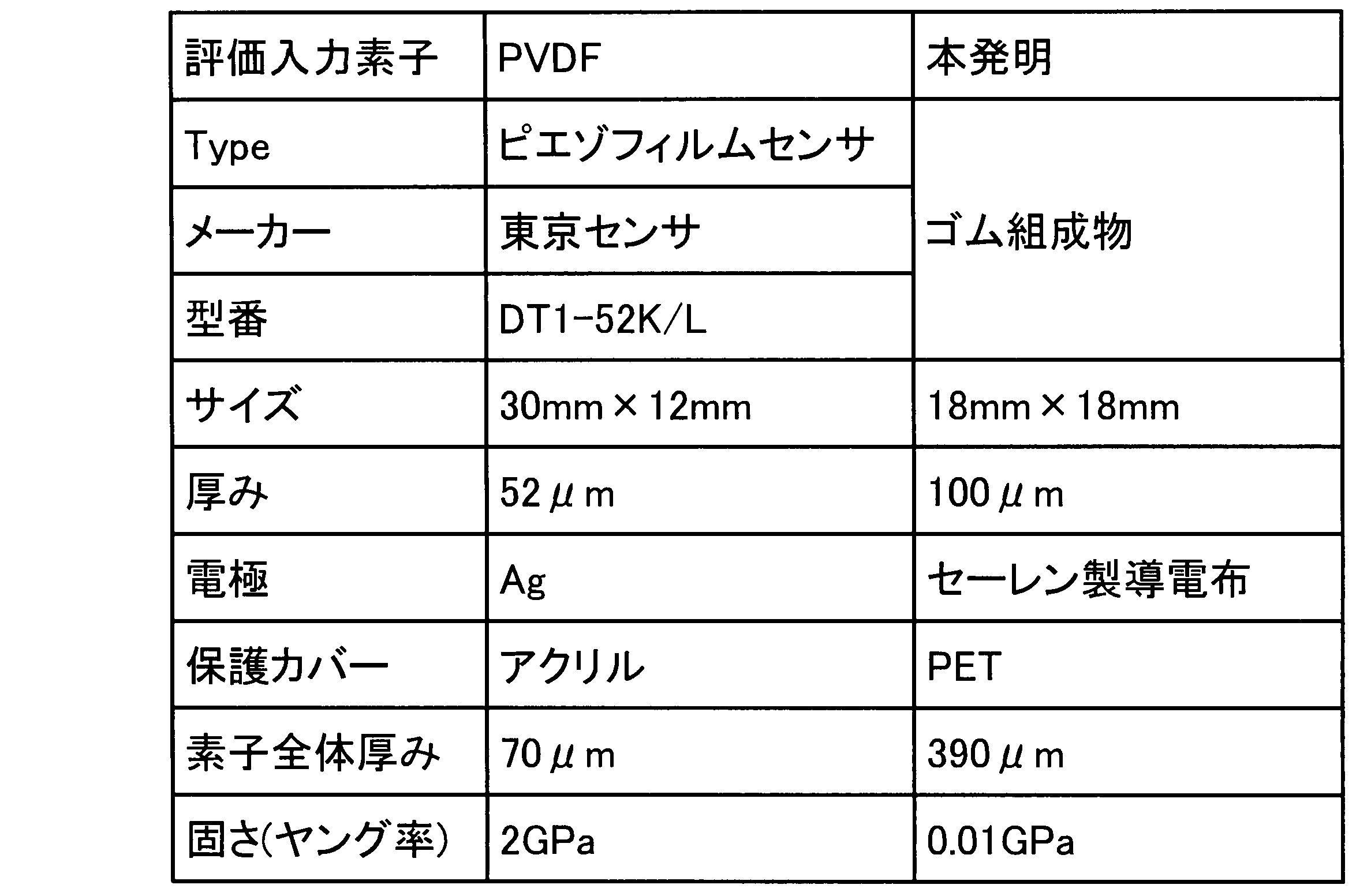

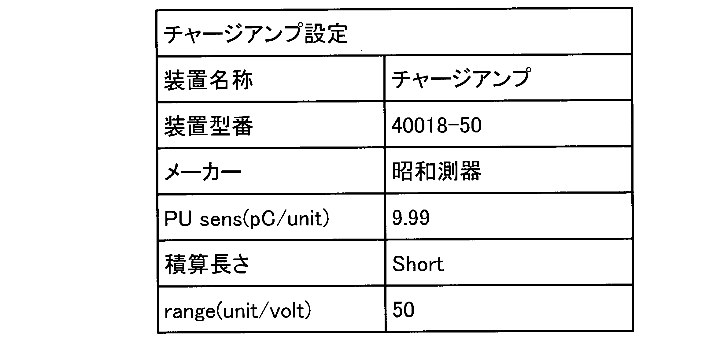


比較結果を図20及びその部分拡大図である図21に示す。ゴム組成物からなる中間層4を有する本実施形態の入力素子では、電圧信号の出力が、プローブ42に取り付けられたスポンジ44が入力素子に接触してから約0.01sec(10msec)後に開始している。
これに対し、PVDFを用いた入力素子では、約0.04sec(40msec)後に開始している。すなわち、本実施形態に係る入力素子に対して、約0.03sec(30msec)の遅延が生じている。
入力素子の感度において、この大きな遅延が生じる理由は、上記のようにPVDFは中間層4に比べてヤング率が大きく固いため、電圧信号の出力が開始する変形が生じるまで時間がかかるためである。
図22は、本実施形態の中間層4とPVDFのヤング率を測定し、信号出力開始時間との相関をプロットした図である。中間層のヤング率と信号出力開始時間はリニアな相関を持つことが確認された。
なお、中間層4のヤング率は、上述のゴム組成物の詳細な記載において硬度を測定している測定機(フィッシャー社製、超微小硬度計WIN-HUD)、及び同測定条件を用い、10μm深さの硬度より換算した値を用いている。
PVDF等を用いた従来の入力素子では、押圧力に対する出力が小さいので、信号増幅を行っている場合が多い。本発明の入力素子では出力が大きいので増幅が不要でより簡易な処理プロセスで機能を実現できる。
位置と押圧力を入力できることで、例えば、同一箇所へのタッチでも押圧力の強弱で複数のコマンドを使い分けたり、文字や図を筆圧を反映させて入力する等が可能になり、操作性を向上させることができる。
この場合、押圧力の違い(強弱)をはっきりと区別できることが要求されるが、PVDFを用いた入力素子では、押圧力に対する感度が低いため、押圧力の区別による操作性、機能性の向上は満足できる状況になかった。
また、本発明の入力素子は負荷耐久性も高いので、低圧力から高圧力まで広範囲で検知ができる。これにより、圧力の強弱を多段階で識別可能で処理機能の高い入力素子を提供できる。
表示素子と積層して使う場合、感度が高いので必ずしも本発明の入力素子を表示素子の最表層(操作側)に配置する必要はなく、素子構成の自由度が増す。また、本発明で用いる材料は耐熱性を有するので、プロセス温度の自由度が増す。
<入力素子の作製>
図26に示す断面構成を有する高温負荷評価用の入力素子108を、以下の手順で作製した。なお、高温負荷評価用の入力素子108は、入力素子101とカバーシート109から構成されており、入力素子101の断面構成は図25Bとし、入力素子101の外面はカバーシート109で覆われている構成とした。すなわち、評価対象の入力素子108は全てカバーシート109でパッケージングされている。
表面改質処理として、以下の条件でプラズマ処理(処理条件;ヤマト科学株式会社製、PR-500、出力100W、処理時間3分間、反応雰囲気:アルゴン99.999%、反応圧力10Pa)を施した。
表面改質処理後、中間層前駆体の処理面に、フッ素系炭素化合物(ダイキン工業株式会社製、オプツールDSX)をパーフルオロヘキサンで希釈した0.1%溶液を、引き上げ速度10mm/minのディッピング工法にて塗布した。その後、相対湿度90%、温度60℃の環境で30分間以上保持し、50℃で10分間乾燥させて、不活性化処理を施した。
第1の基板の電極面に、フィルムスペーサ(東レ株式会社製、U34ルミラー#50、厚み50μm)をL/S=1mm/9mmのストライプ状になるように、両面テープ(太陽金網株式会社製、TRAN-SIL NT-1001、厚さ50μm)で固定した。
第2の基板の電極面に、導電性両面テープ(太陽金網株式会社製、CHO-FOIL CCD、厚さ112μm)、中間層の順に重ねて貼り付けた。
第1および第2の基板にある各電極それぞれを引き出し電極に接続した。
二枚の基板を、第1の基板の電極面と第2の基板上の中間層が対向し、かつ電極のストライプ方向(長手方向)が直交するように重ね合わせ、両面テープ(太陽金網株式会社製、TRAN-SIL NT-1001、厚さ50μm)で固定して、実施例10の入力素子を作製した。
作製した入力素子の押圧に対する検出感度を評価した。評価は以下の手順で実施した。結果を表7に示す。表7の入力素子の欄における「図26/図25B」は、図25Bの断面構成を有する入力素子が図26に示すようにパッケージングされていることを示している。
実施例15における入力素子の断面構成は図23に示すものである。
実施例16と実施例17における入力素子の断面構成は図25Aに示すものである。
実施例18における入力素子の断面構成は図24Bに示すものである。
実施例19における入力素子の断面構成は図1に示すものであり、耐熱層を有しない本発明の基本構成をパッケージングした構成を有している。
(1)図27に示すように、高温負荷評価用の入力素子108を測定装置110のステージ111上に固定し、オシロスコープ112に接続する。
(2)プローブ113の先端にスポンジ114を取り付け、これを第1及び第2の電極の交点と中心が一致する位置に押し付ける。
(3)オシロスコープ112に表示された出力電圧を記録する。出力電圧は5回測定した平均値とする。
(4)後述する比較例2に対する出力電圧倍率を求め、検出感度をランク判定する。
測定装置:定着シミュレータFSR-1000(レスカ製)
測定パターン:荷重制御
押し付け速度:5mm/sec
押し付け荷重:300gf
押し付け保持時間:1sec
引き上げ速度:5mm/sec
プローブ径:直径10mm
スポンジ:シリコーンスポンジ、硬さ15、直径10mm、厚さ5mm
オシロスコープ:WaveAce1001(LeCroy製)
ランクA:比較例2に対して出力電圧が5倍以上
ランクB:比較例2に対して出力電圧が3倍以上
ランクC:比較例2に対して出力電圧が1倍以上
ランクD:比較例2に対して出力電圧が1倍未満
<入力素子の作製>
実施例10の入力素子において、中間層に高温負荷を加えたこと以外は、実施例10と同様にして、実施例11の入力素子を作製した。すなわち、図26/図25Bに示す断面構成を有する入力素子とした。
中間層を温度150℃の恒温器(ヤマト科学株式会社製、DN410H)に24時間保持して、高温負荷を加えた。その後、中間層を取り出して、24℃、40RH%の条件下で24時間静置保管した。
作製した実施例11の入力素子について、実施例10と同様にして、押圧に対する検出感度を評価した。結果を表7に示す。
表7から明らかなように、実施例11の中間層は高温負荷後に検出感度が低下するものの、比較例2に比べて検出感度が高く、十分な耐熱性を有していることがわかる。
すなわち、比較例2の入力素子では高温負荷後に検出感度が8割も低下しているのに対し、実施例11の入力素子では3割弱しか低下していない。このことは、炎天下での車中の温度上昇等の環境変動に十分に耐えることができ(ランクA、Bを維持)、スマートフォン等の電子機器の使用性の向上に寄与することを意味する。
<入力素子の作製>
実施例10の入力素子において、第2の基板にある電極面と中間層とを導電性接着剤(スリーボンド製、TB3303B、厚さ50μm、接着条件150℃で1時間)で加熱接着したこと以外は、実施例10と同様にして、実施例12の入力素子を作製した。すなわち、図26/図25Bに示す断面構成を有する入力素子とした。
作製した実施例12の入力素子について、実施例10と同様にして、押圧に対する検出感度を評価した。結果を表7に示す。
表7から明らかなように、実施例12の中間層は高温負荷後に検出感度が低下するものの、比較例2に比べて検出感度が高く、十分な耐熱性を有していることがわかる。これにより、入力素子の製造工程において、加熱接着を利用できる。製造段階で加熱接着できることにより、高信頼性につながる製造精度の向上を得ることができるとともに、製品化後の位相ずれによる信号相殺に起因する出力低下等の問題を抑制できる。
<入力素子の作製>
実施例10の入力素子に高温負荷を加えて、実施例13の入力素子とした。
(高温負荷)
入力素子を温度150℃の恒温器(ヤマト科学株式会社製、DN410H)に1時間保持して、高温負荷を加えた。その後、入力素子を取り出して、24℃、40RH%の条件下で1時間静置保管した。
作製した実施例13の入力素子について、実施例10と同様にして、押圧に対する検出感度を評価した。結果を表7に示す。
表7から明らかなように、実施例13の入力素子は高温負荷後に検出感度が低下するものの、比較例2に比べて検出感度が高く、十分な耐熱性を有していることがわかる。これにより、本発明の入力素子は高温環境においても使用できる。
<入力素子の作製>
実施例12の入力素子に高温負荷を加えて、実施例14の入力素子とした。
(高温負荷)
入力素子を温度150℃の恒温器(ヤマト科学株式会社製、DN410H)に1時間保持して、高温負荷を加えた。その後、入力素子を取り出して、24℃、40RH%の条件下で1時間静置保管した。
作製した実施例14の入力素子について、実施例10と同様にして、押圧に対する検出感度を評価した。結果を表7に示す。
表7から明らかなように、実施例14の入力素子は高温負荷後も高い検出感度を維持しており、十分な耐熱性を有していることがわかる。これにより、本発明の入力素子は高温環境においても使用できる。
<入力素子の作製>
実施例12の入力素子において、第1の基板にある電極面に接着層とスペーサを設けなかったこと以外は、実施例12と同様にして、実施例15の入力素子を作製した。すなわち、図26/図23に示す断面構成を有する入力素子とした。更に、入力素子に高温負荷を加えた。
入力素子を温度150℃の恒温器(ヤマト科学株式会社製、DN410H)に1時間保持して、高温負荷を加えた。その後、入力素子を取り出して、24℃、40RH%の条件下で1時間静置保管した。
作製した実施例15の入力素子について、実施例10と同様にして、押圧に対する検出感度を評価した。結果を表7に示す。
表7から明らかなように、実施例15の入力素子はスペーサを有する入力素子に比べて検出感度が低いものの、比較例2に比べると検出感度は高いことがわかる。換言すれば、電極と中間層との間に隙間を設け、あるいは非接着状態とすることにより、摩擦ないし剥離帯電を増加させ、大きな電気信号を得ることができる。
<入力素子の作製>
図26に示す断面構成を有する高温負荷評価用の入力素子108を、以下の手順で作製した。なお、高温負荷評価用の入力素子108は、入力素子101とカバーシート109から構成されており、入力素子101の断面構成は図25Aとし、入力素子101の外面はカバーシート109で覆われている構成とした。
PETフィルム上に、シリコーンゴム(モメンティブ・パフォーマンス・マテリアルズ・ジャパン合同会社製、TSE3033)100質量部、及びシリカ(日本アエロジル株式会社製、R972)10質量部とからなるシリコーンゴム組成物を塗布し、120℃で30分間加熱硬化させて、厚み100μmの中間層前駆体を形成した。更に、上記中間層前駆体に表面改質処理を施して、PETフィルムから剥がし、中間層を得た。
表面改質処理として、以下の条件でコロナ放電処理(処理条件;印加電圧100V、積算エネルギー:60J/cm2、反応雰囲気:空気)を施した。
次に、40mm×40mmに切り出したPET基板上に、L/S=8mm/2mmのストライプ状にITO電極を形成したものを二枚準備した。
第1の基板の電極面に、スペーサとして直径10μmの球状シリカをイソプロピルアルコール中に分散させたスペーサ散布液を、スピンコート機にて散布した。その後、乾燥させて、第1の基板の電極面にスペーサを設けた。
第1および第2の基板にある各電極それぞれを引き出し電極に接続した。
二枚の基板を、第1の基板の電極面と第2の基板上の中間層が対向し、かつ電極のストライプ方向(長手方向)が直交するように重ね合わせ、両面テープ(太陽金網株式会社製、TRAN-SIL NT-1001、厚さ50μm)で固定して、実施例16の入力素子を作製した。更に、入力素子に高温負荷を加えた。
入力素子を温度150℃の恒温器(ヤマト科学株式会社製、DN410H)に1時間保持して、高温負荷を加えた。その後、入力素子を取り出して、24℃、40RH%の条件下で1時間静置保管した。
作製した実施例16の入力素子について、実施例10と同様にして、押圧に対する検出感度を評価した。結果を表7に示す。
表7から明らかなように、実施例16の入力素子は高温負荷後も高い検出感度を示すことがわかる。
<入力素子の作製>
図26に示す断面構成を有する高温負荷評価用の入力素子108を、以下の手順で作製した。なお、高温負荷評価用の入力素子108は、入力素子101とカバーシート109から構成されており、入力素子101の断面構成は図25Aとし、入力素子101の外面はカバーシート109で覆われている構成とした。
PETフィルム上に、フロロシリコーンゴム(信越化学工業株式会社製、X36-420U)、及びチタン酸バリウム(ALDRICH社製、208108)30質量部とからなるシリコーンゴム組成物を塗布し、120℃で30分間加熱硬化させて、厚み100μmの中間層前駆体を形成した。更に、上記中間層前駆体に表面改質処理を施して、PETフィルムから剥がし、中間層を得た。
表面改質処理として、以下の条件でUV照射処理(処理条件;ヴィルバー・ルーマット社製、VL-215.C、波長254nm、積算光量300J/cm2、反応雰囲気:窒素、酸素分圧5,000ppm以下)を施した。
次に、40mm×40mmに切り出したPET基板上に、L/S=8mm/2mmのストライプ状にITO電極を形成したものを二枚準備した。
第1の基板の電極面に、スペーサとして直径10μmの球状シリカをイソプロピルアルコール中に分散させたスペーサ散布液を、スピンコート機にて散布した。その後、乾燥させて、第1の基板の電極面にスペーサを設けた。
第1および第2の基板にある各電極それぞれを引き出し電極に接続した。
二枚の基板を、第1の基板の電極面と第2の基板上の中間層が対向し、かつ電極のストライプ方向(長手方向)が直交するように重ね合わせ、両面テープ(太陽金網株式会社製、TRAN-SIL NT-1001、厚さ50μm)で固定して、実施例17の入力素子を作製した。更に、入力素子に高温負荷を加えた。
入力素子を温度150℃の恒温器(ヤマト科学株式会社製、DN410H)に1時間保持して、高温負荷を加えた。その後、入力素子を取り出して、24℃、40RH%の条件下で1時間静置保管した。
作製した実施例17の入力素子について、実施例10と同様にして、押圧に対する検出感度を評価した。結果を表7に示す。
表7から明らかなように、実施例17の入力素子は高温負荷後も高い検出感度を示すことがわかる。
<入力素子の作製>
図26に示す断面構成を有する高温負荷評価用の入力素子108を、以下の手順で作製した。なお、高温負荷評価用の入力素子108は、入力素子101とカバーシート109から構成されており、入力素子101の断面構成は図24Bとし、入力素子101の外面はカバーシート109で覆われている構成とした。
PETフィルム上に、シリコーンゴム(信越化学工業株式会社製、KE-1935)、及びチタン酸バリウム(ALDRICH社製、208108)50質量部とからなるシリコーンゴム組成物を塗布し、120℃で30分間加熱硬化させて、厚み100μmの中間層前駆体を形成した。更に、上記中間層前駆体に表面改質処理を施して、PETフィルムから剥がし、中間層を得た。
表面改質処理として、以下の条件で電子線照射処理(処理条件;浜松ホトニクス株式会社製、ライン照射型低エネルギー電子線照射源、照射量1MGy、反応雰囲気:窒素、酸素分圧5000ppm以下)を施した。
次に、40mm×40mmに切り出したPET基板上に、L/S=8mm/2mmのストライプ状にITO電極を形成したものを2枚準備した。
第1および第2の基板にある各電極それぞれを引き出し電極に接続した。
上記のようにして、実施例18の入力素子を作製した。更に、入力素子に高温負荷を加えた。
入力素子を温度150℃の恒温器(ヤマト科学株式会社製、DN410H)に1時間保持して、高温負荷を加えた。その後、入力素子を取り出して、24℃、40RH%の条件下で1時間静置保管した。
作製した実施例18の入力素子について、実施例10と同様にして、押圧に対する検出感度を評価した。結果を表7に示す。
表7から明らかなように、実施例18の入力素子は高温負荷後も高い検出感度を示すことがわかる。
<入力素子の作製>
図26に示す断面構成を有する高温負荷評価用の入力素子108を、以下の手順で作製した。なお、高温負荷評価用の入力素子108は、入力素子101とカバーシート109から構成されており、入力素子101の断面構成は図1とし、入力素子101の外面はカバーシート109で覆われている構成とした。すなわち、図1で示した耐熱層を有しない本発明の基本構成をパッケージングしたものである。
PETフィルム上に、シリコーンゴム(信越化学工業株式会社製、KE-1935)を塗布し、120℃で30分間加熱硬化させて、厚み100μmの中間層前駆体を形成した。更に、上記中間層前駆体に表面改質処理及び不活性化処理を施して、PETフィルムから剥がし、中間層を得た。
表面改質処理として、以下の条件でプラズマ処理(処理条件;ヤマト科学株式会社製、PR-500、出力100W、処理時間3分間、反応雰囲気:アルゴン99.999%、反応圧力10Pa)を施した。
表面改質処理後、中間層前駆体の処理面に、フッ素系炭素化合物(ダイキン工業株式会社製、オプツールDSX)をパーフルオロヘキサンで希釈した0.1%溶液を、引き上げ速度10mm/minのディッピング工法にて塗布した。その後、相対湿度90%、温度60℃の環境で30分間以上保持し、50℃で10分間乾燥させて、不活性化処理を施した。
第2の基板の電極面に、前記中間層、第1の基板の電極面の順に重ね、両面テープ(太陽金網株式会社製、TRAN-SIL NT-1001、厚さ50μm)で固定した。なお、第1の基板の電極面と第2の基板上の中間層が対向し、かつ電極のストライプ方向(長手方向)が直交するように重ね合わせた。
第1および第2の基板にある各電極それぞれを引き出し電極に接続した。
上記のようにして、実施例19の入力素子を作製した。更に、入力素子に高温負荷を加えた。
入力素子を温度150℃の恒温器(ヤマト科学株式会社製、DN410H)に1時間保持して、高温負荷を加えた。その後、入力素子を取り出して、24℃、40RH%の条件下で1時間静置保管した。
作製した実施例19の入力素子について、実施例10と同様にして、押圧に対する検出感度を評価した。結果を表7に示す。
<入力素子の作製>
実施例10の入力素子において、中間層をPVDF(東京センサ株式会社製、厚み110μm)に変えたこと以外は、実施例10と同様にして、比較例2の入力素子を作製した。すなわち、図26/図25Bに示す断面構成を有する入力素子とした。
作製した比較例2の入力素子について、実施例10と同様にして、押圧に対する検出感度を評価した。結果を表7に示す。
表7から明らかなように、比較例2の入力素子は高温負荷がかからない状態での比較においても本発明の入力素子に比べて検出感度が低いことがわかる。
<入力素子の作製>
比較例2の入力素子において、中間層に高温負荷を加えたこと以外は、比較例2と同様にして、比較例3の入力素子を作製した。すなわち、図26/図25Bに示す断面構成を有する入力素子とした。
中間層を温度150℃の恒温器(ヤマト科学株式会社製、DN410H)に24時間保持して、高温負荷を加えた。その後、中間層を取り出して、24℃、40RH%の条件下で24時間静置保管した。
作製した比較例3の入力素子について、実施例10と同様にして、押圧に対する検出感度を評価した。結果を表7に示す。
表7から明らかなように、比較例3の中間層は高温負荷後に検出感度が著しく低下することがわかる。このことは、炎天下での車中の温度上昇等の環境変動に十分に耐えることができず、場合によっては使用不可となり得ることを意味する。
<入力素子の作製>
比較例2の入力素子において、第2の基板にある電極面と中間層とを導電性接着剤(スリーボンド製、TB3303B、厚さ50μm、接着条件150℃で1時間)で加熱接着したこと以外は、比較例2と同様にして、比較例4の入力素子を作製した。すなわち、図26/図25Bに示す断面構成を有する入力素子とした。
作製した比較例4の入力素子について、実施例10と同様にして、押圧に対する検出感度を評価した。結果を表7に示す。
表7から明らかなように、比較例4の中間層は高温負荷後に検出感度が著しく低下することがわかる。
<入力素子の作製>
比較例2の入力素子に高温負荷を加えて、比較例5の入力素子とした。
(高温負荷)
入力素子を温度150℃の恒温器(ヤマト科学株式会社製、DN410H)に1時間保持して、高温負荷を加えた。その後、入力素子を取り出して、24℃、40RH%の条件下で1時間静置保管した。
作製した比較例5の入力素子について、実施例10と同様にして、押圧に対する検出感度を評価した。結果を表7に示す。
表7から明らかなように、比較例5の入力素子は高温負荷後に検出感度が著しく低下することがわかる。
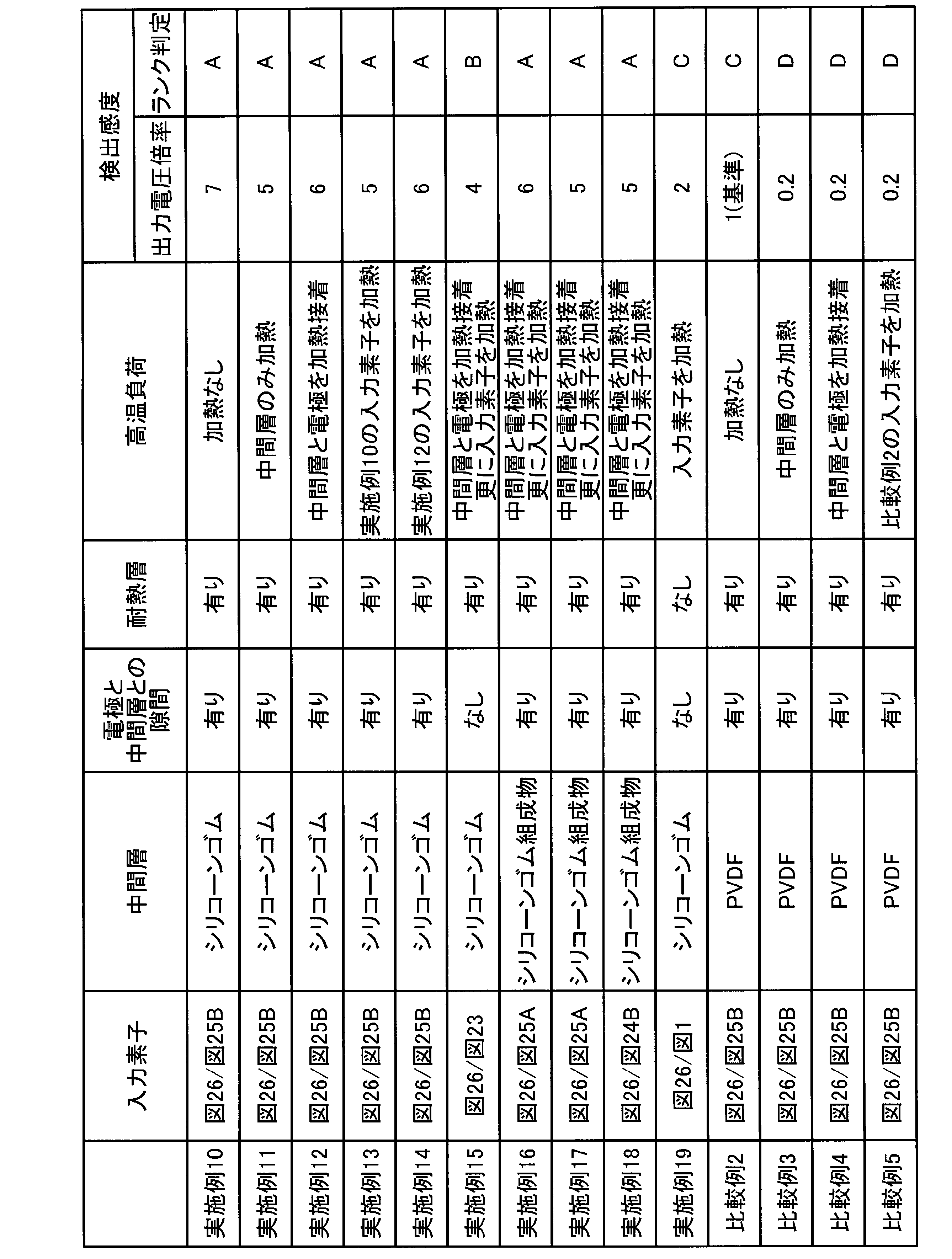
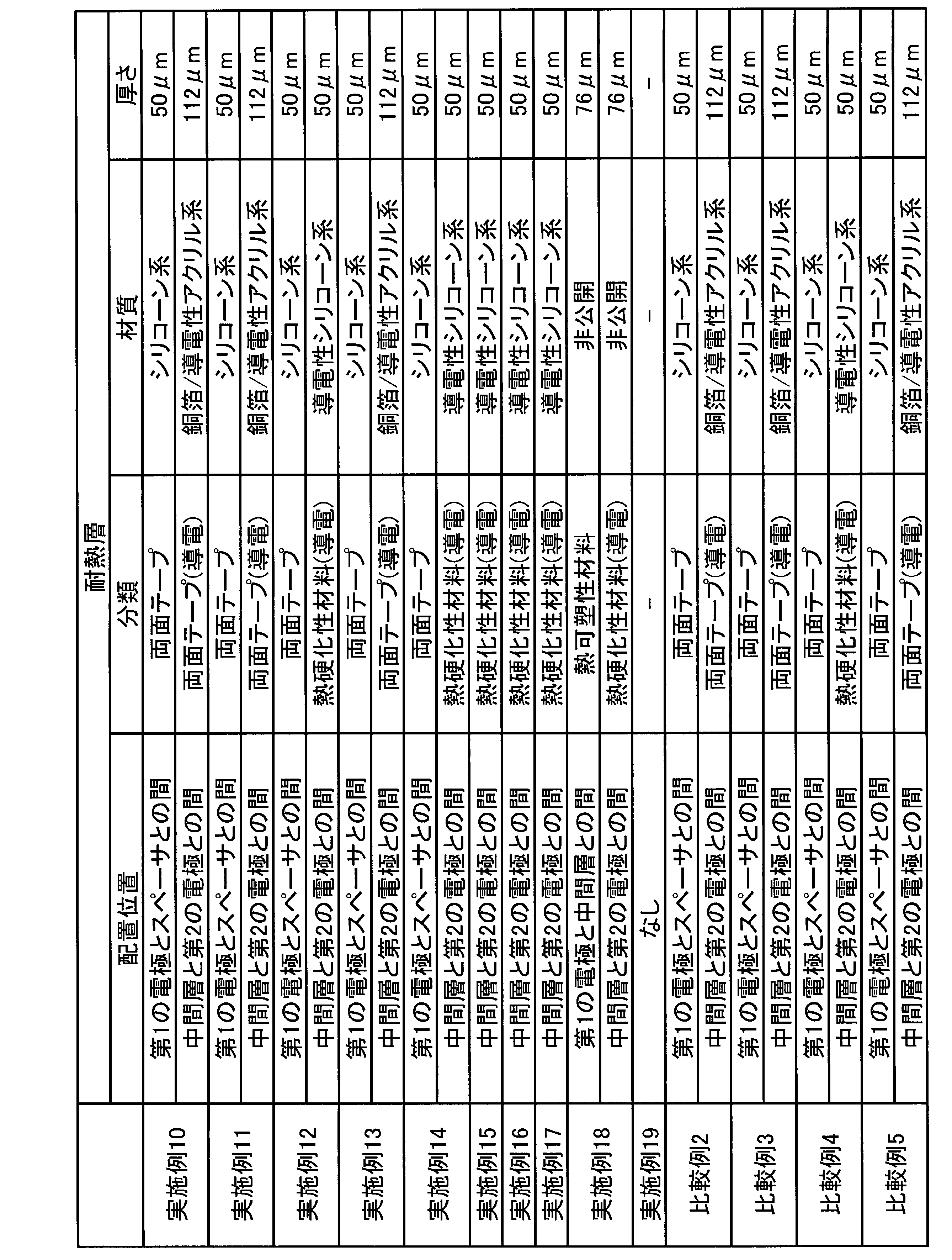
実施例14では、中間層104と第2の電極103との間が導電性シリコーン系の熱硬化性材料で加熱接着されており、入力素子全体を加熱している。
実施例14では加熱負荷が多いにも拘わらず、加熱負荷の少ない実施例13よりも出力電圧の倍率が高い。このことは、中間層104の材質(シリコーン)と、耐熱層105の材質とが実施例14では熱特性が同一又は同等のものとなっていることも一因と考えられる。
すなわち、高温負荷による熱膨張率の違いに基づく界面剥離や位相ずれによる信号相殺等が高精度に抑制されるからであると考えられる。
本発明の実施の形態に記載された効果は、本発明から生じる最も好適な効果を例示したに過ぎず、本発明による効果は、本発明の実施の形態に記載されたものに限定されるものではない。
2、102 第1の電極
3、103 第2の電極
4、104 中間層
5 入力装置
6 表示素子
8 信号処理部
8A 位置検出部
8B 圧力検出部
23、107 スペーサ
105 耐熱層
Claims (10)
- 互いに対向する第1及び第2の電極と、
第1及び第2の電極間に配置され、シロキサンを含有するゴムまたはゴム組成物で形成された中間層と、
を備えている入力素子。 - 請求項1に記載の入力素子において、
第1及び第2の電極の少なくとも一方と前記中間層との間、あるいは第1及び第2の電極の少なくとも一方の前記中間層と反対側に配置される耐熱層とを備えている入力素子。 - 請求項2に記載の入力素子において、
前記耐熱層が熱硬化性材料または熱可塑性材料で形成され、接着層としての機能を有している入力素子。 - 請求項3に記載の入力素子において、
前記耐熱層は前記中間層と熱特性が同一又は同等の材料で形成されている入力素子。 - 請求項1乃至4の何れか1つに記載の入力素子において、
前記中間層は、3つ~4つの酸素原子と結合したケイ素原子を有するシロキサンを含有するゴムまたはゴム組成物で形成されている入力素子。 - 請求項1乃至5の何れか1つに記載の入力素子において、
前記中間層は、その厚み方向の一方側から他方側へ向かって酸素が増加して極大値を持ち、且つ、前記一方側から他方側へ向かって炭素が減少して極小値を持つ濃度プロファイルを有する入力素子。 - 請求項1乃至6の何れか1つに記載の入力素子において、
前記中間層と、第1及び第2の電極の少なくとも一方とは、互いに接合されていない部分を有する入力素子。 - 請求項7に記載の入力素子において、
前記中間層と、第1及び第2の電極の少なくとも一方との間にスペーサを有する入力素子。 - 請求項1乃至8の何れか1つに記載の入力素子において、
第1の電極は第1の方向に沿って配列した複数の電極からなり、第2の電極は第1の方向と直交する第2の方向に沿って配列した複数の電極からなる入力素子。 - 請求項1乃至9の何れか1つに記載の入力素子と、
前記中間層が押圧されることで発生する電気信号を処理する信号処理部と、
を備えた入力装置。
Priority Applications (5)
| Application Number | Priority Date | Filing Date | Title |
|---|---|---|---|
| CN201780016603.2A CN108780370B (zh) | 2016-03-14 | 2017-01-16 | 输入元件和输入装置 |
| KR1020187026434A KR102154136B1 (ko) | 2016-03-14 | 2017-01-16 | 입력 소자 및 입력 장치 |
| EP17766031.3A EP3432127B1 (en) | 2016-03-14 | 2017-01-16 | Input element and input device |
| JP2018505286A JP6624279B2 (ja) | 2016-03-14 | 2017-01-16 | 入力素子及び入力装置 |
| US16/083,722 US11010004B2 (en) | 2016-03-14 | 2017-01-16 | Input element and input device |
Applications Claiming Priority (4)
| Application Number | Priority Date | Filing Date | Title |
|---|---|---|---|
| JP2016-049588 | 2016-03-14 | ||
| JP2016049588 | 2016-03-14 | ||
| JP2016-246273 | 2016-12-20 | ||
| JP2016246273 | 2016-12-20 |
Publications (1)
| Publication Number | Publication Date |
|---|---|
| WO2017159023A1 true WO2017159023A1 (ja) | 2017-09-21 |
Family
ID=59850209
Family Applications (1)
| Application Number | Title | Priority Date | Filing Date |
|---|---|---|---|
| PCT/JP2017/001251 WO2017159023A1 (ja) | 2016-03-14 | 2017-01-16 | 入力素子及び入力装置 |
Country Status (6)
| Country | Link |
|---|---|
| US (1) | US11010004B2 (ja) |
| EP (1) | EP3432127B1 (ja) |
| JP (1) | JP6624279B2 (ja) |
| KR (1) | KR102154136B1 (ja) |
| CN (1) | CN108780370B (ja) |
| WO (1) | WO2017159023A1 (ja) |
Cited By (2)
| Publication number | Priority date | Publication date | Assignee | Title |
|---|---|---|---|---|
| WO2020065420A1 (en) * | 2018-08-31 | 2020-04-02 | Sabic Global Technologies B.V. | User input device with capacitive and triboeuectric sensors |
| CN111954797A (zh) * | 2018-04-05 | 2020-11-17 | 大陆轮胎德国有限公司 | 包括用于测量机械力的设备的充气轮胎、及该设备的用途 |
Families Citing this family (4)
| Publication number | Priority date | Publication date | Assignee | Title |
|---|---|---|---|---|
| WO2016193432A1 (en) * | 2015-06-03 | 2016-12-08 | Koninklijke Philips N.V. | Actuator device and array of the same |
| EP3410089B1 (en) * | 2016-01-29 | 2020-12-02 | Ricoh Company, Ltd. | Pressure-sensitive sensor, gripping device, and robot |
| KR102648676B1 (ko) * | 2018-04-27 | 2024-03-18 | 삼성디스플레이 주식회사 | 입력 감지 장치 및 이를 포함하는 표시 장치 |
| JP2021064690A (ja) * | 2019-10-11 | 2021-04-22 | 株式会社リコー | 素子および素子の製造方法 |
Citations (5)
| Publication number | Priority date | Publication date | Assignee | Title |
|---|---|---|---|---|
| WO2009096419A1 (ja) * | 2008-01-28 | 2009-08-06 | Kuraray Co., Ltd. | 可撓性を有する変形センサ |
| JP4784041B2 (ja) | 2003-11-07 | 2011-09-28 | パナソニック株式会社 | タッチパネルを用いた入力装置 |
| WO2014017184A1 (ja) * | 2012-07-25 | 2014-01-30 | 株式会社ビスキャス | 振動発電体およびその製造方法 |
| JP2014186711A (ja) | 2013-02-23 | 2014-10-02 | Nissha Printing Co Ltd | 押圧力測定を備えたタッチパネル |
| US20150292964A1 (en) * | 2012-10-08 | 2015-10-15 | Stc.Unm | Pliable Pressure-Sensing Fabric |
Family Cites Families (20)
| Publication number | Priority date | Publication date | Assignee | Title |
|---|---|---|---|---|
| US5616646A (en) * | 1994-11-07 | 1997-04-01 | Genesee Polymers Corporation | Restructuring silicone rubber to produce fluid or grease |
| US6809280B2 (en) | 2002-05-02 | 2004-10-26 | 3M Innovative Properties Company | Pressure activated switch and touch panel |
| US9018030B2 (en) * | 2008-03-20 | 2015-04-28 | Symbol Technologies, Inc. | Transparent force sensor and method of fabrication |
| JP2011155077A (ja) * | 2010-01-26 | 2011-08-11 | Renesas Electronics Corp | 半導体装置の製造方法 |
| JP5498811B2 (ja) | 2010-02-17 | 2014-05-21 | アルプス電気株式会社 | 静電容量式の入力装置 |
| JP5652611B2 (ja) * | 2011-03-02 | 2015-01-14 | 株式会社リコー | 定着部材、定着装置及び画像形成装置 |
| CN107742670B (zh) | 2011-04-08 | 2020-06-23 | 株式会社村田制作所 | 操作设备 |
| DE102012212222B4 (de) | 2012-03-12 | 2018-05-30 | Fraunhofer-Gesellschaft zur Förderung der angewandten Forschung e.V. | Dielektrisches Elastomer auf Fluorosilicon-Basis und Verfahren zu seiner Herstellung |
| CN114089600A (zh) * | 2012-03-15 | 2022-02-25 | 富士胶片株式会社 | 静电电容型输入装置及其制造方法、图像显示装置 |
| CA2894003A1 (en) | 2012-12-05 | 2014-06-12 | Danmarks Tekniske Universitet | Dielectric electroactive polymers comprising an ionic supramolecular structure |
| TW201431966A (zh) * | 2012-12-28 | 2014-08-16 | Dow Corning | 轉換器及其製造方法 |
| JP2015097068A (ja) | 2013-10-08 | 2015-05-21 | ダイキン工業株式会社 | タッチ入力装置および電子機器 |
| US20160378223A1 (en) * | 2013-12-18 | 2016-12-29 | Shin-Etsu Polymer Co., Ltd. | Detection sensor and detection sensor fabrication method |
| US9606652B2 (en) * | 2014-06-23 | 2017-03-28 | Eastman Kodak Company | Electronic devices and precursor articles |
| JP6870200B2 (ja) | 2014-11-13 | 2021-05-12 | 株式会社リコー | 素子、及び発電装置 |
| JP6540125B2 (ja) | 2015-03-18 | 2019-07-10 | 株式会社リコー | 発電素子及び発電装置 |
| US10248241B2 (en) * | 2015-05-07 | 2019-04-02 | Ricoh Company, Ltd. | Digital signage system |
| US10305020B2 (en) | 2015-05-15 | 2019-05-28 | Ricoh Company, Ltd. | Element and electric generator |
| JP6544037B2 (ja) | 2015-05-18 | 2019-07-17 | 株式会社リコー | 発電素子ユニット、及び発電装置 |
| JP2016218622A (ja) | 2015-05-18 | 2016-12-22 | 株式会社リコー | 誘導装置、及び誘導システム |
-
2017
- 2017-01-16 US US16/083,722 patent/US11010004B2/en active Active
- 2017-01-16 KR KR1020187026434A patent/KR102154136B1/ko active IP Right Grant
- 2017-01-16 CN CN201780016603.2A patent/CN108780370B/zh active Active
- 2017-01-16 JP JP2018505286A patent/JP6624279B2/ja active Active
- 2017-01-16 EP EP17766031.3A patent/EP3432127B1/en active Active
- 2017-01-16 WO PCT/JP2017/001251 patent/WO2017159023A1/ja active Application Filing
Patent Citations (5)
| Publication number | Priority date | Publication date | Assignee | Title |
|---|---|---|---|---|
| JP4784041B2 (ja) | 2003-11-07 | 2011-09-28 | パナソニック株式会社 | タッチパネルを用いた入力装置 |
| WO2009096419A1 (ja) * | 2008-01-28 | 2009-08-06 | Kuraray Co., Ltd. | 可撓性を有する変形センサ |
| WO2014017184A1 (ja) * | 2012-07-25 | 2014-01-30 | 株式会社ビスキャス | 振動発電体およびその製造方法 |
| US20150292964A1 (en) * | 2012-10-08 | 2015-10-15 | Stc.Unm | Pliable Pressure-Sensing Fabric |
| JP2014186711A (ja) | 2013-02-23 | 2014-10-02 | Nissha Printing Co Ltd | 押圧力測定を備えたタッチパネル |
Non-Patent Citations (1)
| Title |
|---|
| See also references of EP3432127A4 |
Cited By (7)
| Publication number | Priority date | Publication date | Assignee | Title |
|---|---|---|---|---|
| CN111954797A (zh) * | 2018-04-05 | 2020-11-17 | 大陆轮胎德国有限公司 | 包括用于测量机械力的设备的充气轮胎、及该设备的用途 |
| JP2021517093A (ja) * | 2018-04-05 | 2021-07-15 | コンチネンタル・ライフェン・ドイチュラント・ゲゼルシャフト・ミト・ベシュレンクテル・ハフツング | 機械力測定装置を含むタイヤ及び前記装置の使用 |
| US11415471B2 (en) | 2018-04-05 | 2022-08-16 | Continental Reifen Deutschland Gmbh | Tire comprising a device, wherein said device has a first, second, third, fourth and fifth layer, and uses of the device |
| JP7136914B2 (ja) | 2018-04-05 | 2022-09-13 | コンチネンタル・ライフェン・ドイチュラント・ゲゼルシャフト・ミト・ベシュレンクテル・ハフツング | 機械力測定装置を含むタイヤ及び前記装置の使用 |
| US11624665B2 (en) | 2018-04-05 | 2023-04-11 | Continental Reifen Deutschland Gmbh | Pneumatic tire comprising a device for measuring a mechanical force and use of the device |
| US11821799B2 (en) | 2018-04-05 | 2023-11-21 | Continental Reifen Deutschland Gmbh | Pneumatic tire comprising a device for measuring a mechanical force and use of the device |
| WO2020065420A1 (en) * | 2018-08-31 | 2020-04-02 | Sabic Global Technologies B.V. | User input device with capacitive and triboeuectric sensors |
Also Published As
| Publication number | Publication date |
|---|---|
| CN108780370B (zh) | 2021-10-15 |
| US11010004B2 (en) | 2021-05-18 |
| US20190089353A1 (en) | 2019-03-21 |
| EP3432127A4 (en) | 2019-03-20 |
| KR20180108836A (ko) | 2018-10-04 |
| JP6624279B2 (ja) | 2019-12-25 |
| EP3432127A1 (en) | 2019-01-23 |
| KR102154136B1 (ko) | 2020-09-09 |
| EP3432127B1 (en) | 2022-03-09 |
| JPWO2017159023A1 (ja) | 2018-09-27 |
| CN108780370A (zh) | 2018-11-09 |
Similar Documents
| Publication | Publication Date | Title |
|---|---|---|
| WO2017159023A1 (ja) | 入力素子及び入力装置 | |
| KR102176966B1 (ko) | 감압 센서, 파지 장치 및 로봇 | |
| US10714676B2 (en) | Sensor and sensor system | |
| KR102115870B1 (ko) | 소자, 셀, 및 발전 디바이스 | |
| US9632542B2 (en) | Touch screens comprising graphene layers | |
| TWI609837B (zh) | 保形元件之製造方法、保形元件及其用途 | |
| TW201514817A (zh) | 觸控視窗及包括該觸控視窗之觸控式裝置 | |
| TW201131442A (en) | Touch panel and mobile device utilizing touch panel | |
| JP6493622B2 (ja) | 非常停止用感圧センサ、安全装置及び安全システム | |
| US20130181925A1 (en) | Touch panel | |
| US8237670B2 (en) | Touch panel and display device using the same | |
| JP2017135775A (ja) | 発電素子及び発電装置 | |
| CN106598347A (zh) | 力感测装置及oled显示装置 | |
| TWI652603B (zh) | 觸控感應元件以及包含其的顯示裝置 | |
| US20150070600A1 (en) | Sensor device, method of manufacturing sensor device, display apparatus, and input apparatus | |
| KR20110090397A (ko) | 그래핀 패턴 형성 장치 및 방법 | |
| JPWO2009025085A1 (ja) | 透明タッチパネルとその製造方法 | |
| JP2018087801A (ja) | センサ及びセンサシステム | |
| JP2012064211A (ja) | 静電容量方式タッチスクリーンの製造方法 | |
| JP6808979B2 (ja) | 入力素子及び入力装置 | |
| US11150107B1 (en) | Touch sensor | |
| TW201122629A (en) | Touch panel | |
| US11507240B2 (en) | Touch sensor | |
| JP2022147757A (ja) | 素子 | |
| JP2012221449A (ja) | タッチパネル |
Legal Events
| Date | Code | Title | Description |
|---|---|---|---|
| ENP | Entry into the national phase |
Ref document number: 2018505286 Country of ref document: JP Kind code of ref document: A |
|
| ENP | Entry into the national phase |
Ref document number: 20187026434 Country of ref document: KR Kind code of ref document: A |
|
| WWE | Wipo information: entry into national phase |
Ref document number: 1020187026434 Country of ref document: KR |
|
| NENP | Non-entry into the national phase |
Ref country code: DE |
|
| WWE | Wipo information: entry into national phase |
Ref document number: 2017766031 Country of ref document: EP |
|
| ENP | Entry into the national phase |
Ref document number: 2017766031 Country of ref document: EP Effective date: 20181015 |
|
| 121 | Ep: the epo has been informed by wipo that ep was designated in this application |
Ref document number: 17766031 Country of ref document: EP Kind code of ref document: A1 |