WO2017158886A1 - 光変調器、及び光変調器を用いた光送信装置 - Google Patents
光変調器、及び光変調器を用いた光送信装置 Download PDFInfo
- Publication number
- WO2017158886A1 WO2017158886A1 PCT/JP2016/077463 JP2016077463W WO2017158886A1 WO 2017158886 A1 WO2017158886 A1 WO 2017158886A1 JP 2016077463 W JP2016077463 W JP 2016077463W WO 2017158886 A1 WO2017158886 A1 WO 2017158886A1
- Authority
- WO
- WIPO (PCT)
- Prior art keywords
- optical
- surface acoustic
- bias
- substrate
- electrode
- Prior art date
- Legal status (The legal status is an assumption and is not a legal conclusion. Google has not performed a legal analysis and makes no representation as to the accuracy of the status listed.)
- Ceased
Links
Images






Classifications
-
- G—PHYSICS
- G02—OPTICS
- G02F—OPTICAL DEVICES OR ARRANGEMENTS FOR THE CONTROL OF LIGHT BY MODIFICATION OF THE OPTICAL PROPERTIES OF THE MEDIA OF THE ELEMENTS INVOLVED THEREIN; NON-LINEAR OPTICS; FREQUENCY-CHANGING OF LIGHT; OPTICAL LOGIC ELEMENTS; OPTICAL ANALOGUE/DIGITAL CONVERTERS
- G02F1/00—Devices or arrangements for the control of the intensity, colour, phase, polarisation or direction of light arriving from an independent light source, e.g. switching, gating or modulating; Non-linear optics
- G02F1/01—Devices or arrangements for the control of the intensity, colour, phase, polarisation or direction of light arriving from an independent light source, e.g. switching, gating or modulating; Non-linear optics for the control of the intensity, phase, polarisation or colour
- G02F1/0121—Operation of devices; Circuit arrangements, not otherwise provided for in this subclass
- G02F1/0123—Circuits for the control or stabilisation of the bias voltage, e.g. automatic bias control [ABC] feedback loops
-
- G—PHYSICS
- G02—OPTICS
- G02F—OPTICAL DEVICES OR ARRANGEMENTS FOR THE CONTROL OF LIGHT BY MODIFICATION OF THE OPTICAL PROPERTIES OF THE MEDIA OF THE ELEMENTS INVOLVED THEREIN; NON-LINEAR OPTICS; FREQUENCY-CHANGING OF LIGHT; OPTICAL LOGIC ELEMENTS; OPTICAL ANALOGUE/DIGITAL CONVERTERS
- G02F1/00—Devices or arrangements for the control of the intensity, colour, phase, polarisation or direction of light arriving from an independent light source, e.g. switching, gating or modulating; Non-linear optics
- G02F1/01—Devices or arrangements for the control of the intensity, colour, phase, polarisation or direction of light arriving from an independent light source, e.g. switching, gating or modulating; Non-linear optics for the control of the intensity, phase, polarisation or colour
- G02F1/21—Devices or arrangements for the control of the intensity, colour, phase, polarisation or direction of light arriving from an independent light source, e.g. switching, gating or modulating; Non-linear optics for the control of the intensity, phase, polarisation or colour by interference
- G02F1/225—Devices or arrangements for the control of the intensity, colour, phase, polarisation or direction of light arriving from an independent light source, e.g. switching, gating or modulating; Non-linear optics for the control of the intensity, phase, polarisation or colour by interference in an optical waveguide structure
-
- G—PHYSICS
- G02—OPTICS
- G02F—OPTICAL DEVICES OR ARRANGEMENTS FOR THE CONTROL OF LIGHT BY MODIFICATION OF THE OPTICAL PROPERTIES OF THE MEDIA OF THE ELEMENTS INVOLVED THEREIN; NON-LINEAR OPTICS; FREQUENCY-CHANGING OF LIGHT; OPTICAL LOGIC ELEMENTS; OPTICAL ANALOGUE/DIGITAL CONVERTERS
- G02F1/00—Devices or arrangements for the control of the intensity, colour, phase, polarisation or direction of light arriving from an independent light source, e.g. switching, gating or modulating; Non-linear optics
- G02F1/01—Devices or arrangements for the control of the intensity, colour, phase, polarisation or direction of light arriving from an independent light source, e.g. switching, gating or modulating; Non-linear optics for the control of the intensity, phase, polarisation or colour
- G02F1/21—Devices or arrangements for the control of the intensity, colour, phase, polarisation or direction of light arriving from an independent light source, e.g. switching, gating or modulating; Non-linear optics for the control of the intensity, phase, polarisation or colour by interference
- G02F1/212—Mach-Zehnder type
-
- G—PHYSICS
- G02—OPTICS
- G02F—OPTICAL DEVICES OR ARRANGEMENTS FOR THE CONTROL OF LIGHT BY MODIFICATION OF THE OPTICAL PROPERTIES OF THE MEDIA OF THE ELEMENTS INVOLVED THEREIN; NON-LINEAR OPTICS; FREQUENCY-CHANGING OF LIGHT; OPTICAL LOGIC ELEMENTS; OPTICAL ANALOGUE/DIGITAL CONVERTERS
- G02F2201/00—Constructional arrangements not provided for in groups G02F1/00 - G02F7/00
- G02F2201/12—Constructional arrangements not provided for in groups G02F1/00 - G02F7/00 electrode
-
- G—PHYSICS
- G02—OPTICS
- G02F—OPTICAL DEVICES OR ARRANGEMENTS FOR THE CONTROL OF LIGHT BY MODIFICATION OF THE OPTICAL PROPERTIES OF THE MEDIA OF THE ELEMENTS INVOLVED THEREIN; NON-LINEAR OPTICS; FREQUENCY-CHANGING OF LIGHT; OPTICAL LOGIC ELEMENTS; OPTICAL ANALOGUE/DIGITAL CONVERTERS
- G02F2201/00—Constructional arrangements not provided for in groups G02F1/00 - G02F7/00
- G02F2201/58—Arrangements comprising a monitoring photodetector
-
- G—PHYSICS
- G02—OPTICS
- G02F—OPTICAL DEVICES OR ARRANGEMENTS FOR THE CONTROL OF LIGHT BY MODIFICATION OF THE OPTICAL PROPERTIES OF THE MEDIA OF THE ELEMENTS INVOLVED THEREIN; NON-LINEAR OPTICS; FREQUENCY-CHANGING OF LIGHT; OPTICAL LOGIC ELEMENTS; OPTICAL ANALOGUE/DIGITAL CONVERTERS
- G02F2202/00—Materials and properties
- G02F2202/20—LiNbO3, LiTaO3
Definitions
- the present invention relates to an optical modulator and an optical transmitter using the optical modulator, and in particular, an optical modulator in which a bias electrode and a photodetector for monitoring emitted light are formed on the same substrate, and such an optical modulator.
- the present invention relates to an optical transmission device using an optical modulator.
- an optical transmission device incorporating a waveguide type optical modulator is often used.
- an optical modulator using LiNbO 3 (hereinafter also referred to as LN) having an electro-optic effect as a substrate uses a semiconductor material such as indium phosphide (InP), silicon (Si), or gallium arsenide (GaAs).
- the optical loss characteristic is small and a wide-band optical modulation characteristic can be realized. Therefore, it is widely used in high-speed / large-capacity optical fiber communication systems.
- a bias electrode for performing As such a bias electrode, for example, a bias electrode for applying an electric field to the optical waveguide in order to compensate for fluctuations in a bias point (so-called temperature drift phenomenon) caused by a temperature change in the environment, or for performing optical phase adjustment. There are bias electrodes.
- the modulation scheme in the optical fiber communication system has received a trend of increasing transmission capacity in recent years, such as QPSK (QuadratureKPhase Shift Keying) and DP-QPSK (Dual Polarization-Quadrature Phase Shift Keying).
- QPSK QuadratureKPhase Shift Keying
- DP-QPSK Double Polarization-Quadrature Phase Shift Keying
- An optical modulator that performs QPSK modulation (QPSK modulator) and an optical modulator that performs DP-QPSK modulation (DP-QPSK modulator) include a plurality of nested Mach-Zehnder optical waveguides, a plurality of high-frequency signal electrodes, Since the bias electrode is provided (see, for example, Patent Document 1), the device size tends to increase, and the demand for downsizing is particularly strong.
- the bias electrode is configured as a comb electrode (or interdigital electrode) composed of a push electrode and a pull electrode, and the voltage (bias voltage) to be applied to the bias electrode is reduced.
- the configuration is known (see, for example, Patent Document 2).
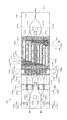
- FIG. 13 is a diagram showing an example of the configuration of a conventional DP-QPSK modulator.
- the DP-QPSK modulator 1300 is composed of, for example, a nested Mach-Zehnder optical waveguide (shown by a thick dotted line) formed on a Z-cut LN substrate 1302 and an electrode (shown by a hatched portion).
- a light source such as a laser diode is incident from the right in the figure, and the modulated light is emitted from the left in the figure.
- the emitted light is combined by, for example, a spatial optical system and is incident on an optical fiber connected to the optical transmission path.
- the optical waveguide modulates the incident waveguide 1304 that receives incident light from the right direction in the drawing, the optical branching unit 1306 that branches light propagating through the incident waveguide, and the light branched by the optical branching unit 1306. It is composed of two Mach-Zehnder optical waveguide portions 1310a and 1310b.
- the Mach-Zehnder optical waveguide section 1310a includes an incident waveguide 1312a, an optical branching section 1314a that branches light propagating through the incident waveguide 1312a, and a parallel waveguide 1316a that propagates the respective lights branched by the optical branching section 1314a, 1318a, a multiplexing unit 1320a for multiplexing the light propagated through the parallel waveguides 1316a and 1318a, and an output waveguide 1322a for emitting the light combined by the multiplexing unit 1320a to the outside.
- the Mach-Zehnder optical waveguide portion 1310a includes Mach-Zehnder optical waveguides 1330a (portions in a rectangle indicated by a dotted line in the figure) and 1332a (parts in a rectangle indicated by a two-dot chain line in the figure) respectively formed in a part of the parallel waveguides 1316a and 1318a. Part).
- Electrodes are respectively provided on the light exit sides (left side in the figure) of the parallel waveguides 1334a and 1336a of the Mach-Zehnder optical waveguide 1330a and on the light exit side (left side in the figure) of the parallel waveguides 1338a and 1340a of the Mach-Zehnder optical waveguide 1332a.
- a bias electrode 1346a composed of 1342a and 1344a and a bias electrode 1352a composed of electrodes 1348a and 1350a are formed.
- a bias electrode 1358a composed of electrodes 1354a and 1356a is formed on the light exit side (left side in the drawing) of the parallel waveguides 1316a and 1318a of the Mach-Zehnder optical waveguide portion 1310a.
- the optical modulator 1300 includes six bias electrodes indicated by reference numerals 1346a, 1352a, 1358a, 1346b, 1352b, and 1358b. Also, the optical modulator 1300 includes electrodes 1370, 8 on 8 parallel waveguides 1334a, 1336a, 1338a, 1340a, 1334b, 1336b, 1338b, 1340b of four Mach-Zehnder optical waveguides 1330a, 1332a, 1330b, 1332b, respectively. RF electrodes composed of 1372, 1374, 1376, 1378, 1380, 1382, 1384, 1386 are also formed.
- the bias electrodes 1346a, 1352a, 1346b, and 1352b are bias electrodes for adjusting the bias point of the optical modulator constituted by the Mach-Zehnder optical waveguides 1330a, 1332a, 1330b, and 1332b, respectively.
- Reference numeral 1358b denotes a bias electrode for adjusting the phase of light emitted from the output waveguides 1322a and 1322b, respectively.
- these bias electrodes are arranged as shown in order to reduce the voltage to be applied to each bias electrode 1346a, 1352a, 1358a, 1346b, 1352b, 1358b for bias point adjustment and phase adjustment.
- These bias electrodes are configured as comb-shaped electrodes.
- the bias electrode for compensating for the temperature drift includes a low frequency signal (dither signal) for detecting a change in the bias point and a DC voltage for compensating the change and returning the bias point to a predetermined value. (DC bias voltage) is applied.
- the optical signal output from the optical modulator is monitored by the photodetector, and the bias electrode is applied to the bias electrode so that the intensity of the dither signal included in the optical signal is minimized.
- the DC bias voltage to be applied changes in the bias point such as temperature drift are compensated.
- Such a photodetector for controlling the DC bias voltage is, for example, as shown in FIG. 13, a branched waveguide 1360a that branches a part of outgoing light (modulated light) propagating through outgoing waveguides 1322a and 1322b.
- 1360b (that is, a part of the surface of the LN substrate 1302 on which the branched waveguides 1360a and 1360b are formed), respectively, can be realized as photodetectors 1362a and 1362b.
- Outputs of the photodetectors 1362a and 1362b are output to the outside of the optical modulator 1300 via a monitor electrode 1368a composed of electrodes 1364a and 1366a and a monitor electrode 1368b composed of electrodes 1364b and 1366b, respectively. .
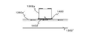
- FIG. 14A, FIG. 14B, and FIG. 14C show an example of a configuration for causing a part of light propagating through the branching waveguide 1360a to enter the photodetector 1362a, in the portion of the LN substrate 1302 on which the photodetector 1362a is mounted. It is the figure shown in the cross section along the branched waveguide 1360a.
- a photodetector 1362a is disposed on the branch waveguide 1360a, and the photodetector 1362a is bonded to the branch waveguide 1360a with a transparent resin 1400.
- a groove 1404 is formed on the surface portion of the LN substrate 1302 ′′ where the branching waveguide 1360a ′′ is formed, and light propagating through the branching waveguide 1360a ′′ is transmitted from the wall surface of the groove. The light is emitted, and the emitted light is incident on the photodetector 1362a and received.
- the frequency of the dither signal applied to the bias electrode 1358a or the like is selected to be a frequency that is lower than the high frequency signal applied to the RF electrode and does not affect the high frequency signal.
- dither signals having different frequencies are used for each bias electrode so that it is easy to determine which bias electrode the dither signal is applied to.
- the dither signal applied to each device electrode does not affect the RF signal frequency (usually several tens of GHz), the frequencies are not close to each other, and feedback control of the necessary speed can be performed.
- Etc. are selected in the range of several kHz to several hundred MHz.
- the conventional optical modulator having the above-described configuration can appropriately operate with a temperature drift and the like compensated well.
- an optical modulator using a plurality of bias electrodes for example, DP-QPSK modulator
- bias voltage control that has not been seen in an optical modulator having a single bias electrode. Can occur.
- This problem is characteristic of an optical modulator using a plurality of bias electrodes, and the following phenomenon has been observed. -When a dither signal is applied to one bias electrode, optical characteristic control (phase adjustment or temperature drift compensation) in one or more other bias electrodes may become unstable. In this case, the instability phenomenon may be observed at the one bias electrode in addition to the other bias electrodes.
- the instability phenomenon can occur not only between adjacent or close bias electrodes, but also between non-adjacent bias electrodes or close bias electrodes.
- the above unstable phenomenon may or may not occur depending on the ambient temperature around the optical modulator. •
- the above unstable phenomenon may be resolved by changing the dither signal frequency to another frequency. The above unstable phenomenon does not occur when only a DC voltage is applied to each bias electrode.
- the above instability phenomenon is a phenomenon that cannot be explained by “electrical interference generated between adjacent electrodes”, and its cause has not been understood for a long time.
- the inventor of the present invention has examined the above unstable phenomenon of the bias control operation in an optical modulator having a plurality of bias electrodes in detail, and as a result, the cause of the unstable phenomenon is that a dither signal is applied to the bias electrode on the LN substrate. It was found that surface acoustic waves (Surface Acoustic Wave: SAW) generated by application. That is, when a dither signal is applied to one bias electrode formed on the LN substrate, a surface acoustic wave (Surface Acoustic Wave: SAW) is generated on the surface of the substrate due to the piezoelectric effect of the substrate material LN.
- SAW Surface Acoustic Wave
- the other bias electrode When the surface acoustic wave propagates through the substrate surface and reaches the other bias electrode, the other bias electrode receives the dither signal applied to the one bias electrode, and the received dither signal is transmitted to the other bias electrode. This adversely affects the bias control operation of the bias electrode.
- This surface acoustic wave is a sound wave that propagates, reflects, and scatters on the surface of the substrate, and also acts on a bias electrode that is not close to the surface, and changes in physical properties of the substrate due to temperature changes ( The strength and frequency change due to the linear expansion of the substrate. For this reason, the instability phenomenon occurs even between bias electrodes that are not adjacent or not close to each other, and the instability phenomenon may or may not occur depending on the environmental temperature.
- the comb electrode since the comb electrode is used as the bias electrode, the efficiency when the electric signal applied to the comb electrode is converted into a surface acoustic wave (for example, the generated surface acoustic wave with respect to the power of the applied electric signal).
- a dither signal having a frequency equal to the characteristic frequency at which the electroacoustic conversion efficiency representing the power ratio is maximized is applied to the bias electrode, the instability phenomenon becomes significant. This characteristic frequency is determined by the electrode spacing of the comb-shaped electrodes that are bias electrodes.
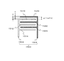
- FIG. 15 is a diagram illustrating an example of a configuration of a comb-shaped electrode that can be used as a bias electrode of an optical modulator.
- the illustrated comb-shaped electrode 1500 includes two electrodes 1502 and 1504.
- the electrodes 1502 and 1504 are three electrodes 1510, 1512, 1514, and 1520 and 1522 that extend in parallel to each other in the illustrated horizontal direction.
- 1524 (hereinafter, electrode portions of the comb-shaped electrodes such as the electrodes 1510, 1512, 1514 and 1520, 1522, 1524 which are parallel to each other are also referred to as “electrodes constituting the comb-shaped electrodes”).
- a total of six electrodes 1520, 1510, 1522, 1512, 1524, 1514 have the same electrode width h and are separated by a gap (electrode gap) a. Therefore, the electrode interval (pitch) p is given by the following equation (1).
- the characteristic frequency f 0 of the comb-shaped electrode 1500 (that is, the frequency at which the electroacoustic conversion efficiency is maximized) is given by the following equation (2).
- v is the propagation speed of the surface acoustic wave on the substrate surface
- ⁇ is the wavelength of the surface acoustic wave.
- the comb-shaped electrode having the electrode interval p has the characteristic frequency f 0 represented by the equation (2), and when a voltage signal having a frequency equal to the characteristic frequency f 0 is applied, the characteristic frequency f 0 is applied.
- the surface acoustic wave having a frequency equal to is strongly excited.
- the characteristic frequency f 0 can be changed by changing the electrode width h and / or the electrode gap a to change the electrode interval p.
- the surface acoustic wave propagation velocity v varies depending on the type of material used for the substrate, the direction of the substrate surface relative to the molecular arrangement of the material (for example, the crystal orientation), and the propagation direction of the surface acoustic wave.
- the surface acoustic wave propagating in the Z direction is about 3500 m / s
- the surface acoustic wave propagating in the X direction is used. Then, the propagation speed is about 4000m / s.
- the electrode width h and the electrode gap a are determined in consideration of the horizontal field pattern and field diameter (usually about 10 ⁇ m) of the light wave propagating through the optical waveguide.
- the characteristic frequency f 0 is about 50 MHz.
- a dither signal having a frequency component close to 50 MHz is applied to the bias electrode constituted by the illustrated comb electrode 1500, a strong surface acoustic wave is excited.
- This surface acoustic wave propagates on the substrate surface in a direction (vertical direction in the figure) perpendicular to the length direction of the electrode (for example, electrode 1520) constituting the comb-shaped electrode 1500, and another bias electrode (comb-shaped electrode) To reach.
- the surface acoustic wave is converted into an electric signal by the piezoelectric effect, and a noise signal having the above frequency is generated, which is influenced by the bias control operation.
- the degree of influence of the other bias electrode is such that the other bias electrode is disposed at a position where the surface acoustic wave arrives from a direction orthogonal to the length direction of the electrode constituting the other bias electrode, and It becomes strongest when it has the same characteristic frequency as that of the surface acoustic wave.
- the degree of the influence also depends on the value of the electroacoustic conversion efficiency at the characteristic frequency of the other device, and the greater the efficiency, the larger the effect.
- the inventor of the present invention devised a new configuration for suppressing or reducing interference between bias electrodes via surface acoustic waves, and the configuration is effective for suppressing the interference.
- the specific configuration is described in Japanese Patent Application No. 2016-036962).
- the optical modulator 1300 shown in FIG. 13 it is included in the optical signal modulated by the dither signal applied to the bias electrode 1358a or the like (more specifically, the outgoing light propagating through the outgoing waveguide 1322a).
- the photodetectors 1362a and 1362b for detecting the magnitude of the dither signal component are provided on the substrate 1302, as a further problem, the surface elasticity generated in the bias electrode 1358a and the like. Waves can propagate through the substrate surface of the LN substrate 1302 to reach the mounting area of the photodetectors 1362a, 1362b, causing fluctuations in the power of light received at the photodetectors 1362a, 1362b.
- the photodetectors 1362a and 1362b are arranged close to the upper portions of the branching waveguides 1360a and 1360b as shown in FIGS. 14A, 14B, and 14C, and therefore surface acoustic waves that propagate on the surface of the LN substrate 1302 .
- the geometric distance between the photodetectors 1362a, 1362b and the branch waveguides 1360a, 1360b will slightly vary. For this reason, the amount of light (received light amount) emitted from the branch waveguides 1360a and 1360b and received by the photodetectors 1362a and 1362b may vary due to the slight change in the geometric distance.
- the state of propagating light changes via a photoelastic effect (a phenomenon in which the refractive index changes when pressure is applied) and the like, and is received by the photodetectors 1362a and 1362b.
- the amount of light can vary.
- This variation in the received light quantity includes the frequency components of various surface acoustic waves that propagate (that is, the frequency components of the dither signal applied to the bias electrode 1358a and the like), and therefore the outgoing light (modulation) that propagates through the outgoing waveguide 1322a.
- a detection error is generated in the photodetectors 1362a and 1362b regarding the intensity of the dither signal component included in the light.
- bias voltage control operation also referred to as bias control operation
- the detection error of the dither signal component due to such surface acoustic waves in the photodetector formed on the same substrate as the bias electrode includes many bias electrodes as shown in FIG. It can be generated not only in an optical modulator that can generate surface acoustic waves, but also in an optical modulator having only a single bias electrode, and it may be necessary to reduce the detection error.
- an optical modulator comprising a bias electrode to which a bias voltage and a dither signal are applied and a photodetector for monitoring the intensity of a dither signal component included in the emitted light on the same substrate. It is desired to reduce the detection error of the dither signal component intensity detected by the detector and eliminate the unstable phenomenon of the bias control operation.
- the optical modulator includes a substrate having a piezoelectric effect, an optical waveguide formed on the substrate, a bias electrode for controlling a light wave propagating through the optical waveguide, and formed on the substrate and propagating through the optical waveguide.
- a light detector for monitoring a light signal to be detected, and the light detection from the bias electrode between a region on the substrate where the bias electrode is formed and a portion where the light detector is disposed.
- At least one suppression means for suppressing surface acoustic waves propagating to the vessel is arranged.
- the suppressing means is configured by a metal film provided between the region on the substrate where the bias electrode is formed and the portion where the photodetector is disposed. Is done.
- the metal film is an electrode to which the photodetector is connected.
- the suppression means is made of a resin applied between a region on the substrate where the bias electrode is formed and a portion where the photodetector is disposed.
- the suppression means is composed of a metal film formed on the substrate so as to surround the periphery of the photodetector.
- the suppression means is made of a resin coated on the substrate around the edge portion of the photodetector.
- the suppression means is made of a resin coated on the substrate so as to surround the periphery of the photodetector.
- Another aspect of the present invention is an optical transmission device including any one of the above optical modulators.
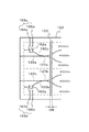
- FIG. 2 is a partial detail view of a periphery of a guard pattern, which is a surface acoustic wave suppressing unit, of the optical modulator shown in FIG. 1. It is a figure which shows the 1st modification of the surface acoustic wave suppression means which can be used for the optical modulator shown in FIG. It is a figure which shows the 2nd modification of the surface acoustic wave suppression means which can be used for the optical modulator shown in FIG. It is a figure which shows the 3rd modification of the surface acoustic wave suppression means which can be used for the optical modulator shown in FIG.
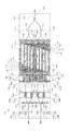
- FIG. 11 is a partial detail view of a periphery of a groove that is a surface acoustic wave suppressing unit of the optical modulator shown in FIG. 10. It is a figure which shows the structure of the optical transmitter which concerns on the 3rd Embodiment of this invention. It is a figure which shows the structure of the conventional optical modulator. It is a figure which shows an example of the structure for making a part of light which propagates a branched waveguide in an optical modulator enter into a photodetector.
- the optical modulator shown in the present embodiment is, for example, a DP-QPSK modulator.
- the present invention is not limited to this, and the bias electrode and light detection for monitoring (monitoring) emitted light (modulated light). Can be implemented by various types of light modulators provided on the same substrate.
- FIG. 1 is a diagram showing a configuration of an optical modulator according to the first embodiment of the present invention.
- the optical modulator 100 according to the present embodiment is, for example, a DP-QPSK modulator, and its basic configuration is the same as that of the conventional DP-QPSK modulator 1300 shown in FIG.
- the optical modulator 100 includes, for example, a nest type Mach-Zehnder optical waveguide (shown by a thick dotted line) formed on a Z-cut LN substrate 102 and an electrode (shown by a hatched portion).
- this optical modulator light from a light source (not shown) such as a laser diode is incident from the right in the figure, and the modulated light is emitted from the left in the figure.
- the emitted light is combined by, for example, a spatial optical system and is incident on an optical fiber connected to the optical transmission path.
- the optical waveguide modulates the incident waveguide 104 that receives incident light from the right direction in the figure, the optical branching unit 106 that branches the light propagating through the incident waveguide 104, and the light branched by the optical branching unit 106. And two Mach-Zehnder optical waveguides 110a and 110b.
- the Mach-Zehnder optical waveguide 110a includes an incident waveguide 112a, an optical branching portion 114a that branches light propagating through the incident waveguide 112a, and parallel waveguides 116a and 118a that propagate respective lights branched by the optical branching portion 114a. And a multiplexing unit 120a that combines the light propagated through the parallel waveguides 116a and 118a, and an output waveguide 122a that outputs the light combined by the multiplexing unit 120a to the outside.
- the Mach-Zehnder optical waveguide 110a includes Mach-Zehnder optical waveguides 130a (parts in a rectangle indicated by a dotted line in the figure) and 132a (parts in a rectangle indicated by a two-dot chain line in the figure) respectively formed in a part of the parallel waveguides 116a and 118a. ).
- Electrodes are respectively provided on the light exit sides (left side in the drawing) of the parallel waveguides 134a and 136a of the Mach-Zehnder optical waveguide 130a and on the light exit sides (left side in the drawing) of the parallel waveguides 138a and 140a of the Mach-Zehnder optical waveguide 132a.
- a bias electrode 146a composed of 142a and 144a and a bias electrode 152a composed of electrodes 148a and 150a are formed.
- a bias electrode 158a composed of electrodes 154a and 156a is formed on the light exit side (left side in the drawing) of the parallel waveguides 116a and 118a of the Mach-Zehnder optical waveguide 110a.
- Each bias electrode 146a, 152a, 158a, 146b, 152b, 158b constitutes a comb-shaped electrode as shown.
- the configuration of the Mach-Zehnder optical waveguide 110b is the same as that of the Mach-Zehnder optical waveguide 110a as shown in the figure.
- the optical modulator 100 includes electrodes 170 on the eight parallel waveguides 134a, 136a, 138a, 140a, 134b, 136b, 138b, and 140b of the four Mach-Zehnder optical waveguides 130a, 132a, 130b, and 132b, respectively.
- RF electrodes composed of 172, 174, 176, 178, 180, 182, 184, 186 are also formed.
- the bias electrodes 146a, 152a, 146b, and 152b are bias electrodes for adjusting the bias point of the optical modulator constituted by the Mach-Zehnder optical waveguides 130a, 132a, 130b, and 132b, respectively.
- Reference numeral 158b denotes a bias electrode for adjusting the phase of light emitted from the output waveguides 122a and 122b.
- the optical modulator 100 further includes branch waveguides 160a and 160b extending from the multiplexing sections 120a and 120b and branching part of the outgoing light propagating through the output waveguides 122a and 122b, respectively.
- photodetectors 162a and 162b disposed on the substrate surface of the LN substrate 102 on which the waveguides 160a and 160b are formed.
- the photodetectors 162a and 162b are configured by using, for example, a photodiode (PD, Photo Diode) as a light detection element (not shown), and light from the branching waveguides 160a and 160b is received by the light detection element.
- the photodetection element is arranged so as to face the branching waveguides 160a and 160b.
- the photodetectors 162a and 162b are fixed to the portion of the surface of the LN substrate 102 where the branching waveguides 160a and 160b are formed, for example, with an adhesive using a transparent resin. Similarly to the configuration shown, light (evanescent light) that has oozed out from the branching waveguides 160a and 160b is received.
- the outputs of the photodetectors 162a and 162b are output to the outside of the optical modulator 100 via a monitor electrode 168a composed of electrodes 164a and 166a and a monitor electrode 168b composed of electrodes 164b and 166b, respectively. .
- the optical modulator 100 of the present embodiment includes a region on the LN substrate 102 where the bias electrodes 146a, 152a, 146b, 152b, 158a, 158b having a comb-like electrode structure for generating surface acoustic waves are formed,
- a guard pattern 190 made of a metal film is formed on the LN substrate 102 between the portions (or regions) where the detectors 162a and 162b are arranged.
- This guard pattern 190 acts as an absorber of surface acoustic waves propagating on the surface of the LN substrate 102, and is generated from the bias electrodes 146a, 152a, 146b, 152b, 158a, 158b and on the mounting portions of the photodetectors 162a, 162b.
- Suppressing means (hereinafter also referred to as surface acoustic wave suppressing means) that suppresses (or prevents) the surface acoustic wave that arrives is configured.
- FIG. 2 is a partial detail view of the periphery of the guard pattern 190 of the optical modulator 100 shown in FIG.
- a surface acoustic wave (schematically indicated by a wavy arrow in the figure) coming from the region where the bias electrodes 146a, 152a, 146b, 152b, 158a, 158b are formed on the right side of the guard pattern 190 is absorbed by the guard pattern 190.
- the arrival of the photodetectors 162a and 162b at the mounting portion is prevented or suppressed.
- the guard pattern 190 includes a region where the bias electrodes 146a, 152a, 146b, 152b, 158a, 158b having a comb electrode structure for generating surface acoustic waves are formed, and a portion where the photodetectors 162a, 162b are disposed. As long as it is arranged between (or region), it can be provided at any position.
- the guard pattern 190 can be formed using, for example, gold (Au), and the surface acoustic wave absorption effect by the guard pattern 190 is an area where the bias electrodes 146a, 152a, 146b, 152b, 158a, 158b are formed.
- the width d20 of the guard pattern 190 measured along the direction toward the region where the photodetectors 162a and 162b are arranged is higher, and the guard pattern 190 is higher in thickness. Therefore, the size (including thickness) of the guard pattern 190 is preferably determined according to the intensity of the surface acoustic wave that can be generated from the bias electrodes 146a, 152a, 146b, 152b, 158a, 158b.
- the width d20 of the guard pattern 190 is preferably at least longer than the wavelength of the surface acoustic wave from the viewpoint of effectively absorbing the surface acoustic wave, and thus generated from the bias electrodes 146a, 152a, 146b, 152b, 158a, 158b. It is particularly desirable that the surface acoustic wave be wider than the longest wavelength ⁇ max (that is, d20 ⁇ ⁇ max).
- a metal film when a metal film is formed on an optical waveguide, it is known that light propagating through the optical waveguide is absorbed and attenuated by the metal film. Therefore, in order to prevent such light attenuation, for example, the light is refracted more than the optical waveguide (for example, 116a, 116b, etc.) formed on the LN substrate 102 between the guard pattern 190 and the surface of the LN substrate 102.
- a buffer layer using a low-rate material for example, SiO 2
- a guard pattern 190 shown in FIGS. 1 and 2 is removed by removing a portion formed on an optical waveguide (for example, 116a, 116b). 190 may be composed of a plurality of metal film portions.
- a region where the bias electrodes 146a, 152a, 146b, 152b, 158a, 158b that generate surface acoustic waves are formed, and a portion (region) where the photodetectors 162a, 162b are disposed,
- a guard pattern 190 made of a metal film that absorbs surface acoustic waves is provided as surface acoustic wave suppression means.
- surface acoustic wave suppression means can be used.
- FIGS. 3 to 9 show various surface acoustic wave suppressing means that can be used in place of the guard pattern 190.
- FIG. FIGS. 3 to 9 show the surface acoustic wave suppressing means that can be used in place of the guard pattern 190 by taking the peripheral portion of the photodetector 162a as an example, but the configurations shown in FIGS.
- the present invention can be similarly applied to the peripheral portion of the photodetector 162b to suppress or prevent the surface acoustic wave reaching the photodetector 162b.
- FIG. 3 is a diagram showing surface acoustic wave suppressing means that can be used in place of the guard pattern 190 according to this modification.
- the same components as those shown in FIGS. 1 and 2 are denoted by the same reference numerals as those shown in FIGS. 1 and 2, and the above-described description of FIGS. Shall be incorporated.
- regions where bias electrodes 146 a, 152 a, 146 b, 152 b, 158 a, 158 b having comb-shaped electrode structures for generating surface acoustic waves are formed on the LN substrate 102 as surface acoustic wave suppressing means. And a portion (region) where the photodetector 162a is disposed, a resin 390 is applied on the LN substrate 102.
- This resin 390 acts as a surface acoustic wave absorber that propagates on the surface of the LN substrate 102 and is generated from the bias electrodes 146a, 152a, 146b, 152b, 158a, 158b and reaches the mounting portion of the photodetector 162a.
- a surface acoustic wave suppressing means for suppressing or blocking the elastic wave is configured.
- the resin 390 can be, for example, an ultraviolet curable adhesive and / or an epoxy adhesive.
- the surface acoustic wave absorption effect by the resin 390 is along the direction from the region where the bias electrodes 146a, 152a, 146b, 152b, 158a, 158b are formed to the region where the photodetectors 162a, 162b are arranged.
- the width d30 of the resin 390 is desirably at least longer than the wavelength of the surface acoustic wave from the viewpoint of effectively absorbing the surface acoustic wave, and thus generated from the bias electrodes 146a, 152a, 146b, 152b, 158a, 158b. It is particularly desirable that the surface acoustic wave is wider than the longest wavelength ⁇ max (that is, d30 ⁇ ⁇ max).
- FIG. 4 is a diagram showing a surface acoustic wave suppressing unit that can be used in place of the guard pattern 190 according to this modification.
- the same components as those shown in FIGS. 1 and 2 are denoted by the same reference numerals as those shown in FIGS. 1 and 2, and the description of FIGS. Shall be incorporated.
- the mounting portion (or mounting region) of the photodetector 162a is surrounded with respect to the region where the bias electrode 146a and the like for generating surface acoustic waves are formed.
- a rectangular frame-shaped guard pattern 490 made of metal (for example, gold (Au)) that absorbs surface acoustic surface waves is formed on the LN substrate 102.
- the guard pattern 490 effectively suppresses or prevents surface acoustic waves that reach the photodetector 162a from the four sides of the photodetector 162a.
- the effect of suppressing (blocking) surface acoustic waves by the guard pattern 490 depends on the width d40 and the thickness of the band-shaped metal pattern constituting the guard pattern 490. As shown in FIG. 4, since the electrodes 164a, 166a and the like connected to the photodetector 162a are arranged close to each other in the vicinity of the photodetector 162a, if the width d40 cannot be secured sufficiently large, It is necessary to increase the thickness of the metal pattern.
- the width d40 of the band-shaped metal pattern constituting the guard pattern 490 is longer than at least the incoming surface acoustic wave, and accordingly, the bias electrodes 146a, 152a, and 146b. , 152b, 158a, 158b is particularly desirable to be wider than the longest wavelength ⁇ max of surface acoustic waves (that is, d40 ⁇ ⁇ max).
- FIG. 5 is a diagram showing surface acoustic wave suppressing means that can be used in place of the guard pattern 190 according to this modification.
- the same components as those shown in FIGS. 1 and 2 are denoted by the same reference numerals as those shown in FIGS. 1 and 2, and the above description of FIGS. 1 and 2 is performed. Shall be incorporated.
- the mounting portion (or mounting region) of the photodetector 162a is surrounded with respect to the region where the bias electrode 146a and the like for generating the surface acoustic wave are formed as the surface acoustic wave suppressing means.
- a resin 590 that absorbs surface acoustic wave is applied on the LN substrate 102.
- the resin 590 effectively suppresses or prevents surface acoustic waves that reach the photodetector 162a from the four sides of the photodetector 162a.
- Desirable conditions for the width and thickness of the resin 590 are the same as those of the resin 390 which is the first modification shown in FIG. 3, and in particular, d50 ⁇ ⁇ max ( ⁇ max is the longest wavelength of the surface acoustic wave that can be generated). It is desirable to be.
- FIG. 6 is a view showing a surface acoustic wave suppressing unit that can be used in place of the guard pattern 190 according to this modification.
- the same components as those shown in FIGS. 1 and 2 are denoted by the same reference numerals as those shown in FIGS. 1 and 2, and the above-described description of FIGS. Shall be incorporated.
- the electrodes 366a and 366b constituting the monitor electrode 368a connected to the photodetector 162a are formed in the region where the bias electrode 146a and the like for generating surface acoustic waves are formed and the light detection.
- the electrodes 162a and 366b function as surface acoustic wave suppression means.
- at least one of the widths d60 and d62 of the electrodes 366a and 366b can be generated from the bias electrodes 146a, 152a, 146b, 152b, 158a and 158b. It is particularly desirable to be wider than the longest wavelength ⁇ max of the wave.
- FIGS. 1 and 2 are diagrams showing surface acoustic wave suppressing means that can be used in place of the guard pattern 190 according to this modification.
- 7A and 7B the same components as those shown in FIGS. 1 and 2 are denoted by the same reference numerals as those shown in FIGS. 1 and 2, and the above-described FIGS. The explanation about is to be incorporated.
- FIG. 7A is a partial detail view around the photodetector 162a
- FIG. 7B is an AA cross-sectional view of the portion of the photodetector 162a.
- the description of the branching waveguide 160a is omitted.
- the edge of the photodetector 162a facing the region where the bias electrode 146a and the like for generating surface acoustic waves are formed (that is, the right side in the drawing)
- the resin 790 is applied over a length d70 from the edge (also referred to as “edge in the arrival direction of the surface acoustic wave”).
- the resin 790 functions as a surface acoustic wave suppressing unit, and suppresses surface acoustic waves that arrive at the photodetector 162a from the region where the bias electrode 146a and the like are formed.
- the coating length d70 of the resin 790 is the length from the edge of the surface acoustic wave arrival direction of the photodetector 162a to the end of the resin 790, and arrives from the viewpoint of effectively blocking the surface acoustic wave. It is desirable that the surface acoustic wave has the longest wavelength ⁇ max or more (that is, d70 ⁇ ⁇ max).
- the resin 790 may be, for example, an ultraviolet curable and / or epoxy adhesive, as in the resin 390 according to the first modification shown in FIG.
- this adhesive can use the same material as the adhesive that fixes the photodetector 162a on the substrate. In this case, an amount larger than the normal adhesive amount for fixing the photodetector 162a on the substrate is applied, and the adhesive protrudes around the edge portion of the photodetector at the time of fixing. In this way, it is possible to realize a configuration that suppresses the influence of surface acoustic waves without increasing the number of assembly steps, which is preferable.
- the resin is applied. This is because, for example, by applying an equal amount of resin to the opposite edge portion of the adhesive resin 790, these resin portions applied to the opposite edge portions thermally expand by substantially the same amount when the environmental temperature changes. This is to suppress the fluctuation due to the environmental temperature fluctuation of the optical coupling efficiency between the branching waveguide 160a and the photodetector 162a so as to contract.
- the resin 162 is applied to the edge of the surface acoustic wave arrival direction and the edge facing the edge of the photodetector 162a.
- Resin may be applied to the entire peripheral edge of the photodetector 162a.
- the distance of the resin-coated portion that spreads outward from the edge of the photodetector 162a is equal to or longer than the longest wavelength ⁇ max of the incoming surface acoustic waves, like the length d70. Thereby, the surface acoustic wave which arrives from the four directions toward the photodetector 162a can be effectively suppressed.
- FIG. 8 is a diagram showing surface acoustic wave suppressing means that can be used in place of the guard pattern 190 according to this modification.
- the same constituent elements as those shown in FIGS. 1 and 2 are denoted by the same reference numerals as those shown in FIGS. 1 and 2, and the description of FIGS. Shall be incorporated.
- This modification is a combination of a guard pattern 490 according to the second modification shown in FIG. 4 and a resin 790 according to the fifth modification shown in FIGS. 7A and 7B. That is, in this modification, as shown in FIG. 8, a rectangular frame guard pattern 890 made of a band-shaped metal film (for example, gold (Au)) having a width d80 so as to surround the mounting portion of the photodetector 162a. In addition, a resin 892 is applied over a distance d82 from the edge of the photodetector 162a on the side in the direction of the region where the bias electrode 146a and the like for generating surface acoustic waves are formed. ing.
- a rectangular frame guard pattern 890 made of a band-shaped metal film (for example, gold (Au)) having a width d80 so as to surround the mounting portion of the photodetector 162a.
- a resin 892 is applied over a distance d82 from the edge of the photodete
- the guard pattern 890 and the resin 892 function as surface acoustic wave suppressing means, and incoming surface acoustic waves can be more effectively blocked. From the viewpoint of effectively blocking surface acoustic waves, it is desirable that at least one of the width d80 and the distance d82 is not less than the longest wavelength ⁇ max of the incoming surface acoustic waves.
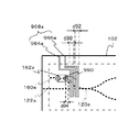
- FIG. 9 is a diagram showing surface acoustic wave suppressing means that can be used in place of the guard pattern 190 according to this modification. 9, the same components as those shown in FIGS. 1 and 2 are denoted by the same reference numerals as those shown in FIGS. 1 and 2, and the above-described description of FIGS. 1 and 2 is performed. Shall be incorporated.
- This modification is a combination of the monitor electrode 668a according to the fourth modification shown in FIG. 6 and the resin 790 according to the fifth modification shown in FIGS. 7A and 7B. That is, in this modification, as shown in FIG. 9, the electrodes 964a and 966a constituting the monitor electrode 968a connected to the photodetector 162a have the widths d90 and d92, respectively, and the bias electrode 146a that generates surface acoustic waves. Etc., and a portion (region) where the photodetector 162a is disposed.
- Resin 990 is applied over the length d94 from the edge. That is, in this modification, the electrodes 964a and 966a and the resin 990 function as surface acoustic wave suppression means, and more effectively suppress incoming surface acoustic waves.
- At least one of d90, d92, and d94 has the longest wavelength ⁇ max or more of the surface acoustic waves that arrive.
- the resin 990 is applied to the edge portion of the photodetector 162a in the arrival direction of the surface acoustic wave.
- the present invention is not limited to this.
- the end portions of the electrodes 964a and 966a (the lower portion in the drawing)
- the resin 990 may be applied to the lower edge portion of the photodetector 162a in order to further block the surface acoustic wave that wraps around from the end portion and arrives at the photodetector 162a.
- FIG. 10 is a diagram illustrating a configuration of an optical modulator according to the second embodiment of the present invention.
- the same reference numerals as those in FIG. 1 are used for the same components as those of the optical modulator 100 according to the first embodiment shown in FIG. 1, and the above description of the first embodiment is incorporated. It shall be.
- An optical modulator 1000 according to this embodiment shown in FIG. 10 has the same configuration as the optical modulator 100 according to the first embodiment, but includes an LN substrate 1002 instead of the LN substrate 102, and the LN substrate 1002 is Instead of the guard pattern 190, groove portions 1090a, 1090b, and 1090c (collectively referred to as groove portions 1090) are provided in the vicinity of the combining portions 120a and 120b.
- the groove 1090 includes regions where bias electrodes 146a, 152a, 146b, 152b, 158a, 158b having comb-like electrode structures for generating surface acoustic waves are formed, and a photodetector.
- the surface acoustic wave suppressing means in the optical modulator 1000 is configured between the region where the 162a and 162b are disposed.
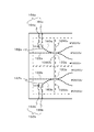
- FIG. 11 is a partial detail view around the groove 1090 of the optical modulator 1000 shown in FIG.
- Surface acoustic waves (schematically indicated by the wavy arrow shown) arriving from a region where the bias electrodes 146a, 152a, 146b, 152b, 158a, 158b are formed on the right side of the groove 1090 (that is, the grooves 1090a, 1090b, 1090c). ) Is prevented from propagating by the groove 1090, and the arrival of the photodetectors 162a and 162b at the mounting portion is suppressed.
- the groove 1090 is formed avoiding the optical waveguide forming portion on the LN substrate 1002, but the width of the optical waveguide is as narrow as about 10 ⁇ m, so the groove 1090 is formed avoiding the optical waveguide forming portion.
- the intensity of the surface acoustic wave that passes through the unexposed portions (that is, between the groove portions 1090a and 1090b and between the groove portions 1090b and 1090c) and reaches the photodetectors 162a and 162b is almost negligible.
- the groove 1090 includes a region where the bias electrodes 146a, 152a, 146b, 152b, 158a, 158b having a comb-like electrode structure for generating surface acoustic waves are formed, and a region where the photodetectors 162a, 162b are disposed. As long as it is between, it can be arranged at any position. However, as described above, the groove portion 1090 needs to be formed so as to avoid the portion where the optical waveguide is formed. Therefore, it is desirable that the groove portion 1090 be arranged so that the number of portions divided by the optical waveguide formation portion is reduced. For example, in the example shown in FIG.
- the groove portion 1090 is arranged at a position where only the multiplexing portions 120a and 120b need only be avoided (that is, four optical waveguides at positions shifted from the corresponding positions in the horizontal direction in the drawing). Whereas (116a, 118a, 116b, 118b, or 160a, 122a, 122b, 160b) are divided at the formation portion (that is, four locations), the portion is divided at the position of the groove 1090 shown in FIG. Will be two places).
- the present embodiment is an optical transmission device on which any one of the optical modulators 100 (including any modifications shown in FIGS. 3 to 9) and 1000 shown in the first and second embodiments is mounted.
- FIG. 12 is a diagram showing a configuration of the optical transmission apparatus according to the present embodiment.
- the optical transmitter 1200 includes an optical modulation unit 1220 including an optical modulator 1210, a light source 1230 that makes light incident on the optical modulator 1210, and an optical fiber 1240 that transmits light output from the optical modulation unit 1220.
- an optical modulation unit 1220 including an optical modulator 1210, a light source 1230 that makes light incident on the optical modulator 1210, and an optical fiber 1240 that transmits light output from the optical modulation unit 1220.
- the optical modulation unit 1220 also includes optical splitters 1250 and 1252 that split a part of two orthogonally two-polarized lights output from the optical modulator 1210, and one light split by the optical splitters 1250 and 1252, respectively.
- Receivers 1260 and 1262 respectively.
- the outputs of the light receivers 1260 and 1262 are output as feedback signals to a bias controller 1280 (described later).
- the light modulation unit 1220 includes a polarization beam combiner 1270.
- the optical modulator 1210 included in the optical modulation unit 1220 is one of the optical modulators 100 (including any modifications shown in FIGS. 3 to 9) and 1000 shown in FIGS.
- the optical unit 1270 combines the two orthogonally two-polarized lights output from the optical modulator 1210 and passed through the optical splitters 1250 and 1252, and inputs them to the optical fiber 1240.
- the optical transmission device 1200 also includes a bias control unit 1280 that is a control device that controls a bias electrode included in the optical modulator 1210.
- the bias controller 1280 applies a bias voltage obtained by superimposing a dither signal for detecting a change in the bias point to a DC voltage for bias point control to the bias electrode provided in the optical modulator 1210.
- the bias controller 1280 monitors the intensity of the dither signal frequency component in the feedback signal output from the light receivers 1260 and 1262 in the light modulation unit 1220, and applies it to the bias electrode provided in the light modulator 1210. The magnitude of the DC voltage is controlled.
- the bias controller 1280 applies a bias voltage using a dither signal having a different frequency for each bias electrode to each bias electrode.
- the dither signal is not limited to a sine wave, and can be a signal having an arbitrary waveform such as a sawtooth wave, a pulse wave, a triangular wave, and a staircase wave.
- the dither signal is not necessarily a signal that is always applied, and may be an electric signal that is intermittently applied for the purpose of detecting a bias point.
- the configuration in which the photodetector is installed on one of the two branched waveguides is illustrated. However, it is sufficient that the photodetector is configured on the substrate, and the number of branches of the waveguide is increased. Irrelevant and a photodetector may be installed in a portion not on the waveguide.
- the optical modulators (100, 1000) shown in the above-described embodiments are a plurality of bias electrodes (158a, etc.) and a photodetector (162a) for monitoring the intensity of emitted light (modulated light). Etc.) on the same substrate (102, etc.), and is generated from the bias electrode between the region where the bias electrode is formed and the portion where the photodetector is arranged on the substrate, to the photodetector.
- Surface acoustic wave suppression means (190 etc.) for suppressing the surface acoustic wave to reach is provided.
- the intensity of the emitted light detected by the photodetector 162a or the like is changed to the surface acoustic wave generated from the bias electrode 158a or the like by the dither signal applied to the bias electrode 158a or the like.
- the dither signal component intensity included in the emitted light can be accurately detected using the photodetector 162a or the like, so that a stable bias control operation can be performed, and the optical modulators 100 and 1000 can be The transmission quality of the used optical signal transmission can be maintained well.
Landscapes
- Physics & Mathematics (AREA)
- Nonlinear Science (AREA)
- General Physics & Mathematics (AREA)
- Optics & Photonics (AREA)
- Optical Modulation, Optical Deflection, Nonlinear Optics, Optical Demodulation, Optical Logic Elements (AREA)
Abstract
ディザ信号が印加されるバイアス電極と、光導波路内を伝搬する光信号を監視する光検出器と、を同一基板上に備える光変調器において、当該光検出器により検出されるディザ信号成分強度の検知精度を向上して、安定なバイアス制御を行う。本光変調器は、圧電効果を有する基板(102)と、当該基板上に形成された光導波路(116a等)と、当該光導波路を伝搬する光波を制御するバイアス電極(158a等)と、前記基板上に形成され、前記光導波路を伝搬する光信号を監視する光検出器(168a等)と、を備え、前記基板上の、前記バイアス電極が形成された領域と、前記光検出器が配された部分との間に、前記バイアス電極から前記光検出器へ伝播する表面弾性波を抑制する少なくとも一つの抑制手段(190等)が配されている。
Description
本発明は、光変調器、及び光変調器を用いた光送信装置に関し、特にバイアス電極と、出射光を監視する光検出器と、を同一基板上に形成した光変調器、及びそのような光変調器を用いた光送信装置に関する。
高速/大容量光ファイバ通信システムにおいては、導波路型の光変調器を組み込んだ光送信装置が多く用いられている。中でも、電気光学効果を有するLiNbO3(以下、LNともいう)を基板に用いた光変調器は、インジウムリン(InP)、シリコン(Si)、あるいはガリウム砒素(GaAs)などの半導体系材料を用いた変調器に比べて、光の損失が少なく且つ広帯域な光変調特性を実現し得ることから、高速/大容量光ファイバ通信システムに広く用いられている。
このLNを用いた光変調器では、マッハツェンダ光導波路と、変調信号である高周波信号を光導波路に印加するためのRF電極部と、当該光変調器における変調特性を良好に保つため種々の調整を行うためのバイアス電極と、が形成されている。このようなバイアス電極として、例えば、環境の温度変化等に起因するバイアス点の変動(いわゆる温度ドリフト現象)を補償すべく光導波路に電界を印加するためのバイアス電極や、光位相調整を行うためのバイアス電極がある。
一方、光ファイバ通信システムにおける変調方式は、近年の伝送容量の増大化の流れを受け、QPSK(Quadrature Phase Shift Keying)やDP-QPSK(Dual Polarization - Quadrature Phase Shift Keying)等、多値変調や、多値変調に偏波多重を取り入れた伝送フォーマットが主流となっている。
QPSK変調を行う光変調器(QPSK変調器)やDP-QPSK変調を行う光変調器(DP-QPSK変調器)は、ネスト型の複数のマッハツェンダ光導波路を備え、複数の高周波信号電極及び複数のバイアス電極を備えることから(例えば、特許文献1参照)、デバイスサイズが大型化する傾向があり、特に小型化の要請が強い。
従来、このような小型化のための技術として、各電極と光導波路との間の相互作用を高めて、長さの短い電極でも駆動電圧を低減することのできる方法が提案されている。例えば、各導波路に対し、バイアス電極をプッシュ用電極とプル用電極とで構成される櫛形電極(又は、すだれ状電極)として構成し、バイアス電極に印加すべき電圧(バイアス電圧)を低減する構成が知られている(例えば、特許文献2参照)。
図13は、従来のDP-QPSK変調器の構成の一例を示す図である。このDP-QPSK変調器1300は、例えばZカットのLN基板1302上に形成されたネスト型のマッハツェンダ光導波路(図示太線の点線)と、電極(図示ハッチング部分)とで構成されている。この光変調器では、レーザダイオード等の光源(不図示)からの光が図示右方向から入射し、変調された光が図示左方向から出射する。出射した光は、例えば空間光学系により合波されて、光伝送路につながった光ファイバに入射される。
光導波路は、図示右方向からの入射光を受ける入射導波路1304と、当該入射導波路を伝搬する光を分岐する光分岐部1306と、光分岐部1306で分岐されたそれぞれの光を変調する2つのマッハツェンダ光導波路部1310a、1310b、で構成されている。
マッハツェンダ光導波路部1310aは、入射導波路1312aと、当該入射導波路1312aを伝搬する光を分岐する光分岐部1314aと、光分岐部1314aで分岐されたそれぞれの光を伝搬させる平行導波路1316a、1318aと、当該平行導波路1316a、1318aを伝搬した光を合波する合波部1320aと、当該合波部1320aで合波された光を外部へ出射する出射導波路1322aと、を有する。また、マッハツェンダ光導波路部1310aは、上記平行導波路1316a及び1318aの一部にそれぞれ形成されたマッハツェンダ光導波路1330a(図示点線で示す矩形内の部分)、1332a(図示2点鎖線で示す矩形内の部分)を有する。
マッハツェンダ光導波路1330aの平行導波路1334a、1336aの光出射側(図示左方)と、マッハツェンダ光導波路1332aの平行導波路1338a、1340aの光出射側(図示左方)と、には、それぞれ、電極1342a、1344aで構成されるバイアス電極1346aと、電極1348a、1350aで構成されるバイアス電極1352aが形成されている。また、マッハツェンダ光導波路部1310aの平行導波路1316a、1318aの光出射側(図示左方)には、電極1354a、1356aで構成されるバイアス電極1358aが形成されている。
マッハツェンダ光導波路部1310bの構成は、図示のとおり、マッハツェンダ光導波路部1310aの構成と同様である。これにより、光変調器1300は、符号1346a、1352a、1358a、1346b、1352b、1358bで示される6個のバイアス電極を備える。また、光変調器1300には、4つのマッハツェンダ光導波路1330a、1332a、1330b、1332bの8本の平行導波路1334a、1336a、1338a、1340a、1334b、1336b、1338b、1340b上に、それぞれ電極1370、1372、1374、1376、1378、1380、1382、1384、1386で構成されるRF電極も形成されている。
ここで、バイアス電極1346a、1352a、1346b、1352bは、それぞれ、マッハツェンダ光導波路1330a、1332a、1330b、1332bで構成された光変調器のバイアス点を調整するためのバイアス電極であり、バイアス電極1358a及び1358bは、それぞれ、出射導波路1322a及び1322bから出射される光の位相を調整するためのバイアス電極である。
また、光変調器1300では、バイアス点調整や位相調整のために各バイアス電極1346a、1352a、1358a、1346b、1352b、1358bに印加すべき電圧を低減すべく、これらのバイアス電極が、図示のように櫛形電極として構成されている。
ところで、光変調器を実用装置に組み込んで使用する際には、上記温度ドリフトを補償して光伝送特性を良好な状態に維持すべく、バイアス点の変動が生じないようにバイアス電圧を正確に制御する必要がある。このため、温度ドリフトを補償するためのバイアス電極には、バイアス点の変化を検出するための低周波信号(ディザ信号)と、当該変化を補償してバイアス点を所定値に戻すための直流電圧(DCバイアス電圧)と、が印加される。
すなわち、ディザ信号をバイアス電極に印加しつつ、光変調器から出力される光信号を光検出器によりモニタし、当該光信号に含まれる当該ディザ信号の強度が最小となるように当該バイアス電極に印加するDCバイアス電圧を調整することで、温度ドリフト等のバイアス点の変化が補償される。
このようなDCバイアス電圧の制御のための光検出器は、例えば、図13に示すように、出射導波路1322a、1322bを伝搬する出射光(変調光)の一部を分岐する分岐導波路1360a、1360bの一部(すなわち、分岐導波路1360a、1360bが形成されたLN基板1302の表面の一部)にそれぞれ配された光検出器1362a、1362bとして実現され得る。光検出器1362a及び1362bの出力は、それぞれ、電極1364a、1366aで構成されるモニタ電極1368a、及び電極1364b、1366bで構成されるモニタ電極1368b、を介して光変調器1300の外部へ出力される。
図14A、図14B、図14Cは、分岐導波路1360aを伝搬する光の一部を光検出器1362aに入射させるための構成の例を、光検出器1362aが実装されたLN基板1302の部分の、分岐導波路1360aに沿った断面で示した図である。図14Aに示す構成では、分岐導波路1360a上に光検出器1362aが配され、光検出器1362aは分岐導波路1360aに対し透明樹脂1400により接着されている。この構成においては、分岐導波路1360aからしみだした光(エバネッセント光)を、光検出器1362aの図示下部エッジ付近に配された受光器(不図示)により入射させて受信している。また、図14Bに示す構成では、分岐導波路1360a´上部のLN基板1302´の表面に凹凸部1402を設けて表面粗さを粗くし、分岐導波路1360a´を伝搬する光を当該表面において散乱させて基板外に放射させ、当該放射させた光を光検出器1362aに入射させて受信している。また、図14Cに示す構成では、分岐導波路1360a´´が形成されたLN基板1302´´の表面部分に溝1404を形成し、分岐導波路1360a´´を伝搬する光を当該溝の壁面から出射させ、当該出射させた光を光検出器1362aに入射させて受信している。
バイアス電極1358a等に印加する上記ディザ信号の周波数は、特に、RF電極に印加される高周波信号よりも低い周波数であって、当該高周波信号に影響が出ないような周波数が選択される。また、バイアス電極が複数使用されている場合には、どのバイアス電極に印加されたディザ信号かを判別しやすいように、バイアス電極毎に異なる周波数のディザ信号が用いられる。
この場合、各デバイス電極に印加さるディザ信号は、RF信号周波数(通常は数十GHz)に影響を与えないこと、互いの周波数が近接していないこと、必要な速度のフィードバック制御を行い得ること、等を考慮して数kHzから数百MHzの範囲で選択される。
上記の構成を有する従来の光変調器は、一般には、温度ドリフト等が良好に補償されて適切に動作し得る。しかしながら、上記のように複数のバイアス電極を使用する光変調器(例えばDP-QPSK変調器)では、単一のバイアス電極を備える光変調器では見られなかったバイアス電圧制御についての新たな問題が発生し得る。この問題は、複数のバイアス電極を用いる光変調器に特徴的であり、以下のような現象が観測されている。
・一のバイアス電極にディザ信号を印加すると、一つ又は複数の他のバイアス電極における光特性制御(位相調整や温度ドリフト補償)が不安定になる場合がある。この場合、他のバイアス電極に加えて、当該一のバイアス電極でも上記不安定現象が観測される場合がある。
・上記不安定現象は、隣り合った又は接近したバイアス電極間だけでなく、隣り合っていないバイアス電極間や、接近していないバイアス電極間においても発生し得る。
・上記不安定現象は、光変調器の周囲の環境温度に依存して発生したりしなかったりすることがある。
・上記不安定現象は、ディザ信号の周波数を別の周波数に変更すると解消される場合がある。
・上記不安定現象は、各バイアス電極にDC電圧のみを印加した場合には発生しない。
・一のバイアス電極にディザ信号を印加すると、一つ又は複数の他のバイアス電極における光特性制御(位相調整や温度ドリフト補償)が不安定になる場合がある。この場合、他のバイアス電極に加えて、当該一のバイアス電極でも上記不安定現象が観測される場合がある。
・上記不安定現象は、隣り合った又は接近したバイアス電極間だけでなく、隣り合っていないバイアス電極間や、接近していないバイアス電極間においても発生し得る。
・上記不安定現象は、光変調器の周囲の環境温度に依存して発生したりしなかったりすることがある。
・上記不安定現象は、ディザ信号の周波数を別の周波数に変更すると解消される場合がある。
・上記不安定現象は、各バイアス電極にDC電圧のみを印加した場合には発生しない。
上記の不安定現象は、「近接した電極間で発生する電気的な干渉」では説明できない現象であって、長らくその要因は分かっていなかった。
本願発明の発明者は、複数のバイアス電極を備える光変調器におけるバイアス制御動作の上記不安定現象を詳細に検討した結果、当該不安定現象の原因が、LN基板上のバイアス電極にディザ信号が印加されることにより発生する表面弾性波(Surface Acoustic Wave : SAW)である、との知見を得た。すなわち、LN基板上に形成された一のバイアス電極にディザ信号が印加されると、基板素材であるLNが有する圧電効果により基板表面に表面弾性波(Surface Acoustic Wave : SAW)が発生し、当該表面弾性波が基板表面を伝搬して他のバイアス電極に達することで、当該他のバイアス電極が上記一のバイアス電極に印加されたディザ信号を受信し、当該受信されたディザ信号が当該他のバイアス電極におけるバイアス制御動作に干渉を与えて悪影響を及ぼすのである。
この表面弾性波は、基板表面を伝搬、反射、散乱する音波であって、近接しない離れたバイアス電極にも作用し、また温度変化による基板物性変化(特に、基板表面における音波の伝搬速度や、基板の線膨張)等によって、その強度や周波数が変化する。このため、隣り合っていない又は接近していないバイアス電極間でも上記不安定現象が生じ、また、環境温度に依存して上記不安定現象が発生したりしなかったりするのである。
また、バイアス電極として櫛形電極を用いているため、櫛形電極に印加された電気信号が表面弾性波に変換される際の効率(例えば、印加された電気信号のパワーに対する、発生する表面弾性波のパワーの比)を表す電気音響変換効率が最大となる特性周波数に等しい周波数のディザ信号が当該バイアス電極に印加されたときに、上記不安定現象が顕著となる。そして、この特性周波数は、バイアス電極である櫛形電極の電極間隔により定まる。
図15は、光変調器のバイアス電極に用いられ得る櫛形電極の構成の一例を示す図である。図示の櫛形電極1500は、2つの電極1502と1504とで構成され、電極1502、1504は、それぞれ、図示水平方向に互いに並行に延在する3本の電極1510、1512、1514、及び1520、1522、1524を有している(以下、電極1510、1512、1514、及び1520、1522、1524のような、櫛形電極が有する互いに並行な電極部分を、「櫛形電極を構成する電極」ともいう)。総計6本の電極1520、1510、1522、1512、1524、1514は、同じ電極幅hを持ち、間隙(電極間隙)aで隔てられている。従って、電極間隔(ピッチ)pは、次式(1)で与えられる。

このとき、櫛形電極1500の特性周波数f0(すなわち、電気音響変換効率が最大となる周波数)は、次の式(2)で与えられる。

ここで、vは、基板表面における表面弾性波の伝搬速度、λは、表面弾性波の波長である。換言すれば、電極間隔pを有する櫛形電極は、式(2)で示される特性周波数f0を持ち、当該特性周波数f0に等しい周波数を持つ電圧信号が印加されると、当該特性周波数f0に等しい周波数の表面弾性波を強く励振する。逆に、特性周波数f0を持つ櫛形電極に当該特性周波数f0に等しい周波数の表面弾性波が入射すると、当該櫛形電極には当該特性周波数f0に等しい周波数を持つ電気信号が強く誘導される。櫛形電極構造を有するバイアス電極では、当該誘導された電気信号が強い雑音信号となってバイアス制御動作に悪影響を与える。
式(2)から明らかなように、特性周波数f0は、電極幅h及び又は電極間隙aを変更して電極間隔pを変えることにより変化させることができる。
弾性表面波の伝搬速度vは、基板に用いた材料の種類や、当該材料の分子配列(例えば結晶方位)に対する基板表面の方向、及び弾性表面波の伝搬方向、等に依存して異なる値を持つ。例えば、基板としてYカットのLN基板を用いた場合、Z方向に伝搬する弾性表面波では3500m/s程度、基板として128°YカットのLN基板を用いた場合、X方向に伝搬する弾性表面波では4000m/s程度の伝搬速度となる。
電極幅hと電極間隙aとは、光導波路を伝搬する光波の横方向のフィールドパターンやフィールド径(通常約10μm程度)を考慮して定められる。
例えば、電極間隔15μm、電極幅20μm、表面弾性波の速度が3500m/sの場合、特性周波数f0は50MHz程度となる。この場合、図示の櫛形電極1500で構成されたバイアス電極に50MHzに近い周波数成分を持ったディザ信号が印加されると、強い表面弾性波が励振される。この表面弾性波は、当該櫛形電極1500を構成する電極(例えば電極1520)の長さ方向に対し直交する方向(図示上下方向)へ向かって基板表面を伝搬し、他のバイアス電極(櫛形電極)に達する。当該他のバイアス電極では、圧電効果によって当該表面弾性波が電気信号に変換され、上記周波数の雑音信号が生じて、バイアス制御動作に影響を受ける。
他のバイアス電極が受ける影響の程度は、当該他のバイアス電極が、当該他のバイアス電極を構成する電極の長さ方向に対し直交する方向から上記弾性表面波が到来する位置に配され、且つ当該弾性表面波の周波数と同じ特性周波数を持っている場合に、最も強くなる。また、当該影響の程度は、当該他のデバイスの当該特性周波数における電気音響変換効率の値にも依存し、当該効率が大きいほど大きい。
本願発明の発明者は、上記知見に基づき、表面弾性波を介したバイアス電極間の干渉を抑制又は低減するための新規な構成を考案し、当該構成が当該干渉の抑制に効果的であることを検証した(具体的構成については、特願2016-036962に記載されている)。
しかしながら、図13に示す光変調器1300のように、バイアス電極1358a等に印加されたディザ信号により変調された光信号(より具体的には、出射導波路1322aを伝搬する出射光)に含まれる当該ディザ信号成分の大きさを検知するための(バイアス点検出のための)光検出器1362a、1362bを基板1302上に設けた場合には、さらなる問題として、バイアス電極1358a等において発生した表面弾性波が、LN基板1302の基板表面を伝搬して光検出器1362a、1362bの実装領域まで達し、光検出器1362a、1362bにおいて受信される光のパワーに変動を生じさせ得る。
すなわち、光検出器1362a、1362bは、図14A、図14B、図14Cに示すように分岐導波路1360a、1360bの上部に近接して配置されるため、LN基板1302の表面を伝搬する表面弾性波が到来すると、光検出器1362a、1362bと分岐導波路1360a、1360bとの間の幾何学距離が僅かに変動することなる。このため、当該僅かな幾何学距離の変動によって、分岐導波路1360a、1360bから出射して光検出器1362a、1362bにより受信される光の量(受信光量)が変動することとなり得る。
また、光導波路に対し表面弾性波が作用すると、光弾性効果(圧力がかかると屈折率が変化する現象)等を介して伝搬光の状態が変化し、光検出器1362a、1362bにより受信される光の量が変動することとなり得る。
この受信光量の変動は、伝搬する種々の表面弾性波の周波数成分(すなわち、バイアス電極1358a等に印加されたディザ信号の周波数成分)を含み、したがって、出射導波路1322aを伝搬する出射光(変調光)に含まれるディザ信号成分の強度についての、光検出器1362a、1362bにおける検知誤差を生じさせる。その結果、光検出器1362a、1362bを用いて行われるバイアス電圧制御動作(バイアス制御動作ともいう)に不安定現象が生じ、光変調器1300によって変調される光の伝送品質が悪化することとなる。
そして、バイアス電極と同一の基板上に形成された光検出器における、このような表面弾性波に起因するディザ信号成分の検知誤差は、図13に示すような複数のバイアス電極を含んで多くの表面弾性波を生じ得る光変調器において発生し得るのみならず、単一のバイアス電極のみを有する光変調器においても発生し得るものであり、当該検知誤差の低減を講じることが必要となり得る。
上記背景より、バイアス電圧とディザ信号とが印加されるバイアス電極と、出射光に含まれるディザ信号成分の強度をモニタする光検出器と、を同一基板上に備える光変調器において、当該光検出器により検出されるディザ信号成分強度の検知誤差を低減して、バイアス制御動作の不安定現象を解消することが望まれている。
本発明の一の態様は、光変調器である。本光変調器は、圧電効果を有する基板と、当該基板上に形成された光導波路と、当該光導波路を伝搬する光波を制御するバイアス電極と、前記基板上に形成され、前記光導波路を伝搬する光信号を監視する光検出器と、を備え、前記基板上の、前記バイアス電極が形成された領域と、前記光検出器が配された部分との間に、前記バイアス電極から前記光検出器へ伝搬する表面弾性波を抑制する少なくとも一つの抑制手段が配されている。
本発明の他の態様によると、前記抑制手段は、前記基板上の、前記バイアス電極が形成された領域と、前記光検出器が配された部分と、の間に設けられた金属膜で構成される。
本発明の他の態様によると、前記金属膜は、前記光検出器が接続される電極である。
本発明の他の態様によると、前記抑制手段は、前記基板上の、前記バイアス電極が形成された領域と、前記光検出器が配された部分と、の間に塗布された樹脂で構成される。
本発明の他の態様によると、前記抑制手段は、前記光検出器の周囲を囲むように前記基板上に形成された金属膜で構成される。
本発明の他の態様によると、前記抑制手段は、前記光検出器のエッジ部周辺の前記基板上に塗布された樹脂で構成される。
本発明の他の態様によると、前記抑制手段は、前記光検出器の周囲を囲むように前記基板上に塗布された樹脂で構成される。
本発明の他の態様は、上記いずれかの光変調器を備える光送信装置である。
本発明の他の態様によると、前記抑制手段は、前記基板上の、前記バイアス電極が形成された領域と、前記光検出器が配された部分と、の間に設けられた金属膜で構成される。
本発明の他の態様によると、前記金属膜は、前記光検出器が接続される電極である。
本発明の他の態様によると、前記抑制手段は、前記基板上の、前記バイアス電極が形成された領域と、前記光検出器が配された部分と、の間に塗布された樹脂で構成される。
本発明の他の態様によると、前記抑制手段は、前記光検出器の周囲を囲むように前記基板上に形成された金属膜で構成される。
本発明の他の態様によると、前記抑制手段は、前記光検出器のエッジ部周辺の前記基板上に塗布された樹脂で構成される。
本発明の他の態様によると、前記抑制手段は、前記光検出器の周囲を囲むように前記基板上に塗布された樹脂で構成される。
本発明の他の態様は、上記いずれかの光変調器を備える光送信装置である。
以下、図面を参照して、本発明の実施の形態を説明する。なお、本実施形態に示す光変調器は、例えばDP-QPSK変調器であるが、本発明は、これに限らず、バイアス電極と、出射光(変調光)をモニタする(監視する)光検出器と、を同一基板上に備える種々のタイプの光変調器により実施することができる。
<第1実施形態>
まず、本発明の第1の実施形態について説明する。図1は、本発明の第1の実施形態に係る光変調器の構成を示す図である。上述したように、本実施形態に係る光変調器100は、例えばDP-QPSK変調器であり、その基本構成は図13に示す従来のDP-QPSK変調器1300と同様である。すなわち、本光変調器100は、例えばZカットのLN基板102上に形成されたネスト型のマッハツェンダ光導波路(図示太線の点線)と、電極(図示ハッチング部分)とで構成されている。この光変調器では、レーザダイオード等の光源(不図示)からの光が図示右方向から入射し、変調された光が図示左方向から出射する。出射した光は、例えば空間光学系により合波されて、光伝送路につながった光ファイバに入射される。
まず、本発明の第1の実施形態について説明する。図1は、本発明の第1の実施形態に係る光変調器の構成を示す図である。上述したように、本実施形態に係る光変調器100は、例えばDP-QPSK変調器であり、その基本構成は図13に示す従来のDP-QPSK変調器1300と同様である。すなわち、本光変調器100は、例えばZカットのLN基板102上に形成されたネスト型のマッハツェンダ光導波路(図示太線の点線)と、電極(図示ハッチング部分)とで構成されている。この光変調器では、レーザダイオード等の光源(不図示)からの光が図示右方向から入射し、変調された光が図示左方向から出射する。出射した光は、例えば空間光学系により合波されて、光伝送路につながった光ファイバに入射される。
光導波路は、図示右方向からの入射光を受ける入射導波路104と、当該入射導波路104を伝搬する光を分岐する光分岐部106と、光分岐部106で分岐されたそれぞれの光を変調する2つのマッハツェンダ光導波路110a、110bと、で構成されている。
マッハツェンダ光導波路110aは、入射導波路112aと、当該入射導波路112aを伝搬する光を分岐する光分岐部114aと、光分岐部114aで分岐されたそれぞれの光を伝搬させる平行導波路116a、118aと、当該平行導波路116a、118aを伝搬した光を合波する合波部120aと、当該合波部120aで合波された光を外部へ出射する出射導波路122aと、を有する。また、マッハツェンダ光導波路110aは、上記平行導波路116a及び118aの一部にそれぞれ形成されたマッハツェンダ光導波路130a(図示点線で示す矩形内の部分)、132a(図示2点鎖線で示す矩形内の部分)を有する。
マッハツェンダ光導波路130aの平行導波路134a、136aの光出射側(図示左方)と、マッハツェンダ光導波路132aの平行導波路138a、140aの光出射側(図示左方)と、には、それぞれ、電極142a、144aで構成されるバイアス電極146aと、電極148a、150aで構成されるバイアス電極152aが形成されている。また、マッハツェンダ光導波路110aの平行導波路116a、118aの光出射側(図示左方)には、電極154a、156aで構成されるバイアス電極158aが形成されている。そして、各バイアス電極146a、152a、158a、146b、152b、158bは、それぞれ、図示のように櫛形電極を構成している。
マッハツェンダ光導波路110bの構成は、図示のとおり、マッハツェンダ光導波路110aの構成と同様である。また、光変調器100には、4つのマッハツェンダ光導波路130a、132a、130b、132bの8本の平行導波路134a、136a、138a、140a、134b、136b、138b、140b上に、それぞれ電極170、172、174、176、178、180、182、184、186で構成されるRF電極も形成されている。
ここで、バイアス電極146a、152a、146b、152bは、それぞれ、マッハツェンダ光導波路130a、132a、130b、132bで構成された光変調器のバイアス点を調整するためのバイアス電極であり、バイアス電極158a及び158bは、それぞれ、出射導波路122a及び122bから出射される光の位相を調整するためのバイアス電極である。
また、光変調器100は、さらに、合波部120a、120bからそれぞれ延在して出射導波路122a、122bを伝搬する出射光の一部をそれぞれ分岐する分岐導波路160a、160bと、分岐導波路160a、160bが形成されたLN基板102の基板面上に配された光検出器162a、162bと、を備える。ここで、光検出器162a、162bは、例えばホトダイオード(PD、Photo Diode)を光検出素子(不図示)として用いて構成されており、当該光検出素子により分岐導波路160a、160bからの光をそれぞれ検出すべく、当該光検出素子が分岐導波路160a、160bと対面する位置となるように配されている。
また、光検出器162a、162bは、LN基板102の基板表面の、分岐導波路160a、160bが形成された部分に対し、例えば透明樹脂を用いた接着剤により固定されており、例えば図14Aに示す構成と同様に、それぞれ分岐導波路160a、160bからしみだした光(エバネッセント光)を受信する。
光検出器162a及び162bの出力は、それぞれ、電極164a、166aで構成されるモニタ電極168a、及び電極164b、166bで構成されるモニタ電極168b、を介して光変調器100の外部へ出力される。
特に、本実施形態の光変調器100は、LN基板102上の、表面弾性波を発生する櫛形電極構造を有するバイアス電極146a、152a、146b、152b、158a、158bが形成された領域と、光検出器162a、162bが配されている部分(又は領域)と、の間に、金属膜で構成されるガードパターン190がLN基板102上に形成されている。このガードパターン190は、LN基板102の表面を伝搬する表面弾性波の吸収体として作用し、バイアス電極146a、152a、146b、152b、158a、158bから生じて光検出器162a、162bの実装部分に到達する表面弾性波を抑制(又は阻止)する抑制手段(以下、表面弾性波抑制手段ともいう)を構成する。
図2は、図1に示す光変調器100のガードパターン190の周辺の部分詳細図である。ガードパターン190より図示右側の、バイアス電極146a、152a、146b、152b、158a、158bが形成された領域から到来する表面弾性波(図示波線矢印により模式的に示す)は、ガードパターン190によって吸収され、光検出器162a、162bの実装部分への到達が阻止又は抑制される。なお、ガードパターン190は、表面弾性波を発生する櫛形電極構造を有するバイアス電極146a、152a、146b、152b、158a、158bが形成された領域と、光検出器162a、162bが配されている部分(又は領域)と、の間に配される限りにおいて、任意の位置に設けるものとすることができる。
このガードパターン190は、例えば金(Au)を用いて構成することができ、ガードパターン190による表面弾性波の吸収効果は、バイアス電極146a、152a、146b、152b、158a、158bが形成された領域から光検出器162a、162bが配されている領域に向かう方向に沿って測ったガードパターン190の幅d20が広いほど高く、またガードパターン190の膜厚が厚いほど高い。したがって、ガードパターン190のサイズ(厚さを含む)は、バイアス電極146a、152a、146b、152b、158a、158bから発生し得る表面弾性波の強度に応じて決定することが好ましい。特に、ガードパターン190の幅d20は、表面弾性波を効果的に吸収する観点から少なくとも表面弾性波の波長より長いことが望ましく、従って、バイアス電極146a、152a、146b、152b、158a、158bから発生し得る表面弾性波の最も長い波長λmaxより広いこと(すなわち、d20≧λmax)が特に望ましい。
また、一般に、光導波路上に金属膜を形成した場合、当該光導波路を伝搬する光が当該金属膜により吸収されて減衰することが知られている。したがって、このような光の減衰を防止すべく、例えば、ガードパターン190とLN基板102の表面との間に、当該LN基板102上に形成された光導波路(例えば116a、116b等)よりも屈折率の低い材料(例えばSiO2)を用いたバッファ層を形成するものとしてもよい。また、上記光の減衰を防止する他の構成として、図1及び図2に示すガードパターン190のうち、光導波路(例えば、116a、116b等)上に形成される部分を除去して、ガードパターン190を複数の金属膜部分で構成するものとしてもよい。
上述した本実施形態では、表面弾性波を発生するバイアス電極146a、152a、146b、152b、158a、158bが形成された領域と、光検出器162a、162bが配されている部分(領域)と、の間に、表面弾性波を吸収する金属膜で構成されたガードパターン190を、表面弾性波抑制手段として設けるものとした。ただし、他の実施形態においては、これに限らず、バイアス電極146a、152a、146b、152b、158a、158bから発生して光検出器162a、162bに到達する表面弾性波を抑制又は阻止できる限りにおいて、種々の表面弾性波抑制手段を用いるものとすることができる。
以下、本実施形態についての表面弾性波抑制手段の変形例を、図3~図9を用いて説明する。図3~図9には、ガードパターン190に代えて用いることのできる種々の表面弾性波抑制手段を示している。なお、図3~図9では、光検出器162aの周辺部分を例にとり、ガードパターン190に代えて用いることのできる表面弾性波抑制手段を示しているが、図3~図9に示す構成は、光検出器162bの周辺部分にも同様に適用して、光検出器162bに到達する表面弾性波を抑制又は阻止することができる。
〔第1の変形例〕
まず、図1に示す光変調器100に用いられる表面弾性波抑制手段の第1の変形例について説明する。本変形例では、表面弾性波抑制手段として、ガードパターン190に代えて表面弾性波を吸収する樹脂が用いられている。
まず、図1に示す光変調器100に用いられる表面弾性波抑制手段の第1の変形例について説明する。本変形例では、表面弾性波抑制手段として、ガードパターン190に代えて表面弾性波を吸収する樹脂が用いられている。
図3は、本変形例に係る、ガードパターン190に代えて用いることのできる表面弾性波抑制手段を示す図である。なお、図3において、図1及び図2に示す構成要素と同じ構成要素については、図1及び図2に示す符号と同じ符号を用いて示すものとし、上述した図1及び図2についての説明を援用するものとする。
図3に示す変形例では、表面弾性波抑制手段として、LN基板102上の、表面弾性波を発生する櫛形電極構造を有するバイアス電極146a、152a、146b、152b、158a、158bが形成された領域と、光検出器162aが配されている部分(領域)と、の間に、LN基板102上に樹脂390が塗布されている。この樹脂390は、LN基板102の表面を伝搬する表面弾性波の吸収体として作用し、バイアス電極146a、152a、146b、152b、158a、158bから生じて光検出器162aの実装部分に到達する表面弾性波を抑制又は阻止する表面弾性波抑制手段を構成する。樹脂390は、例えば、紫外線硬化型の接着剤及び又はエポキシ系の接着剤であるものとすることができる。
なお、樹脂390による表面弾性波の吸収効果は、バイアス電極146a、152a、146b、152b、158a、158bが形成された領域から光検出器162a、162bが配されている領域に向かう方向に沿って測った樹脂390の幅d30が広いほど高く、また樹脂390の厚さが厚いほど高い。したがって、樹脂390のサイズ(厚さを含む)は、バイアス電極146a、152a、146b、152b、158a、158bから発生し得る表面弾性波の強度に応じて決定することが好ましい。特に、樹脂390の幅d30は、表面弾性波を効果的に吸収する観点から少なくとも表面弾性波の波長より長いことが望ましく、従って、バイアス電極146a、152a、146b、152b、158a、158bから発生し得る表面弾性波の最も長い波長λmaxより広いこと(すなわち、d30≧λmax)が特に望ましい。
〔第2の変形例〕
次に、図1に示す光変調器100に用いられる表面弾性波抑制手段の第2の変形例について説明する。
図4は、本変形例に係る、ガードパターン190に代えて用いることのできる表面弾性波抑制手段を示す図である。なお、図4において、図1及び図2に示す構成要素と同じ構成要素については、図1及び図2に示す符号と同じ符号を用いて示すものとし、上述した図1及び図2についての説明を援用するものとする。
次に、図1に示す光変調器100に用いられる表面弾性波抑制手段の第2の変形例について説明する。
図4は、本変形例に係る、ガードパターン190に代えて用いることのできる表面弾性波抑制手段を示す図である。なお、図4において、図1及び図2に示す構成要素と同じ構成要素については、図1及び図2に示す符号と同じ符号を用いて示すものとし、上述した図1及び図2についての説明を援用するものとする。
本変形例では、図4に示すように、表面弾性波抑制手段として、表面弾性波を発生するバイアス電極146a等が形成された領域に対し光検出器162aの実装部分(又は実装領域)を囲うように、表面弾性表面波を吸収する金属(例えば金(Au))による矩形枠状のガードパターン490がLN基板102上に形成されている。このガードパターン490により、光検出器162aの四方から当該光検出器162aに到達する表面弾性波が効果的に抑制又は阻止される。
ガードパターン490による表面弾性波の抑制(阻止)効果は、当該ガードパターン490を構成する帯状金属パターンの幅d40及び厚さに依存する。光検出器162aの周辺には、図4に示すように当該光検出器162aに接続する電極164a、166a等が近接して配されるため、幅d40を十分大きく確保できない場合には、当該帯状金属パターンの厚さを厚くする必要がある。ただし、表面弾性波を効果的に抑制するためには、ガードパターン490を構成する帯状金属パターンの幅d40は、少なくとも到来する表面弾性波より長いことが望ましく、従って、バイアス電極146a、152a、146b、152b、158a、158bから発生し得る表面弾性波の最も長い波長λmaxより広いこと(すなわち、d40≧λmax)が特に望ましい。
〔第3の変形例〕
次に、図1に示す光変調器100に用いられる表面弾性波抑制手段の第3の変形例について説明する。
図5は、本変形例に係る、ガードパターン190に代えて用いることのできる表面弾性波抑制手段を示す図である。なお、図5において、図1及び図2に示す構成要素と同じ構成要素については、図1及び図2に示す符号と同じ符号を用いて示すものとし、上述した図1及び図2についての説明を援用するものとする。
次に、図1に示す光変調器100に用いられる表面弾性波抑制手段の第3の変形例について説明する。
図5は、本変形例に係る、ガードパターン190に代えて用いることのできる表面弾性波抑制手段を示す図である。なお、図5において、図1及び図2に示す構成要素と同じ構成要素については、図1及び図2に示す符号と同じ符号を用いて示すものとし、上述した図1及び図2についての説明を援用するものとする。
本変形例では、図5に示すように、表面弾性波抑制手段として、表面弾性波を発生するバイアス電極146a等が形成された領域に対し光検出器162aの実装部分(又は実装領域)を囲うように、表面弾性表面波を吸収する樹脂590がLN基板102上に塗布されている。この樹脂590により、光検出器162aの四方から当該光検出器162aに到達する表面弾性波が効果的に抑制又は阻止される。樹脂590の幅及び厚さについての望ましい条件は図3に示す第1の変形例である樹脂390と同様であり、特にd50≧λmax(λmaxは、発生し得る表面弾性波の最も長い波長)であることが望ましい。
〔第4の変形例〕
次に、図1に示す光変調器100に用いられる表面弾性波抑制手段の第4の変形例について説明する。
図6は、本変形例に係る、ガードパターン190に代えて用いることのできる表面弾性波抑制手段を示す図である。なお、図6において、図1及び図2に示す構成要素と同じ構成要素については、図1及び図2に示す符号と同じ符号を用いて示すものとし、上述した図1及び図2についての説明を援用するものとする。
次に、図1に示す光変調器100に用いられる表面弾性波抑制手段の第4の変形例について説明する。
図6は、本変形例に係る、ガードパターン190に代えて用いることのできる表面弾性波抑制手段を示す図である。なお、図6において、図1及び図2に示す構成要素と同じ構成要素については、図1及び図2に示す符号と同じ符号を用いて示すものとし、上述した図1及び図2についての説明を援用するものとする。
本変形例では、図6に示すように、光検出器162aに接続されるモニタ電極368aを構成する電極366a、366bが、表面弾性波を発生するバイアス電極146a等が形成された領域と光検出器162aが配されている領域との間まで延在して形成され、電極366a、366bが表面弾性波抑制手段として機能する。ここで、表面弾性波を効果的に抑制する観点からは、電極366a、366bの幅d60、d62のうち少なくとも一方が、バイアス電極146a、152a、146b、152b、158a、158bから発生し得る表面弾性波の最も長い波長λmaxより広いことが特に望ましい。
〔第5の変形例〕
次に、図1に示す光変調器100に用いられる表面弾性波抑制手段の第5の変形例について説明する。
図7A、図7Bは、本変形例に係る、ガードパターン190に代えて用いることのできる表面弾性波抑制手段を示す図である。なお、図7A、図7Bにおいて、図1及び図2に示す構成要素と同じ構成要素については、図1及び図2に示す符号と同じ符号を用いて示すものとし、上述した図1及び図2についての説明を援用するものとする。
次に、図1に示す光変調器100に用いられる表面弾性波抑制手段の第5の変形例について説明する。
図7A、図7Bは、本変形例に係る、ガードパターン190に代えて用いることのできる表面弾性波抑制手段を示す図である。なお、図7A、図7Bにおいて、図1及び図2に示す構成要素と同じ構成要素については、図1及び図2に示す符号と同じ符号を用いて示すものとし、上述した図1及び図2についての説明を援用するものとする。
図7Aは、光検出器162a周辺の部分詳細図であり、図7Bは、光検出器162aの部分のAA断面矢視図である。なお、図7Bにおいては、分岐導波路160aの記載を省略している。
本変形例では、図7A、図7Bに示すように、光検出器162aの、表面弾性波を発生するバイアス電極146a等が形成された領域に面する側(すなわち、図示右側)のエッジ(以下、「表面弾性波到来方向のエッジ」ともいう)の部分に、樹脂790が、当該エッジから長さd70に亘って塗布されている。この樹脂790は、表面弾性波抑制手段として機能し、バイアス電極146a等が形成された領域から光検出器162aに到来する表面弾性波を抑制する。
樹脂790の塗布長さd70は、光検出器162aの表面弾性波到来方向のエッジから測った樹脂790の端部までの長さであり、表面弾性波を効果的に阻止する観点から、到来する表面弾性波のうち最も長い波長λmax以上(すなわち、d70≧λmax)であることが望ましい。なお、樹脂790は、図3に示す第1の変形例に係る樹脂390と同様に、例えば、紫外線硬化型の及び又はエポキシ系の接着剤であるものとすることができる。
更に本接着剤は光検出器162aを基板上に固定する接着剤と同じ材料を使うことができる。この場合、光検出器162aを基板上に固定する通常の接着剤量より多くの量を塗布し、固定時に光検出器エッジ部周辺に接着剤がはみ出すようにする。このようにすると組立工数を増加させる事無く表面弾性波の影響を抑圧する構成を実現する事が出来、好適である。
なお、図7A、図7Bに示す構成では、光検出器162aの、表面弾性波到来方向のエッジに対向するエッジ部分にも、表面弾性波到来方向のエッジ部分に塗布された樹脂790と等量の樹脂が塗布されている。これは、例えば接着材である樹脂790と等量の樹脂を相対向するエッジ部分に塗布することで、相対向するエッジ部分に塗布されたこれら樹脂部分が環境温度変動時にほぼ等量だけ熱膨張/収縮するようにして、分岐導波路160aと光検出器162aとの間の光結合効率の、環境温度変動に起因する変動を抑制するためである。
また、図7A、図7Bに示す本変形例では、光検出器162aの、表面弾性波到来方向のエッジと、当該エッジに対向するエッジに樹脂を塗布する構成としたが、これに限らず、光検出器162aの全周囲のエッジに樹脂を塗布するものとしてもよい。この場合、光検出器162aのエッジから外側に向かって広がる樹脂塗布部分の距離は、上記長さd70と同様に、到来する表面弾性波のうち最も長い波長λmax以上であることが望ましい。これにより、光検出器162aに向かって四方から到来する表面弾性波を効果的に抑制することができる。
〔第6の変形例〕
次に、図1に示す光変調器100に用いられる表面弾性波抑制手段の第6の変形例について説明する。
図8は、本変形例に係る、ガードパターン190に代えて用いることのできる表面弾性波抑制手段を示す図である。なお、図8において、図1及び図2に示す構成要素と同じ構成要素については、図1及び図2に示す符号と同じ符号を用いて示すものとし、上述した図1及び図2についての説明を援用するものとする。
次に、図1に示す光変調器100に用いられる表面弾性波抑制手段の第6の変形例について説明する。
図8は、本変形例に係る、ガードパターン190に代えて用いることのできる表面弾性波抑制手段を示す図である。なお、図8において、図1及び図2に示す構成要素と同じ構成要素については、図1及び図2に示す符号と同じ符号を用いて示すものとし、上述した図1及び図2についての説明を援用するものとする。
本変形例は、図4に示す第2の変形例に係るガードパターン490と、図7A、図7Bに示す第5の変形例に係る樹脂790と、を組み合わせた構成である。すなわち、本変形例では、図8に示すように、光検出器162aの実装部分を囲うように、幅d80の帯状金属膜(例えば金(Au))で構成される矩形枠状のガードパターン890が形成され、さらに、光検出器162aの、表面弾性波を発生するバイアス電極146a等が形成された領域の方向の側のエッジ部に、樹脂892が、当該エッジから距離d82に亘って塗布されている。すなわち、本変形例では、ガードパターン890と、樹脂892と、が表面弾性波抑制手段として機能し、到来する表面弾性波をより効果的に阻止することができる。なお、表面弾性波を効果的に阻止する観点から、幅d80及び距離d82のうち少なくとも一方が、到来する表面弾性波のうち最も長い波長λmax以上であることが望ましい。
〔第7の変形例〕
次に、図1に示す光変調器100に用いられる表面弾性波抑制手段の第6の変形例について説明する。
図9は、本変形例に係る、ガードパターン190に代えて用いることのできる表面弾性波抑制手段を示す図である。なお、図9において、図1及び図2に示す構成要素と同じ構成要素については、図1及び図2に示す符号と同じ符号を用いて示すものとし、上述した図1及び図2についての説明を援用するものとする。
次に、図1に示す光変調器100に用いられる表面弾性波抑制手段の第6の変形例について説明する。
図9は、本変形例に係る、ガードパターン190に代えて用いることのできる表面弾性波抑制手段を示す図である。なお、図9において、図1及び図2に示す構成要素と同じ構成要素については、図1及び図2に示す符号と同じ符号を用いて示すものとし、上述した図1及び図2についての説明を援用するものとする。
本変形例は、図6に示す第4の変形例に係るモニタ電極668aと、図7A、図7Bに示す第5の変形例に係る樹脂790と、を組み合わせた構成である。すなわち、本変形例では、図9に示すように、光検出器162aに接続されるモニタ電極968aを構成する電極964a、966aが、それぞれ幅d90、d92をもって、表面弾性波を発生するバイアス電極146a等が形成された領域と光検出器162aが配されている部分(領域)との間にまで延在して形成されている。また、光検出器162aの、表面弾性波を発生するバイアス電極146a等が形成された領域に面する側(すなわち、図示右側)のエッジ部(すなわち、表面弾性波到来方向のエッジ部)に、樹脂990が、当該エッジから長さd94に亘って塗布されている。すなわち、本変形例では、電極964a、966aと、樹脂990と、が表面弾性波抑制手段として機能し、到来する表面弾性波をより効果的に抑制する。
なお、表面弾性波を効果的に阻止する観点から、d90、d92、d94の少なくとも一つは、到来する表面弾性波のうち最も長い波長λmax以上であることが望ましい。
上述した本変形例では、図9に示すように、樹脂990が、光検出器162aの、表面弾性波到来方向のエッジ部に塗布されている。ただし、他の実施形態においては、これに限らず、例えば電極964a、966aにより当該エッジ部に到来する表面弾性波を十分に阻止できる場合には、当該電極964a、966aの端部(図示下方の端部)から回り込んで光検出器162aに到来する表面弾性波を更に阻止すべく、光検出器162aの図示下方のエッジ部に、樹脂990を塗布するものとしてもよい。
<第2実施形態>
次に、本発明の第2の実施形態について説明する。図10は、本発明の第2の実施形態に係る光変調器の構成を示す図である。図10において、図1に示す第1の実施形態に係る光変調器100と同じ構成要素については、図1における符号と同じ符号を用いるものとし、上述した第1の実施形態についての説明を援用するものとする。
次に、本発明の第2の実施形態について説明する。図10は、本発明の第2の実施形態に係る光変調器の構成を示す図である。図10において、図1に示す第1の実施形態に係る光変調器100と同じ構成要素については、図1における符号と同じ符号を用いるものとし、上述した第1の実施形態についての説明を援用するものとする。
図10に示す本実施形態に係る光変調器1000は、第1の実施形態に係る光変調器100と同様の構成を有するが、LN基板102代えてLN基板1002を有し、LN基板1002は、ガードパターン190に代えて、合波部120a及び120bの近傍に溝部1090a、1090b、及び1090c(総称して、溝部1090ともいう)を有する。
溝部1090は、光変調器100のガードパターン190と同様に、表面弾性波を発生する櫛形電極構造を有するバイアス電極146a、152a、146b、152b、158a、158bが形成された領域と、光検出器162a、162bが配されている領域と、の間に配されており、光変調器1000における表面弾性波抑制手段を構成する。
図11は、図10に示す光変調器1000の溝部1090周辺の部分詳細図である。溝部1090(すなわち、溝部1090a、1090b、1090c)より図示右側の、バイアス電極146a、152a、146b、152b、158a、158bが形成された領域から到来する表面弾性波(図示波線矢印により模式的に示す)は、溝部1090によってその伝搬が阻止され、光検出器162a、162bの実装部分への到達が抑制される。
なお、溝部1090は、LN基板1002上における光導波路の形成部分を避けて形成されるが、光導波路の幅は10μm程度と非常に狭いので、光導波路の形成部分を避けて溝部1090が形成されていない部分(すなわち、溝部1090aと1090bの間、及び溝部1090bと1090cの間)を通り抜けて光検出器162a、162bに到達する表面弾性波の強度はほとんど無視できる。
なお、溝部1090は、表面弾性波を発生する櫛形電極構造を有するバイアス電極146a、152a、146b、152b、158a、158bが形成された領域と、光検出器162a、162bが配されている領域と、の間である限り、任意の位置に配されるものとすることができる。ただし、上述したように、溝部1090は、光導波路の形成部分を避けて形成する必要があるため、光導波路形成部分によって分断される個所が少なくなるように配されることが望ましい。例えば、図10に示す例では、溝部1090は、合波部120a、120bのみを避ければよい位置に配されている(すなわち、当該位置より、図示左右方向にずれた位置では、4つの光導波路(116a、118a、116b、118b、又は160a、122a、122b、160b)の形成部分(すなわち、4か所)において分断されるのに対し、図10に示した溝部1090の位置では分断される個所は2か所となる)。
<第3実施形態>
次に、本発明の第3の実施形態について説明する。本実施形態は、第1及び第2実施形態に示した光変調器100(図3~図9に示す任意の変形例を含む)及び1000のいずれかを搭載した光送信装置である。
次に、本発明の第3の実施形態について説明する。本実施形態は、第1及び第2実施形態に示した光変調器100(図3~図9に示す任意の変形例を含む)及び1000のいずれかを搭載した光送信装置である。
図12は、本実施形態に係る光送信装置の構成を示す図である。本光送信装置1200は、光変調器1210を含む光変調ユニット1220と、光変調器1210に光を入射する光源1230と、光変調ユニット1220から出力された光を伝送する光ファイバ1240と、を有する。
光変調ユニット1220は、また、光変調器1210から出力される2つの直交2偏光光の一部をそれぞれ分岐する光分岐器1250及び1252と、光分岐器1250及び1252により分岐された一方の光をそれぞれ受ける受光器1260及び1262を備える。受光器1260及び1262の出力は、フィードバック信号としてバイアス制御部1280(後述)に出力される。
さらに、光変調ユニット1220は、偏波合成器1270を備える。
光変調ユニット1220に含まれる光変調器1210は、図1及び図10に示す光変調器100(図3~図9に示す任意の変形例を含む)及び1000のいずれかであり、偏波合成器1270は、光変調器1210から出力されて光分岐器1250及び1252をそれぞれ通過した2つの直交2偏光光を合波して、光ファイバ1240に入力する。
光変調ユニット1220に含まれる光変調器1210は、図1及び図10に示す光変調器100(図3~図9に示す任意の変形例を含む)及び1000のいずれかであり、偏波合成器1270は、光変調器1210から出力されて光分岐器1250及び1252をそれぞれ通過した2つの直交2偏光光を合波して、光ファイバ1240に入力する。
光送信装置1200は、また、光変調器1210が備えるバイアス電極を制御する制御装置であるバイアス制御部1280を有する。バイアス制御部1280は、バイアス点制御のための直流電圧にバイアス点の変動を検出するためのディザ信号を重畳したバイアス電圧を、光変調器1210が備えるバイアス電極に印加する。そして、バイアス制御部1280は、光変調ユニット1220内の受光器1260、1262から出力されるフィードバック信号内のディザ信号周波数成分の強度をモニタすることにより、光変調器1210が備えるバイアス電極に印加する上記直流電圧の大きさを制御する。
バイアス制御部1280は、また、光変調器1210が複数のバイアス電極を備えるときは、バイアス電極毎に異なる周波数のディザ信号を用いたバイアス電圧を、それぞれのバイアス電極に印加する。
なお、ディザ信号は、正弦波に限らず、こぎり波、パルス波、三角波、階段波等、任意の波形を有する信号をすることができる。
また、ディザ信号は必ずしも常時印加する信号である必要は無く、バイアス点を検出する目的で間欠的に印加される電気信号であっても良い。
また前述実施例では光検出器が2分岐された導波路の一つの上に設置されている構成を例示したが、光検出器が基板上に構成されていれば良く、導波路の分岐数に関係なくまた導波路上でない部分に光検出器を設置しても良い。
また前述実施例では光検出器が2分岐された導波路の一つの上に設置されている構成を例示したが、光検出器が基板上に構成されていれば良く、導波路の分岐数に関係なくまた導波路上でない部分に光検出器を設置しても良い。
以上、説明したように、上述した実施形態に示す光変調器(100、1000)は、複数のバイアス電極(158a等)と出射光(変調光)の強度を監視するための光検出器(162a等)を同一の基板(102等)上に備え、当該基板上の、バイアス電極が形成された領域と光検出器が配された部分との間に、バイアス電極から発生して光検出器に到達する表面弾性波を抑制するための表面弾性波抑制手段(190等)を備える。
これにより、本光変調器100、1000では、光検出器162a等により検出される出射光の強度は、バイアス電極158a等に印加されたディザ信号により当該バイアス電極158a等から発生する表面弾性波に起因した変動を生じない。その結果、光検出器162a等を用いて当該出射光に含まれるディザ信号成分強度を精度よく検知することができるので、安定なバイアス制御動作を行うことができ、当該光変調器100、1000を用いた光信号伝送の伝送品質を良好に維持することができる。
100、1000・・・光変調器、102、1002・・・基板、104、112a、112b・・・入射導波路、106、114a、114b・・・光分岐部、110a、110b、130a、130b、132a、132b・・・マッハツェンダ光導波路、116a、116b、134a、134b、136a、136b・・・平行導波路、120a、120b・・・合波部、122a、122b・・・出射導波路、146a、146b、152a、152b、158a、158b・・・バイアス電極、160a、160b・・・分岐導波路、162a、162b・・・光検出器、168a、168b、668、968・・・モニタ電極、190、490、890・・・ガードパターン、170、172、174、176、178、180、182、184、186・・・RF電極、390、590、790、892、990・・・樹脂、1090・・・溝部、1200・・・光送信装置、1210・・・光変調器、1220・・・光変調ユニット、1230・・・光源、1240・・・光ファイバ、1250、1252・・・光分岐器、1260、1262・・・受光器、1270・・・偏波合成器、1280・・・バイアス制御部。
Claims (8)
- 圧電効果を有する基板と、
当該基板上に形成された光導波路と、
当該光導波路を伝搬する光波を制御するバイアス電極と、
前記基板上に形成され、前記光導波路を伝搬する光信号を監視する光検出器と、
を備え、
前記基板上の、前記バイアス電極が形成された領域と、前記光検出器が配された部分との間に、前記バイアス電極から前記光検出器へ伝搬する表面弾性波を抑制する少なくとも一つの抑制手段が配されている、
光変調器。 - 前記抑制手段は、前記基板上の、前記バイアス電極が形成された領域と、前記光検出器が配された部分と、の間に設けられた金属膜で構成される、
請求項1に記載の光変調器。 - 前記金属膜は、前記光検出器が接続される電極である、請求項2に記載の光変調器。
- 前記抑制手段は、前記基板上の、前記バイアス電極が形成された領域と、前記光検出器が配された部分と、の間に塗布された樹脂で構成される、
請求項1に記載の光変調器。 - 前記抑制手段は、前記光検出器の周囲を囲むように前記基板上に形成された金属膜で構成される、
請求項1に記載の光変調器。 - 前記抑制手段は、前記光検出器のエッジ部周辺の前記基板上に塗布された樹脂で構成される、
請求項1、3、又は5に記載の光変調器。 - 前記抑制手段は、前記光検出器の周囲を囲むように前記基板上に塗布された樹脂で構成される、
請求項1に記載の光変調器。 - 請求項1ないし7のいずれか一項に記載の光変調器を備える光送信装置。
Priority Applications (2)
| Application Number | Priority Date | Filing Date | Title |
|---|---|---|---|
| US15/555,605 US10386659B2 (en) | 2016-03-18 | 2016-09-16 | Optical modulator and optical transmission device using optical modulator |
| CN201680016455.XA CN107430296B (zh) | 2016-03-18 | 2016-09-16 | 光调制器及使用光调制器的光发送装置 |
Applications Claiming Priority (2)
| Application Number | Priority Date | Filing Date | Title |
|---|---|---|---|
| JP2016-055655 | 2016-03-18 | ||
| JP2016055655A JP6249031B2 (ja) | 2016-03-18 | 2016-03-18 | 光変調器、及び光変調器を用いた光送信装置 |
Publications (1)
| Publication Number | Publication Date |
|---|---|
| WO2017158886A1 true WO2017158886A1 (ja) | 2017-09-21 |
Family
ID=59850650
Family Applications (1)
| Application Number | Title | Priority Date | Filing Date |
|---|---|---|---|
| PCT/JP2016/077463 Ceased WO2017158886A1 (ja) | 2016-03-18 | 2016-09-16 | 光変調器、及び光変調器を用いた光送信装置 |
Country Status (4)
| Country | Link |
|---|---|
| US (1) | US10386659B2 (ja) |
| JP (1) | JP6249031B2 (ja) |
| CN (1) | CN107430296B (ja) |
| WO (1) | WO2017158886A1 (ja) |
Families Citing this family (6)
| Publication number | Priority date | Publication date | Assignee | Title |
|---|---|---|---|---|
| JP7052444B2 (ja) | 2018-03-15 | 2022-04-12 | 住友大阪セメント株式会社 | 光変調器、及び光伝送装置 |
| CN113364522B (zh) * | 2020-03-06 | 2022-11-04 | 青岛海信宽带多媒体技术有限公司 | 一种光模块 |
| CN113376923B (zh) * | 2020-02-25 | 2022-08-19 | 青岛海信宽带多媒体技术有限公司 | 一种光模块 |
| WO2021169756A1 (zh) * | 2020-02-25 | 2021-09-02 | 青岛海信宽带多媒体技术有限公司 | 一种光模块 |
| CN114070413B (zh) * | 2020-07-31 | 2023-03-14 | 青岛海信宽带多媒体技术有限公司 | 一种光模块 |
| CN114114558B (zh) * | 2020-08-31 | 2025-04-18 | 青岛海信宽带多媒体技术有限公司 | 一种光模块 |
Citations (6)
| Publication number | Priority date | Publication date | Assignee | Title |
|---|---|---|---|---|
| JPS5127941A (ja) * | 1974-09-03 | 1976-03-09 | Nippon Telegraph & Telephone | |
| JP2000275589A (ja) * | 1999-03-29 | 2000-10-06 | Sumitomo Osaka Cement Co Ltd | 光導波路素子 |
| JP2002040382A (ja) * | 2000-07-28 | 2002-02-06 | Fujitsu Ltd | 音響光学フィルタおよび該駆動方法ならびに光分岐・挿入装置 |
| JP2007093806A (ja) * | 2005-09-27 | 2007-04-12 | Epson Toyocom Corp | 回折素子 |
| WO2011111398A1 (ja) * | 2010-03-12 | 2011-09-15 | パナソニック株式会社 | 光学式音響相関器 |
| JP2015018193A (ja) * | 2013-07-12 | 2015-01-29 | 富士通オプティカルコンポーネンツ株式会社 | 光デバイス及び光デバイスの製造方法 |
Family Cites Families (17)
| Publication number | Priority date | Publication date | Assignee | Title |
|---|---|---|---|---|
| JP2920738B2 (ja) * | 1995-06-15 | 1999-07-19 | 株式会社村田製作所 | 音響光学偏向素子 |
| JPH10221664A (ja) * | 1997-02-12 | 1998-08-21 | Fujitsu Ltd | 光変調器 |
| JP2001215371A (ja) * | 2000-02-04 | 2001-08-10 | Sumitomo Osaka Cement Co Ltd | モニタ付光導波路型素子 |
| JP3806043B2 (ja) | 2002-02-07 | 2006-08-09 | 富士通株式会社 | 光導波路デバイス |
| US6951120B2 (en) * | 2002-03-19 | 2005-10-04 | Wisconsin Alumni Research Foundation | Machining of lithium niobate by laser ablation |
| JP2003329986A (ja) * | 2002-05-15 | 2003-11-19 | Fujitsu Ltd | 光変調器および光導波路デバイス |
| JP4137983B1 (ja) * | 2007-03-15 | 2008-08-20 | アンリツ株式会社 | 光変調器 |
| US8155492B2 (en) * | 2007-10-10 | 2012-04-10 | The Board Of Trustees Of The Leland Stanford Junior University | Photonic crystal and method of fabrication |
| JP2010028741A (ja) | 2008-07-24 | 2010-02-04 | Yokogawa Electric Corp | 光送信装置 |
| JP5104802B2 (ja) | 2009-03-31 | 2012-12-19 | 住友大阪セメント株式会社 | 光変調器 |
| JP5472014B2 (ja) * | 2010-09-30 | 2014-04-16 | 住友大阪セメント株式会社 | 光導波路素子および光導波路素子の製造方法 |
| US9081214B2 (en) * | 2010-10-25 | 2015-07-14 | Sumitomo Osaka Cement Co., Ltd. | Optical control element |
| JP5773440B2 (ja) | 2012-01-31 | 2015-09-02 | 住友大阪セメント株式会社 | 光変調器 |
| JP6186713B2 (ja) * | 2012-12-05 | 2017-08-30 | 富士通オプティカルコンポーネンツ株式会社 | 光変調器及び光送信機 |
| JP6237160B2 (ja) * | 2013-11-27 | 2017-11-29 | 住友大阪セメント株式会社 | 光導波路デバイス |
| JP6059678B2 (ja) | 2014-04-11 | 2017-01-11 | 日本電信電話株式会社 | 光変調装置、及び光変調方法 |
| CN104238151B (zh) * | 2014-10-13 | 2017-05-17 | 中国电子科技集团公司第四十四研究所 | 集成有光电探测器的mz型光强度调制器 |
-
2016
- 2016-03-18 JP JP2016055655A patent/JP6249031B2/ja active Active
- 2016-09-16 CN CN201680016455.XA patent/CN107430296B/zh active Active
- 2016-09-16 US US15/555,605 patent/US10386659B2/en active Active
- 2016-09-16 WO PCT/JP2016/077463 patent/WO2017158886A1/ja not_active Ceased
Patent Citations (6)
| Publication number | Priority date | Publication date | Assignee | Title |
|---|---|---|---|---|
| JPS5127941A (ja) * | 1974-09-03 | 1976-03-09 | Nippon Telegraph & Telephone | |
| JP2000275589A (ja) * | 1999-03-29 | 2000-10-06 | Sumitomo Osaka Cement Co Ltd | 光導波路素子 |
| JP2002040382A (ja) * | 2000-07-28 | 2002-02-06 | Fujitsu Ltd | 音響光学フィルタおよび該駆動方法ならびに光分岐・挿入装置 |
| JP2007093806A (ja) * | 2005-09-27 | 2007-04-12 | Epson Toyocom Corp | 回折素子 |
| WO2011111398A1 (ja) * | 2010-03-12 | 2011-09-15 | パナソニック株式会社 | 光学式音響相関器 |
| JP2015018193A (ja) * | 2013-07-12 | 2015-01-29 | 富士通オプティカルコンポーネンツ株式会社 | 光デバイス及び光デバイスの製造方法 |
Also Published As
| Publication number | Publication date |
|---|---|
| CN107430296B (zh) | 2021-12-21 |
| JP6249031B2 (ja) | 2017-12-20 |
| US20190049756A1 (en) | 2019-02-14 |
| JP2017173353A (ja) | 2017-09-28 |
| US10386659B2 (en) | 2019-08-20 |
| CN107430296A (zh) | 2017-12-01 |
Similar Documents
| Publication | Publication Date | Title |
|---|---|---|
| JP6249031B2 (ja) | 光変調器、及び光変調器を用いた光送信装置 | |
| JP6056800B2 (ja) | 光変調器 | |
| CN103261961B (zh) | 用于监控调制器的输出特性的组件 | |
| JP5782974B2 (ja) | 光変調器及び光変調器の受光素子の受光量調整方法 | |
| US10310299B2 (en) | Optical modulator and optical transmission device using optical modulator | |
| US9081214B2 (en) | Optical control element | |
| CN104377533B (zh) | 基于相移光栅进行频率自稳定的光电振荡器 | |
| WO2010016295A1 (ja) | 波長可変光送信機 | |
| JP2017219562A (ja) | 光回路デバイスとこれを用いた光トランシーバ、及び光半導体素子 | |
| US20170017098A1 (en) | Optical device and transmitter | |
| CN116195146B (zh) | 激光器边模抑制比控制 | |
| JP2015138847A (ja) | 波長多重送信器 | |
| US10746924B2 (en) | Optical communication device and optical module | |
| US8896914B2 (en) | Optical amplifying device | |
| JP5612539B2 (ja) | 光変調器およびその作製方法 | |
| JP2015138145A (ja) | 光変調器 | |
| WO2008038795A1 (en) | Optical device and optical device manufacturing method | |
| JP2011209371A (ja) | 光変調器 | |
| JP4762834B2 (ja) | 光集積回路 | |
| JP2010032856A (ja) | 光信号変調方法および光信号変調器 | |
| JP6102432B2 (ja) | 光変調器 | |
| WO2024166351A1 (ja) | 光導波路素子とそれを用いた光変調デバイス並びに光送信装置 | |
| JP2011247911A (ja) | 光波長変換装置 |
Legal Events
| Date | Code | Title | Description |
|---|---|---|---|
| NENP | Non-entry into the national phase |
Ref country code: DE |
|
| 121 | Ep: the epo has been informed by wipo that ep was designated in this application |
Ref document number: 16894503 Country of ref document: EP Kind code of ref document: A1 |
|
| 122 | Ep: pct application non-entry in european phase |
Ref document number: 16894503 Country of ref document: EP Kind code of ref document: A1 |