WO2017154923A1 - 電子装置 - Google Patents
電子装置 Download PDFInfo
- Publication number
- WO2017154923A1 WO2017154923A1 PCT/JP2017/009059 JP2017009059W WO2017154923A1 WO 2017154923 A1 WO2017154923 A1 WO 2017154923A1 JP 2017009059 W JP2017009059 W JP 2017009059W WO 2017154923 A1 WO2017154923 A1 WO 2017154923A1
- Authority
- WO
- WIPO (PCT)
- Prior art keywords
- electronic component
- heat
- heat sink
- heat conducting
- conducting member
- Prior art date
- Legal status (The legal status is an assumption and is not a legal conclusion. Google has not performed a legal analysis and makes no representation as to the accuracy of the status listed.)
- Ceased
Links
Images


Classifications
-
- H—ELECTRICITY
- H01—ELECTRIC ELEMENTS
- H01L—SEMICONDUCTOR DEVICES NOT COVERED BY CLASS H10
- H01L23/00—Details of semiconductor or other solid state devices
- H01L23/02—Containers; Seals
- H01L23/04—Containers; Seals characterised by the shape of the container or parts, e.g. caps, walls
-
- H—ELECTRICITY
- H01—ELECTRIC ELEMENTS
- H01L—SEMICONDUCTOR DEVICES NOT COVERED BY CLASS H10
- H01L23/00—Details of semiconductor or other solid state devices
- H01L23/28—Encapsulations, e.g. encapsulating layers, coatings, e.g. for protection
-
- H—ELECTRICITY
- H01—ELECTRIC ELEMENTS
- H01L—SEMICONDUCTOR DEVICES NOT COVERED BY CLASS H10
- H01L23/00—Details of semiconductor or other solid state devices
- H01L23/28—Encapsulations, e.g. encapsulating layers, coatings, e.g. for protection
- H01L23/29—Encapsulations, e.g. encapsulating layers, coatings, e.g. for protection characterised by the material, e.g. carbon
-
- H—ELECTRICITY
- H01—ELECTRIC ELEMENTS
- H01L—SEMICONDUCTOR DEVICES NOT COVERED BY CLASS H10
- H01L23/00—Details of semiconductor or other solid state devices
- H01L23/34—Arrangements for cooling, heating, ventilating or temperature compensation ; Temperature sensing arrangements
- H01L23/36—Selection of materials, or shaping, to facilitate cooling or heating, e.g. heatsinks
-
- H—ELECTRICITY
- H05—ELECTRIC TECHNIQUES NOT OTHERWISE PROVIDED FOR
- H05K—PRINTED CIRCUITS; CASINGS OR CONSTRUCTIONAL DETAILS OF ELECTRIC APPARATUS; MANUFACTURE OF ASSEMBLAGES OF ELECTRICAL COMPONENTS
- H05K7/00—Constructional details common to different types of electric apparatus
- H05K7/20—Modifications to facilitate cooling, ventilating, or heating
Definitions
- the present disclosure relates to an electronic device.
- Patent Document 1 discloses an electronic device in which a heat conducting member is provided between an electronic component and a heat radiating body to effectively radiate the electronic component.
- Patent Document 1 discloses an electronic device in which an insulating layer as a heat conducting member is provided between a power module or field module as an electronic component and a heat sink as a heat radiator. Further, in the electronic device of Patent Document 1, the side opposite to the radiator of the electronic component is covered with a sealing resin to prevent adhesion of salt water or the like to the electronic component, and suppress damage to the electronic component due to external impact or the like. Trying to.
- Patent Document 1 discloses that an electronic component and a heat radiating member are fixed to each other by an insulating heat conducting member before the electronic component is covered with a sealing resin. Therefore, the heat conductive member of Patent Document 1 is considered to be a curable adhesive.
- the heat conducting member is in a liquid or gel state immediately after being provided between the electronic component and the radiator, and is cured by heat treatment or elapse of a predetermined time to bond the electronic component and the radiator. it is conceivable that.
- peeling occurs at the interface between the heat conducting member and the electronic component or the heat radiating member due to thermal stress or the like. For this reason, the adhesion between the heat conducting member and the electronic component or the heat sink is reduced, and the effective heat dissipation of the electronic component may be hindered.
- An object of the present disclosure is to provide an electronic device that can maintain the heat dissipation effect of an electronic component for a long period of time.
- An electronic device includes a radiator, an electronic component, a heat conducting member, and a joining member.
- the electronic component is provided on one side of the heat radiating body and generates heat during operation.
- the heat conducting member is provided between the heat radiator and the electronic component, and can conduct heat from the electronic component to the heat radiator. Thereby, the heat
- the joining member is provided so as to join at least a part in the circumferential direction of the outer edge of the electronic component and the heat radiating body. Further, the joining member has a linear expansion coefficient smaller than that of the heat conducting member. Therefore, when the temperature of the joining member and the heat conducting member rises to the same extent, the heat conducting member expands compared to the joining member due to the difference in linear expansion coefficient. Thereby, a heat conductive member expand
- the electronic component and the heat radiating body are joined by the joining member, it is not necessary to use a curable adhesive as the heat conducting member. Therefore, at the time of manufacture, after providing a heat conducting member between the electronic component and the heat radiating body, a process such as a heat treatment for curing the heat conducting member or the elapse of a predetermined time is unnecessary. Therefore, the manufacturing efficiency of the electronic device can be improved.
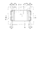
- FIG. 1A is a cross-sectional view of an electronic device according to a first embodiment of the present disclosure
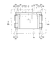
- 1B is a cross-sectional view taken along line IB-IB in FIG. 1A
- FIG. 2 is an enlarged cross-sectional view showing a heat conducting member and its vicinity of the electronic device according to the first embodiment of the present disclosure
- FIG. 3A is a cross-sectional view of an electronic device according to a second embodiment of the present disclosure
- 3B is a cross-sectional view taken along the line IIIB-IIIB of FIG. 3A.
- FIG. 4A is a cross-sectional view of an electronic device according to a third embodiment of the present disclosure; 4B is a cross-sectional view taken along the line IVB-IVB in FIG. 4A.
- FIG. 5A is a cross-sectional view of an electronic device according to a fourth embodiment of the present disclosure; 5B is a cross-sectional view taken along line VB-VB of FIG. 5A.
- FIG. 6A is a cross-sectional view of an electronic device according to a fifth embodiment of the present disclosure; 6B is a cross-sectional view taken along the line VIB-VIB of FIG. 6A.
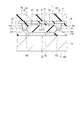
- FIGS. 1A and 1B An electronic device according to a first embodiment of the present disclosure is shown in FIGS. 1A and 1B.
- the electronic device 1 of the present embodiment is an inverter for driving, for example, a three-phase brushless motor.
- the electronic device 1 includes a heat sink 10 as a heat radiator, an electronic component 20, a heat conducting member 40, a joining member 50, and the like.
- the heat sink 10 is formed in a plate shape from a metal such as aluminum.
- the heat sink 10 has one surface 101 formed in a flat shape.
- the heat sink 10 has cooling fins 11 on the other surface 102 side.
- the electronic component 20 is provided on the one surface 101 side of the heat sink 10.
- the electronic component 20 includes an element 21, a sealing body 22, a terminal 23, and a heat sink 24.
- the element 21 is a switching element such as a MOS-FET. The element 21 generates heat during switching operation.
- the sealing body 22 is formed of an insulating material such as an epoxy resin.
- the sealing body 22 is formed in, for example, a rectangular plate shape.
- the sealing body 22 covers the entire element 21. Therefore, the element 21 is protected from external impacts and the like.
- the sealing body 22 includes an upper surface 31 that is one surface, a lower surface 32 that is the other surface, and side surfaces 33, 34, and 35 that are surfaces between the upper surface 31 and the lower surface 32. 36.
- the side surface 33 and the side surface 34 are side surfaces facing each other.
- the side surface 35 and the side surface 36 are side surfaces that face each other between the side surface 33 and the side surface 34.
- the side surfaces 33, 34, 35, and 36 of the sealing body 22 correspond to “the outer edge of the sealing body”.
- the side surface 33 includes an upper inclined surface 331 and a lower inclined surface 332.
- the upper inclined surface 331 is formed in a flat shape so as to be inclined with respect to the upper surface 31.
- the lower inclined surface 332 is formed in a flat shape so as to be inclined with respect to the lower surface 32.
- the side surface 34 includes an upper inclined surface 341 and a lower inclined surface 342.
- the upper inclined surface 341 is formed in a flat shape so as to be inclined with respect to the upper surface 31.
- the lower inclined surface 342 is formed in a flat shape so as to be inclined with respect to the lower surface 32.
- the electronic component 20 is provided such that the lower surface 32 of the sealing body 22 faces one surface 101 of the heat sink 10.
- the terminal 23 is formed in a plate shape by an electric conductor such as iron nickel alloy or copper. One end of the terminal 23 is embedded in the sealing body 22 such that one end protrudes outward from the side surfaces 33 and 34 of the sealing body 22, that is, the outer edge of the sealing body 22. In the present embodiment, a total of four terminals 23 are provided, two on each of the side surfaces 33 and 34 (see FIG. 1B).
- the terminal 23 has a protruding portion 231 and an inclined portion 232.
- the protruding portion 231 protrudes from the sealing body 22 so that one end thereof is substantially parallel to the upper surface 31 or the lower surface 32, and the other end is electrically connected to the element 21.
- the inclined portion 232 is formed integrally with the protruding portion 231 so as to extend toward the upper surface 31 while being inclined with respect to the protruding portion 231 (see FIG. 1A).
- the substrate 2 is provided on the opposite side of the electronic component 20 from the heat sink 10.
- the substrate 2 is, for example, a printed circuit board, and is provided so as to be substantially parallel to the heat sink 10 and the sealing body 22.
- the end of the inclined part 232 of the electronic component 20 opposite to the protruding part 231 is soldered to the printed wiring on the surface of the substrate 2.
- the heat radiating plate 24 is formed in a plate shape from a metal such as copper.
- the heat radiating plate 24 is provided on the sealing body 22 so as to be exposed from the lower surface 32 of the sealing body 22.
- the heat conducting member 40 is formed in a relatively flexible sheet shape and is provided between the heat sink 10 and the electronic component 20.
- the heat conducting member 40 includes a base material 41 and a filler 42.
- the base material 41 is, for example, a silicone resin.
- the filler 42 is, for example, granular aluminum oxide. That is, the heat conducting member 40 is a composite material of filler and resin.
- the base material 41 is set to a relatively small elastic modulus.
- the heat conducting member 40 is insulative.
- the heat conducting member 40 when the heat conducting member 40 is provided between the heat sink 10 and the electronic component 20, the heat conducting member 40 and the heat sink 10 or the heat radiating plate 24 are provided. Can be brought into close contact with each other.
- the thermal conductivity of the base material 41 is 0.2 W / mK.
- the thermal conductivity of the filler 42 is 20 to 36 W / mK.
- the heat conductive member 40 includes the filler 42 at a predetermined ratio with respect to the base material 41.
- the heat conducting member 40 is formed of a non-adhesive material.
- non-adhesive means a property that is always dry without stickiness and has an adhesive strength with other members of a predetermined value or less.
- Adhesiveness refers to the property of being sticky, constantly maintaining a wet state, and capable of adhering to other members. Therefore, if the heat conducting member 40 is simply provided between the heat sink 10 and the electronic component 20, the members can be easily separated from each other without adhering to each other. it can.
- the tensile shear bond strength (JIS K6850) between the heat conducting member 40 and the heat sink 10 or the electronic component 20 is, for example, 0.2 MPa or less.
- the linear expansion coefficient of the base material 41 is, for example, about 200 to 400 ppm.
- the linear expansion coefficient of the filler 42 is, for example, about 10 ppm.
- the linear expansion coefficient of the heat conducting member 40 is, for example, about 100 to 200 ppm. That is, the heat conducting member 40 includes the filler 42 with respect to the base material 41 at a ratio such that the linear expansion coefficient is about 100 to 200 ppm.
- the joining member 50 is formed of a thermosetting resin such as an epoxy resin. As shown in FIGS. 1A and 1B, in this embodiment, the joining member 50 is provided so as to cover the electronic component 20 in a state where the heat conducting member 40 is sandwiched between the joining member 50 and the heat sink 10. That is, the joining member 50 covers the side opposite to the heat conducting member 40 of the electronic component 20. In the present embodiment, the bonding member 50 also covers the substrate 2.
- the joining member 50 joins all the portions in the circumferential direction of the outer edge of the sealing body 22 of the electronic component 20 to the heat sink 10. More specifically, the bonding member 50 is bonded to one surface 101 of the heat sink 10 and the electronic component 20.
- Part of the bonding member 50 is located on the side surface 33 side and the side surface 34 side, and the side surface 35 side and the side surface 36 side of the sealing body 22 (see FIG. 1B). That is, the joining member 50 is located on both sides of the sealing body 22 of the electronic component 20 so that at least a part thereof sandwiches the sealing body 22 of the electronic component 20 therebetween. Further, a part of the joining member 50 is located on the side opposite to the heat sink 10 with respect to the terminal 23 (see FIGS. 1A and 1B).
- the linear expansion coefficient of the joining member 50 is about 50 to 90 ppm. That is, the joining member 50 has a linear expansion coefficient smaller than that of the heat conducting member 40. Further, the elastic modulus of the joining member 50 is larger than the elastic modulus of the heat conducting member 40. That is, the joining member 50 is less likely to be deformed than the heat conducting member 40.
- the manufacturing method of the electronic device 1 includes the following steps.
- (Soldering process) The terminal 23 of the electronic component 20 is soldered to the substrate 2.
- the heat conducting member 40 is provided at a predetermined position on one surface 101 of the heat sink 10.
- the electronic component 20 soldered to the substrate 2 is provided so that the heat radiating plate 24 is in contact with the heat conducting member 40.
- (Joining process) The liquid bonding member 50 is poured into the one surface 101 side of the heat sink 10 so as to cover the electronic component 20 and the substrate 2. Then, it heats. Thereby, the bonding member 50 is cured and bonded to the heat sink 10, the electronic component 20, and the substrate 2. As a result, the joining member 50 is in a state where the electronic component 20 and the heat sink 10 are joined.
- the heat conducting member 40 is joined to the joining member 50 due to the difference in linear expansion coefficient. Swells compared to As a result, the heat conducting member 40 expands between the heat sink 10 and the electronic component 20 and is in close contact with the heat sink 10 and the electronic component 20.
- the electronic device 1 includes the heat sink 10, the electronic component 20, the heat conducting member 40, and the joining member 50.
- the electronic component 20 is provided on the one surface 101 side of the heat sink 10 and generates heat during operation.
- the heat conducting member 40 is provided between the heat sink 10 and the electronic component 20 and can conduct heat from the electronic component 20 to the heat sink 10. Thereby, the heat at the time of the operation
- movement of the electronic component 20 can be thermally radiated from the heat sink 10 via the heat conductive member 40 effectively.
- the joining member 50 is provided so as to join at least a part in the circumferential direction of the outer edge of the electronic component 20 and the heat sink 10. Further, the joining member 50 has a linear expansion coefficient smaller than that of the heat conducting member 40. Therefore, when the temperature of the joining member 50 and the heat conducting member 40 rises to the same extent, the heat conducting member 40 expands compared to the joining member 50 due to the difference in coefficient of linear expansion. As a result, the heat conducting member 40 expands between the heat sink 10 and the electronic component 20 and is in close contact with the heat sink 10 and the electronic component 20.
- the electronic component 20 and the heat sink 10 are joined by the joining member 50, it is not necessary to use a curable adhesive as the heat conducting member 40. Therefore, at the time of manufacturing, after the heat conductive member 40 is provided between the electronic component 20 and the heat sink 10, a process such as a heat treatment for curing the heat conductive member 40, or the passage of a predetermined time is unnecessary. . Therefore, the manufacturing efficiency of the electronic device can be improved.
- the joining member 50 is positioned on both sides of the electronic component 20 so that at least a part of the joining member 50 sandwiches the electronic component 20 therebetween. Therefore, it is possible to effectively suppress the electronic component 20 from peeling off from the heat sink 10.
- the joining member 50 joins all the portions in the circumferential direction of the outer edge of the electronic component 20 to the heat sink 10. Therefore, it is possible to more effectively suppress the electronic component 20 from being peeled off from the heat sink 10.
- the joining member 50 covers the opposite side of the electronic component 20 from the heat conducting member 40. Therefore, it is possible to effectively suppress the electronic component 20 from peeling off from the heat sink 10 and to protect the electronic component 20 from external impacts, adhesion of foreign matters such as dust, and moisture.
- the joining member 50 is set so that the elastic modulus is larger than the elastic modulus of the heat conducting member 40. That is, the joining member 50 is less likely to be deformed than the heat conducting member 40. Therefore, when the temperature of the joining member 50 and the heat conducting member 40 rises, the heat conducting member 40 expands between the heat sink 10 and the electronic component 20, and the electronic component 20 is restricted from moving away from the heat sink 10. be able to. Thereby, the heat conductive member 40, the electronic component 20 and the heat sink 10 are more closely attached, and the heat of the electronic component 20 can be effectively radiated from the heat sink 10 via the heat conductive member 40. Therefore, the heat dissipation effect of the electronic component 20 can be maintained for a long time.
- the heat conducting member 40 is formed of a non-adhesive material. Therefore, in the manufacturing process of the electronic device 1, the heat conducting member 40 does not unintentionally adhere to other members, the manufacturing apparatus, or the like. That is, the heat conductive member 40 can be easily handled in the manufacturing process. Thereby, manufacturing efficiency can be improved.
- the electronic component 20 has the sealing body 22 and the terminal 23 embedded in the sealing body 22 so that one end protrudes outside from the outer edge end of the sealing body 22.
- a part of the joining member 50 is located on the side opposite to the heat sink 10 with respect to the terminal 23. Therefore, the side opposite to the heat sink 10 of the terminal 23 is locked by a part of the joining member 50, and it is possible to effectively suppress the electronic component 20 from being peeled off from the heat sink 10.
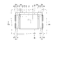
- FIGS. 3A and 3B An electronic device according to a second embodiment of the present disclosure is shown in FIGS. 3A and 3B.
- 2nd Embodiment differs in the structure of the joining member 50 from 1st Embodiment.
- the joining member 50 includes a virtual plane VP1 that includes the surface of the protruding portion 231 of the terminal 23 on the heat sink 10 side and is substantially parallel to one surface 101 of the heat sink 10. And a rectangular shape so as to be located within a predetermined range outside the sealing body 22.
- the joining member 50 includes a surface on the heat sink 10 side of the protruding portion 231 of the terminal 23, a lower inclined surface 332, a lower inclined surface 342, a part of the side surface 35, a part of the side surface 36, and a part of the side surface 36. It adheres to one surface 101 of the heat sink 10. That is, the joining member 50 joins all the portions in the circumferential direction of the outer edge of the sealing body 22 of the electronic component 20 to the heat sink 10.
- a part of the joining member 50 is located on the side surface 33 side and the side surface 34 side, and the side surface 35 side and the side surface 36 side of the sealing body 22 (see FIG. 3B). . That is, the joining member 50 is located on both sides of the sealing body 22 of the electronic component 20 so that at least a part thereof sandwiches the sealing body 22 of the electronic component 20 therebetween.
- the second embodiment is the same as the first embodiment except for the points described above.
- At least a part of the joining member 50 is located on both sides of the electronic component 20 with the electronic component 20 interposed therebetween. Therefore, it is possible to effectively suppress the electronic component 20 from peeling off from the heat sink 10.
- the joining member 50 joins all the portions in the circumferential direction of the outer edge of the electronic component 20 to the heat sink 10. Therefore, it is possible to more effectively suppress the electronic component 20 from being peeled off from the heat sink 10.
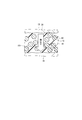
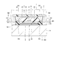
- FIGS. 4A and 4B An electronic device according to a third embodiment of the present disclosure is shown in FIGS. 4A and 4B.
- the third embodiment is different from the second embodiment in the configuration of the joining member 50.
- the joining member 50 is provided so as to be positioned on the side surface 33 side and the side surface 34 side of the sealing body 22 between the virtual plane VP1 and the one surface 101. It has been.
- the bonding member 50 is bonded to the surface of the protruding portion 231 of the terminal 23 on the heat sink 10 side, the lower inclined surface 332, the lower inclined surface 342, and one surface 101 of the heat sink 10. . That is, the joining member 50 joins a part of the outer edge of the sealing body 22 of the electronic component 20 in the circumferential direction to the heat sink 10.
- the bonding member 50 is located on the side surface 33 side and the side surface 34 side of the sealing body 22 (see FIG. 4B). That is, the joining member 50 is located on both sides of the sealing body 22 of the electronic component 20 so that at least a part thereof sandwiches the sealing body 22 of the electronic component 20 therebetween.
- the third embodiment is the same as the second embodiment except for the points described above.
- At least a part of the joining member 50 is located on both sides of the electronic component 20 with the electronic component 20 interposed therebetween. Therefore, it is possible to effectively suppress the electronic component 20 from peeling off from the heat sink 10.
- the joining member 50 joins a part of the outer edge of the sealing body 22 of the electronic component 20 in the circumferential direction to the heat sink 10. That is, in the third embodiment, the amount of the joining member 50 is small compared to the second embodiment. Therefore, compared with 2nd Embodiment, manufacturing cost can be reduced.
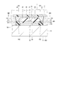
- FIGS. 5A and 5B An electronic device according to a fourth embodiment of the present disclosure is shown in FIGS. 5A and 5B. 4th Embodiment differs in the structure of the joining member 50 from 2nd Embodiment.
- the joining member 50 is located on the opposite side of the protruding portion 231 of the terminal 23 from the heat sink 10 and is substantially parallel to one surface 101 of the heat sink 10. Between VP ⁇ b> 2 and one surface 101, a rectangular shape is provided so as to be located within a predetermined range outside the sealing body 22.
- the joining member 50 includes a protruding portion 231 of the terminal 23, a part of the inclined portion 232, a lower inclined surface 332, a lower inclined surface 342, a part of the upper inclined surface 331, and an upper inclined surface 341. Part of the side surface 35, part of the side surface 36, and one surface 101 of the heat sink 10 are adhered. That is, the joining member 50 joins all the portions in the circumferential direction of the outer edge of the sealing body 22 of the electronic component 20 to the heat sink 10.
- a part of the joining member 50 is located on the side opposite to the heat sink 10 with respect to the protruding portion 231 of the terminal 23 (see FIGS. 5A and 5B). Further, a part of the joining member 50 is located on the opposite side to the heat sink 10 with respect to the upper inclined surface 331 and the upper inclined surface 341.
- the configuration of the fourth embodiment is the same as that of the second embodiment except for the points described above.
- a part of the joining member 50 is located on the side opposite to the heat sink 10 with respect to the terminal 23. Therefore, the side opposite to the heat sink 10 of the terminal 23 is locked by a part of the joining member 50, and it is possible to effectively suppress the electronic component 20 from being peeled off from the heat sink 10.
- a part of the joining member 50 is located on the opposite side to the heat sink 10 with respect to the upper inclined surface 331 and the upper inclined surface 341. Therefore, the upper inclined surface 331 and the upper inclined surface 341 are locked by a part of the joining member 50, and the electronic component 20 can be further effectively suppressed from being detached from the heat sink 10.
- FIGS. 6A and 6B An electronic device according to a fifth embodiment of the present disclosure is shown in FIGS. 6A and 6B.
- the fifth embodiment is different from the third embodiment in the configuration in the vicinity of the heat conducting member 40.
- the fifth embodiment further includes an adhesive material 3.
- the pressure-sensitive adhesive material 3 is, for example, a silicone-based grease that hardly changes in viscosity from room temperature to a predetermined high temperature. That is, the adhesive material 3 is an adhesive material.
- the adhesive material 3 includes a filler such as aluminum oxide.
- the adhesive material 3 is provided between the heat conducting member 40 and the heat sink 10 and between the heat conducting member 40 and the electronic component 20.
- the configuration of the fifth embodiment is the same as that of the third embodiment except for the points described above.
- the manufacturing method of the electronic device 1 includes the following steps.
- (Soldering process) The terminal 23 of the electronic component 20 is soldered to the substrate 2.
- (Adhesive material application process) The adhesive material 3 is applied to the surface on the heat sink 10 side of the heat conducting member 40 and the surface on the electronic component 20 side.
- (Thermal conduction member installation process) A heat conductive member 40 coated with the adhesive material 3 is provided at a predetermined position on one surface 101 of the heat sink 10. Since the adhesive material 3 is provided between the heat conductive member 40 and the heat sink 10, the position shift of the heat conductive member 40 with respect to the heat sink 10 can be suppressed after this step.
- the electronic component 20 soldered to the substrate 2 is provided so that the heat radiating plate 24 is in contact with the adhesive material 3. Since the adhesive material 3 is provided between the heat conducting member 40 and the electronic component 20, the positional displacement of the electronic component 20 with respect to the heat conducting member 40 can be suppressed after this step.
- the tensile shear adhesive strength (JISK6850) between the heat conducting member 40 and the heat sink 10 or the electronic component 20 through the adhesive material 3 is, for example, 0.2 MPa or less. Therefore, it is easy to correct the positions of the heat conducting member 40 and the electronic component 20 with respect to the heat sink 10.
- the liquid bonding member 50 is poured between the protruding portion 231 and the lower inclined surfaces 332 and 342 of the terminal 23 and the one surface 101 of the heat sink 10. Then, it heats. Thereby, the bonding member 50 is cured and bonded to the heat sink 10, the electronic component 20, and the substrate 2. As a result, the joining member 50 is in a state where the electronic component 20 and the heat sink 10 are joined.
- the present embodiment further includes the adhesive material 3 provided between the heat conducting member 40 and the heat sink 10 and between the heat conducting member 40 and the electronic component 20. Therefore, in the manufacturing process of the electronic device 1, it is possible to suppress the positional deviation between the heat conducting member 40, the heat sink 10, and the electronic component 20. Thereby, manufacturing efficiency can be improved.
- the heat conductive member 40 includes the filler 42 with respect to the base material 41 at such a ratio that the linear expansion coefficient is about 100 to 200 ppm is shown.
- the heat conductive member 40 includes the filler 42 in any ratio with respect to the base material 41 as long as the linear expansion coefficient is higher than the linear expansion coefficient of the bonding member 50. You may go out. Note that the higher the ratio of the filler 42 to the base material 41, the higher the thermal conductivity of the heat conducting member 40, but the smaller the linear expansion coefficient.
- the filler 42 is not limited to aluminum oxide, and may be a metal oxide such as zinc oxide or a nitride such as aluminum nitride or boron nitride. Further, if it is not necessary to ensure insulation between the electronic component 20 and the heat sink 10, the filler 42 may be an electric conductor such as metal or carbon.
- the bonding member 50 is not limited to an epoxy resin as long as the linear expansion coefficient is smaller than that of the heat conducting member 40, but is not limited to an epoxy resin, but is a thermosetting resin such as polyurethane or phenol resin, a thermoplastic resin, or photocuring. Resin etc. may be sufficient.
- the base material 41 of the heat conducting member 40 is formed of a non-adhesive silicone resin
- the base material 41 may be formed of, for example, silicone-based grease having adhesiveness as in the adhesive material 3 shown in the fifth embodiment.
- the base material 41 may be formed of, for example, a silicone material that is soft enough to maintain a sheet-like shape and has adhesiveness on the surface.
- the adhesive material 3 is provided on the heat sink 10 side and the electronic component 20 side of the heat conducting member 40 has been described.
- the adhesive material 3 may be provided on either the heat sink 10 side or the electronic component 20 side of the heat conducting member 40.
- the side surfaces 33 and 34 of the sealing body 22 of the electronic component 20 showed the example which consists of the upper inclined surface 331 and the lower inclined surface 332, the upper inclined surface 341, and the lower inclined surface 342, respectively.
- the side surfaces 33 and 34 may be formed in a planar shape that is substantially perpendicular to the upper surface 31 or the lower surface 32, as with the side surfaces 35 and 36.
- the shape is not limited to a rectangular plate shape, and may be any shape such as a polygon such as a triangle or a pentagon, or a circle.
- the example in which the terminal 23 of the electronic component 20 was formed in a plate shape was shown.
- the terminal 23 is not limited to a plate shape, and may be formed in a rod shape or the like, for example.
- the element 21 of the electronic component 20 is not limited to a switching element such as a MOS-FET, and may be another heating element. Moreover, the electronic component 20 may not have the heat sink 24. Further, the present disclosure is not limited to an inverter for driving a three-phase brushless motor, but can be used for various applications such as a driving device for other devices. Thus, the present disclosure is not limited to the above-described embodiment, and can be implemented in various forms without departing from the gist thereof.
Landscapes
- Engineering & Computer Science (AREA)
- Physics & Mathematics (AREA)
- Microelectronics & Electronic Packaging (AREA)
- Condensed Matter Physics & Semiconductors (AREA)
- General Physics & Mathematics (AREA)
- Computer Hardware Design (AREA)
- Power Engineering (AREA)
- Thermal Sciences (AREA)
- Chemical & Material Sciences (AREA)
- Materials Engineering (AREA)
- Cooling Or The Like Of Electrical Apparatus (AREA)
- Cooling Or The Like Of Semiconductors Or Solid State Devices (AREA)
Applications Claiming Priority (2)
| Application Number | Priority Date | Filing Date | Title |
|---|---|---|---|
| JP2016045439A JP6515841B2 (ja) | 2016-03-09 | 2016-03-09 | 電子装置 |
| JP2016-045439 | 2016-03-09 |
Publications (1)
| Publication Number | Publication Date |
|---|---|
| WO2017154923A1 true WO2017154923A1 (ja) | 2017-09-14 |
Family
ID=59790690
Family Applications (1)
| Application Number | Title | Priority Date | Filing Date |
|---|---|---|---|
| PCT/JP2017/009059 Ceased WO2017154923A1 (ja) | 2016-03-09 | 2017-03-07 | 電子装置 |
Country Status (2)
| Country | Link |
|---|---|
| JP (1) | JP6515841B2 (enExample) |
| WO (1) | WO2017154923A1 (enExample) |
Citations (5)
| Publication number | Priority date | Publication date | Assignee | Title |
|---|---|---|---|---|
| JP2004103641A (ja) * | 2002-09-05 | 2004-04-02 | Denso Corp | 半導体装置 |
| JP2005142328A (ja) * | 2003-11-06 | 2005-06-02 | Mitsubishi Electric Corp | 熱伝達装置 |
| JP2009170947A (ja) * | 2004-04-14 | 2009-07-30 | Denso Corp | 半導体装置 |
| JP2011239542A (ja) * | 2010-05-10 | 2011-11-24 | Mitsubishi Electric Corp | 車両用制御装置一体型回転電機 |
| JP2016143694A (ja) * | 2015-01-30 | 2016-08-08 | 三菱電機株式会社 | 半導体装置 |
Family Cites Families (2)
| Publication number | Priority date | Publication date | Assignee | Title |
|---|---|---|---|---|
| JP5898575B2 (ja) * | 2012-06-21 | 2016-04-06 | 日立オートモティブシステムズ株式会社 | 半導体装置 |
| JP6027945B2 (ja) * | 2013-06-05 | 2016-11-16 | 株式会社デンソー | 電子制御装置 |
-
2016
- 2016-03-09 JP JP2016045439A patent/JP6515841B2/ja active Active
-
2017
- 2017-03-07 WO PCT/JP2017/009059 patent/WO2017154923A1/ja not_active Ceased
Patent Citations (5)
| Publication number | Priority date | Publication date | Assignee | Title |
|---|---|---|---|---|
| JP2004103641A (ja) * | 2002-09-05 | 2004-04-02 | Denso Corp | 半導体装置 |
| JP2005142328A (ja) * | 2003-11-06 | 2005-06-02 | Mitsubishi Electric Corp | 熱伝達装置 |
| JP2009170947A (ja) * | 2004-04-14 | 2009-07-30 | Denso Corp | 半導体装置 |
| JP2011239542A (ja) * | 2010-05-10 | 2011-11-24 | Mitsubishi Electric Corp | 車両用制御装置一体型回転電機 |
| JP2016143694A (ja) * | 2015-01-30 | 2016-08-08 | 三菱電機株式会社 | 半導体装置 |
Also Published As
| Publication number | Publication date |
|---|---|
| JP6515841B2 (ja) | 2019-05-22 |
| JP2017162963A (ja) | 2017-09-14 |
Similar Documents
| Publication | Publication Date | Title |
|---|---|---|
| JP5813137B2 (ja) | 電力用半導体装置及びその製造方法 | |
| CN105073404B (zh) | 散热片以及使用了该散热片的散热结构体 | |
| JP2003168882A (ja) | 熱伝導性シート | |
| JP6127837B2 (ja) | 半導体装置 | |
| JP2003188323A (ja) | グラファイトシート及びその製造方法 | |
| JP6327140B2 (ja) | 電子装置 | |
| WO2016042739A1 (ja) | 放熱シートおよびこれを用いた放熱構造体 | |
| JP6337954B2 (ja) | 絶縁基板及び半導体装置 | |
| JP6164495B2 (ja) | 回路構成体及び回路構成体の製造方法 | |
| JP2003051573A (ja) | パワーモジュールとその製造方法 | |
| JP2016072354A (ja) | パワーモジュール | |
| JP2010192591A (ja) | 電力用半導体装置とその製造方法 | |
| JP2020061482A (ja) | 放熱構造 | |
| JP2013026296A (ja) | パワーモジュール | |
| JP6638567B2 (ja) | 半導体装置 | |
| WO2017154923A1 (ja) | 電子装置 | |
| JP5840102B2 (ja) | 電力用半導体装置 | |
| JP6168360B2 (ja) | 回路構成体及び回路構成体の製造方法 | |
| JP2008262948A (ja) | 電子部品ユニット | |
| JP2014135374A (ja) | 伝熱基板 | |
| JP2016111141A (ja) | 半導体装置 | |
| JP4807304B2 (ja) | 電子部品ユニット | |
| JP5987665B2 (ja) | 半導体装置 | |
| JPH0131700B2 (enExample) | ||
| JP2008066360A (ja) | 放熱性配線基板およびその製造方法 |
Legal Events
| Date | Code | Title | Description |
|---|---|---|---|
| NENP | Non-entry into the national phase |
Ref country code: DE |
|
| 121 | Ep: the epo has been informed by wipo that ep was designated in this application |
Ref document number: 17763263 Country of ref document: EP Kind code of ref document: A1 |
|
| 122 | Ep: pct application non-entry in european phase |
Ref document number: 17763263 Country of ref document: EP Kind code of ref document: A1 |