WO2017154530A1 - カードエッジコネクタ - Google Patents
カードエッジコネクタ Download PDFInfo
- Publication number
- WO2017154530A1 WO2017154530A1 PCT/JP2017/006050 JP2017006050W WO2017154530A1 WO 2017154530 A1 WO2017154530 A1 WO 2017154530A1 JP 2017006050 W JP2017006050 W JP 2017006050W WO 2017154530 A1 WO2017154530 A1 WO 2017154530A1
- Authority
- WO
- WIPO (PCT)
- Prior art keywords
- circuit board
- card edge
- fitting
- connector
- pressure receiving
- Prior art date
- Legal status (The legal status is an assumption and is not a legal conclusion. Google has not performed a legal analysis and makes no representation as to the accuracy of the status listed.)
- Ceased
Links
Images



Classifications
-
- H—ELECTRICITY
- H01—ELECTRIC ELEMENTS
- H01R—ELECTRICALLY-CONDUCTIVE CONNECTIONS; STRUCTURAL ASSOCIATIONS OF A PLURALITY OF MUTUALLY-INSULATED ELECTRICAL CONNECTING ELEMENTS; COUPLING DEVICES; CURRENT COLLECTORS
- H01R12/00—Structural associations of a plurality of mutually-insulated electrical connecting elements, specially adapted for printed circuits, e.g. printed circuit boards [PCB], flat or ribbon cables, or like generally planar structures, e.g. terminal strips, terminal blocks; Coupling devices specially adapted for printed circuits, flat or ribbon cables, or like generally planar structures; Terminals specially adapted for contact with, or insertion into, printed circuits, flat or ribbon cables, or like generally planar structures
- H01R12/70—Coupling devices
- H01R12/71—Coupling devices for rigid printing circuits or like structures
-
- H—ELECTRICITY
- H05—ELECTRIC TECHNIQUES NOT OTHERWISE PROVIDED FOR
- H05K—PRINTED CIRCUITS; CASINGS OR CONSTRUCTIONAL DETAILS OF ELECTRIC APPARATUS; MANUFACTURE OF ASSEMBLAGES OF ELECTRICAL COMPONENTS
- H05K1/00—Printed circuits
- H05K1/02—Details
Definitions
- the present invention relates to a card edge connector.
- Patent Document 1 discloses a card edge connector in which a circuit board is accommodated in a cover body having a flat cylindrical shape with a bottom, and a gap is filled between the cover body and the circuit board.
- the card edge portion on the circuit board where the terminals are arranged protrudes from the front surface of the cover body and is exposed.
- a mating connector is fitted to the front end portion of the cover body, and a contact provided on the mating connector comes into elastic contact with the terminal of the card edge portion.
- the circuit board is positioned by a guide formed on the cover body, and the movement of the circuit board is restricted by the solidified filler.
- the guide formed on the cover body is for sliding the circuit board when the circuit board is inserted into the cover body, there is a slight clearance between the guide and the circuit board. Therefore, the positioning accuracy of the circuit board with respect to the cover body is low, and there is a concern that the contact pressure with the contact of the counterpart connector may vary.
- the cover body and the filler are made of synthetic resin since insulation is required. Therefore, when the card edge connector is used in an environment where the temperature change is large, the circuit board moves with the thermal expansion and contraction of the cover body and the filler, and the contact between the card edge terminal and the counterpart connector And slide. When such sliding occurs, the contact resistance between the terminal of the card edge connector portion and the contact of the mating connector becomes unstable, and thus improvement is desired.
- the present invention has been completed based on the above-described circumstances, and an object thereof is to improve contact stability.
- the present invention A circuit board having a card edge portion in which a plurality of contacts are arranged in parallel; A substrate holder made of synthetic resin for accommodating the circuit board; A pressure receiving portion formed on the circuit board; It is characterized in that it comprises a pinching portion formed on the substrate holder so as to face each other at a narrower interval than the plate thickness of the pressure receiving portion, and holding the pressure receiving portion in a pressurized state by holding the pressure receiving portion in a pressurized state.
- the clamping part is formed so as to be opposed to each other at a distance narrower than the plate thickness of the pressure receiving part of the circuit board. Therefore, the circuit board is made into the board holder by the elastic deformation of the board holder and the plastic deformation of the clamping part. Therefore, the positioning can be performed reliably. Thereby, since the position of the contact with respect to the substrate holder is stabilized, the contact stability at the contact is improved.
- the front end portion of the board holder is formed with a fitting portion for fitting into a mating connector having a terminal fitting connectable to the contact, and the card edge portion is a front end edge of the circuit board.
- the pressure receiving part may be arranged at a position in front of the rear end part of the circuit board. When the pressure receiving part is arranged at the rear end of the circuit board, the card edge part moves back and forth as the board holder thermally expands and contracts. Then, sliding occurs and the contact resistance becomes unstable.
- the pressure receiving portion is sandwiched by the clamping portion at a position in front of the rear end portion of the circuit board, that is, at a position relatively close to the card edge portion, the amount of movement of the card edge portion in the front-rear direction can be suppressed small. . Thereby, since the sliding between a contact and a terminal metal fitting is also suppressed, contact stability is favorable.
- the present invention is a form in which the fitting portion protrudes forward in a cylindrical shape, the inside of the fitting portion is a connector housing space for housing the mating connector, You may distribute
- the front end of the pressure receiving portion is arranged at substantially the same position as the rear end of the connector housing space in the front-rear direction. It may be. According to this configuration, it is possible to visually confirm whether or not the circuit board is attached to a regular position with respect to the board holder.
- the fitting portion may be an insertion port for inserting the circuit board into the board holder.
- the board holder can be a single component with a bottomed cylindrical shape whose rear end is closed.
- the present invention may be configured such that the pressure receiving portion partially protrudes from a side edge portion in the width direction of the circuit board. According to this configuration, when the circuit board is attached to the substrate holder, the frictional resistance is generated between the pinching portion and the pressure receiving portion only in the final stage of the attachment process, so that workability is good.
- Example 1 A first embodiment embodying the present invention will be described below with reference to FIGS. In the following description, with respect to the front-rear direction, the left side in FIGS. Regarding the up and down directions, the directions appearing in FIGS.
- the connector of this embodiment includes a card edge connector A, a mating connector B, and a fitting spring 50.
- the card edge connector A includes a substrate holder 10 made of synthetic resin and a circuit board 30.
- the substrate holder 10 is a single part having a bottomed cylindrical shape with only the front end surface opened, and includes a substrate accommodating portion 11 and a fitting portion 23.
- substrate accommodating part 11 comprises the rear-end side part of the board
- the substrate housing portion 11 includes a pair of side wall portions 12 that are long and symmetrical in the front-rear direction, an upper wall portion 13 that connects upper end edges of both side wall portions 12, and both side wall portions 12.
- the lower wall part 14 which connects lower end edges of each other, and the rear wall part 15 connected to the rear end edges of the four wall parts 12, 13, and 14 are provided. That is, the board
- the internal space of the substrate housing portion 11 is a substrate housing space 16.
- a pair of symmetrical guide grooves 17 elongated in the front-rear direction are formed on the inner side surfaces of the left and right side wall portions 12.
- the guide groove 17 is formed continuously over a region from a position slightly behind the front end of the substrate housing portion 11 to the rearmost end of the substrate housing portion 11.
- the vertical spacing of the guide grooves 17 is set to be the same as or slightly larger than the plate thickness of the circuit board 30 described later.
- a pair of guide grooves 18 are formed at the foremost ends of the inner side surfaces of the left and right side wall portions 12 and are arranged outwardly in the left-right direction with respect to the guide grooves 17.
- the planar view shape of the pair of guide grooves 18 has a taper shape such that the distance between the left and right guide grooves 18 gradually narrows toward the rear.
- the front end of the guide groove 18 opens at the rear end of a connector housing space 26 described later.
- the rear end of the guide groove 18 is located slightly ahead of the front end of the guide groove 17.
- the left and right side wall portions 12 are formed with a pair of left and right symmetrical pinching portions 20 having concave inner surfaces.
- the pinching portion 20 is disposed so as to be sandwiched between the front end of the guide groove 17 and the rear end of the guide groove 18 in the front-rear direction.
- the pinching portion 20 is disposed at substantially the same height as the guide groove 17 and the guide groove 18 in the vertical direction.
- An internal space of the clamping unit 20 (a space between the pair of clamping surfaces 21) is open to the substrate housing space 16 on the inner surface of the side wall 12.
- the pinching portion 20 is arranged on the outer side of the guide groove 17 in the left-right direction (one farther from the inner surface of the side wall portion 12 than the guide groove 17). That is, the entire left pressing portion 20 is arranged to the left of the left edge of the left guide groove 17, and the entire right pressing portion 20 is the right edge of the right guide groove 17. It is arranged on the right side.
- the front end of the clamping unit 20 is continuous with the rear end of the guide groove 18.
- the internal space of the pinching portion 20 is opened to a space (a connector housing space 26 described later) ahead of the front end of the substrate housing portion 11 via the guide groove 18.
- the rear end surface of the pinching portion 20 serves as a stopper 22 that is perpendicular to the direction in which the circuit board 30 is inserted into the substrate housing portion 11.
- the stopper 22 restricts further insertion of the circuit board 30 when the circuit board 30 reaches the normal insertion position when the circuit board 30 is inserted into the board housing portion 11.
- Each pinching portion 20 has a pair of pinching surfaces 21 that face each other in the vertical direction.
- the pinching surface 21 is a flat surface parallel to the insertion direction of the circuit board 30 with respect to the substrate housing portion 11.
- the vertical dimension (interval) of the pair of clamping surfaces 21 is The dimension is set slightly smaller than the thickness of the pressure receiving portion 34 of the circuit board 30.
- the fitting part 23 includes a flange part 24 and a peripheral wall part 25.
- the flange portion 24 has a form that protrudes in the form of a rib from the outer peripheral edge of the front end portion of the substrate housing portion 11 to the outer surface side over the entire circumference.
- the front view shape of the flange portion 24 is a horizontally long substantially square shape.
- the peripheral wall portion 25 has a generally rectangular tube shape extending forward from the outer peripheral edge of the flange portion 24.
- the vertical dimension of the peripheral wall part 25 is larger than the vertical dimension of the substrate housing part 11, and the lateral dimension of the peripheral wall part 25 is larger than the lateral dimension of the substrate housing part 11.
- the internal space of the fitting portion 23 is a connector housing space 26 for housing the mating connector B.
- a front end of the connector housing space 26 is opened forward of the board holder 10, and a rear end of the connector housing space 26 communicates with the board housing space 16.
- a pair of left and right pressed surfaces 27 are formed on the left and right outer surfaces of the fitting portion 23.
- the pressed surface 27 is inclined with respect to the front-rear direction (a direction parallel to the fitting direction of both the connectors A and B).
- the front end surface of the fitting portion 23 becomes a fitting reference contact surface 28 that contacts the fitting reference receiving surface 45 of the counterpart connector B when the card edge connector A and the counterpart connector B are properly fitted.
- the front surface of the flange portion 24 faces the connector housing space 26.
- the front surface of the flange portion 24 (the back end surface of the connector housing space 26) serves as an insertion confirmation reference surface 29 for confirming the insertion depth of the circuit board 30 into the board housing space 16.
- the entire clamping portion 20 is disposed behind the insertion confirmation reference surface 29 (the rear end of the connector housing space 26).
- the circuit board 30 is formed of a flat plate whose shape in plan view is substantially square as a whole, and whose plate thickness dimension (vertical dimension) is substantially constant throughout.
- the circuit board 30 includes a board body 31 and a card edge 32.
- the entire substrate body 31 is accommodated in the substrate accommodating space 16.
- a printed circuit (not shown), a mounted electronic component such as a semiconductor, and the like are disposed on the board body 31.
- a plurality of contacts 33 arranged in the left-right direction are arranged on the card edge portion 32.
- a surface treatment by tin plating (not shown) is performed on the surface of the contact 33 (contact surface with a terminal fitting 48 described later).
- the card edge portion 32 is disposed in front of the substrate housing portion 11, that is, in the connector housing space 26.
- a pair of symmetrical pressure receiving portions 34 are formed at the front end portions of the left and right side edges of the substrate body portion 31.
- the pressure receiving portion 34 has a shape that protrudes from the side edge of the substrate body portion 31 outward in the left-right direction.
- the shape of the pressure receiving portion 34 in plan view is a square.
- the front end edge of the pressure receiving portion 34 is substantially perpendicular to the front-rear direction, and functions as an insertion confirmation edge portion 34F when the circuit board 30 is inserted into the board housing space 16.
- the rear end edge of the pressure receiving portion 34 is substantially perpendicular to the front-rear direction, and functions as the contact edge portion 34R when the circuit board 30 is inserted into the board housing space 16.
- a long region behind the pressure receiving portion 34 in both the left and right side edge portions of the substrate body portion 31 is a sliding contact edge portion that is in sliding contact with the guide groove 17 when the circuit board 30 is inserted into the substrate housing space 16. It functions as 35.
- the circuit board 30 When assembling the circuit board 30 to the board holder 10, the circuit board 30 is inserted from the front of the board holder 10. At this time, the connector housing space 26 of the fitting portion 23 functions as an insertion port 23 ⁇ / b> E for inserting the circuit board 30 into the board housing space 16.
- the circuit board 30 inserted into the fitting part 23 is accommodated in the board accommodating space 16 from the rear end side. At this time, both the left and right sliding contact edge portions 35 are fitted into the guide grooves 17 to be in sliding contact with each other, so that the circuit board 30 is positioned in the vertical and horizontal directions in the board housing space 16 and accommodates the board in a stable posture. It is inserted into the space 16. At this time, large friction does not occur between the sliding contact edge portion 35 and the guide groove 17.
- the pair of pressure receiving parts 34 are press-fitted into the pair of pressing parts 20.
- the front end portion of the pressure receiving portion 34 is positioned in front of the front end of the pressure sandwiching portion 20, only the rear end side region of the pressure receiving portion 34 is sandwiched by the pressure sandwiching portion 20.
- the substrate housing portion 11 is elastically deformed so as to widen the interval between the upper wall portion 13 and the lower wall portion 14 as a whole, and the pressure sandwiching surface 21 is rubbed against the pressure receiving portion 34 to be plastically deformed.
- a large frictional resistance is generated between the pinching part 20 and the pressure receiving part 34, but the large frictional resistance is generated only at the end of the insertion process of the circuit board 30.
- the contact edge portion 34R of the pressure receiving portion 34 comes into contact with the stopper 22 of the pinching portion 20 from the front, so that further insertion operation of the circuit board 30 is restricted.
- the insertion confirmation edge portion 34F of the pressure receiving portion 34 is aligned with the insertion confirmation reference surface 29 of the substrate holder 10 in a planar manner in a plan view. Therefore, it is possible to visually confirm whether or not the circuit board 30 has been inserted to the normal position based on the relative positional relationship in the front-rear direction of the insertion confirmation edge 34F with respect to the insertion confirmation reference plane 29.
- the pressure receiving portion 34 is sandwiched in the plate thickness direction in a pressurized state between the pair of upper and lower pressing surfaces 21 by the elastic deformation of the substrate housing portion 11 as described above. It becomes the press-fitted state.
- the circuit board 30 is moved in the front-rear direction and the left-right direction with respect to the board housing part 11 (board holder 10) by a large frictional force generated between the pressure-carrying surface 21 (clamping part 20) and the pressure-receiving part 34 by press-fitting (pressurization). Relative displacement is regulated.
- the clamping by the clamping surface 21 restricts the circuit board 30 from being displaced relative to the board housing part 11 (board holder 10) in the vertical direction.
- the mating connector B includes a synthetic resin housing 40 and a plurality of terminal fittings 48 accommodated in the housing 40 in parallel in the left-right direction.
- a surface treatment by tin plating (not shown) is performed on the surface of the terminal fitting 48 (the contact surface with the contact point 33 described above).
- the housing 40 includes a terminal accommodating portion 41 and a hood portion 42 that surrounds a front end side region of the terminal accommodating portion 41.
- a horizontally long slit-like substrate insertion groove 43 is formed that opens to the front surface (the surface facing the card edge connector A when fitted to the card edge connector A).
- An elastic contact portion (not shown) of the terminal fitting 48 faces the board insertion groove 43.
- the hood part 42 has a form protruding forward from the outer periphery of the terminal accommodating part 41.
- a space between the outer periphery of the terminal accommodating portion 41 and the inner periphery of the hood portion 42 is a fitting space 44 opened to the front of the housing 40.
- a spring receiving portion 46 is formed on the upper wall constituting the hood portion 42.
- a communication groove 47 that communicates from the outer peripheral surface of the hood portion 42 into the fitting space 44 is formed in the side wall that constitutes the hood portion 42. In a state where both connectors A and B are fitted, the communication groove 47 and the pressed surface 27 are positioned so as to correspond in the front-rear direction.
- the fitting spring 50 is made of a rod having a long and narrow spring property, and includes a pair of symmetrical long and narrow leg portions 51 and a connecting portion 52 that connects upper ends of both the leg portions 51.
- the connecting portion 52 of the fitting spring 50 is locked to the spring receiving portion 46 of the mating connector B, and both the leg portions 51 are accommodated in the communication groove 47 and pressed. It is elastically brought into contact with the surface 27. Thereby, both the connectors A and B are held in a state in which the fitting reference contact surface 28 and the fitting reference receiving surface 45 are in contact with each other.
- the card edge connector A includes the circuit board 30 having the card edge portion 32 in which a plurality of contacts 33 are arranged in parallel, the substrate holder 10 made of a synthetic resin that houses the circuit board 30, and the circuit.
- substrate holder 10 are provided.
- the pinching part 20 is formed so as to be opposed at an interval narrower than the plate thickness of the pressure receiving part 34, and is held in the movement restricted state by pinching the pressure receiving part 34 in a pressurized state.
- the clamping part 20 is formed so as to be opposed to each other at an interval narrower than the plate thickness of the pressure receiving part 34 of the circuit board 30, a circuit is formed by elastic deformation of the board holder 10 and plastic deformation of the clamping part 20.
- the substrate 30 can be reliably positioned with respect to the substrate holder 10. Thereby, since the position of the contact 33 with respect to the substrate holder 10 is stabilized, the contact stability at the contact 33 is improved.
- the front end portion of the board holder 10 is formed with a fitting portion 23 for fitting into a mating connector B having a terminal fitting 48 that can be connected to the contact 33, and the card edge portion 32 is formed at the front end of the circuit board 30. It is arranged at the edge. Therefore, when the pressure receiving portion 34 is disposed at the rear end portion of the circuit board 30, the card edge portion 32 moves back and forth as the substrate holder 10 is thermally expanded and contracted. There is a concern that sliding may occur between the terminal fitting 48 of B and the contact 33, resulting in unstable contact resistance.
- the pressure receiving portion 34 is located at a position in front of the rear end portion of the circuit board 30, that is, at a position relatively close to the card edge portion 32 (contact position between the contact 33 and the terminal fitting 48). Therefore, the amount of movement of the card edge portion 32 in the front-rear direction is kept small. Thereby, since the sliding between the contact 33 and the terminal metal fitting 48 is also suppressed, contact stability is good. Further, although the contact surface between the contact 33 and the terminal fitting 48 is tin-plated, the fine sliding wear between the contact 33 and the terminal fitting 48 is suppressed as described above. Even if the tin plating is relatively inexpensive, there is no risk of contact failure. As described above, the contact surface between the contact 33 and the terminal fitting 48 does not have to be subjected to expensive gold plating, so that cost reduction is realized.
- the fitting portion 23 has a form protruding in a cylindrical shape from the board housing portion 11, and the inside of the fitting portion 23 is a connector housing space 26 for housing the mating connector B.
- the pinching portion 20 is disposed behind the rear end (insertion confirmation reference surface 29) of the connector housing space 26. According to this configuration, since the space for arranging the pressing portion 20 inside the connector housing space 26 is not required, the size of the fitting portion 23 can be avoided.
- the insertion confirmation edge 34 ⁇ / b> F at the front end of the pressure receiving portion 34 is inserted into the insertion confirmation reference surface 29 at the rear end of the connector housing space 26 in the front-rear direction.
- the circuit board 30 is housed in a proper position with respect to the board holder 10
- the insertion confirmation edge 34 ⁇ / b> F at the front end of the pressure receiving portion 34 is inserted into the insertion confirmation reference surface 29 at the rear end of the connector housing space 26 in the front-rear direction.
- the fitting portion 23 serves as an insertion port 23E for inserting the circuit board 30 into the board holder 10. That is, the fitting part 23 has not only a function as a fitting means with the mating connector B but also a function as an insertion port 23 ⁇ / b> E of the circuit board 30. As a result, the substrate holder 10 is realized as a single component with a bottomed cylindrical shape whose rear end is closed.
- the pressure receiving portion 34 has a form partially protruding from the side edge portion in the width direction of the circuit board 30. According to this configuration, when the circuit board 30 is attached to the board holder 10, the frictional resistance is generated between the pinching part 20 and the pressure receiving part 34 only in the final stage of the attachment process. It is good.
- the present invention is not limited to the embodiments described with reference to the above description and drawings.
- the pressure receiving portion is disposed at a position ahead of the rear end portion of the circuit board, but the pressure receiving portion may be disposed at the rear end portion of the circuit board.
- the pinching portion is disposed behind the rear end of the connector housing space. However, the pinching portion may be disposed at a position ahead of the rear end of the connector housing space.
- the front end of the pressure receiving portion is arranged at substantially the same position as the rear end of the connector housing space in the front-rear direction, but the front end of the pressure receiving portion is located behind the connector housing space in the front-rear direction. You may make it distribute
- the circuit board is inserted into the board holder from the front, but the circuit board may be inserted into the board holder from the rear.
- the fitting portion has a shape that protrudes forward in a cylindrical shape, but the fitting portion has a form in which the front surface of the substrate holder is recessed, or a flange shape from the outer periphery of the front end of the substrate holder. An overhanging form may be used.
Landscapes
- Engineering & Computer Science (AREA)
- Microelectronics & Electronic Packaging (AREA)
- Coupling Device And Connection With Printed Circuit (AREA)
- Structure Of Printed Boards (AREA)
Abstract
接触安定性を高める カードエッジコネクタ(A)は、複数の接点(33)が並列されたカードエッジ部(32)を有する回路基板(30)と、回路基板(30)を収容する合成樹脂製の基板ホルダ(10)と、回路基板(30)に形成された受圧部(34)と、受圧部(34)の板厚より狭い間隔で対向するように基板ホルダ(10)に形成され、受圧部(34)を加圧状態で挟むことで移動規制状態に保持する挟圧部(20)とを備えている。
Description
本発明は、カードエッジコネクタに関するものである。
特許文献1には、有底の扁平な筒状をなすカバー体の内部に、回路基板を収容し、カバー体と回路基板の隙間に充填剤を充填したカードエッジコネクタが開示されている。回路基板のうち端子が配されているカードエッジ部は、カバー体の正面から突出して露出状態となっている。カバー体の前端部には相手方コネクタが嵌合され、相手方コネクタに設けたコンタクトが、カードエッジ部の端子に対し弾性的に接触するようになっている。カバー体の内部では、カバー体に形成したガイドによって回路基板が位置決めされ、固化した充填剤によって回路基板が移動規制されている。
カバー体に形成したガイドは、回路基板をカバー体内に挿入する際に回路基板を摺接させるものであるから、ガイドと回路基板との間には僅かではあるがクリアランスが存在する。そのため、カバー体に対する回路基板の位置決め精度が低く、相手方コネクタのコンタクトとの間の接触圧にばらつきが生じることが懸念される。
また、カバー体と充填剤は、絶縁性が求められることから合成樹脂を材料とする。そのため、カードエッジコネクタが温度変化の大きい環境下で使用される場合には、カバー体と充填剤の熱膨張及び熱収縮に伴って回路基板が移動し、カードエッジ部の端子と相手方コネクタのコンタクトとが摺動する。このような摺動が生じると、カードエッジコネク部の端子と相手方コネクタのコンタクトとの間の接触抵抗が不安定になるため、改善が望まれる。
本発明は上記のような事情に基づいて完成されたものであって、接触安定性を高めることを目的とする。
本発明は、
複数の接点が並列されたカードエッジ部を有する回路基板と、
前記回路基板を収容する合成樹脂製の基板ホルダと、
前記回路基板に形成された受圧部と、
前記受圧部の板厚より狭い間隔で対向するように前記基板ホルダに形成され、前記受圧部を加圧状態で挟むことで移動規制状態に保持する挟圧部とを備えているところに特徴を有する。
複数の接点が並列されたカードエッジ部を有する回路基板と、
前記回路基板を収容する合成樹脂製の基板ホルダと、
前記回路基板に形成された受圧部と、
前記受圧部の板厚より狭い間隔で対向するように前記基板ホルダに形成され、前記受圧部を加圧状態で挟むことで移動規制状態に保持する挟圧部とを備えているところに特徴を有する。
挟圧部は、回路基板の受圧部の板厚より狭い間隔で対向するように形成されたものであるから、基板ホルダの弾性変形と挟圧部の塑性変形とによって、回路基板を基板ホルダに対して確実に位置決めすることができる。これにより、基板ホルダを基準とする接点の位置が安定するので、接点における接触安定性が向上する。
本発明は、前記基板ホルダの前端部には、前記接点と接続可能な端子金具を有する相手側コネクタに嵌合するための嵌合部が形成され、前記カードエッジ部が前記回路基板の前端縁部に配され、前記受圧部が前記回路基板の後端部より前方の位置に配されていてもよい。受圧部が回路基板の後端部に配されている場合、基板ホルダが熱膨張及び熱収縮するのに伴ってカードエッジ部が前後に移動するため、相手側コネクタの端子金具と接点との間では、摺動が生じて接触抵抗が不安定となる。しかし、受圧部は回路基板の後端部より前方の位置、つまりカードエッジ部に比較的近い位置において挟圧部に挟み付けられているので、カードエッジ部の前後への移動量が小さく抑えられる。これにより、接点と端子金具との間の摺動も抑えられるので、接触安定性が良好である。
本発明は、前記嵌合部が前方へ筒状に突出した形態であり、前記嵌合部の内部は前記相手側コネクタを収容するためのコネクタ収容空間となっており、前記挟圧部は、前記コネクタ収容空間の後端より後方に配されていてもよい。この構成によれば、コネクタ収容空間の内部に挟圧部を配するスペースが不要なので、嵌合部の大型化を回避できる。
本発明は、前記回路基板が前記基板ホルダに対し正規の位置に収容された状態では、前記受圧部の前端が、前後方向において前記コネクタ収容空間の後端と概ね同じ位置に配されるようになっていてもよい。この構成によれば、回路基板が基板ホルダに対し正規の位置に取り付けられているか否かを、目視によって確認することが可能である。
本発明は、前記嵌合部が、前記基板ホルダ内へ前記回路基板を挿入するための挿入口となっていてもよい。この構成によれば、嵌合部が回路基板の挿入口としても機能も兼ね備えているので、基板ホルダを後端部が閉塞された有底筒状の単一部品とすることができる。
本発明は、前記受圧部が、前記回路基板の幅方向における側縁部から部分的に突出した形態であってもよい。この構成によれば、回路基板を基板ホルダに取り付ける際に、挟圧部と受圧部との間に摩擦抵抗が生じるのは、取り付け過程の最終期だけであるから、作業性が良い。
<実施例1>
以下、本発明を具体化した実施例1を図1~図6を参照して説明する。尚、以下の説明において、前後の方向については、図1~3,5,6における左方を前方と定義する。上下の方向については、図1,4,6にあらわれる向きを、そのまま上方、下方と定義する。
以下、本発明を具体化した実施例1を図1~図6を参照して説明する。尚、以下の説明において、前後の方向については、図1~3,5,6における左方を前方と定義する。上下の方向については、図1,4,6にあらわれる向きを、そのまま上方、下方と定義する。
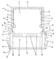
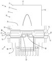
本実施例のコネクタは、カードエッジコネクタAと相手側コネクタBと嵌合バネ50とを備えている。カードエッジコネクタAは、合成樹脂製の基板ホルダ10と、回路基板30とを備えて構成されている。基板ホルダ10は、図3に示すように、前端面のみが開口した有底筒状をなす単一部品であり、基板収容部11と、嵌合部23とを備えている。基板収容部11は、基板ホルダ10の後端側部分を構成し、全体として幅寸法(左右寸法)に比べて上下寸法の小さい扁平な有底筒状をなしている。
図3,4に示すように、基板収容部11は、前後方向に細長く左右対称な一対の側壁部12と、両側壁部12の上端縁同士を連結する上壁部13と、両側壁部12の下端縁同士を連結する下壁部14と、上記4つの壁部12,13,14の後端縁に連なる後壁部15とを備えている。つまり、基板収容部11は、後端が閉塞された有底筒状をなしている。基板収容部11の内部空間は、基板収容空間16となっている。
左右両側壁部12の内側面には、前後方向に細長い左右対称な一対のガイド溝17が形成されている。ガイド溝17は、基板収容部11の前端より僅かに後方の位置から、基板収容部11の最後端に至る領域に亘って連続して形成されている。ガイド溝17の上下間隔は、後述する回路基板30の板厚寸法と同じか、それよりも僅かに大きい寸法に設定されている。
左右両側壁部12の内側面の最前端部には、ガイド溝17よりも左右方向において外方に配された一対の誘導溝18が形成されている。一対の誘導溝18の平面視形状は、両誘導溝18の左右間隔が後方に向かって次第に狭まるようなテーパ状をなしている。誘導溝18の前端は、後述するコネクタ収容空間26の後端部に開口している。誘導溝18の後端は、ガイド溝17の前端よりも少し前方に位置している。
左右両側壁部12には、その内側面を凹ませた形態の左右対称な一対の挟圧部20が形成されている。挟圧部20は、前後方向においてガイド溝17の前端と誘導溝18の後端との間に挟まれるように配されている。挟圧部20は、上下方向においてガイド溝17及び誘導溝18とほぼ同じ高さに配されている。挟圧部20の内部空間(一対の挟圧面21の間の空間)は、側壁部12の内側面において基板収容空間16に開放されている。挟圧部20は、左右方向において、ガイド溝17よりも外方(ガイド溝17に比べて側壁部12の内側面から遠い方)に配されている。つまり、左側の挟圧部20は、その全体が、左側のガイド溝17の左側縁よりも左方に配され、右側の挟圧部20は、その全体が、右側のガイド溝17の右側縁よりも右方に配されている。
挟圧部20の前端は誘導溝18の後端に連なっている。挟圧部20の内部空間は、誘導溝18を介して基板収容部11の前端よりも前方の空間(後述するコネクタ収容空間26)へ開放されている。挟圧部20の後端面は、基板収容部11に対する回路基板30の挿入方向と直角をなすストッパ22となっている。ストッパ22は、基板収容部11に回路基板30を挿入する際に、回路基板30が正規の挿入位置に到達すると、回路基板30のそれ以上の挿入を規制する。
各挟圧部20は、夫々、上下方向に対向する一対の挟圧面21を有している。挟圧面21は、基板収容部11に対する回路基板30の挿入方向と平行な平坦面である。挟圧面21が他部材と一度も接触していない未接触の状態(回路基板30が基板収容部11内に一度も挿入されていない状態)では、一対の挟圧面21の上下寸法(間隔)は、回路基板30の受圧部34の板厚寸法より僅かに小さい寸法に設定されている。
嵌合部23は、フランジ部24と周壁部25とを備えて構成されている。フランジ部24は、基板収容部11の前端部外周縁から全周に亘って外面側へリブ状に張り出した形態である。フランジ部24の正面視形状は、横長の略方形である。周壁部25は、フランジ部24の外周縁から前方へ延出した概ね角筒状をなしている。周壁部25の上下寸法は基板収容部11の上下寸法より大きく、周壁部25の左右寸法は基板収容部11の左右寸法より大きい。
嵌合部23の内部空間は、相手側コネクタBを収容するためのコネクタ収容空間26となっている。コネクタ収容空間26の前端は、基板ホルダ10の前方へ開放され、コネクタ収容空間26の後端は、基板収容空間16に連通している。嵌合部23の左右両外側面には、左右対称な一対の被押圧面27が形成されている。被押圧面27は、前後方向(両コネクタA,Bの嵌合方向と平行な方向)に対して傾斜している。
嵌合部23の前端面は、カードエッジコネクタAと相手側コネクタBが正規嵌合したときに、相手側コネクタBの嵌合基準受け面45に当接する嵌合基準当接面28となっている。コネクタ収容空間26の上下寸法は基板収容空間16の上下寸法より大きく、コネクタ収容空間26の左右寸法は基板収容空間16の左右寸法より大きいので、フランジ部24の前面はコネクタ収容空間26に臨んでいる。このフランジ部24の前面(コネクタ収容空間26の奥端面)は、基板収容空間16への回路基板30の挿入深さを確認するための挿入確認基準面29となっている。上記の挟圧部20は、その全体が、挿入確認基準面29(コネクタ収容空間26の後端)よりも後方に配置されている。
回路基板30は、平面視形状が全体として概ね方形をなし、板厚寸法(上下寸法)が全体に亘ってほぼ一定の平板からなる。回路基板30は、基板本体部31とカードエッジ部32とから構成されている。基板本体部31は、その全体が基板収容空間16内に収容されている。基板本体部31には、プリント回路(図示省略)や半導体等の実装電子部品等が配されている。カードエッジ部32には、左右方向に並ぶ複数の接点33が配されている。接点33の表面(後述する端子金具48との接触面)には、錫メッキ(図示省略)による表面処理が施されている。カードエッジ部32は、基板収容部11よりも前方、即ちコネクタ収容空間26内に配されている。
基板本体部31の左右両側縁の前端部には、左右対称な一対の受圧部34が形成されている。受圧部34は、基板本体部31の側縁から左右方向外方へ面一状に突出した形態である。受圧部34の平面視形状は方形である。受圧部34の前端縁は、前後方向に対して略直角であり、回路基板30を基板収容空間16内に挿入する際に挿入確認縁部34Fとして機能する。受圧部34の後端縁は、前後方向に対して略直角であり、回路基板30を基板収容空間16内に挿入する際に当接縁部34Rとして機能する。また、基板本体部31の左右両側縁部のうち受圧部34よりも後方の長尺の領域は、回路基板30を基板収容空間16内に挿入する際にガイド溝17に摺接する摺接縁部35として機能する。
回路基板30を基板ホルダ10に組み付ける際には、基板ホルダ10の前方から回路基板30を挿入する。このとき、嵌合部23のコネクタ収容空間26は、回路基板30を基板収容空間16内に挿入するための挿入口23Eとして機能する。嵌合部23内に挿入した回路基板30は、その後端部側から基板収容空間16内に収容されていく。このとき、左右両摺接縁部35をガイド溝17に嵌入して摺接されるので、回路基板30は、基板収容空間16内において上下方向及び左右方向において位置決めされ、安定した姿勢で基板収容空間16内に挿入される。このとき、摺接縁部35とガイド溝17との間で大きな摩擦が生じることはない。
基板収容空間16内への回路基板30の挿入過程の終盤に至ると、一対の受圧部34が一対の挟圧部20内に圧入される。このとき、受圧部34の前端部は、挟圧部20の前端よりも前方に位置するので、挟圧部20で挟み付けられるのは、受圧部34のうち後端側領域だけである。この圧入により、基板収容部11が、全体として上壁部13と下壁部14との間隔を広げるように弾性変形するとともに、挟圧面21が受圧部34に擦られて塑性変形する。これにより、挟圧部20と受圧部34との間で大きな摩擦抵抗が生じるのであるが、この大きな摩擦抵抗が生じるのは、回路基板30の挿入過程の終期のみである。
回路基板30が正規の位置まで挿入されると、受圧部34の当接縁部34Rが挟圧部20のストッパ22に対し前方から当接するので、回路基板30のそれ以上の挿入動作が規制される。また、受圧部34の挿入確認縁部34Fが、基板ホルダ10の挿入確認基準面29に対し平面視において面一状に並ぶ。したがって、挿入確認基準面29に対する挿入確認縁部34Fの前後方向の相対位置関係に基づいて、回路基板30が正規位置まで挿入されているか否かを目視で確認することができる。
回路基板30を正規挿入位置に挿入した状態では、上記のように基板収容部11の弾性変形により、受圧部34が、上下一対の挟圧面21の間で加圧状態で板厚方向に挟み付けられた圧入状態となる。圧入(加圧)によって挟圧面21(挟圧部20)と受圧部34との間に生じる大きな摩擦力により、回路基板30は、基板収容部11(基板ホルダ10)に対する前後方向及び左右方向への相対変位が規制される。また、挟圧面21による挟み付けにより、回路基板30は、基板収容部11(基板ホルダ10)に対する上下方向への相対変位が規制される。
相手側コネクタBは、合成樹脂製のハウジング40と、ハウジング40内に左右方向に並列して収容された複数の端子金具48とを備えている。端子金具48の表面(前述の接点33との接触面)には、錫メッキ(図示省略)による表面処理が施されている。ハウジング40は、端子収容部41と、端子収容部41の前端側領域を包囲するフード部42とを備えている。端子収容部41内には、その正面(カードエッジコネクタAとの嵌合時に、カードエッジコネクタAと対向する面)に開口する横長スリット状の基板挿入溝43が形成されている。端子金具48の弾性接触部(図示省略)は、基板挿入溝43内に臨んでいる。
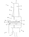
フード部42は、端子収容部41の外周から前方へ突出した形態である。端子収容部41の外周とフード部42の内周との間の空間は、ハウジング40の前方へ開放された嵌合空間44となっている。両コネクタA,Bが正規嵌合すると、端子収容部41がカードエッジコネクタAのコネクタ収容空間26内に収容され、嵌合空間44内には、カードエッジコネクタAの嵌合部23が嵌入される。両コネクタA,Bが正規嵌合すると、嵌合空間44の奥端面の嵌合基準受け面45に、カードエッジコネクタAの嵌合基準当接面28が当接する。これにより、両コネクタA,Bが前後方向において位置決めされる。また、両コネクタA,Bが嵌合した状態では、カードエッジ部32が基板挿入溝43に挿入され、端子金具48の弾性接触部が接点33に対上方又は下方から弾性的に当接する。
フード部42を構成する上面壁には、バネ受け部46が形成されている。フード部42を構成する側面壁には、フード部42の外周面から嵌合空間44内に連通する連通溝47が形成されている。両コネクタA,Bが嵌合した状態では、連通溝47と被押圧面27とが前後方向において対応するように位置する。嵌合バネ50は、細長いバネ性を有する棒材からなり、左右対称な一対の細長い脚部51と、両脚部51の上端部同士を連結する連結部52とを備えている。両コネクタA,Bを嵌合した後は、嵌合バネ50の連結部52を相手側コネクタBのバネ受け部46に係止するとともに、両脚部51を、連通溝47に収容して被押圧面27に対し弾性的に当接させる。これにより、両コネクタA,Bは、嵌合基準当接面28と嵌合基準受け面45とを当接させた状態に保持される。
上述のように、本実施例のカードエッジコネクタAは、複数の接点33が並列されたカードエッジ部32を有する回路基板30と、回路基板30を収容する合成樹脂製の基板ホルダ10と、回路基板30に形成された受圧部34と、基板ホルダ10に形成された挟圧部20とを備えている。挟圧部20は、受圧部34の板厚より狭い間隔で対向するように形成されており、受圧部34を加圧状態で挟むことで移動規制状態に保持する。挟圧部20は、回路基板30の受圧部34の板厚より狭い間隔で対向するように形成されたものであるから、基板ホルダ10の弾性変形と挟圧部20の塑性変形とによって、回路基板30を基板ホルダ10に対して確実に位置決めすることができる。これにより、基板ホルダ10を基準とする接点33の位置が安定するので、接点33における接触安定性が向上する。
また、基板ホルダ10の前端部には、接点33と接続可能な端子金具48を有する相手側コネクタBに嵌合するための嵌合部23が形成され、カードエッジ部32は回路基板30の前端縁部に配されている。そのため、受圧部34が回路基板30の後端部に配されていた場合には、基板ホルダ10が熱膨張及び熱収縮するのに伴ってカードエッジ部32が前後に移動するため、相手側コネクタBの端子金具48と接点33との間では、摺動が生じて接触抵抗が不安定となることが懸念される。
しかし、本実施例では、受圧部34が回路基板30の後端部より前方の位置、つまりカードエッジ部32(接点33と端子金具48との接触位置)に比較的近い位置において挟圧部20に挟み付けられているので、カードエッジ部32の前後への移動量が小さく抑えられている。これにより、接点33と端子金具48との間の摺動も抑えられるので、接触安定性が良好となっている。また、接点33と端子金具48との接触面には錫メッキが施されているのであるが、上記のように接点33と端子金具48との間での微摺動摩耗が抑えられているので、比較的安価な錫メッキであっても接触不良を生じる虞はない。このように、接点33と端子金具48との接触面には高価な金メッキを施さずに済んでいるので、コスト低減が実現されている。
また、嵌合部23は基板収容部11から前方へ筒状に突出した形態であり、嵌合部23の内部は相手側コネクタBを収容するためのコネクタ収容空間26となっている。そして、挟圧部20は、コネクタ収容空間26の後端(挿入確認基準面29)より後方に配されている。この構成によれば、コネクタ収容空間26の内部に挟圧部20を配するスペースが不要なので、嵌合部23の大型化を回避できる。
また、回路基板30は基板ホルダ10に対し正規の位置に収容された状態では、受圧部34の前端の挿入確認縁部34Fが、前後方向においてコネクタ収容空間26の後端の挿入確認基準面29と概ね同じ位置に配されるようになっている。この構成によれば、回路基板30が基板ホルダ10に対し正規の位置に取り付けられているか否かを、基板ホルダ10の前方から目視によって確認することが可能である。
また、嵌合部23は、基板ホルダ10内へ回路基板30を挿入するための挿入口23Eとなっている。つまり、嵌合部23が、相手側コネクタBとの嵌合手段としての機能だけでなく、回路基板30の挿入口23Eとしても機能も兼ね備えている。これにより、基板ホルダ10を後端部が閉塞された有底筒状の単一部品とすることが実現されている。
また、受圧部34は、回路基板30の幅方向における側縁部から部分的に突出した形態である。この構成によれば、回路基板30を基板ホルダ10に取り付ける際に、挟圧部20と受圧部34との間に摩擦抵抗が生じるのは、取り付け過程の最終期だけであるから、作業性が良好である。
<他の実施例>
本発明は上記記述及び図面によって説明した実施例に限定されるものではなく、例えば次のような実施例も本発明の技術的範囲に含まれる。
(1)上記実施例では、受圧部が回路基板の後端部よりも前方の位置に配されているが、受圧部は回路基板の後端部に配されていてもよい。
(2)上記実施例では、挟圧部をコネクタ収容空間の後端より後方に配したが、挟圧部はコネクタ収容空間の後端より前方の位置に配されていてもよい。
(3)上記実施例では、受圧部の前端が、前後方向においてコネクタ収容空間の後端と概ね同じ位置に配されるようにしたが、受圧部の前端は、前後方向においてコネクタ収容空間の後端より前方の位置、又はコネクタ収容空間の後端より後方の位置に配されるようにしてもよい。
(4)上記実施例では、回路基板を基板ホルダに対しその前方から挿入されるようにしたが、回路基板は、基板ホルダに対しその後方から挿入されるようにしてもよい。
(5)上記実施例では、嵌合部が前方へ筒状に突出した形状であるが、嵌合部は、基板ホルダの前面を凹ませた形態や、基板ホルダの前端部外周からフランジ状に張り出した形態であってもよい。
本発明は上記記述及び図面によって説明した実施例に限定されるものではなく、例えば次のような実施例も本発明の技術的範囲に含まれる。
(1)上記実施例では、受圧部が回路基板の後端部よりも前方の位置に配されているが、受圧部は回路基板の後端部に配されていてもよい。
(2)上記実施例では、挟圧部をコネクタ収容空間の後端より後方に配したが、挟圧部はコネクタ収容空間の後端より前方の位置に配されていてもよい。
(3)上記実施例では、受圧部の前端が、前後方向においてコネクタ収容空間の後端と概ね同じ位置に配されるようにしたが、受圧部の前端は、前後方向においてコネクタ収容空間の後端より前方の位置、又はコネクタ収容空間の後端より後方の位置に配されるようにしてもよい。
(4)上記実施例では、回路基板を基板ホルダに対しその前方から挿入されるようにしたが、回路基板は、基板ホルダに対しその後方から挿入されるようにしてもよい。
(5)上記実施例では、嵌合部が前方へ筒状に突出した形状であるが、嵌合部は、基板ホルダの前面を凹ませた形態や、基板ホルダの前端部外周からフランジ状に張り出した形態であってもよい。
A…カードエッジコネクタ
B…相手側コネクタ
10…基板ホルダ
20…挟圧部
23…嵌合部
23E…挿入口
26…コネクタ収容空間
30…回路基板
32…カードエッジ部
33…接点
34…受圧部
48…端子金具
B…相手側コネクタ
10…基板ホルダ
20…挟圧部
23…嵌合部
23E…挿入口
26…コネクタ収容空間
30…回路基板
32…カードエッジ部
33…接点
34…受圧部
48…端子金具
Claims (6)
- 複数の接点が並列されたカードエッジ部を有する回路基板と、
前記回路基板を収容する合成樹脂製の基板ホルダと、
前記回路基板に形成された受圧部と、
前記受圧部の板厚より狭い間隔で対向するように前記基板ホルダに形成され、前記受圧部を加圧状態で挟むことで移動規制状態に保持する挟圧部とを備えていることを特徴とするカードエッジコネクタ。 - 前記基板ホルダの前端部には、前記接点と接続可能な端子金具を有する相手側コネクタに嵌合するための嵌合部が形成され、
前記カードエッジ部が前記回路基板の前端縁部に配され、
前記受圧部が前記回路基板の後端部より前方の位置に配されていることを特徴とする請求項1記載のカードエッジコネクタ。 - 前記嵌合部が前方へ筒状に突出した形態であり、
前記嵌合部の内部は前記相手側コネクタを収容するためのコネクタ収容空間となっており、
前記挟圧部は、前記コネクタ収容空間の後端より後方に配されていることを特徴とする請求項2記載のカードエッジコネクタ。 - 前記回路基板が前記基板ホルダに対し正規の位置に収容された状態では、前記受圧部の前端が、前後方向において前記コネクタ収容空間の後端と概ね同じ位置に配されるようになっていることを特徴とする請求項3記載のカードエッジコネクタ。
- 前記嵌合部が、前記基板ホルダ内へ前記回路基板を挿入するための挿入口となっていることを特徴とする請求項2ないし請求項4のいずれか1項に記載のカードエッジコネクタ。
- 前記受圧部が、前記回路基板の幅方向における側縁部から部分的に突出した形態であることを特徴とする請求項1ないし請求項5のいずれか1項に記載のカードエッジコネクタ。
Priority Applications (1)
| Application Number | Priority Date | Filing Date | Title |
|---|---|---|---|
| CN201780015652.4A CN108780960A (zh) | 2016-03-11 | 2017-02-20 | 卡缘连接器 |
Applications Claiming Priority (2)
| Application Number | Priority Date | Filing Date | Title |
|---|---|---|---|
| JP2016-048204 | 2016-03-11 | ||
| JP2016048204A JP2017162762A (ja) | 2016-03-11 | 2016-03-11 | カードエッジコネクタ |
Publications (1)
| Publication Number | Publication Date |
|---|---|
| WO2017154530A1 true WO2017154530A1 (ja) | 2017-09-14 |
Family
ID=59789358
Family Applications (1)
| Application Number | Title | Priority Date | Filing Date |
|---|---|---|---|
| PCT/JP2017/006050 Ceased WO2017154530A1 (ja) | 2016-03-11 | 2017-02-20 | カードエッジコネクタ |
Country Status (3)
| Country | Link |
|---|---|
| JP (1) | JP2017162762A (ja) |
| CN (1) | CN108780960A (ja) |
| WO (1) | WO2017154530A1 (ja) |
Families Citing this family (3)
| Publication number | Priority date | Publication date | Assignee | Title |
|---|---|---|---|---|
| CN111541071B (zh) * | 2019-02-07 | 2024-03-15 | 泰科电子日本合同会社 | 连接器组件 |
| JP7287796B2 (ja) * | 2019-03-08 | 2023-06-06 | 株式会社ミクニ | 電子部品モジュール及びそのコネクタケース |
| CN112839455B (zh) * | 2019-11-22 | 2022-10-28 | 新电元工业株式会社 | 电子装置 |
Citations (4)
| Publication number | Priority date | Publication date | Assignee | Title |
|---|---|---|---|---|
| US20110097913A1 (en) * | 2009-10-22 | 2011-04-28 | Hon Hai Precision Industry Co., Ltd. | Card edge connector with an improved latch mechanism |
| JP2014130721A (ja) * | 2012-12-28 | 2014-07-10 | Auto Network Gijutsu Kenkyusho:Kk | カードエッジコネクタ |
| JP2015185210A (ja) * | 2014-03-20 | 2015-10-22 | 日本圧着端子製造株式会社 | カードエッジコネクタ |
| JP2016024942A (ja) * | 2014-07-18 | 2016-02-08 | 株式会社オートネットワーク技術研究所 | カードエッジコネクタ |
Family Cites Families (5)
| Publication number | Priority date | Publication date | Assignee | Title |
|---|---|---|---|---|
| DE102004005330A1 (de) * | 2004-02-04 | 2005-08-25 | Conti Temic Microelectronic Gmbh | Metallisches Gehäuse |
| CN201041841Y (zh) * | 2007-03-09 | 2008-03-26 | 富士康(昆山)电脑接插件有限公司 | 卡缘连接器 |
| JP5708424B2 (ja) * | 2011-10-05 | 2015-04-30 | 株式会社オートネットワーク技術研究所 | 外部接続が可能な電子回路ユニット |
| CN202872086U (zh) * | 2012-08-27 | 2013-04-10 | 立讯精密工业(昆山)有限公司 | 插头连接器及电连接器组合 |
| CN203423298U (zh) * | 2013-07-30 | 2014-02-05 | 东莞市奕联实业有限公司 | 迷你sas接口连接器 |
-
2016
- 2016-03-11 JP JP2016048204A patent/JP2017162762A/ja active Pending
-
2017
- 2017-02-20 WO PCT/JP2017/006050 patent/WO2017154530A1/ja not_active Ceased
- 2017-02-20 CN CN201780015652.4A patent/CN108780960A/zh active Pending
Patent Citations (4)
| Publication number | Priority date | Publication date | Assignee | Title |
|---|---|---|---|---|
| US20110097913A1 (en) * | 2009-10-22 | 2011-04-28 | Hon Hai Precision Industry Co., Ltd. | Card edge connector with an improved latch mechanism |
| JP2014130721A (ja) * | 2012-12-28 | 2014-07-10 | Auto Network Gijutsu Kenkyusho:Kk | カードエッジコネクタ |
| JP2015185210A (ja) * | 2014-03-20 | 2015-10-22 | 日本圧着端子製造株式会社 | カードエッジコネクタ |
| JP2016024942A (ja) * | 2014-07-18 | 2016-02-08 | 株式会社オートネットワーク技術研究所 | カードエッジコネクタ |
Also Published As
| Publication number | Publication date |
|---|---|
| CN108780960A (zh) | 2018-11-09 |
| JP2017162762A (ja) | 2017-09-14 |
Similar Documents
| Publication | Publication Date | Title |
|---|---|---|
| KR102167094B1 (ko) | 커넥터 | |
| JP5603790B2 (ja) | フローティング型コネクタ | |
| US8961215B2 (en) | Electrical connector assembled component, plug connector, and receptacle connector | |
| CN116169501B (zh) | 端子及链式端子 | |
| US20100159717A1 (en) | Board-To-Board Connector | |
| CN107134672B (zh) | 连接器 | |
| CN105428870B (zh) | 端子 | |
| CN113054450B (zh) | 端子模块、连接器以及嵌合结构 | |
| WO2014103404A1 (ja) | カードエッジコネクタ | |
| JP5880427B2 (ja) | カードエッジコネクタ | |
| CN106981754B (zh) | 连接器 | |
| CN107799948A (zh) | 用于电路基板用电连接器的限制件 | |
| JP6040964B2 (ja) | コネクタ | |
| US9853395B2 (en) | Connector and connector assembly | |
| CN102780111A (zh) | 压接型连接器 | |
| JP2022186850A (ja) | 可動コネクタ | |
| JP2017162762A (ja) | カードエッジコネクタ | |
| CN104412464A (zh) | 连接器 | |
| CN109004459B (zh) | 电连接器 | |
| JP6215119B2 (ja) | Usbレセプタクル | |
| KR20160058713A (ko) | 레버식 커넥터 | |
| JP2014241246A (ja) | コネクタ | |
| JP6118301B2 (ja) | 金型装置 | |
| JP2009508311A (ja) | プレロードをかけられたコンタクトプレートを備えた電気的な差し込みコネクタ | |
| WO2018131447A1 (ja) | コネクタ |
Legal Events
| Date | Code | Title | Description |
|---|---|---|---|
| NENP | Non-entry into the national phase |
Ref country code: DE |
|
| 121 | Ep: the epo has been informed by wipo that ep was designated in this application |
Ref document number: 17762873 Country of ref document: EP Kind code of ref document: A1 |
|
| 122 | Ep: pct application non-entry in european phase |
Ref document number: 17762873 Country of ref document: EP Kind code of ref document: A1 |