WO2017154171A1 - 画像取得装置および画像取得方法 - Google Patents
画像取得装置および画像取得方法 Download PDFInfo
- Publication number
- WO2017154171A1 WO2017154171A1 PCT/JP2016/057578 JP2016057578W WO2017154171A1 WO 2017154171 A1 WO2017154171 A1 WO 2017154171A1 JP 2016057578 W JP2016057578 W JP 2016057578W WO 2017154171 A1 WO2017154171 A1 WO 2017154171A1
- Authority
- WO
- WIPO (PCT)
- Prior art keywords
- signal
- control unit
- light
- image acquisition
- periodic signal
- Prior art date
- Legal status (The legal status is an assumption and is not a legal conclusion. Google has not performed a legal analysis and makes no representation as to the accuracy of the status listed.)
- Ceased
Links
Images



Classifications
-
- G—PHYSICS
- G01—MEASURING; TESTING
- G01N—INVESTIGATING OR ANALYSING MATERIALS BY DETERMINING THEIR CHEMICAL OR PHYSICAL PROPERTIES
- G01N21/00—Investigating or analysing materials by the use of optical means, i.e. using sub-millimetre waves, infrared, visible or ultraviolet light
- G01N21/62—Systems in which the material investigated is excited whereby it emits light or causes a change in wavelength of the incident light
- G01N21/63—Systems in which the material investigated is excited whereby it emits light or causes a change in wavelength of the incident light optically excited
- G01N21/64—Fluorescence; Phosphorescence
-
- G—PHYSICS
- G01—MEASURING; TESTING
- G01N—INVESTIGATING OR ANALYSING MATERIALS BY DETERMINING THEIR CHEMICAL OR PHYSICAL PROPERTIES
- G01N21/00—Investigating or analysing materials by the use of optical means, i.e. using sub-millimetre waves, infrared, visible or ultraviolet light
- G01N21/62—Systems in which the material investigated is excited whereby it emits light or causes a change in wavelength of the incident light
- G01N21/63—Systems in which the material investigated is excited whereby it emits light or causes a change in wavelength of the incident light optically excited
- G01N21/64—Fluorescence; Phosphorescence
- G01N21/645—Specially adapted constructive features of fluorimeters
- G01N21/6456—Spatial resolved fluorescence measurements; Imaging
- G01N21/6458—Fluorescence microscopy
-
- G—PHYSICS
- G02—OPTICS
- G02B—OPTICAL ELEMENTS, SYSTEMS OR APPARATUS
- G02B21/00—Microscopes
-
- G—PHYSICS
- G02—OPTICS
- G02B—OPTICAL ELEMENTS, SYSTEMS OR APPARATUS
- G02B21/00—Microscopes
- G02B21/0004—Microscopes specially adapted for specific applications
- G02B21/002—Scanning microscopes
- G02B21/0024—Confocal scanning microscopes (CSOMs) or confocal "macroscopes"; Accessories which are not restricted to use with CSOMs, e.g. sample holders
- G02B21/0052—Optical details of the image generation
- G02B21/0076—Optical details of the image generation arrangements using fluorescence or luminescence
-
- G—PHYSICS
- G02—OPTICS
- G02B—OPTICAL ELEMENTS, SYSTEMS OR APPARATUS
- G02B21/00—Microscopes
- G02B21/0004—Microscopes specially adapted for specific applications
- G02B21/002—Scanning microscopes
- G02B21/0024—Confocal scanning microscopes (CSOMs) or confocal "macroscopes"; Accessories which are not restricted to use with CSOMs, e.g. sample holders
- G02B21/008—Details of detection or image processing, including general computer control
-
- G—PHYSICS
- G01—MEASURING; TESTING
- G01N—INVESTIGATING OR ANALYSING MATERIALS BY DETERMINING THEIR CHEMICAL OR PHYSICAL PROPERTIES
- G01N21/00—Investigating or analysing materials by the use of optical means, i.e. using sub-millimetre waves, infrared, visible or ultraviolet light
- G01N21/62—Systems in which the material investigated is excited whereby it emits light or causes a change in wavelength of the incident light
- G01N21/63—Systems in which the material investigated is excited whereby it emits light or causes a change in wavelength of the incident light optically excited
- G01N21/64—Fluorescence; Phosphorescence
- G01N21/645—Specially adapted constructive features of fluorimeters
- G01N2021/6463—Optics
Definitions
- the present invention relates to an image acquisition device and an image acquisition method.
- the present invention has been made in view of the above-described circumstances, and an image acquisition apparatus and an image acquisition method capable of obtaining necessary sensitivity in a shorter exposure time compared to the case of using a lock-in amplifier. The purpose is to provide.
- a scanning unit that scans illumination light emitted from a light source, and the illumination light that is scanned by the scanning unit is collected on a sample, while signal light generated at each scanning position of the sample
- An optical system that collects the light, a detector that detects the signal light collected by the optical system and generates a detection signal, a signal control unit that generates a periodic signal repeated at a predetermined period, and the signal
- a light control unit that temporally controls the position or intensity of the illumination light according to the periodic signal generated by the control unit, and the detection signal generated by the detector according to the periodic signal generated by the signal control unit
- a calculation unit that processes the frequency of the detection signal by the period of the periodic signal generated by the signal control unit, and before the shift by the frequency shift unit.
- a detection signal which is an image acquisition device comprising an integrator for integrating an integer multiple of the integration time period of the periodic signal.
- each scanning position of the sample is irradiated via the optical system, and the signal light generated at each scanning position is collected by the optical system. Lighted. The collected signal light is detected by a detector to generate a detection signal, and the generated detection signal is processed in the arithmetic unit.
- the light control unit controls the irradiation position and intensity of the illumination light on the sample in accordance with the periodic signal generated by the signal control unit.
- the signal control unit generates the frequency of the detection signal generated by the detector. After being shifted by the frequency shift means by the period of the periodic signal, the integrator is integrated with an integration time that is an integral multiple of the period of the periodic signal in the integrator. Thereby, arbitrary signals can be separated and extracted from the detection signals detected in the mixed state.
- a lock-in amplifier is not used for signal separation and extraction, and an integrator that operates according to a periodic signal generated by the signal control unit is used.
- the required refresh rate is no longer necessary, and a signal with the required sensitivity is extracted with a shorter exposure time, and the extracted signal is applied to each scanning position, whereby an image of the sample can be acquired.
- the light control unit may alternately switch the position or intensity of the illumination light between two states according to the periodic signal.
- the signal control unit is configured to link the other two with reference to the periodic signal input to any one of the light control unit, the frequency shift unit, and the integrator. The phase of the periodic signal input to the other two may be adjusted.
- the said signal control part may be provided in either the said light control part, the said frequency shift means, and the said integrator.
- an A / D converter for digitizing the detection signal is provided, the frequency shift means assigns a digital code to the detection signal according to the periodic signal, and the integrator performs digital integration. May be.
- the A / D converter may have an offset adjustment function.
- the resolution of the detection signal can be improved by the A / D converter having the offset function.
- the illumination light is irradiated to the sample via a plurality of paths, and at least one of the light control unit, the signal control unit, and the calculation unit is configured so that each of the route passing through the path A plurality may be provided corresponding to the illumination light.
- a modulation step for temporally controlling the position or intensity of illumination light emitted from a light source according to a periodic signal repeated at a predetermined cycle, and the illumination light controlled in the modulation step A scanning step for scanning the sample, a detection step for detecting a signal light generated at each scanning position of the illumination light scanned in the scanning step to generate a detection signal, and the detection signal generated in the detection step A frequency shift step that shifts the frequency of the periodic signal by the period of the periodic signal, and an integration step that integrates the detection signal shifted by the frequency shift step with an integral time that is an integral multiple of the period of the periodic signal. It is an acquisition method.
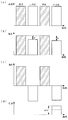
- FIG. 4 is a diagram illustrating detection signals after integration. It is a block diagram which shows the image acquisition method which concerns on one Embodiment of this invention. It is a block diagram which shows the 1st modification of the image acquisition apparatus of FIG. It is a block diagram which shows the 2nd modification of the image acquisition apparatus of FIG. It is a block diagram which shows the 3rd modification of the image acquisition apparatus of FIG. It is a block diagram which shows the 4th modification of the image acquisition apparatus of FIG. It is a block diagram which shows the 5th modification of the image acquisition apparatus of FIG.
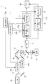
- the image acquisition apparatus 1 is a confocal microscope, and includes a light source 2 that emits laser light (illumination light), and a light control unit 3 that temporally modulates the position of the laser light from the light source 2. It has.
- the image acquisition apparatus 1 also collects a scanner (scanning unit) 4 that scans the laser beam temporally modulated by the light control unit 3 two-dimensionally and the laser beam scanned by the scanner 4 on the sample A.
- an objective lens (optical system) 5 that condenses the fluorescence generated at the irradiation position of the laser beam on the sample A is provided.
- the image acquisition device 1 also has a dichroic mirror 6 that separates the fluorescent light collected by the objective lens 5 and returned via the scanner 4 from the optical path of the laser light, and a position optically conjugate with the focal position of the objective lens 5.
- a pinhole 7 is provided, and a detector (PMT: photomultiplier tube) 8 that detects the fluorescence that has passed through the pinhole 7 and generates a detection signal.
- PMT photomultiplier tube
- the image acquisition apparatus 1 includes a calculation unit 9 that processes the detection signal generated by the detector 8 and an image processing unit (PC: personal computer) that generates an image based on the detection signal processed by the calculation unit 9. ) 10. Further, the light control unit 3 and the calculation unit 9 are connected to a signal control unit 11 that generates a predetermined periodic signal for synchronizing them.
- PC personal computer
- the light control unit 3 includes a first beam splitter 12 that branches the laser light from the light source 2 into two optical paths L1 and L2, and the optical paths L1 and L2 that are branched by the first beam splitter 12.
- a first beam splitter 12 that branches the laser light from the light source 2 into two optical paths L1 and L2, and the optical paths L1 and L2 that are branched by the first beam splitter 12.
- AOM acousto-optic modulators
- second beam splitter 14 for multiplexing the laser beams modulated by the acousto-optic modulators 13a and 13b.
- reference numeral 15 denotes a mirror for constituting an optical path.
- One optical path L1 is set so that the optical axis is shifted by the mirror 15 and the two laser beams combined by the second beam splitter 14 are incident on the scanner 4 at different angles.
- the laser beam that has passed through one optical path L1 is condensed at a position on the sample A that is optically non-conjugated with the pinhole 7.
- the laser beam that has passed through the other optical path L2 is condensed at a position on the sample A that is optically conjugate with the pinhole 7.
- the two acousto-optic modulators 13a and 13b operate exclusively according to the periodic signal output from the signal control unit 11.
- the laser light emitted from the light source 2 is a timing at which the intensity of the laser light passing through the two optical paths L1 and L2 is inverted by operating the two acousto-optic modulators 13a and 13b in synchronization with the periodic signal.
- FIG. 2 (a) the laser beam focused on the conjugate position and the laser beam focused on the non-conjugated position are alternately generated as shown in FIG.
- the two states with different laser light positions can be switched alternately in time.
- the calculation unit 9 includes an A / D converter (not shown), a frequency shift unit 16, and an integrator 17.
- the detection signal detected by the detector 8 is converted into a digital signal by an A / D converter and then input to the frequency shift means 16.
- the frequency shift means 16 shifts the frequency of the detection signal generated by the detector 8 by the period of the periodic signal generated by the signal control unit 11.
- the frequency shift means 16 is a digital frequency shift means that assigns a sign at a timing synchronized with a periodic signal, but may be a method of assigning positive or negative by a switch in an electric circuit, but is not limited thereto. Is not to be done.
- the integrator 17 integrates the output from the frequency shift means 16 with an integration time that is an integral multiple of the period of the periodic signal generated by the signal control unit 11. In the example shown in FIG. 2, integration is performed with an integration time twice as long as the period of the periodic signal.
- the output from the integrator 17 is shown in FIG. Thereby, only the fluorescence generated by subtracting the out-of-focus fluorescence from the fluorescence obtained by mixing the fluorescence generated at the focal position of the objective lens 5 and the out-of-focus fluorescence generated outside the focus, that is, the fluorescence generated at the focal position of the objective lens 5 only. Can be calculated.
- the image processing unit 10 generates a fluorescence image of the sample A by associating the fluorescence intensity output from the calculation unit 9 with the scanning position information by the scanner 4 when the fluorescence is detected. Yes. Since the fluorescence intensity output from the calculation unit 9 does not include the intensity of the out-of-focus fluorescence, a clear fluorescence image with little noise can be acquired.
- the image acquisition method according to the present embodiment is modulated by a modulation step S1 that temporally modulates the position of the laser light emitted from the light source 2 in accordance with a periodic signal generated at a predetermined period generated by the signal control unit 11.
- a scanning step S2 for scanning the sample A with the laser beam by the scanner 4 a detection step S3 for generating a detection signal by detecting fluorescence generated at each scanning position of the scanned laser beam, and a detection signal
- the frequency shift step S4 for shifting the frequency by the period of the periodic signal generated by the signal control unit 11, and the shifted detection signal are integrated with an integral time that is an integral multiple of the period of the periodic signal generated by the signal control unit 11. Integration step S5.
- the arithmetic unit 9 demodulates the fluorescence generated from the focal position of the objective lens 5 by the frequency shift means 16 and the integrator 17. Therefore, the refresh rate required when using the lock-in amplifier is unnecessary, and there is an advantage that a fluorescent image having a necessary sensitivity can be acquired with a short exposure time. On the contrary, there is an advantage that a sufficiently bright fluorescent image can be acquired by performing exposure with an exposure time for obtaining a fluorescent image having a necessary sensitivity by a lock-in amplifier.
- the present invention is not limited to this.
- the signal control unit 11 uses a periodic signal input to any one of the light control unit 3, the frequency shift unit 16, and the integrator 17 as a reference, and inputs the other two to interlock with the other two. You may have the phase adjustment function which adjusts the phase of a signal.
- the signal control unit 11 is described as a separate device from the light control unit 3, the frequency shift unit 16, and the integrator 17, but instead, the signal control unit 11 includes the light control unit 3, the frequency shift unit, and the frequency shift unit 16. Any one of the means 16 and the integrator 17 may be provided.
- the signal control unit 11 is provided in the light control unit 3, and the light control unit 3 is controlled by a periodic signal generated by itself, and the frequency shift means 16 and the integrator are controlled by the periodic signal generated by the light control unit 3. 17 may be controlled.
- a digital frequency shifter is adopted as the frequency shift means 16 of the arithmetic unit 9 and a digital integrator is adopted as the integrator 17. Since code assignment is performed by software after A / D conversion, there is an advantage that frequency shift can be performed without changing hardware even if the waveform of the signal changes.
- a multiplier made of an analog circuit may be adopted as the frequency shift means 16 and an integrator made of an analog circuit may be adopted as the integrator 17.
- an integrator made of an analog circuit may be adopted as the integrator 17.
- the frequency shift means 16 a multiplier made of an analog circuit may be adopted, an A / D converter for converting the output of the multiplier into a digital signal may be provided, and a digital integrator may be adopted.
- the A / D converter that converts the detection signal detected by the detector 8 into a digital signal is preferably provided with an offset adjustment function.
- the acoustooptic modulators 13a and 13b are used as the light control unit 3 has been exemplified.
- a combination with a plate or the like may be used.
- the laser light source itself may be directly controlled.
- a device that changes the direction of laser light such as an acousto-optic polarizer or an electro-optic polarizer, may be employed.
- the light source 18 is a laser light source that emits an ultrashort pulse laser beam
- the dichroic mirror 6 that branches fluorescence from the optical path of the ultrashort pulse laser beam is disposed between the objective lens 5 and the scanner 4.
- the pinhole 7 provided in FIG. 1 is excluded.
- two laser light sources (light sources) 19a and 19b that emit ultra-short pulse laser beams having different wavelengths, and ultra-short pulse laser beams from the laser light sources 19a and 19b, respectively, have different patterns.
- Two light control units 20a and 20b to modulate, two calculation units 21a and 21b that demodulate desired fluorescence from detected fluorescence, and two pairs of light control units 20a and 20b and calculation units 21a and 21b are different.
- Two signal controllers 22a and 22b for supplying periodic signals are provided. Thereby, two fluorescence signals can be acquired simultaneously.
- two pairs of signal control units 22a and 22b, light control units 20a and 20b, and arithmetic units 21a and 21b are provided, three or more pairs may be provided instead.
- only two calculation units 21 a and 21 b are provided, and the single light control unit 3 and the two pairs of calculation units 21 a and 21 b are synchronized by a periodic signal from the single signal control unit 11. May be activated.
- a multi-point scanner such as a Nipou disk is employed as the scanner 22, and a sensor array is employed as the detector 23.
- Two arithmetic units 21a and 21b are provided corresponding to the laser light passing through a plurality of optical paths branched by the Nipkow disk.
- the light modulation controls the light source intensity, switches the saturation / non-saturation of the focused fluorescence, and images the difference between the saturation / non-saturation, thereby improving resolution.
- two pairs of light sources 19a and 19b and light control units 20a and 20b are provided, and two light control units 20a and 20b and a single calculation unit 9 are connected to a single signal control unit 11.
- an SRS (Stimulated Raman Scattering) microscope that uses the vibration of the molecules of the sample A generated by the frequency difference when two types of laser beams having different frequencies are superimposed and irradiated onto the sample A is used. It can be applied to a nonlinear microscope.
- the two light sources 19a and 19b are laser light sources that emit ultrashort pulse laser beams having different wavelengths, respectively, and the periodic signal to the arithmetic unit 9 modulates one of the ultrashort pulse laser beams.
- the light control unit 20a Synchronized with the periodic signal to.
- a single laser light source 24 that emits an ultrashort pulse laser beam is adopted, and the two beams branched by the beam splitter 12 are used.
- the light control units 20a and 20b may be arranged on the two optical paths L1 and L2, respectively.
- two laser light sources 19a and 19b that emit an ultrashort pulse laser beam having the same wavelength may be employed.
Landscapes
- Physics & Mathematics (AREA)
- Chemical & Material Sciences (AREA)
- Analytical Chemistry (AREA)
- General Physics & Mathematics (AREA)
- Health & Medical Sciences (AREA)
- Optics & Photonics (AREA)
- Biochemistry (AREA)
- Life Sciences & Earth Sciences (AREA)
- Nuclear Medicine, Radiotherapy & Molecular Imaging (AREA)
- General Health & Medical Sciences (AREA)
- Immunology (AREA)
- Pathology (AREA)
- Engineering & Computer Science (AREA)
- Computer Vision & Pattern Recognition (AREA)
- General Engineering & Computer Science (AREA)
- Microscoopes, Condenser (AREA)
- Investigating, Analyzing Materials By Fluorescence Or Luminescence (AREA)
Abstract
ロックインアンプを使用する場合と比較して、より短い露光時間で、必要な感度を得ることを目的として、本発明に係る画像取得装置(1)は、光源(2)から射出された照明光を走査する走査部(4)と、走査される照明光を試料(A)に集光する一方、試料(A)の各走査位置において発生した信号光を集光する光学系(5)と、集光された信号光を検出して検出信号を生成する検出器(8)と、所定の周期で繰り返される周期信号を発生させる信号制御部(11)と、発生した周期信号に従い、照明光の位置または強度を時間的に制御する光制御部(3)と、発生した周期信号に従い、検出器(8)により生成された検出信号を処理する演算部(9)とを備え、演算部(9)が、周期信号の周期分だけ検出信号の周波数をシフトする周波数シフト手段(16)と、シフトされた検出信号を周期信号の周期の整数倍の積分時間で積分する積分器(17)とを備える。
Description
本発明は、画像取得装置および画像取得方法に関するものである。
強い信号に混じっている微小信号を検出して画像化するために、ロックインアンプを使用する画像取得方法が知られている(例えば、特許文献1から4参照。)。
特許文献1から4の技術のように微小信号の検出にロックインアンプを使用する場合、ロックインアンプのリフレッシュレート分だけ待たなければならず、必要な感度で微小信号を分離するために露光時間を増加させる必要がある。
本発明は、上述した事情に鑑みてなされたものであって、ロックインアンプを使用する場合と比較して、より短い露光時間で、必要な感度を得ることができる画像取得装置および画像取得方法を提供することを目的としている。
本発明は、上述した事情に鑑みてなされたものであって、ロックインアンプを使用する場合と比較して、より短い露光時間で、必要な感度を得ることができる画像取得装置および画像取得方法を提供することを目的としている。
本発明の一態様は、光源から射出された照明光を走査する走査部と、該走査部により走査される前記照明光を試料に集光する一方、該試料の各走査位置において発生した信号光を集光する光学系と、該光学系により集光された前記信号光を検出して検出信号を生成する検出器と、所定の周期で繰り返される周期信号を発生させる信号制御部と、該信号制御部が発生した前記周期信号に従い、前記照明光の位置または強度を時間的に制御する光制御部と、前記信号制御部が発生した前記周期信号に従い、前記検出器により生成された前記検出信号を処理する演算部とを備え、該演算部が、前記信号制御部が発生した前記周期信号の周期分だけ前記検出信号の周波数をシフトする周波数シフト手段と、該周波数シフト手段によりシフトされた前記検出信号を前記周期信号の周期の整数倍の積分時間で積分する積分器とを備える画像取得装置である。
本態様によれば、光源から射出された照明光が走査部によって走査されると、光学系を経由して試料の各走査位置に照射され、各走査位置において発生した信号光が光学系によって集光される。集光された信号光は検出器によって検出されることにより検出信号が生成され、生成された検出信号が演算部において処理される。
光制御部によって、試料における照明光の照射位置および強度が、信号制御部が発生した周期信号に従って制御され、演算部においては、検出器により生成された検出信号の周波数が、信号制御部が発生した周期信号の周期分だけ周波数シフト手段によってシフトされた後に、積分器において周期信号の周期の整数倍の積分時間で積分される。これにより、混合された状態で検出された検出信号の中から任意の信号を分離抽出することができる。
この場合において、本実施形態によれば、信号の分離抽出にロックインアンプを用いておらず、信号制御部が発生した周期信号に従って動作する積分器を用いているので、ロックインアンプにおいて必要であったリフレッシュレートが不要となり、より短い露光時間で必要な感度の信号を抽出し、抽出された信号を各走査位置に当てはめることで、試料の画像を取得することができる。
上記態様においては、前記光制御部が、前記周期信号に従い、前記照明光の位置または強度を2つの状態間で交互に切り替えてもよい。
また、上記態様においては、前記信号制御部が、前記光制御部、前記周波数シフト手段および前記積分器のいずれか1つに入力する前記周期信号を基準として、他の2つを連動させるように、他の2つに入力する前記周期信号の位相調整を行ってもよい。
また、上記態様においては、前記信号制御部が、前記光制御部、前記周波数シフト手段および前記積分器のいずれかに設けられていてもよい。
また、上記態様においては、前記信号制御部が、前記光制御部、前記周波数シフト手段および前記積分器のいずれか1つに入力する前記周期信号を基準として、他の2つを連動させるように、他の2つに入力する前記周期信号の位相調整を行ってもよい。
また、上記態様においては、前記信号制御部が、前記光制御部、前記周波数シフト手段および前記積分器のいずれかに設けられていてもよい。
また、上記態様においては、前記検出信号をデジタル化するA/D変換器を備え、前記周波数シフト手段が、前記周期信号に従って前記検出信号にデジタル符号割り当てを行い、前記積分器がデジタル積分を行ってもよい。
また、上記態様においては、前記A/D変換器が、オフセット調整機能を有していてもよい。
オフセット機能を有するA/D変換器により、検出信号の分解能を向上することができる。
オフセット機能を有するA/D変換器により、検出信号の分解能を向上することができる。
また、上記態様においては、前記照明光が複数の経路を経由して前記試料に照射され、前記光制御部、前記信号制御部および前記演算部の少なくとも1つが、各前記経路を経由する各前記照明光に対応して複数備えられていてもよい。
また、本発明の他の態様は、所定の周期で繰り返される周期信号に従って、光源から射出された照明光の位置または強度を時間的に制御する変調ステップと、該変調ステップにおいて制御された照明光を試料において走査する走査ステップと、該走査ステップにおいて走査された照明光の各走査位置において発生した信号光を検出して検出信号を生成する検出ステップと、該検出ステップにおいて生成された前記検出信号の周波数を、前記周期信号の周期分だけシフトする周波数シフトステップと、該周波数シフトステップによりシフトされた前記検出信号を前記周期信号の周期の整数倍の積分時間で積分する積分ステップとを含む画像取得方法である。
本発明によれば、ロックインアンプを使用する場合と比較して、より短い露光時間で、必要な感度を得ることができるという効果を奏する。
以下、本発明の一実施形態に係る画像取得装置1について、図面を参照して以下に説明する。
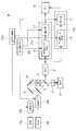
本実施形態に係る画像取得装置1は、共焦点顕微鏡であって、レーザ光(照明光)を射出する光源2と、光源2からのレーザ光の位置を時間的に変調する光制御部3とを備えている。また、画像取得装置1は、光制御部3により時間的に変調されたレーザ光を2次元的に走査するスキャナ(走査部)4と、該スキャナ4により走査されたレーザ光を試料Aに集光する一方、試料Aにおけるレーザ光の照射位置において発生した蛍光を集光する対物レンズ(光学系)5とを備えている。
本実施形態に係る画像取得装置1は、共焦点顕微鏡であって、レーザ光(照明光)を射出する光源2と、光源2からのレーザ光の位置を時間的に変調する光制御部3とを備えている。また、画像取得装置1は、光制御部3により時間的に変調されたレーザ光を2次元的に走査するスキャナ(走査部)4と、該スキャナ4により走査されたレーザ光を試料Aに集光する一方、試料Aにおけるレーザ光の照射位置において発生した蛍光を集光する対物レンズ(光学系)5とを備えている。
また、画像取得装置1は、対物レンズ5により集光されスキャナ4を経由して戻る蛍光をレーザ光の光路から分離するダイクロイックミラー6と、対物レンズ5の焦点位置と光学的に共役な位置に配置されるピンホール7と、該ピンホール7を通過した蛍光を検出し検出信号を生成する検出器(PMT:光電子増倍管)8とを備えている。
さらに、画像取得装置1は、検出器8において生成された検出信号を処理する演算部9と、該演算部9による処理後の検出信号に基づいて画像を生成する画像処理部(PC:パーソナルコンピュータ)10とを備えている。
また、光制御部3および演算部9にはこれらを同期させる所定の周期信号を発生する信号制御部11が接続されている。
また、光制御部3および演算部9にはこれらを同期させる所定の周期信号を発生する信号制御部11が接続されている。
本実施形態においては、光制御部3は、光源2からのレーザ光を2つの光路L1,L2に分岐する第1ビームスプリッタ12と、該第1ビームスプリッタ12により分岐された各光路L1,L2に設けられた音響光学変調器(AOM)13a,13bと、各音響光学変調器13a,13bにより変調されたレーザ光を合波する第2ビームスプリッタ14とを備えている。図中、符号15は、光路を構成するためのミラーである。
一方の光路L1は、ミラー15によって光軸をずらし、第2ビームスプリッタ14による合波後の2つのレーザ光がスキャナ4に異なる角度で入射するように設定されている。これにより、一方の光路L1を通過したレーザ光は、ピンホール7とは光学的に非共役な試料A上の位置に集光させられるようになっている。また、他方の光路L2を通過したレーザ光は、ピンホール7と光学的に共役な試料A上の位置に集光させられるようになっている。
2つの音響光学変調器13a,13bは、信号制御部11から出力される周期信号に従って、排他的に動作するようになっている。すなわち、光源2から発せられたレーザ光は、2つの音響光学変調器13a,13bを周期信号に同期して作動させることによって、2つの光路L1,L2を通過するレーザ光の強度を反転したタイミングで時間的に交互に増減させて、図2(a)に示されるように、共役な位置に集光されるレーザ光と、非共役な位置に集光されるレーザ光として交互に生成され、レーザ光の位置を異ならせた2つの状態が時間的に交互に切り替えられるようになっている。
演算部9は、図1に示されるように、図示しないA/D変換器と、周波数シフト手段16と積分器17とを備えている。
検出器8により検出された検出信号は、A/D変換器によってデジタル信号に変換された後に、周波数シフト手段16に入力されるようになっている。
検出器8により検出された検出信号は、A/D変換器によってデジタル信号に変換された後に、周波数シフト手段16に入力されるようになっている。
周波数シフト手段16は、検出器8により生成された検出信号の周波数を、信号制御部11が発生した周期信号の周期分だけシフトするようになっている。本実施形態においては、周波数シフト手段16は、周期信号に同期したタイミングで符号を割り当てるデジタル周波数シフト手段であるが、ほかに電気回路でスイッチにより正負を割り当てる方法であってもよく、これらに限定されるものではない。
例えば、図2(a)のレーザ光が試料Aに照射された結果、発生した蛍光が検出器8によって検出されることにより生成された検出信号が、図2(b)のようになった場合に周波数シフト手段16を通過させることにより、図2(c)に示されるように、非共役な位置において発生した蛍光の符号が反転させられる。
積分器17は、信号制御部11が発生した周期信号の周期の整数倍の積分時間で、周波数シフト手段16からの出力を積分するようになっている。図2に示す例では、周期信号の周期の2倍の積分時間で積分するようになっている。積分器17からの出力を図2(d)に示す。
これにより、対物レンズ5の焦点位置において発生した蛍光と焦点外において発生した焦点外蛍光とが混合された蛍光から焦点外蛍光を減算した蛍光、すなわち、対物レンズ5の焦点位置において発生した蛍光のみを算出することができるようになっている。
これにより、対物レンズ5の焦点位置において発生した蛍光と焦点外において発生した焦点外蛍光とが混合された蛍光から焦点外蛍光を減算した蛍光、すなわち、対物レンズ5の焦点位置において発生した蛍光のみを算出することができるようになっている。
画像処理部10は、演算部9から出力された蛍光強度を、該蛍光が検出された時点でのスキャナ4による走査位置情報と対応づけることにより、試料Aの蛍光画像を生成するようになっている。演算部9から出力された蛍光強度は、焦点外蛍光の強度を含まないので、ノイズの少ない鮮明な蛍光画像を取得することができる。
このように構成された本実施形態に係る画像取得装置1を用いた画像取得方法について、以下に説明する。
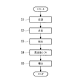
本実施形態に係る画像取得方法は、信号制御部11が発生した所定の周期で繰り返される周期信号に従って、光源2から射出されたレーザ光の位置を時間的に変調する変調ステップS1と、変調されたレーザ光をスキャナ4によって試料Aにおいて走査する走査ステップS2と、走査されたレーザ光の各走査位置において発生した蛍光を検出して検出信号を生成する検出ステップS3と、生成された検出信号の周波数を、信号制御部11が発生した周期信号の周期分だけシフトする周波数シフトステップS4と、シフトされた検出信号を信号制御部11が発生した周期信号の周期の整数倍の積分時間で積分する積分ステップS5とを含んでいる。
本実施形態に係る画像取得方法は、信号制御部11が発生した所定の周期で繰り返される周期信号に従って、光源2から射出されたレーザ光の位置を時間的に変調する変調ステップS1と、変調されたレーザ光をスキャナ4によって試料Aにおいて走査する走査ステップS2と、走査されたレーザ光の各走査位置において発生した蛍光を検出して検出信号を生成する検出ステップS3と、生成された検出信号の周波数を、信号制御部11が発生した周期信号の周期分だけシフトする周波数シフトステップS4と、シフトされた検出信号を信号制御部11が発生した周期信号の周期の整数倍の積分時間で積分する積分ステップS5とを含んでいる。
このように、本実施形態に係る画像取得装置1および画像取得方法によれば、演算部9が、周波数シフト手段16と積分器17によって対物レンズ5の焦点位置から発生した蛍光を復調しているので、ロックインアンプを用いる場合に必要であったリフレッシュレートが不要であり、短い露光時間で必要な感度の蛍光画像を取得することができるという利点がある。逆に、ロックインアンプにより必要な感度の蛍光画像を得るための露光時間で露光することにより、十分に明るい蛍光画像を取得することができるという利点がある。
なお、本実施形態においては、共焦点顕微鏡からなる画像取得装置1において、焦点外蛍光を除去した蛍光画像を取得する場合について説明したが、これに限定されるものではない。
信号制御部11は、光制御部3、周波数シフト手段16および積分器17のいずれか1つに入力する周期信号を基準として、他の2つを連動させるように他の2つに入力する周期信号の位相を調整する位相調整機能を有していてもよい。
信号制御部11は、光制御部3、周波数シフト手段16および積分器17のいずれか1つに入力する周期信号を基準として、他の2つを連動させるように他の2つに入力する周期信号の位相を調整する位相調整機能を有していてもよい。
また、信号制御部11を、光制御部3、周波数シフト手段16および積分器17とは別体の装置として記載したが、これに代えて、信号制御部11は、光制御部3、周波数シフト手段16および積分器17のいずれか1つに備えられていてもよい。
例えば、信号制御部11が光制御部3に備えられ、光制御部3がそれ自体で発生する周期信号によって制御されるとともに、光制御部3が発生する周期信号によって周波数シフト手段16および積分器17が制御されることにしてもよい。
例えば、信号制御部11が光制御部3に備えられ、光制御部3がそれ自体で発生する周期信号によって制御されるとともに、光制御部3が発生する周期信号によって周波数シフト手段16および積分器17が制御されることにしてもよい。
また、本実施形態においては、演算部9の周波数シフト手段16としてデジタル周波数シフタを採用し、積分器17としてデジタル積分器を採用した。A/D変換した後、符号割り当てをソフトウェアで行うので、信号の波形が変化してもハードウェアを変更せずに周波数シフトを行うことができるという利点がある。
これに代えて、周波数シフト手段16としてアナログ回路からなる乗算器を採用し、積分器17としてアナログ回路からなる積分器を採用してもよい。また、周波数シフト手段16として、アナログ回路からなる乗算器を採用し、乗算器の出力をデジタル信号に変換するA/D変換器を備えるとともに、デジタル積分器を採用してもよい。
周波数シフト手段16としてアナログ回路からなる乗算器を採用することにより、周波数シフトを正確に行うことができ、積分時に検出信号を取りこぼすことがないという利点がある。
また、積分器17としてデジタル積分器を採用することにより、コンデンサ開放の時間が不要となり高速処理を行うことができるという利点がある。
また、積分器17としてデジタル積分器を採用することにより、コンデンサ開放の時間が不要となり高速処理を行うことができるという利点がある。
また、検出器8により検出された検出信号をデジタル信号に変換するA/D変換器にオフセット調整機能が備えられていることが好ましい。
オフセット調整によってノイズを打ち消すことができるとともに、所望の信号に多くのメモリを割り当てることができダイナミックレンジを向上できるという利点がある。
オフセット調整によってノイズを打ち消すことができるとともに、所望の信号に多くのメモリを割り当てることができダイナミックレンジを向上できるという利点がある。
また、光制御部3として、音響光学変調器13a,13bを用いる場合を例示したが、これに代えて、レーザ光の強度を変調する音響光学素子、電気光学素子、NDフィルタ、波長板と偏光板との組み合わせ等を用いてもよい。また、レーザ光源そのものを直接制御してもよい。
また、光制御部3として、音響光学偏光器あるいは電気光学偏光器等のレーザ光の向きを変更するデバイスを採用してもよい。
また、光制御部3として、音響光学偏光器あるいは電気光学偏光器等のレーザ光の向きを変更するデバイスを採用してもよい。
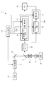
また、共焦点顕微鏡に代えて、図4から図6に示されるように、多光子励起顕微鏡を採用してもよいし、図7に示されるように、非線形顕微鏡を採用してもよい。
図4に示す例では、光源18は極短パルスレーザ光を射出するレーザ光源であり、蛍光を極短パルスレーザ光の光路から分岐するダイクロイックミラー6は、対物レンズ5とスキャナ4との間に配置されている。また、図1に備えられていたピンホール7が除外されている。
図4に示す例では、光源18は極短パルスレーザ光を射出するレーザ光源であり、蛍光を極短パルスレーザ光の光路から分岐するダイクロイックミラー6は、対物レンズ5とスキャナ4との間に配置されている。また、図1に備えられていたピンホール7が除外されている。
また、図5に示す例では、波長の異なる極短パルスレーザ光を射出する2つのレーザ光源(光源)19a,19bと、各レーザ光源19a,19bからの極短パルスレーザ光を異なるパターンでそれぞれ変調する2つの光制御部20a,20bと、検出された蛍光から所望の蛍光を復調する2つの演算部21a,21bと、2対の光制御部20a,20bおよび演算部21a,21bに対し異なる周期信号を供給する2つの信号制御部22a,22bとを備えている。これにより、2つの蛍光信号を同時に取得することができる。また、分光デバイスを備えていなくても分光することができるという利点がある。信号制御部22a,22b、光制御部20a,20bおよび演算部21a,21bを2対備えることとしたが、これに代えて、3対以上備えていてもよい。
また、図6に示すように、演算部21a,21bのみ2つ備え、単一の光制御部3および2対の演算部21a,21bを単一の信号制御部11からの周期信号によって同期して作動させることにしてもよい。この例では、スキャナ22としてニポウディスクのような多点スキャナを採用し、検出器23としてセンサアレイを採用している。ニポウディスクによって分岐された複数の光路を経由するレーザ光に対応して2つの演算部21a,21bが備えられている。光変調が光源強度を制御し、焦点蛍光の飽和/非飽和を切り替え、飽和/非飽和の差分を画像化することで解像度を向上させることができる。
また、図7に示すように、光源19a,19bおよび光制御部20a,20bを2対備え、2つの光制御部20a,20bおよび単一の演算部9を単一の信号制御部11からの周期信号によって同期して作動させることにしてもよい。このように構成することで、周波数の異なる2種類のレーザ光を重ねて試料Aに照射する際に周波数差によって発生する試料Aの分子の振動を利用するSRS(誘導ラマン散乱)顕微鏡のような非線形顕微鏡に適用することができる。2つの光源19a,19bは、それぞれ波長の異なる極短パルスレーザ光を射出するレーザ光源であり、演算部9への周期信号は一方の極短パルスレーザ光を変調する、例えば、光制御部20aへの周期信号と同期している。
また、図8に示されるように、図5の2つのレーザ光源19a,19bに代えて、極短パルスレーザ光を射出する単一のレーザ光源24を採用し、ビームスプリッタ12によって分岐された2つの光路L1,L2にそれぞれ光制御部20a,20bを配置してもよい。ビームスプリッタ12を用いることなく、同一の波長の極短パルスレーザ光を射出する2つのレーザ光源19a,19bを採用してもよい。異なる位置に集光する極短パルスレーザ光を異なる繰り返し周期で変調し、2つの演算部9によって復調することにより、2点の信号を同時に取得でき、画像取得速度の向上を図ることができる。
1 画像取得装置
2,24 光源
3,20a,20b 光制御部
4,22 スキャナ(走査部)
5 対物レンズ(光学系)
8,23 検出器
9,21a,21b 演算部
11,22a,22b 信号制御部
16 周波数シフト手段
17 積分器
19a,19b レーザ光源(光源)
A 試料
S1 変調ステップ
S2 走査ステップ
S3 検出ステップ
S4 周波数シフトステップ
S5 積分ステップ
2,24 光源
3,20a,20b 光制御部
4,22 スキャナ(走査部)
5 対物レンズ(光学系)
8,23 検出器
9,21a,21b 演算部
11,22a,22b 信号制御部
16 周波数シフト手段
17 積分器
19a,19b レーザ光源(光源)
A 試料
S1 変調ステップ
S2 走査ステップ
S3 検出ステップ
S4 周波数シフトステップ
S5 積分ステップ
Claims (8)
- 光源から射出された照明光を走査する走査部と、
該走査部により走査される前記照明光を試料に集光する一方、該試料の各走査位置において発生した信号光を集光する光学系と、
該光学系により集光された前記信号光を検出して検出信号を生成する検出器と、
所定の周期で繰り返される周期信号を発生させる信号制御部と、
該信号制御部が発生した前記周期信号に従い、前記照明光の位置または強度を時間的に制御する光制御部と、
前記信号制御部が発生した前記周期信号に従い、前記検出器により生成された前記検出信号を処理する演算部とを備え、
該演算部が、前記信号制御部が発生した前記周期信号の周期分だけ前記検出信号の周波数をシフトする周波数シフト手段と、該周波数シフト手段によりシフトされた前記検出信号を前記周期信号の周期の整数倍の積分時間で積分する積分器とを備える画像取得装置。 - 前記光制御部が、前記周期信号に従い、前記照明光の位置または強度を2つの状態間で交互に切り替える請求項1に記載の画像取得装置。
- 前記信号制御部が、前記光制御部、前記周波数シフト手段および前記積分器のいずれか1つに入力する前記周期信号を基準として、他の2つを連動させるように、他の2つに入力する前記周期信号の位相調整を行う請求項1または請求項2に記載の画像取得装置。
- 前記信号制御部が、前記光制御部、前記周波数シフト手段および前記積分器のいずれかに設けられている請求項3に記載の画像取得装置。
- 前記検出信号をデジタル化するA/D変換器を備え、
前記周波数シフト手段が、前記周期信号に従って前記検出信号にデジタル符号割り当てを行い、
前記積分器がデジタル積分を行う請求項1から請求項4のいずれかに記載の画像取得装置。 - 前記A/D変換器が、オフセット調整機能を有する請求項5に記載の画像取得装置。
- 前記照明光が複数の経路を経由して前記試料に照射され、
前記光制御部、前記信号制御部および前記演算部の少なくとも1つが、各前記経路を経由する各前記照明光に対応して複数備えられている請求項1から請求項6のいずれかに記載の画像取得装置。 - 所定の周期で繰り返される周期信号に従って、光源から射出された照明光の位置または強度を時間的に制御する変調ステップと、
該変調ステップにおいて制御された照明光を試料において走査する走査ステップと、
該走査ステップにおいて走査された照明光の各走査位置において発生した信号光を検出して検出信号を生成する検出ステップと、
該検出ステップにおいて生成された前記検出信号の周波数を、前記周期信号の周期分だけシフトする周波数シフトステップと、
該周波数シフトステップによりシフトされた前記検出信号を前記周期信号の周期の整数倍の積分時間で積分する積分ステップとを含む画像取得方法。
Priority Applications (3)
| Application Number | Priority Date | Filing Date | Title |
|---|---|---|---|
| JP2018503945A JP6599539B2 (ja) | 2016-03-10 | 2016-03-10 | 画像取得装置および画像取得方法 |
| PCT/JP2016/057578 WO2017154171A1 (ja) | 2016-03-10 | 2016-03-10 | 画像取得装置および画像取得方法 |
| US16/102,840 US10261299B2 (en) | 2016-03-10 | 2018-08-14 | Image-acquisition apparatus and image-acquisition method |
Applications Claiming Priority (1)
| Application Number | Priority Date | Filing Date | Title |
|---|---|---|---|
| PCT/JP2016/057578 WO2017154171A1 (ja) | 2016-03-10 | 2016-03-10 | 画像取得装置および画像取得方法 |
Related Child Applications (1)
| Application Number | Title | Priority Date | Filing Date |
|---|---|---|---|
| US16/102,840 Continuation US10261299B2 (en) | 2016-03-10 | 2018-08-14 | Image-acquisition apparatus and image-acquisition method |
Publications (1)
| Publication Number | Publication Date |
|---|---|
| WO2017154171A1 true WO2017154171A1 (ja) | 2017-09-14 |
Family
ID=59789280
Family Applications (1)
| Application Number | Title | Priority Date | Filing Date |
|---|---|---|---|
| PCT/JP2016/057578 Ceased WO2017154171A1 (ja) | 2016-03-10 | 2016-03-10 | 画像取得装置および画像取得方法 |
Country Status (3)
| Country | Link |
|---|---|
| US (1) | US10261299B2 (ja) |
| JP (1) | JP6599539B2 (ja) |
| WO (1) | WO2017154171A1 (ja) |
Cited By (1)
| Publication number | Priority date | Publication date | Assignee | Title |
|---|---|---|---|---|
| JP2024510596A (ja) * | 2021-03-11 | 2024-03-08 | ザ・トラスティーズ・オブ・コロンビア・ユニバーシティ・イン・ザ・シティ・オブ・ニューヨーク | 掃引共焦点配置平面励起(scape)顕微鏡法 |
Families Citing this family (1)
| Publication number | Priority date | Publication date | Assignee | Title |
|---|---|---|---|---|
| US12248133B2 (en) * | 2021-01-22 | 2025-03-11 | The Hong Kong University Of Science And Technology | Methods and apparatus for in vivo high resolution multiphoton microscopy |
Citations (3)
| Publication number | Priority date | Publication date | Assignee | Title |
|---|---|---|---|---|
| JP2011199939A (ja) * | 2010-03-17 | 2011-10-06 | Hitachi Ltd | 電力変換装置および電力変換装置の制御方法 |
| JP2014120862A (ja) * | 2012-12-14 | 2014-06-30 | Sony Corp | 通信装置 |
| WO2015163261A1 (ja) * | 2014-04-24 | 2015-10-29 | オリンパス株式会社 | 顕微鏡および顕微鏡観察方法 |
Family Cites Families (17)
| Publication number | Priority date | Publication date | Assignee | Title |
|---|---|---|---|---|
| GB0200819D0 (en) * | 2002-01-15 | 2002-03-06 | Cole Polytechnique Federale De | Microscopy imaging apparatus and method for generating an image |
| WO2006061947A1 (ja) | 2004-12-08 | 2006-06-15 | Osaka University | 蛍光顕微鏡及び観察方法 |
| JP5448353B2 (ja) * | 2007-05-02 | 2014-03-19 | キヤノン株式会社 | 光干渉断層計を用いた画像形成方法、及び光干渉断層装置 |
| US8111455B2 (en) | 2007-11-26 | 2012-02-07 | Olympus Corporation | Light source apparatus and laser scanning microscope |
| JP5231154B2 (ja) | 2007-11-26 | 2013-07-10 | オリンパス株式会社 | レーザ走査型顕微鏡 |
| DE102008059328A1 (de) * | 2008-11-27 | 2010-06-02 | Carl Zeiss Microimaging Gmbh | Auflösungsgesteigerte Mikroskopie |
| US8531677B2 (en) * | 2010-05-27 | 2013-09-10 | Corning Incorporated | Frequency-shifting interferometer with selective data processing |
| DE102010047237B4 (de) | 2010-08-13 | 2021-07-01 | Leica Microsystems Cms Gmbh | Verfahren zum Trennen von Detektionssignalen im Strahlengang einer optischen Einrichtung |
| JP5412394B2 (ja) * | 2010-09-30 | 2014-02-12 | オリンパス株式会社 | 標本観察装置 |
| US9506749B2 (en) * | 2010-11-15 | 2016-11-29 | Seikowave, Inc. | Structured light 3-D measurement module and system for illuminating an area-under-test using a fixed-pattern optic |
| WO2012121357A1 (en) | 2011-03-04 | 2012-09-13 | Canon Kabushiki Kaisha | Stimulated raman scattering detection apparatus |
| WO2012153495A1 (ja) * | 2011-05-06 | 2012-11-15 | 株式会社ニコン | 構造化照明顕微鏡及び構造化照明観察方法 |
| JP2014038031A (ja) | 2012-08-16 | 2014-02-27 | Fujifilm Corp | ラマン散乱光測定装置および方法 |
| ES2581554T3 (es) * | 2012-09-10 | 2016-09-06 | Philips Lighting Holding B.V. | Sistema y método de detección de luz |
| JP6058477B2 (ja) * | 2013-06-14 | 2017-01-11 | 東芝メディカルシステムズ株式会社 | 磁気共鳴イメージング装置 |
| WO2015030202A1 (ja) | 2013-08-30 | 2015-03-05 | 国立大学法人電気通信大学 | 光学測定装置、光学測定方法、及び顕微イメージングシステム |
| WO2017022096A1 (ja) | 2015-08-05 | 2017-02-09 | オリンパス株式会社 | 顕微鏡および画像取得方法 |
-
2016
- 2016-03-10 WO PCT/JP2016/057578 patent/WO2017154171A1/ja not_active Ceased
- 2016-03-10 JP JP2018503945A patent/JP6599539B2/ja not_active Expired - Fee Related
-
2018
- 2018-08-14 US US16/102,840 patent/US10261299B2/en not_active Expired - Fee Related
Patent Citations (3)
| Publication number | Priority date | Publication date | Assignee | Title |
|---|---|---|---|---|
| JP2011199939A (ja) * | 2010-03-17 | 2011-10-06 | Hitachi Ltd | 電力変換装置および電力変換装置の制御方法 |
| JP2014120862A (ja) * | 2012-12-14 | 2014-06-30 | Sony Corp | 通信装置 |
| WO2015163261A1 (ja) * | 2014-04-24 | 2015-10-29 | オリンパス株式会社 | 顕微鏡および顕微鏡観察方法 |
Cited By (2)
| Publication number | Priority date | Publication date | Assignee | Title |
|---|---|---|---|---|
| JP2024510596A (ja) * | 2021-03-11 | 2024-03-08 | ザ・トラスティーズ・オブ・コロンビア・ユニバーシティ・イン・ザ・シティ・オブ・ニューヨーク | 掃引共焦点配置平面励起(scape)顕微鏡法 |
| JP7849055B2 (ja) | 2021-03-11 | 2026-04-21 | ザ・トラスティーズ・オブ・コロンビア・ユニバーシティ・イン・ザ・シティ・オブ・ニューヨーク | 掃引共焦点配置平面励起(scape)顕微鏡法 |
Also Published As
| Publication number | Publication date |
|---|---|
| US20190004302A1 (en) | 2019-01-03 |
| US10261299B2 (en) | 2019-04-16 |
| JPWO2017154171A1 (ja) | 2018-12-27 |
| JP6599539B2 (ja) | 2019-10-30 |
Similar Documents
| Publication | Publication Date | Title |
|---|---|---|
| US9356413B2 (en) | Laser source apparatus and laser microscope | |
| JP2015522850A (ja) | 光学顕微鏡およびその制御方法 | |
| JP6720165B2 (ja) | 画像取得装置および画像取得方法 | |
| US20080192128A1 (en) | Device and Method for Generating an Image of an Object | |
| JP6599539B2 (ja) | 画像取得装置および画像取得方法 | |
| EP3141942B1 (en) | Laser microscope and microscopy method | |
| JP5179099B2 (ja) | 光刺激用照明装置および顕微鏡装置 | |
| JP2016038218A (ja) | 光学測定装置及び光学測定方法 | |
| US10942345B2 (en) | Image acquisition method and image acquisition device | |
| JP2005091895A (ja) | 走査型共焦点顕微鏡装置 | |
| JP6257156B2 (ja) | 顕微鏡装置 | |
| WO2017175374A1 (ja) | 画像取得装置 | |
| JP6777160B2 (ja) | 蛍光観察装置 | |
| JP5191352B2 (ja) | レーザ走査型顕微鏡 | |
| JP6065517B2 (ja) | 蛍光顕微鏡、蛍光検出方法、及び蛍光検出ユニット | |
| JP6673497B2 (ja) | 蛍光観察装置 | |
| JP2007232713A (ja) | 試料を高い空間分解能で検査するための方法 | |
| JP7268144B2 (ja) | 試料を走査する方法および装置 | |
| JP5831782B2 (ja) | 顕微鏡装置 | |
| JP2016033676A (ja) | 顕微鏡装置 | |
| JP2004219513A (ja) | レーザ顕微鏡 | |
| JPWO2018083772A1 (ja) | 顕微鏡システム | |
| JP5655434B2 (ja) | 観察装置及び観察方法 | |
| JP6643896B2 (ja) | 光パルス列同期装置、光学顕微鏡及び光パルス列同期方法 | |
| JP4468642B2 (ja) | 共焦点レーザ走査型顕微鏡装置及び試料情報記録方法 |
Legal Events
| Date | Code | Title | Description |
|---|---|---|---|
| WWE | Wipo information: entry into national phase |
Ref document number: 2018503945 Country of ref document: JP |
|
| NENP | Non-entry into the national phase |
Ref country code: DE |
|
| 121 | Ep: the epo has been informed by wipo that ep was designated in this application |
Ref document number: 16893500 Country of ref document: EP Kind code of ref document: A1 |
|
| 122 | Ep: pct application non-entry in european phase |
Ref document number: 16893500 Country of ref document: EP Kind code of ref document: A1 |