WO2017149945A1 - 炭化珪素にて構成される半導体基板およびその製造方法 - Google Patents
炭化珪素にて構成される半導体基板およびその製造方法 Download PDFInfo
- Publication number
- WO2017149945A1 WO2017149945A1 PCT/JP2017/000802 JP2017000802W WO2017149945A1 WO 2017149945 A1 WO2017149945 A1 WO 2017149945A1 JP 2017000802 W JP2017000802 W JP 2017000802W WO 2017149945 A1 WO2017149945 A1 WO 2017149945A1
- Authority
- WO
- WIPO (PCT)
- Prior art keywords
- hydrogen
- sic
- epitaxial film
- substrate
- hydrogen concentration
- Prior art date
- Legal status (The legal status is an assumption and is not a legal conclusion. Google has not performed a legal analysis and makes no representation as to the accuracy of the status listed.)
- Ceased
Links
Images


Classifications
-
- H—ELECTRICITY
- H10—SEMICONDUCTOR DEVICES; ELECTRIC SOLID-STATE DEVICES NOT OTHERWISE PROVIDED FOR
- H10P—GENERIC PROCESSES OR APPARATUS FOR THE MANUFACTURE OR TREATMENT OF DEVICES COVERED BY CLASS H10
- H10P14/00—Formation of materials, e.g. in the shape of layers or pillars
- H10P14/20—Formation of materials, e.g. in the shape of layers or pillars of semiconductor materials
- H10P14/29—Formation of materials, e.g. in the shape of layers or pillars of semiconductor materials characterised by the substrates
- H10P14/2901—Materials
- H10P14/2902—Materials being Group IVA materials
- H10P14/2904—Silicon carbide
-
- C—CHEMISTRY; METALLURGY
- C23—COATING METALLIC MATERIAL; COATING MATERIAL WITH METALLIC MATERIAL; CHEMICAL SURFACE TREATMENT; DIFFUSION TREATMENT OF METALLIC MATERIAL; COATING BY VACUUM EVAPORATION, BY SPUTTERING, BY ION IMPLANTATION OR BY CHEMICAL VAPOUR DEPOSITION, IN GENERAL; INHIBITING CORROSION OF METALLIC MATERIAL OR INCRUSTATION IN GENERAL
- C23C—COATING METALLIC MATERIAL; COATING MATERIAL WITH METALLIC MATERIAL; SURFACE TREATMENT OF METALLIC MATERIAL BY DIFFUSION INTO THE SURFACE, BY CHEMICAL CONVERSION OR SUBSTITUTION; COATING BY VACUUM EVAPORATION, BY SPUTTERING, BY ION IMPLANTATION OR BY CHEMICAL VAPOUR DEPOSITION, IN GENERAL
- C23C16/00—Chemical coating by decomposition of gaseous compounds, without leaving reaction products of surface material in the coating, i.e. chemical vapour deposition [CVD] processes
- C23C16/22—Chemical coating by decomposition of gaseous compounds, without leaving reaction products of surface material in the coating, i.e. chemical vapour deposition [CVD] processes characterised by the deposition of inorganic material, other than metallic material
- C23C16/30—Deposition of compounds, mixtures or solid solutions, e.g. borides, carbides, nitrides
- C23C16/32—Carbides
- C23C16/325—Silicon carbide
-
- C—CHEMISTRY; METALLURGY
- C30—CRYSTAL GROWTH
- C30B—SINGLE-CRYSTAL GROWTH; UNIDIRECTIONAL SOLIDIFICATION OF EUTECTIC MATERIAL OR UNIDIRECTIONAL DEMIXING OF EUTECTOID MATERIAL; REFINING BY ZONE-MELTING OF MATERIAL; PRODUCTION OF A HOMOGENEOUS POLYCRYSTALLINE MATERIAL WITH DEFINED STRUCTURE; SINGLE CRYSTALS OR HOMOGENEOUS POLYCRYSTALLINE MATERIAL WITH DEFINED STRUCTURE; AFTER-TREATMENT OF SINGLE CRYSTALS OR A HOMOGENEOUS POLYCRYSTALLINE MATERIAL WITH DEFINED STRUCTURE; APPARATUS THEREFOR
- C30B25/00—Single-crystal growth by chemical reaction of reactive gases, e.g. chemical vapour-deposition growth
- C30B25/02—Epitaxial-layer growth
-
- C—CHEMISTRY; METALLURGY
- C30—CRYSTAL GROWTH
- C30B—SINGLE-CRYSTAL GROWTH; UNIDIRECTIONAL SOLIDIFICATION OF EUTECTIC MATERIAL OR UNIDIRECTIONAL DEMIXING OF EUTECTOID MATERIAL; REFINING BY ZONE-MELTING OF MATERIAL; PRODUCTION OF A HOMOGENEOUS POLYCRYSTALLINE MATERIAL WITH DEFINED STRUCTURE; SINGLE CRYSTALS OR HOMOGENEOUS POLYCRYSTALLINE MATERIAL WITH DEFINED STRUCTURE; AFTER-TREATMENT OF SINGLE CRYSTALS OR A HOMOGENEOUS POLYCRYSTALLINE MATERIAL WITH DEFINED STRUCTURE; APPARATUS THEREFOR
- C30B25/00—Single-crystal growth by chemical reaction of reactive gases, e.g. chemical vapour-deposition growth
- C30B25/02—Epitaxial-layer growth
- C30B25/18—Epitaxial-layer growth characterised by the substrate
- C30B25/20—Epitaxial-layer growth characterised by the substrate the substrate being of the same materials as the epitaxial layer
-
- C—CHEMISTRY; METALLURGY
- C30—CRYSTAL GROWTH
- C30B—SINGLE-CRYSTAL GROWTH; UNIDIRECTIONAL SOLIDIFICATION OF EUTECTIC MATERIAL OR UNIDIRECTIONAL DEMIXING OF EUTECTOID MATERIAL; REFINING BY ZONE-MELTING OF MATERIAL; PRODUCTION OF A HOMOGENEOUS POLYCRYSTALLINE MATERIAL WITH DEFINED STRUCTURE; SINGLE CRYSTALS OR HOMOGENEOUS POLYCRYSTALLINE MATERIAL WITH DEFINED STRUCTURE; AFTER-TREATMENT OF SINGLE CRYSTALS OR A HOMOGENEOUS POLYCRYSTALLINE MATERIAL WITH DEFINED STRUCTURE; APPARATUS THEREFOR
- C30B29/00—Single crystals or homogeneous polycrystalline material with defined structure characterised by the material or by their shape
- C30B29/10—Inorganic compounds or compositions
- C30B29/36—Carbides
-
- H—ELECTRICITY
- H10—SEMICONDUCTOR DEVICES; ELECTRIC SOLID-STATE DEVICES NOT OTHERWISE PROVIDED FOR
- H10D—INORGANIC ELECTRIC SEMICONDUCTOR DEVICES
- H10D62/00—Semiconductor bodies, or regions thereof, of devices having potential barriers
- H10D62/80—Semiconductor bodies, or regions thereof, of devices having potential barriers characterised by the materials
- H10D62/83—Semiconductor bodies, or regions thereof, of devices having potential barriers characterised by the materials being Group IV materials, e.g. B-doped Si or undoped Ge
- H10D62/832—Semiconductor bodies, or regions thereof, of devices having potential barriers characterised by the materials being Group IV materials, e.g. B-doped Si or undoped Ge being Group IV materials comprising two or more elements, e.g. SiGe
- H10D62/8325—Silicon carbide
-
- H—ELECTRICITY
- H10—SEMICONDUCTOR DEVICES; ELECTRIC SOLID-STATE DEVICES NOT OTHERWISE PROVIDED FOR
- H10P—GENERIC PROCESSES OR APPARATUS FOR THE MANUFACTURE OR TREATMENT OF DEVICES COVERED BY CLASS H10
- H10P14/00—Formation of materials, e.g. in the shape of layers or pillars
- H10P14/20—Formation of materials, e.g. in the shape of layers or pillars of semiconductor materials
- H10P14/24—Formation of materials, e.g. in the shape of layers or pillars of semiconductor materials using chemical vapour deposition [CVD]
-
- H—ELECTRICITY
- H10—SEMICONDUCTOR DEVICES; ELECTRIC SOLID-STATE DEVICES NOT OTHERWISE PROVIDED FOR
- H10P—GENERIC PROCESSES OR APPARATUS FOR THE MANUFACTURE OR TREATMENT OF DEVICES COVERED BY CLASS H10
- H10P14/00—Formation of materials, e.g. in the shape of layers or pillars
- H10P14/20—Formation of materials, e.g. in the shape of layers or pillars of semiconductor materials
- H10P14/34—Deposited materials, e.g. layers
- H10P14/3402—Deposited materials, e.g. layers characterised by the chemical composition
- H10P14/3404—Deposited materials, e.g. layers characterised by the chemical composition being Group IVA materials
- H10P14/3408—Silicon carbide
-
- H—ELECTRICITY
- H10—SEMICONDUCTOR DEVICES; ELECTRIC SOLID-STATE DEVICES NOT OTHERWISE PROVIDED FOR
- H10P—GENERIC PROCESSES OR APPARATUS FOR THE MANUFACTURE OR TREATMENT OF DEVICES COVERED BY CLASS H10
- H10P14/00—Formation of materials, e.g. in the shape of layers or pillars
- H10P14/60—Formation of materials, e.g. in the shape of layers or pillars of insulating materials
- H10P14/63—Formation of materials, e.g. in the shape of layers or pillars of insulating materials characterised by the formation processes
- H10P14/6326—Deposition processes
- H10P14/6349—Deposition of epitaxial materials
-
- H—ELECTRICITY
- H10—SEMICONDUCTOR DEVICES; ELECTRIC SOLID-STATE DEVICES NOT OTHERWISE PROVIDED FOR
- H10D—INORGANIC ELECTRIC SEMICONDUCTOR DEVICES
- H10D8/00—Diodes
- H10D8/411—PN diodes having planar bodies
-
- H—ELECTRICITY
- H10—SEMICONDUCTOR DEVICES; ELECTRIC SOLID-STATE DEVICES NOT OTHERWISE PROVIDED FOR
- H10P—GENERIC PROCESSES OR APPARATUS FOR THE MANUFACTURE OR TREATMENT OF DEVICES COVERED BY CLASS H10
- H10P14/00—Formation of materials, e.g. in the shape of layers or pillars
- H10P14/20—Formation of materials, e.g. in the shape of layers or pillars of semiconductor materials
- H10P14/34—Deposited materials, e.g. layers
- H10P14/3438—Doping during depositing
- H10P14/3441—Conductivity type
- H10P14/3442—N-type
Definitions
- the present disclosure relates to a semiconductor substrate in which an epitaxial film composed of SiC is formed on a SiC substrate composed of silicon carbide (hereinafter referred to as SiC), and a method for manufacturing the same.
- a semiconductor substrate composed of SiC there is one in which an epitaxial film composed of SiC is formed on a SiC substrate.
- a semiconductor substrate made of SiC is used as a SiC semiconductor device, for example, for forming a pn diode or a bipolar transistor.
- an epitaxial film is grown on the surface of the SiC substrate by a CVD (abbreviation of chemical vapor deposition) method using hydrogen as a carrier, using an SiC substrate grown by sublimation under an argon atmosphere. Formed by.
- CVD abbreviation of chemical vapor deposition
- the carrier lifetime in SiC semiconductor devices depends on the hydrogen concentration in the crystal. For this reason, when an epitaxial film composed of SiC is formed on a SiC substrate, if hydrogen is introduced as a carrier when growing the epitaxial film, the carrier lifetime in the epitaxial film is increased. Becomes longer.
- An object of the present disclosure is to provide a semiconductor substrate capable of suppressing the diffusion of hydrogen from an epitaxial film composed of SiC to the SiC substrate side, and capable of improving the characteristics of the SiC semiconductor device, and a method for manufacturing the same.
- a semiconductor substrate is configured by a SiC single crystal, includes a SiC substrate including hydrogen, and an epitaxial film including hydrogen formed on the SiC substrate, and a hydrogen concentration of the SiC substrate.
- the concentration ratio of the hydrogen concentration of the epitaxial film to is 0.2 to 5.
- the concentration ratio of the hydrogen concentration of the epitaxial film to the hydrogen concentration of the SiC substrate is set to 0.2 to 5.
- a semiconductor substrate manufacturing method is a silicon carbide single crystal containing hydrogen by using hydrogen as a carrier gas in a gas growth method of synthesizing silicon carbide from a Si-containing gas and a C-containing gas.
- the concentration ratio of the hydrogen concentration of the epitaxial film to the hydrogen concentration of the silicon carbide substrate is set to 0.2 to 5.
- the SiC ingot for producing the SiC substrate is formed by using the gas growth method
- the hydrogen concentration is easily increased as compared with the case of using the sublimation method.
- the semiconductor substrate according to the present embodiment is obtained by growing an epitaxial film 2 made of SiC on a SiC substrate 1.
- the SiC substrate 1 is made to be n-type SiC or p-type SiC by doping nitrogen or the like as an n-type impurity or aluminum or the like as a p-type impurity. Further, the SiC substrate 1 is doped with hydrogen, for example, with a hydrogen concentration of 2 ⁇ 10 18 to 5 ⁇ 10 19 cm ⁇ 3 .
- the hydrogen concentration is arbitrary, but it is preferably set to a concentration necessary for obtaining a desired carrier lifetime in an SiC semiconductor device formed using a semiconductor substrate. As described above, when the hydrogen concentration is at least 2 ⁇ 10 18 to 5 ⁇ 10 19 cm ⁇ 3 , a desired carrier lifetime can be obtained.
- the epitaxial film 2 is a film epitaxially grown on the surface of the SiC substrate 1 by the CVD method.
- the epitaxial film 2 is also made to be n-type SiC or p-type SiC by being doped with, for example, nitrogen as an n-type impurity or aluminum as a p-type impurity.
- the epitaxial film 2 is also doped with hydrogen, and the concentration ratio of the hydrogen concentration of the epitaxial film 2 to the hydrogen concentration of the SiC substrate 1 is set to 0.2 to 5, preferably 0.5 to 2.
- the conductivity type of the SiC substrate 1 and the epitaxial film 2 is arbitrary, and is determined according to the SiC semiconductor device to be formed.
- the SiC substrate 1 is composed of n-type SiC
- the epitaxial film 2 is composed of p-type SiC.
- the concentration ratio of the hydrogen concentration of the epitaxial film 2 to the hydrogen concentration of the SiC substrate 1 is set to 0.2 to 5, preferably 0.5 to 2. .
- the semiconductor substrate thus configured is used for forming a SiC semiconductor device.
- the SiC semiconductor device includes a bipolar element such as a pn diode.
- the SiC substrate 1 is manufactured. Specifically, a SiC ingot for forming SiC substrate 1 is formed by a gas growth method, and SiC substrate 1 is manufactured by slicing the SiC ingot.
- an SiC single crystal substrate serving as a seed crystal is disposed on a pedestal, and an Si-containing gas such as silane (SiH 4 ) and propane (C 3 H 8 ) or the like are disposed on the SiC single crystal substrate.
- a mixed gas containing a C-containing gas is supplied as a SiC source gas.
- the growth space in which gas growth is performed is heated to about 2300 to 2500 ° C. Thereby, the SiC ingot comprised by a SiC single crystal can be grown on the surface of a SiC single crystal substrate.
- hydrogen is introduced as a carrier gas for the Si-containing gas and the C-containing gas so that the SiC ingot is doped with hydrogen.
- the amount of hydrogen doped at this time is determined by the partial pressure of hydrogen in the gas atmosphere supplied to the SiC single crystal substrate.
- the partial pressure of hydrogen is determined by the amount of hydrogen introduced as a carrier gas, etc., and when a hydrogen element is contained in a Si-containing gas or a C-containing gas as in the present embodiment, It depends on the amount and the total amount of hydrogen introduced as carrier gas.
- the hydrogen concentration of the epitaxial film 2 with respect to the hydrogen concentration of the SiC substrate 1 is set to the above value.
- the concentration ratio of the hydrogen concentration of the epitaxial film 2 to the hydrogen concentration of the SiC substrate 1 is included in the above value.
- the hydrogen concentration in the SiC ingot can be set.
- the hydrogen concentration of the SiC substrate 1 was 1 ⁇ 10 19 cm ⁇ 3 .
- the amount obtained by adding the amount of the hydrogen element contained in the SiC source gas and the amount of hydrogen introduced as the carrier gas is the above What is necessary is just to determine the introduction amount of hydrogen so that it may become the amount according to the ratio.
- the SiC substrate 1 is manufactured by slicing the SiC ingot thus obtained, the SiC substrate 1 is placed in a chemical vapor deposition (hereinafter referred to as CVD (chemical vapor deposition)) apparatus (not shown). Then, using a CVD apparatus, epitaxial film 2 is grown on one surface of SiC substrate 1 by the CVD method.
- CVD chemical vapor deposition
- hydrogen is used as a carrier gas, and hydrogen is doped during the growth of the epitaxial film 2.
- Si-containing gas such as silane and C-containing gas such as propane are introduced into the CVD apparatus using hydrogen as a carrier gas, and the epitaxial film 2 is grown at a temperature of 1500 to 1600 ° C. it can.
- the hydrogen concentration in the epitaxial film 2 is adjusted to the above value by adjusting the amount of hydrogen introduced as the carrier gas and adjusting the partial pressure of hydrogen in the gas atmosphere. That is, the concentration ratio of the hydrogen concentration of the epitaxial film 2 to the hydrogen concentration of the SiC substrate 1 is set to 0.2 to 5, preferably 0.5 to 2. By setting the hydrogen concentration of the epitaxial film 2 in this way, it is possible to suppress the diffusion of hydrogen from the SiC substrate 1 into the epitaxial film 2 or in the opposite direction.
- an epitaxial film 2 as the hydrogen concentration of the epitaxial film 2 also becomes 1 ⁇ 10 19 cm -3
- the hydrogen concentration distribution when formed was examined.
- the SiC substrate 1 was manufactured by the sublimation method
- the hydrogen concentration distribution when the epitaxial film 2 was formed on the SiC substrate 1 was examined.
- a SiC raw material is placed in a graphite crucible and a SiC single crystal substrate is placed on a pedestal, and a SiC raw material gas sublimated at 2200 to 2400 ° C. is made tens to hundreds of degrees C lower than that SiC.
- the SiC raw material is heated and sublimated in an argon (Ar) atmosphere, so that the SiC single crystal ingot is hardly doped with hydrogen.
- the hydrogen concentration of the SiC substrate 1 is less than 1 ⁇ 10 18 cm ⁇ 3, which is one or more orders of magnitude less than the hydrogen concentration of the epitaxial film 2 doped with hydrogen for lifetime control. Become.
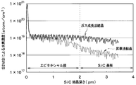
- FIG. 2 shows the results of examining the hydrogen concentration distribution of the SiC substrate 1 and the epitaxial film 2 by SIMS (abbreviation of Secondary Ion Mass Spectrometry) when these experiments were performed.
- SIMS abbreviation of Secondary Ion Mass Spectrometry
- the SiC substrate 1 having a low hydrogen concentration was manufactured by using the sublimation method, the hydrogen concentration gradually changed at the boundary position between the SiC substrate 1 and the epitaxial film 2. From this, it can be seen that hydrogen in the epitaxial film 2 is diffused into the SiC substrate 1. As described above, when the hydrogen concentration in the epitaxial film 2 is lowered, the carrier lifetime is shortened and the electrical resistance is increased, thereby deteriorating the characteristics of the SiC semiconductor device.
- a pn diode was prepared using a diode less than 1/10.
- the pn diode formed on the latter semiconductor substrate has a large electric resistance.
- the carrier lifetime depends on the hydrogen concentration in the epitaxial film 2, it is considered that the carrier concentration is shortened because the hydrogen concentration is lowered on the interface side of the epitaxial film 2 with the SiC substrate 1.
- the pn diode formed on the former semiconductor substrate had a smaller electric resistance than the pn diode formed on the latter semiconductor substrate. This is presumably because the reduction of the carrier lifetime was suppressed because the hydrogen concentration of the epitaxial film 2 did not decrease.
- the concentration ratio of the hydrogen concentration of epitaxial film 2 to the hydrogen concentration of SiC substrate 1 is 0.2 to 5, preferably 0.5 to 2. It is trying to become. Thereby, diffusion of hydrogen at the boundary position between epitaxial film 2 and SiC substrate 1 can be suppressed, and a semiconductor substrate capable of suppressing a decrease in hydrogen concentration can be obtained. Therefore, it is possible to improve the characteristics of a SiC semiconductor device formed using a semiconductor substrate, for example, a bipolar device such as a pn diode.
- the SiC substrate 1 is manufactured by the gas growth method in which the hydrogen concentration is easily increased has been described.
- other methods may be used as long as the SiC substrate 1 having a desired hydrogen concentration can be manufactured.
- the SiC substrate 1 having a hydrogen concentration of 5 ⁇ 10 16 cm ⁇ 3 or more can be manufactured. While using the SiC substrate 1 manufactured in this way, the concentration ratio of the hydrogen concentration of the epitaxial film 2 to the hydrogen concentration of the SiC substrate 1 is 0.2 to 5, preferably 0.5 to 2. The same effect as the first embodiment can be obtained. Also in that case, the SiC substrate 1 can be made into a desired conductivity type by introducing a raw material containing nitrogen as an N-type dopant and aluminum as a P-type dopant into the SiC substrate 1.
Landscapes
- Chemical & Material Sciences (AREA)
- Engineering & Computer Science (AREA)
- Materials Engineering (AREA)
- Metallurgy (AREA)
- Organic Chemistry (AREA)
- Crystallography & Structural Chemistry (AREA)
- Chemical Kinetics & Catalysis (AREA)
- General Chemical & Material Sciences (AREA)
- Inorganic Chemistry (AREA)
- Mechanical Engineering (AREA)
- Crystals, And After-Treatments Of Crystals (AREA)
- Recrystallisation Techniques (AREA)
Abstract
SiC基板(1)およびエピタキシャル膜(2)を有する半導体基板において、SiC基板(1)の水素濃度に対するエピタキシャル膜(2)の水素濃度の濃度比が0.2~5、好ましくは0.5~2となるようにする。これにより、エピタキシャル膜(2)とSiC基板(1)との境界位置における水素の拡散を抑制でき、水素濃度の低下が抑制できる半導体基板とすることが可能となる。したがって、半導体基板を用いて形成されるSiC半導体デバイス、例えばpnダイオードなどのバイポーラデバイスの特性の向上を図ることが可能となる。
Description
本出願は、2016年3月4日に出願された日本特許出願番号2016-42451号に基づくもので、ここにその記載内容が参照により組み入れられる。
本開示は、炭化珪素(以下、SiCという)にて構成されたSiC基板の上にSiCにて構成されたエピタキシャル膜が形成されてなる半導体基板およびその製造方法に関するものである。
従来より、SiCにて構成される半導体基板として、SiC基板の上にSiCにて構成されたエピタキシャル膜が形成されたものがある。SiCにて構成される半導体基板は、SiC半導体デバイスとして、例えばpnダイオードやバイポーラトランジスタの形成に用いられる。
このような半導体基板は、アルゴン雰囲気下で昇華法によって結晶成長させたSiC基板を用いて、水素をキャリアとしたCVD(chemical vapordepositionの略)法により、SiC基板の表面にエピタキシャル膜を成長させることによって形成される。
また、SiC基板の成長を昇華法にて行う場合に、昇華法の成長チャンバー内に水素を導入することによって成長結晶中への窒素の取り込みを防止すれば、超高純度のSiC単結晶を得ることが可能となり、半絶縁性の結晶を作成することもできる(特許文献1参照)。
SiC半導体デバイスにおけるキャリアライフタイムが結晶中の水素濃度に依存する。このため、SiC基板の上にSiCにて構成されたエピタキシャル膜を構成する場合、エピタキシャル膜を成長させる際にキャリアとして水素を用いて水素が導入されるようにすると、エピタキシャル膜中のキャリアライフタイムが長くなる。
しかしながら、水素濃度レベルの低いSiC基板の上にエピタキシャル膜を構成する場合、図3に示すように、水素濃度レベルの高いエピタキシャル膜側から水素濃度レベルの低いSiC基板側へ水素が拡散してしまうことが確認された。このため、SiC基板とエピタキシャル膜との界面において、エピタキシャル膜中の水素濃度が低下し、それに起因してキャリアライフタイムが短くなって、電気抵抗が大きくなるなど、SiC半導体デバイスの特性を悪化させるという課題が生じる。
上記した特許文献1のように、SiC基板の成長を昇華法にて行う場合において、成長チャンバー内に水素を導入すれば、SiC基板中に水素が導入され得る。ところが、水素濃度の差によってエピタキシャル膜からSiC基板側への水素の拡散が起こるため、単にSiC基板中に水素が導入されただけでは水素の拡散を抑制できない。よって、上記問題が発生する。
本開示は、SiCにて構成されたエピタキシャル膜からSiC基板側への水素の拡散を抑制でき、SiC半導体デバイスの特性の向上を図ることが可能な半導体基板およびその製造方法を提供することを目的とする。
本開示の1つの観点における半導体基板は、SiC単結晶にて構成され、水素を含むSiC基板と、SiC基板の上に形成され、水素を含むエピタキシャル膜と、を有し、SiC基板の水素濃度に対するエピタキシャル膜の水素濃度の濃度比が0.2~5とされている。
このように、SiC基板およびエピタキシャル膜を有する半導体基板において、SiC基板の水素濃度に対するエピタキシャル膜の水素濃度の濃度比が0.2~5となるようにしている。これにより、エピタキシャル膜とSiC基板との界面における水素の拡散を抑制でき、エピタキシャル膜の水素濃度の低下が抑制できる半導体基板とすることが可能となる。したがって、半導体基板を用いて形成されるSiC半導体デバイス、例えばバイポーラデバイスの特性の向上を図ることが可能となる。
本開示のもう1つの観点における半導体基板の製造方法は、Si含有ガスとC含有ガスから炭化珪素を合成するガス成長法にて、水素をキャリアガスとして用いることで水素を含有する炭化珪素単結晶を形成し、該炭化珪素単結晶にて炭化珪素基板を製造することと、炭化珪素基板の上に、水素をキャリアガスとして用いることで水素を含むエピタキシャル膜を形成することと、を含み、炭化珪素基板を製造することおよびエピタキシャル膜を形成することにおいては、炭化珪素基板の水素濃度に対するエピタキシャル膜の水素濃度の濃度比を0.2~5としている。
このように、ガス成長法を用いてSiC基板を製造するためのSiCインゴットを形成すると、昇華法を用いる場合と比較して、水素濃度を高くしやすくなる。このため、ガス成長法を用いてSiC基板を形成すると、SiC基板の水素濃度に対するエピタキシャル膜の水素濃度の濃度比を0.2~5に設定し易く、好適である。
以下、本開示の実施形態について図に基づいて説明する。なお、以下の各実施形態相互において、互いに同一もしくは均等である部分には、同一符号を付して説明を行う。
(第1実施形態)
第1実施形態について説明する。図1に示すように、本実施形態にかかる半導体基板は、SiC基板1の上にSiCにて構成されるエピタキシャル膜2を成長させたものである。
第1実施形態について説明する。図1に示すように、本実施形態にかかる半導体基板は、SiC基板1の上にSiCにて構成されるエピタキシャル膜2を成長させたものである。
SiC基板1は、n型不純物である窒素等もしくはp型不純物であるアルミニウム等がドーピングされることでn型SiCもしくはp型SiCとされている。また、SiC基板1には水素がドーピングされており、例えば水素濃度が2×10¹⁸~5×1019cm-3とされている。水素濃度については任意であるが、半導体基板を使用して形成するSiC半導体デバイスにおいて、所望のキャリアライフタイムを得るために必要な濃度に設定するのが好ましい。上記したように、水素濃度が少なくとも2×10¹⁸~5×1019cm-3とされていれば、所望のキャリアライフタイムを得ることができる。
エピタキシャル膜2は、SiC基板1の表面にCVD法によってエピタキシャル成長させられた膜である。このエピタキシャル膜2も、例えばn型不純物である窒素等もしくはp型不純物であるアルミニウム等がドーピングされることでn型SiCもしくはp型SiCとされている。また、エピタキシャル膜2にも水素がドーピングされており、SiC基板1の水素濃度に対するエピタキシャル膜2の水素濃度の濃度比が0.2~5、好ましくは0.5~2とされている。
SiC基板1やエピタキシャル膜2の導電型については任意であり、形成するSiC半導体デバイスに応じて決められる。例えば、SiC半導体デバイスとしてpnダイオードを形成する場合には、SiC基板1をn型SiCで構成し、エピタキシャル膜2をp型SiCで構成する。
SiC基板1の水素濃度とエピタキシャル膜2の水素濃度とに差があると、水素濃度が高い方側から低い方側への水素の拡散が発生し、特に1桁以上濃度が異なってくるとその拡散が顕著になることを確認している。この拡散を抑制できる範囲について検討を行ったところ、水素濃度の高い方に対して低い方の濃度が1/5の値となるまでは拡散抑制効果が得られ、それ以上になると拡散抑制効果が得られなくなるという結果が得られた。そして、SiC基板1の水素濃度とエピタキシャル膜2の水素濃度が近いほど、水素の拡散を抑制することが可能となり、より好ましくは水素濃度の高い方に対して低い方の濃度が半分以上の値になると拡散抑制効果がより高くなるという結果が得られた。このため、上記したように、SiC基板1の水素濃度に対するエピタキシャル膜2の水素濃度の濃度比が0.2~5となるようにしており、好ましくは0.5~2となるようにしている。
このように構成された半導体基板は、SiC半導体デバイスの形成に用いられる。例えば、SiC半導体デバイスとしてはpnダイオードなどのバイポーラ素子が挙げられる。
このようなpnダイオードにおいて、SiC基板1の水素濃度に対するエピタキシャル膜2の水素濃度の濃度比が上記した値とされていることから、エピタキシャル膜2中の水素の拡散が抑制される。このため、キャリアライフタイムが短くなることを抑制でき、電気抵抗が大きくなることなどが抑制できる。したがって、SiC半導体デバイスの特性悪化を抑制できる。同様の効果は、IGBT(Insulated GateBipolarTransistorの略)等のバイポーラトランジスタにおいても期待できる。
続いて、上記のように構成される半導体基板の製造方法について説明する。
まず、SiC基板1を製造する。具体的には、ガス成長法によってSiC基板1を形成するためのSiCインゴットを形成し、SiCインゴットをスライスすることによってSiC基板1を製造する。
例えば、図示しないが、台座上に種結晶となるSiC単結晶基板を配置し、SiC単結晶基板に対して例えばシラン(SiH4)などのSi含有ガスと例えばプロパン(C3H8)などのC含有ガスを含む混合ガスをSiC原料ガスとして供給する。また、ガス成長が行われる成長空間を2300~2500℃程度に加熱する。これにより、SiC単結晶基板の表面にSiC単結晶にて構成されるSiCインゴットを成長させることができる。
そして、このSiCインゴットの成長の際に、Si含有ガスとC含有ガスのキャリアガスとして水素を導入し、SiCインゴット中に水素がドープされるようにしている。このときの水素のドープ量は、SiC単結晶基板に供給されるガス雰囲気中における水素の分圧によって決まる。水素の分圧は、キャリアガスとして導入する水素の量などによって決まり、本実施形態のようにSi含有ガスやC含有ガス中に水素元素が含まれている場合には、これらに含まれる水素の量とキャリアガスとして導入する水素の総量によって決まる。このため、導入する水素の量を調整し、エピタキシャル膜2中に導入されるライフタイム制御のために好適な水素濃度を加味した上で、SiC基板1の水素濃度に対するエピタキシャル膜2の水素濃度の濃度比が上記値となるようにしている。
例えば、ガス成長法によってSiCインゴットを製造する場合には、Si:Hが1:10程度となるようにすると、SiC基板1の水素濃度に対するエピタキシャル膜2の水素濃度の濃度比が上記値に含まれるようにSiCインゴット中の水素濃度を設定できる。実験により、このような比率で水素の導入量を調整したところ、SiC基板1の水素濃度は1×1019cm-3となった。したがって、SiC原料ガスとなるSi含有ガスやC含有ガスとしてシランやプロパンを用いる場合、SiC原料ガス中に含まれる水素元素の量とキャリアガスとなる水素の導入量とを足した量が、上記比率に即した量となるように水素の導入量を決めればよい。
このようにして得られるSiCインゴットをスライスすることでSiC基板1を製造した後、図示しない化学気相成長(以下、CVD(chemical vapordepositionの略)という)装置内にSiC基板1を配置する。そして、CVD装置を用いて、SiC基板1の一面にCVD法にてエピタキシャル膜2を成長させる。CVD法では、キャリアガスとして水素を用いており、エピタキシャル膜2の成長中に水素がドーピングされる。具体的には、水素をキャリアガスとして、例えばシランなどのSi含有ガスと例えばプロパンなどのC含有ガスとをCVD装置内に導入し、1500~1600℃の温度でエピタキシャル膜2を成長させることができる。
このとき、キャリアガスとして導入する水素の導入量を調整し、ガス雰囲気中における水素の分圧を調整することで、エピタキシャル膜2中における水素濃度が上記値となるようにする。すなわち、SiC基板1の水素濃度に対するエピタキシャル膜2の水素濃度の濃度比が0.2~5となるようにしており、好ましくは0.5~2となるようにしている。このようにエピタキシャル膜2の水素濃度を設定することで、SiC基板1中からエピタキシャル膜2中へ、もしくは、その逆方向への水素の拡散を抑制できる。
実験により、ガス成長法によって水素濃度が1×1019cm-3となるSiC基板1を製造した場合において、エピタキシャル膜2の水素濃度も1×1019cm-3となるようにエピタキシャル膜2を形成した場合の水素濃度分布について調べた。また、参考として、昇華法によってSiC基板1を製造した場合において、そのSiC基板1の上にエピタキシャル膜2を形成した場合の水素濃度分布について調べた。昇華法は、黒鉛製坩堝内にSiC原料を配置すると共に台座上にSiC単結晶基板を配置し、2200~2400℃で昇華させたSiC原料ガスをそれより数十~数百℃低温としたSiC単結晶基板に供給してSiC単結晶インゴットを成長させる手法である。昇華法ではアルゴン(Ar)雰囲気中においてSiC原料を加熱昇華させるため、SiC単結晶インゴット中に水素が殆どドーピングされない。昇華法によって形成した場合、SiC基板1の水素濃度は1×1018cm-3未満となり、ライフタイム制御の為に水素がドーピングされるエピタキシャル膜2の水素濃度に対して1桁以上少ない濃度となる。
これらの実験を行った場合において、SIMS(Secondary Ion Mass Spectrometryの略)測定によってSiC基板1およびエピタキシャル膜2の水素濃度分布を調べた結果を図2に示す。
この図に示すように、昇華法を用いて水素濃度が低いSiC基板1を製造した場合には、SiC基板1とエピタキシャル膜2との境界位置において水素濃度が緩やかに変化していた。このことから、エピタキシャル膜2中の水素がSiC基板1中へ拡散していることが判る。このように、エピタキシャル膜2中における水素濃度が低下してしまうと、キャリアライフタイムが短くなり、電気抵抗が大きくなるなど、SiC半導体デバイスの特性悪化が生じることとなる。
一方、ガス成長法を用いてSiC基板1の水素濃度をエピタキシャル膜2の水素濃度に近づけた場合には、SiC基板1の水素濃度とエピタキシャル膜2の水素濃度の変化が見られなかった。このことから、SiC基板1中からエピタキシャル膜2中へ、もしくは、その逆方向への水素の拡散を抑制できていることが判る。これにより、キャリアライフタイムが短くなることを抑制でき、電気抵抗が大きくなることなどが抑制できる。したがって、SiC半導体デバイスの特性悪化を抑制できる。
図2の実験で製造した半導体基板、つまりSiC基板1の水素濃度に対するエピタキシャル膜2の水素濃度の濃度比が0.2~5のものと、SiC基板1の水素濃度がエピタキシャル膜2の水素濃度の1/10未満のものを用いて、pnダイオードを作成した。
その結果、後者の半導体基板に形成したpnダイオードにおいては、電気抵抗が大きい値となった。キャリアライフタイムがエピタキシャル膜2中における水素濃度に依存しているが、エピタキシャル膜2のうちのSiC基板1との界面側において水素濃度が低くなって、キャリアライフタイムが短くなったためと考えられる。
これに対して、前者の半導体基板に形成したpnダイオードおいては、後者の半導体基板に形成したpnダイオードと比較して、電気抵抗が小さな値となった。これは、エピタキシャル膜2の水素濃度の低下が生じていないために、キャリアライフタイムが短くなることが抑制されたためと考えられる。
以上説明したように、SiC基板1およびエピタキシャル膜2を有する半導体基板において、SiC基板1の水素濃度に対するエピタキシャル膜2の水素濃度の濃度比が0.2~5、好ましくは0.5~2となるようにしている。これにより、エピタキシャル膜2とSiC基板1との境界位置における水素の拡散を抑制でき、水素濃度の低下が抑制できる半導体基板とすることが可能となる。したがって、半導体基板を用いて形成されるSiC半導体デバイス、例えばpnダイオードなどのバイポーラデバイスの特性の向上を図ることが可能となる。
このような半導体基板の製造方法については任意であるが、上記したように、ガス成長法を用いてSiC基板1を製造するためのSiCインゴットを形成すると、昇華法を用いる場合と比較して、水素濃度を高くしやすくなる。このため、ガス成長法を用いてSiC基板1を形成すると、SiC基板1とエピタキシャル膜2の水素濃度比を上記した値に設定し易く、好適である。
(他の実施形態)
本開示は、上記した実施形態に準拠して記述されたが、当該実施形態に限定されるものではなく、様々な変形例や均等範囲内の変形をも包含する。加えて、様々な組み合わせや形態、さらには、それらに一要素のみ、それ以上、あるいはそれ以下、を含む他の組み合わせや形態をも、本開示の範疇や思想範囲に入るものである。
本開示は、上記した実施形態に準拠して記述されたが、当該実施形態に限定されるものではなく、様々な変形例や均等範囲内の変形をも包含する。加えて、様々な組み合わせや形態、さらには、それらに一要素のみ、それ以上、あるいはそれ以下、を含む他の組み合わせや形態をも、本開示の範疇や思想範囲に入るものである。
上記第1実施形態では、SiC基板1を水素濃度が高くしやすいガス成長法によって製造する場合について説明したが、所望の水素濃度のSiC基板1を製造できれば他の方法であっても良い。
例えば、昇華法において、結晶成長の工程中に水素を導入するようにすれば、5×1016cm-3以上の水素濃度となるSiC基板1を製造することもできる。このように製造されるSiC基板1を用いつつ、SiC基板1の水素濃度に対するエピタキシャル膜2の水素濃度の濃度比が0.2~5、好ましくは0.5~2となるようにすれば、第1実施形態と同様の効果が得られる。その場合にも、SiC基板1に対してN型ドーパントとなる窒素やP型ドーパントとなるアルミニウムを含む原料を導入することで、SiC基板1を所望の導電型にすることができる。
Claims (6)
- 炭化珪素単結晶にて構成され、水素を含む炭化珪素基板(1)と、
前記炭化珪素基板の上に形成され、水素を含むエピタキシャル膜(2)と、を有し、
前記炭化珪素基板の水素濃度に対する前記エピタキシャル膜の水素濃度の濃度比が0.2~5とされている半導体基板。 - 前記炭化珪素基板の水素濃度に対する前記エピタキシャル膜の水素濃度の濃度比が0.5~2とされている請求項1に記載の半導体基板。
- 前記炭化珪素基板の水素濃度が2×10¹⁸~5×1019cm-3である請求項1または2に記載の半導体基板。
- Si含有ガスとC含有ガスから炭化珪素を合成するガス成長法にて、水素をキャリアガスとして用いることで水素を含有する炭化珪素単結晶を形成し、該炭化珪素単結晶にて炭化珪素基板(1)を製造することと、
前記炭化珪素基板の上に、水素をキャリアガスとして用いることで水素を含むエピタキシャル膜(2)を形成することと、を含み、
前記炭化珪素基板を製造することおよび前記エピタキシャル膜を形成することにおいては、前記炭化珪素基板の水素濃度に対する前記エピタキシャル膜の水素濃度の濃度比を0.2~5とする半導体基板の製造方法。 - 前記炭化珪素基板を製造することおよび前記エピタキシャル膜を形成することにおいては、前記炭化珪素基板の水素濃度に対する前記エピタキシャル膜の水素濃度の濃度比を0.5~2とする請求項4に記載の半導体基板の製造方法。
- 前記炭化珪素基板を製造することにおいては、前記炭化珪素基板の水素濃度を2×10¹⁸~5×1019cm-3とする請求項4または5に記載の半導体基板の製造方法。
Priority Applications (3)
| Application Number | Priority Date | Filing Date | Title |
|---|---|---|---|
| US16/075,782 US10490635B2 (en) | 2016-03-04 | 2017-01-12 | Semiconductor substrate made of silicon carbide and method for manufacturing same |
| CN201780014638.2A CN108699726B (zh) | 2016-03-04 | 2017-01-12 | 由碳化硅构成的半导体基板及其制造方法 |
| DE112017001142.6T DE112017001142B4 (de) | 2016-03-04 | 2017-01-12 | Herstellungsverfahren eines Halbleitersubstrats aus Siliziumcarbid und mit diesem Verfahren herstellbares Halbleitersubstrat |
Applications Claiming Priority (2)
| Application Number | Priority Date | Filing Date | Title |
|---|---|---|---|
| JP2016042451A JP6578994B2 (ja) | 2016-03-04 | 2016-03-04 | 炭化珪素にて構成される半導体基板およびその製造方法 |
| JP2016-042451 | 2016-03-04 |
Publications (1)
| Publication Number | Publication Date |
|---|---|
| WO2017149945A1 true WO2017149945A1 (ja) | 2017-09-08 |
Family
ID=59743616
Family Applications (1)
| Application Number | Title | Priority Date | Filing Date |
|---|---|---|---|
| PCT/JP2017/000802 Ceased WO2017149945A1 (ja) | 2016-03-04 | 2017-01-12 | 炭化珪素にて構成される半導体基板およびその製造方法 |
Country Status (5)
| Country | Link |
|---|---|
| US (1) | US10490635B2 (ja) |
| JP (1) | JP6578994B2 (ja) |
| CN (1) | CN108699726B (ja) |
| DE (1) | DE112017001142B4 (ja) |
| WO (1) | WO2017149945A1 (ja) |
Families Citing this family (1)
| Publication number | Priority date | Publication date | Assignee | Title |
|---|---|---|---|---|
| JP7331590B2 (ja) * | 2019-09-27 | 2023-08-23 | 株式会社デンソー | 炭化珪素半導体装置 |
Citations (5)
| Publication number | Priority date | Publication date | Assignee | Title |
|---|---|---|---|---|
| JP2007246350A (ja) * | 2006-03-16 | 2007-09-27 | Mitsubishi Materials Corp | SiC基板の製造方法及びSiC基板並びに半導体装置 |
| JP2008214146A (ja) * | 2007-03-06 | 2008-09-18 | Denso Corp | 炭化珪素単結晶の製造装置および製造方法 |
| JP2013014469A (ja) * | 2011-07-04 | 2013-01-24 | Panasonic Corp | SiCエピタキシャル基板およびその製造方法 |
| JP2015002207A (ja) * | 2013-06-13 | 2015-01-05 | 昭和電工株式会社 | SiCエピタキシャルウェハ及びその製造方法 |
| JP2015093810A (ja) * | 2013-11-12 | 2015-05-18 | 一般財団法人電力中央研究所 | 炭化珪素単結晶の製造方法及び炭化珪素単結晶の製造装置 |
Family Cites Families (8)
| Publication number | Priority date | Publication date | Assignee | Title |
|---|---|---|---|---|
| JPS4891767A (ja) | 1972-03-06 | 1973-11-29 | ||
| JPS609658B2 (ja) * | 1978-06-20 | 1985-03-12 | シヤープ株式会社 | 炭化珪素基板の製造方法 |
| EP1306890A2 (en) * | 2001-10-25 | 2003-05-02 | Matsushita Electric Industrial Co., Ltd. | Semiconductor substrate and device comprising SiC and method for fabricating the same |
| US7147715B2 (en) | 2003-07-28 | 2006-12-12 | Cree, Inc. | Growth of ultra-high purity silicon carbide crystals in an ambient containing hydrogen |
| US7601441B2 (en) | 2002-06-24 | 2009-10-13 | Cree, Inc. | One hundred millimeter high purity semi-insulating single crystal silicon carbide wafer |
| US7070542B2 (en) * | 2002-07-26 | 2006-07-04 | Unisen, Inc. | Exercise machine including weight measurement system |
| JP2007096263A (ja) * | 2005-08-31 | 2007-04-12 | Denso Corp | 炭化珪素半導体装置およびその製造方法。 |
| JP2012051760A (ja) | 2010-09-01 | 2012-03-15 | Bridgestone Corp | 炭化ケイ素単結晶の製造方法 |
-
2016
- 2016-03-04 JP JP2016042451A patent/JP6578994B2/ja active Active
-
2017
- 2017-01-12 DE DE112017001142.6T patent/DE112017001142B4/de active Active
- 2017-01-12 WO PCT/JP2017/000802 patent/WO2017149945A1/ja not_active Ceased
- 2017-01-12 US US16/075,782 patent/US10490635B2/en active Active
- 2017-01-12 CN CN201780014638.2A patent/CN108699726B/zh active Active
Patent Citations (5)
| Publication number | Priority date | Publication date | Assignee | Title |
|---|---|---|---|---|
| JP2007246350A (ja) * | 2006-03-16 | 2007-09-27 | Mitsubishi Materials Corp | SiC基板の製造方法及びSiC基板並びに半導体装置 |
| JP2008214146A (ja) * | 2007-03-06 | 2008-09-18 | Denso Corp | 炭化珪素単結晶の製造装置および製造方法 |
| JP2013014469A (ja) * | 2011-07-04 | 2013-01-24 | Panasonic Corp | SiCエピタキシャル基板およびその製造方法 |
| JP2015002207A (ja) * | 2013-06-13 | 2015-01-05 | 昭和電工株式会社 | SiCエピタキシャルウェハ及びその製造方法 |
| JP2015093810A (ja) * | 2013-11-12 | 2015-05-18 | 一般財団法人電力中央研究所 | 炭化珪素単結晶の製造方法及び炭化珪素単結晶の製造装置 |
Also Published As
| Publication number | Publication date |
|---|---|
| JP6578994B2 (ja) | 2019-09-25 |
| JP2017154955A (ja) | 2017-09-07 |
| US10490635B2 (en) | 2019-11-26 |
| CN108699726B (zh) | 2021-05-14 |
| CN108699726A (zh) | 2018-10-23 |
| US20190035894A1 (en) | 2019-01-31 |
| DE112017001142T5 (de) | 2018-11-22 |
| DE112017001142B4 (de) | 2023-06-29 |
Similar Documents
| Publication | Publication Date | Title |
|---|---|---|
| US11982016B2 (en) | Method for growing beta-Ga2O3-based single crystal film, and crystalline layered structure | |
| US10026610B2 (en) | Silicon carbide semiconductor device manufacturing method | |
| JP7647791B2 (ja) | SiCエピタキシャルウェハ | |
| CN104885197B (zh) | 制造碳化硅半导体衬底的方法以及制造碳化硅半导体器件的方法 | |
| US9873954B2 (en) | Epitaxial wafer and method for fabricating the same | |
| US20180053649A1 (en) | Method to grow a semi-conducting sic layer | |
| US11183385B2 (en) | Method for passivating silicon carbide epitaxial layer | |
| EP3141635B1 (en) | Semiconductor substrate, epitaxial wafer, and method for manufacturing epitaxial wafer | |
| US20200071849A1 (en) | n-TYPE 4H-SiC SINGLE CRYSTAL SUBSTRATE AND METHOD OF PRODUCING n-TYPE 4H-SiC SINGLE CRYSTAL SUBSTRATE | |
| JP7127283B2 (ja) | 炭化珪素半導体基板および炭化珪素半導体基板の製造方法 | |
| JP2016096247A (ja) | 半導体基板およびその製造方法 | |
| JP6578994B2 (ja) | 炭化珪素にて構成される半導体基板およびその製造方法 | |
| JP2014103363A (ja) | 炭化珪素半導体基板の製造方法 | |
| De Boer et al. | Selective versus non-selective growth of Si and SiGe | |
| JP2004343133A (ja) | 炭化珪素製造方法、炭化珪素及び半導体装置 | |
| CN119278499A (zh) | 半导体晶圆的制造方法及半导体晶圆 | |
| CN113913931A (zh) | 一种具有p型缓冲层的外延结构及其制备方法 | |
| KR102474331B1 (ko) | 에피택셜 웨이퍼 및 그 제조 방법 | |
| WO2020045172A1 (ja) | エピタキシャル基板 | |
| JP7441794B2 (ja) | 核生成層の堆積方法 | |
| Tanaka et al. | Study on N and B doping by closed sublimation growth using separated Ta crucible | |
| CN103348445B (zh) | 用于拉伸应变应用上的高拉伸硅合金的外延法 | |
| JP2014154587A (ja) | 炭化珪素半導体基板の製造方法および炭化珪素半導体装置の製造方法 | |
| CN103348445A (zh) | 用于拉伸应变应用上的高拉伸硅合金的外延法 |
Legal Events
| Date | Code | Title | Description |
|---|---|---|---|
| 121 | Ep: the epo has been informed by wipo that ep was designated in this application |
Ref document number: 17759417 Country of ref document: EP Kind code of ref document: A1 |
|
| 122 | Ep: pct application non-entry in european phase |
Ref document number: 17759417 Country of ref document: EP Kind code of ref document: A1 |