WO2017135071A1 - 電力変換装置 - Google Patents
電力変換装置 Download PDFInfo
- Publication number
- WO2017135071A1 WO2017135071A1 PCT/JP2017/001909 JP2017001909W WO2017135071A1 WO 2017135071 A1 WO2017135071 A1 WO 2017135071A1 JP 2017001909 W JP2017001909 W JP 2017001909W WO 2017135071 A1 WO2017135071 A1 WO 2017135071A1
- Authority
- WO
- WIPO (PCT)
- Prior art keywords
- electronic circuit
- circuit board
- fixing
- case
- fixed
- Prior art date
Links
Images

Classifications
-
- H—ELECTRICITY
- H05—ELECTRIC TECHNIQUES NOT OTHERWISE PROVIDED FOR
- H05K—PRINTED CIRCUITS; CASINGS OR CONSTRUCTIONAL DETAILS OF ELECTRIC APPARATUS; MANUFACTURE OF ASSEMBLAGES OF ELECTRICAL COMPONENTS
- H05K7/00—Constructional details common to different types of electric apparatus
- H05K7/14—Mounting supporting structure in casing or on frame or rack
- H05K7/1422—Printed circuit boards receptacles, e.g. stacked structures, electronic circuit modules or box like frames
- H05K7/1427—Housings
- H05K7/1432—Housings specially adapted for power drive units or power converters
-
- B—PERFORMING OPERATIONS; TRANSPORTING
- B60—VEHICLES IN GENERAL
- B60L—PROPULSION OF ELECTRICALLY-PROPELLED VEHICLES; SUPPLYING ELECTRIC POWER FOR AUXILIARY EQUIPMENT OF ELECTRICALLY-PROPELLED VEHICLES; ELECTRODYNAMIC BRAKE SYSTEMS FOR VEHICLES IN GENERAL; MAGNETIC SUSPENSION OR LEVITATION FOR VEHICLES; MONITORING OPERATING VARIABLES OF ELECTRICALLY-PROPELLED VEHICLES; ELECTRIC SAFETY DEVICES FOR ELECTRICALLY-PROPELLED VEHICLES
- B60L50/00—Electric propulsion with power supplied within the vehicle
- B60L50/50—Electric propulsion with power supplied within the vehicle using propulsion power supplied by batteries or fuel cells
- B60L50/51—Electric propulsion with power supplied within the vehicle using propulsion power supplied by batteries or fuel cells characterised by AC-motors
-
- H—ELECTRICITY
- H02—GENERATION; CONVERSION OR DISTRIBUTION OF ELECTRIC POWER
- H02M—APPARATUS FOR CONVERSION BETWEEN AC AND AC, BETWEEN AC AND DC, OR BETWEEN DC AND DC, AND FOR USE WITH MAINS OR SIMILAR POWER SUPPLY SYSTEMS; CONVERSION OF DC OR AC INPUT POWER INTO SURGE OUTPUT POWER; CONTROL OR REGULATION THEREOF
- H02M7/00—Conversion of ac power input into dc power output; Conversion of dc power input into ac power output
- H02M7/003—Constructional details, e.g. physical layout, assembly, wiring or busbar connections
-
- H—ELECTRICITY
- H02—GENERATION; CONVERSION OR DISTRIBUTION OF ELECTRIC POWER
- H02M—APPARATUS FOR CONVERSION BETWEEN AC AND AC, BETWEEN AC AND DC, OR BETWEEN DC AND DC, AND FOR USE WITH MAINS OR SIMILAR POWER SUPPLY SYSTEMS; CONVERSION OF DC OR AC INPUT POWER INTO SURGE OUTPUT POWER; CONTROL OR REGULATION THEREOF
- H02M7/00—Conversion of ac power input into dc power output; Conversion of dc power input into ac power output
- H02M7/42—Conversion of dc power input into ac power output without possibility of reversal
- H02M7/44—Conversion of dc power input into ac power output without possibility of reversal by static converters
- H02M7/48—Conversion of dc power input into ac power output without possibility of reversal by static converters using discharge tubes with control electrode or semiconductor devices with control electrode
-
- H—ELECTRICITY
- H05—ELECTRIC TECHNIQUES NOT OTHERWISE PROVIDED FOR
- H05K—PRINTED CIRCUITS; CASINGS OR CONSTRUCTIONAL DETAILS OF ELECTRIC APPARATUS; MANUFACTURE OF ASSEMBLAGES OF ELECTRICAL COMPONENTS
- H05K1/00—Printed circuits
- H05K1/02—Details
- H05K1/14—Structural association of two or more printed circuits
- H05K1/144—Stacked arrangements of planar printed circuit boards
-
- H—ELECTRICITY
- H05—ELECTRIC TECHNIQUES NOT OTHERWISE PROVIDED FOR
- H05K—PRINTED CIRCUITS; CASINGS OR CONSTRUCTIONAL DETAILS OF ELECTRIC APPARATUS; MANUFACTURE OF ASSEMBLAGES OF ELECTRICAL COMPONENTS
- H05K5/00—Casings, cabinets or drawers for electric apparatus
- H05K5/02—Details
- H05K5/03—Covers
-
- H—ELECTRICITY
- H05—ELECTRIC TECHNIQUES NOT OTHERWISE PROVIDED FOR
- H05K—PRINTED CIRCUITS; CASINGS OR CONSTRUCTIONAL DETAILS OF ELECTRIC APPARATUS; MANUFACTURE OF ASSEMBLAGES OF ELECTRICAL COMPONENTS
- H05K7/00—Constructional details common to different types of electric apparatus
- H05K7/14—Mounting supporting structure in casing or on frame or rack
- H05K7/1417—Mounting supporting structure in casing or on frame or rack having securing means for mounting boards, plates or wiring boards
-
- H—ELECTRICITY
- H05—ELECTRIC TECHNIQUES NOT OTHERWISE PROVIDED FOR
- H05K—PRINTED CIRCUITS; CASINGS OR CONSTRUCTIONAL DETAILS OF ELECTRIC APPARATUS; MANUFACTURE OF ASSEMBLAGES OF ELECTRICAL COMPONENTS
- H05K7/00—Constructional details common to different types of electric apparatus
- H05K7/14—Mounting supporting structure in casing or on frame or rack
- H05K7/1422—Printed circuit boards receptacles, e.g. stacked structures, electronic circuit modules or box like frames
- H05K7/1427—Housings
- H05K7/1432—Housings specially adapted for power drive units or power converters
- H05K7/14322—Housings specially adapted for power drive units or power converters wherein the control and power circuits of a power converter are arranged within the same casing
-
- H—ELECTRICITY
- H05—ELECTRIC TECHNIQUES NOT OTHERWISE PROVIDED FOR
- H05K—PRINTED CIRCUITS; CASINGS OR CONSTRUCTIONAL DETAILS OF ELECTRIC APPARATUS; MANUFACTURE OF ASSEMBLAGES OF ELECTRICAL COMPONENTS
- H05K9/00—Screening of apparatus or components against electric or magnetic fields
- H05K9/0007—Casings
- H05K9/002—Casings with localised screening
- H05K9/0022—Casings with localised screening of components mounted on printed circuit boards [PCB]
- H05K9/0024—Shield cases mounted on a PCB, e.g. cans or caps or conformal shields
- H05K9/0026—Shield cases mounted on a PCB, e.g. cans or caps or conformal shields integrally formed from metal sheet
-
- H—ELECTRICITY
- H05—ELECTRIC TECHNIQUES NOT OTHERWISE PROVIDED FOR
- H05K—PRINTED CIRCUITS; CASINGS OR CONSTRUCTIONAL DETAILS OF ELECTRIC APPARATUS; MANUFACTURE OF ASSEMBLAGES OF ELECTRICAL COMPONENTS
- H05K2201/00—Indexing scheme relating to printed circuits covered by H05K1/00
- H05K2201/04—Assemblies of printed circuits
- H05K2201/042—Stacked spaced PCBs; Planar parts of folded flexible circuits having mounted components in between or spaced from each other
-
- H—ELECTRICITY
- H05—ELECTRIC TECHNIQUES NOT OTHERWISE PROVIDED FOR
- H05K—PRINTED CIRCUITS; CASINGS OR CONSTRUCTIONAL DETAILS OF ELECTRIC APPARATUS; MANUFACTURE OF ASSEMBLAGES OF ELECTRICAL COMPONENTS
- H05K2201/00—Indexing scheme relating to printed circuits covered by H05K1/00
- H05K2201/10—Details of components or other objects attached to or integrated in a printed circuit board
- H05K2201/10227—Other objects, e.g. metallic pieces
- H05K2201/10371—Shields or metal cases
-
- H—ELECTRICITY
- H05—ELECTRIC TECHNIQUES NOT OTHERWISE PROVIDED FOR
- H05K—PRINTED CIRCUITS; CASINGS OR CONSTRUCTIONAL DETAILS OF ELECTRIC APPARATUS; MANUFACTURE OF ASSEMBLAGES OF ELECTRICAL COMPONENTS
- H05K2201/00—Indexing scheme relating to printed circuits covered by H05K1/00
- H05K2201/20—Details of printed circuits not provided for in H05K2201/01 - H05K2201/10
- H05K2201/2036—Permanent spacer or stand-off in a printed circuit or printed circuit assembly
-
- Y—GENERAL TAGGING OF NEW TECHNOLOGICAL DEVELOPMENTS; GENERAL TAGGING OF CROSS-SECTIONAL TECHNOLOGIES SPANNING OVER SEVERAL SECTIONS OF THE IPC; TECHNICAL SUBJECTS COVERED BY FORMER USPC CROSS-REFERENCE ART COLLECTIONS [XRACs] AND DIGESTS
- Y02—TECHNOLOGIES OR APPLICATIONS FOR MITIGATION OR ADAPTATION AGAINST CLIMATE CHANGE
- Y02T—CLIMATE CHANGE MITIGATION TECHNOLOGIES RELATED TO TRANSPORTATION
- Y02T10/00—Road transport of goods or passengers
- Y02T10/60—Other road transportation technologies with climate change mitigation effect
- Y02T10/70—Energy storage systems for electromobility, e.g. batteries
Definitions
- the present disclosure relates to a power conversion device including a plurality of electronic circuit boards.
- Patent Document 1 discloses a power conversion device including a semiconductor module incorporating a semiconductor element and a plurality of electronic circuit boards.
- the plurality of electronic circuit boards includes a first electronic circuit board for a high voltage system and a second electronic circuit board for a low voltage system.
- the first electronic circuit board and the second electronic circuit board are fixed to a fixing surface of a container that houses the semiconductor module in a state where the first electronic circuit board and the second electronic circuit board are stacked and arranged with a space therebetween in the substrate thickness direction.
- Such a stacked arrangement is effective to keep the dimension in the direction along the plate surface of the electronic circuit board small.
- the first electronic circuit board is disposed between the fixed surface of the container and the second electronic circuit board.
- the number of the fixing portions cannot be increased because the first electronic circuit board becomes an obstacle.
- the fixing location of the second electronic circuit board is limited to only the four corners of the board.
- the fixing location of the second electronic circuit board is biased only to the outer peripheral portion of the second electronic circuit board. Therefore, the second electronic circuit board is easily deformed by an external force, and it is difficult to ensure a desired fixing strength that can withstand vibrations received from the vehicle side during vehicle travel.
- a semiconductor module containing a semiconductor element A first electronic circuit board and a second electronic circuit board that are both electrically connected to the semiconductor module and arranged in a stacked manner with a space in the substrate thickness direction, A housing for housing both the semiconductor module, the first electronic circuit board, and the second electronic circuit board;
- the container includes a first fixing portion to which the first electronic circuit board is fixed, and a second fixing portion to which the second electronic circuit board is fixed.
- the second electronic circuit board is not interposed between the first fixing part of the container and the first electronic circuit board in the substrate thickness direction, and the second of the container in the substrate thickness direction.
- the power converter is configured such that the first electronic circuit board is not interposed between the fixing portion and the second electronic circuit board.
- the first electronic circuit board can be fixed to the container without being obstructed by the second electronic circuit board.
- the second electronic circuit board can be fixed to the container without being obstructed by the first electronic circuit board.
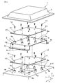
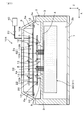
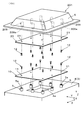
- FIG. 1 is a cross-sectional view illustrating a schematic structure of the power conversion device according to the first embodiment.
- FIG. 2 is a perspective view showing a fixing structure of each of the first electronic circuit board and the second electronic circuit board in the power conversion device in FIG.
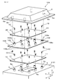
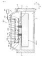
- FIG. 3 is a cross-sectional view illustrating a schematic structure of the power conversion device according to the second embodiment.
- FIG. 4 is a perspective view showing a fixing structure of each of the first electronic circuit board and the second electronic circuit board in the power conversion device in FIG.
- FIG. 5 is a cross-sectional view illustrating a schematic structure of the power conversion device according to the third embodiment.
- FIG. 6 is a perspective view showing a fixing structure of each of the first electronic circuit board and the second electronic circuit board in the power conversion device in FIG.
- the first direction that is the longitudinal direction of the semiconductor module is indicated by an arrow X
- the second direction that is the width direction of the semiconductor module is indicated by an arrow Y
- the first direction and A third direction orthogonal to both of the second directions is indicated by an arrow Z.
- the power conversion device 1 of Embodiment 1 includes a plurality of elements including a first electronic circuit board 10, a second electronic circuit board 20, and a semiconductor module 30. These plural elements are accommodated in an internal space partitioned by the container 2.
- the power conversion device 1 is mounted on, for example, an electric vehicle, a hybrid vehicle, or the like, and is used as an inverter that converts DC power supply power into AC power necessary for driving a drive motor.
- the container 2 includes a case 3, a cover 6 that closes the opening 3 a of the case 3, and a cover 7 that closes the opening 3 b of the case 3.
- the case 3 includes a partition wall 4 that partitions the internal space in the third direction Z.
- the partition wall 4 is provided with a plurality of boss portions (first fixing portions) 5 extending toward the first electronic circuit board 10 in order to fix the first electronic circuit board 10.
- the boss portion 5 is provided with a female screw portion 5a to which a male screw shaft of the screw 12 can be screwed.
- Both the case 3 and the covers 6 and 7 are made of an aluminum-based material mainly composed of aluminum.
- the semiconductor module 30 includes a semiconductor element 31 such as an IGBT that converts DC power to AC power.
- the semiconductor module 30 includes a plurality of control terminals 32 and power terminals (not shown).
- the first electronic circuit board 10 is a high-voltage electronic circuit board (also referred to as a “control circuit board”) having a rectangular shape in plan view and having a drive circuit for driving the semiconductor module 30 to be switched.
- the first electronic circuit board 10 is disposed closer to the semiconductor module 30 than the second electronic circuit board 20 in the third direction Z, which is the thickness direction of the board, and is electrically connected to the plurality of control terminals 32.
- the plurality of control terminals 32 extend from the semiconductor module 30 to the first electronic circuit board 10 through the openings 4 a provided in the partition wall 4 of the case 3. Accordingly, the first electronic circuit board 10 is electrically connected to the semiconductor module 30.
- the second electronic circuit board 20 is a low-voltage electronic circuit board having a rectangular shape having the same dimensions as the first electronic circuit board 10 in plan view and having a control circuit that controls the semiconductor module 30 based on vehicle information. is there.
- the second electronic circuit board 20 is electrically connected to the first electronic circuit board 10 by a conductive member 22 such as a terminal, and is electrically connected to a control unit (ECU) 40 on the vehicle side by a conductive member 23 such as a terminal. It is connected. Accordingly, the second electronic circuit board 20 is electrically connected to the semiconductor module 30.
- An input signal from the control unit 40 is transmitted to the semiconductor module 30 via the first electronic circuit board 10, the conductive member 22, and the second electronic circuit board 20.
- a detection signal such as a current output from the semiconductor module 30 is transmitted to the control unit 40 via the second electronic circuit board 20, the conductive member 22, and the first electronic circuit board 10.
- the first electronic circuit board 10 and the second electronic circuit board 20 are stacked in the third direction Z with a space 2a therebetween. Such an arrangement is effective in reducing the dimension in the direction along the substrate surface as compared with the case of using one electronic circuit board having the functions of these two electronic circuit boards 10 and 20.
- the inter-substrate plate 8 is a plate-like member including a flat plate portion 8a having a rectangular plan view and flange portions 8b provided on both sides in the first direction X of the flat plate portion 8a. Is fixed to the partition wall 4 of the case 3. In a state where the inter-substrate plate 8 is fixed to the partition wall 4, the inter-substrate plate 8 becomes a component of the container 2. In this case, it can be said that the container 2 has the inter-substrate plate 8.
- a plurality of fixing pins (second fixing portions) 9 for fixing the second electronic circuit board 20 are attached to the inter-substrate plate 8.
- the fixing pin 9 is attached to the inter-substrate plate 8 by being press-fitted into a through hole (not shown) provided in the flat plate portion 8 a of the inter-substrate plate 8.
- the fixing pin 9 includes a female screw portion 9a to which a male screw shaft of the screw 12 can be screwed.
- the inter-substrate plate 8 includes a plurality (two in FIG. 2) of insertion holes 8c formed through each flange portion 8b.
- the partition wall 4 includes a female screw portion 4b to which a male screw shaft of the screw 12 can be screwed.
- the inter-substrate plate 8 is configured to be fixed to the partition wall 4 by screwing the male screw shaft of the screw 12 inserted into each insertion hole 8 c into the female screw portion 4 b of the partition wall 4.
- a configuration is adopted in which a female screw portion such as a female screw portion 4b is provided on a boss portion extending from the partition wall 4 toward the inter-substrate plate 8, and the inter-substrate plate 8 is fixed to the boss portion. You can also
- the boss portion 5 is a constituent element of the container 2, and a plurality (eight in FIG. 2) are provided in the partition wall 4 so as to surround the opening 4a.
- a plurality of fixing pins 9 are provided on the flat plate portion 8a of the inter-substrate plate 8 almost without deviation.
- the fixing pin 9 is a constituent element of the container 2 in a state of being attached to the inter-substrate plate 8. Note that the arrangement and number of the boss portions 5 and the fixing pins 9 are not limited to those shown in FIG. 2 and can be variously changed as necessary.
- the first electronic circuit board 10 includes a plurality (eight in FIG. 2) of insertion holes 11 that are formed so as to penetrate in the third direction Z.
- the male screw shaft of the screw 12 inserted into each insertion hole 11 is connected to the female screw part 5 a of the boss part 5 in a state where each insertion hole 11 is aligned with the female screw part 5 a of the boss part 5. It is fixed to the boss portion 5 by screwing. As a result, the first electronic circuit board 10 is fixed to the case 3 of the container 2 while being supported by the plurality of boss portions 5.
- the second electronic circuit board 20 is not interposed between the boss portion 5 (component of the container 2) and the first electronic circuit board 10 in the third direction Z that is the board thickness direction. It is configured as follows. In other words, the boss portion 5 is located at a position where the second electronic circuit board 20 is not interposed between the boss part 5 and the first electronic circuit board 10 in the third direction Z (hereinafter also referred to as “first non-intervening position”). Is provided. This first non-intervening position can also be said to be a position where the fixing with the first electronic circuit board 10 is not disturbed by the second electronic circuit board 20.
- the second electronic circuit board 20 includes a plurality (eight in FIG. 2) of insertion holes 21 that are formed so as to penetrate in the third direction Z.
- the male screw shaft of the screw 12 inserted into each insertion hole 21 is connected to the female screw part 9 a of the fixing pin 9 with each insertion hole 21 aligned with the female screw part 9 a of the fixing pin 9.
- the fixing pin 9 is fixed by screwing.
- the second electronic circuit board 20 is fixed to the case 3 constituting the container 2 while being supported by the plurality of fixing pins 9 of the inter-substrate plate 8.
- the inter-substrate plate 8 fixed to the case 3 is provided with the fixing pin 9 (second fixing portion) for fixing the second electronic circuit board 20, and the container 2 Among them, a boss for fixing the first electronic circuit board 10 to a portion (partition wall 4 of the case 3) opposite to the second electronic circuit board 20 fixed to the inter-board plate 8 with the inter-board plate 8 interposed therebetween.
- a portion 5 (first fixing portion) is provided.
- a configuration in which the first electronic circuit board 10 is fixed to the fixing pin 9 and the second electronic circuit board 20 is fixed to the boss portion 5 may be employed.
- the first electronic circuit board 10 is not obstructed by the second electronic circuit board 20 by providing the boss portion 5 at the first non-intervening position.
- the case 3 can be fixed.
- the second electronic circuit board 20 can be fixed to the case 3 of the container 2 without being obstructed by the first electronic circuit board 10. it can.
- each of the first electronic circuit board 10 and the second electronic circuit board 20 is fixed to the container 2, the arrangement and the number of the fixing portions are not easily limited. Therefore, the number of fixing points of each electronic circuit board can be increased, and the fixing points can be prevented from being biased to, for example, only the four corners of each electronic circuit board. As a result, each electronic circuit board is not easily deformed by an external force, and a desired fixing strength that can withstand vibration received from the vehicle side when the vehicle travels can be secured.
- the boss part 5 cannot be provided in the part of the opening 4a in the partition wall 4. Accordingly, the surface of the first electronic circuit board 10 facing the opening 4a is not supported by the boss portion 5, but is instead supported by a plurality of control terminals 32 arranged in the opening 4a. Thereby, the fall of the fixed strength of the 1st electronic circuit board 10 is controlled.
- the arrangement of the fixing pin 9 in the flat plate portion 8a of the inter-substrate plate 8 is not limited (for example, the fixing pin 9 can be arranged in the central portion of the flat plate portion 8a). The fixing strength of the substrate 20 can be increased.
- the linear expansion coefficient of the inter-substrate plate 8 interposed between the case 3 and the first electronic circuit board 10 is an intermediate value between the linear expansion coefficient of the case 3 and the linear expansion coefficient of the first electronic circuit board 10. Therefore, the influence of thermal strain between these components can be reduced.
- the power conversion device 101 of the second embodiment is different from the power conversion device 1 of the first embodiment in the fixing structure of the second electronic circuit board 20.
- Other configurations are the same as those of the first embodiment. Therefore, only elements related to the fixing structure of the second electronic circuit board 20 will be described with reference to FIGS. 3 and 4 and description of other elements will be omitted. In these drawings, the same elements as those shown in FIGS. 1 and 2 are denoted by the same reference numerals.
- an inter-substrate plate 108 is interposed between the first electronic circuit board 10 and the second electronic circuit board 20 as an interposing member.
- the inter-substrate plate 108 is a plate-like member configured to have a rectangular shape in plan view and to have a size in plan view that exceeds both the first electronic circuit board 10 and the second electronic circuit board 20.
- the cover 6 includes a plurality of boss portions 6 a that extend toward the inter-substrate plate 108.
- the inter-substrate plate 108 is a flat member and is fixed to the boss 6 a of the cover 6 using screws 12.
- the inter-substrate plate 108 In the state where the inter-substrate plate 108 is fixed to the boss 6 a of the cover 6, the inter-substrate plate 108 becomes a constituent element of the container 2. In this case, it can be said that the container 2 has the inter-substrate plate 108.
- the inter-substrate plate 108 is made of the same iron-based material as the inter-substrate plate 8 described above.
- a plurality of fixing pins (second fixing portions) 109 for fixing the second electronic circuit board 20 are attached to the inter-substrate plate 108.
- the fixing pin 109 is attached to the inter-substrate plate 108 by being press-fitted into a through hole (not shown) provided in the inter-substrate plate 108.
- a plurality of fixing pins 109 are provided on the inter-substrate plate 108 with almost no bias.
- the fixing pin 109 includes a female screw portion 109a similar to the female screw portion 9a of the fixing pin 9 described above.
- the fixing pin 109 is a constituent element of the container 2 when attached to the inter-substrate plate 108.
- the arrangement and the number of the fixing pins 109 are not limited to those shown in FIG. 4 and can be variously changed as necessary.
- the male screw shaft of the screw 12 inserted into each insertion hole 21 is screwed into the female screw part 109 a of the fixing pin 109 in a state in which each insertion hole 21 is aligned with the female screw part 109 a of the fixing pin 109.
- the fixing pins 109 are fixed.
- the second electronic circuit board 20 is fixed to the cover 6 constituting the container 2 while being supported by the plurality of fixing pins 109 of the inter-substrate plate 108.
- the first electronic circuit board 10 is not interposed between the fixing pin 109 (component of the container 2) and the second electronic circuit board 20 in the third direction Z. That is, as in the case of the fixing pin 9 described above, the fixing pin 109 is located at a position where the first electronic circuit board 10 is not interposed between the cover 6 and the second electronic circuit board 20 in the third direction Z (second Non-intervening position).
- the inter-substrate plate 108 fixed to the cover 6 is provided with the fixing pin 109 (second fixing portion) for fixing the second electronic circuit board 20, and the container 2.
- a portion 5 (first fixing portion) is provided.
- a configuration in which the first electronic circuit board 10 is fixed to the fixing pins 109 and the second electronic circuit board 20 is fixed to the boss portion 5 may be employed.
- the arrangement of the fixing pins 109 in the inter-substrate plate 108 is not limited (for example, the fixing pins 109 can be arranged in the center of the inter-substrate plate 108), so that the fixing strength of the second electronic circuit board 20 by the fixing pins 109 is increased. Can be high.
- the same effects as those of the first embodiment are obtained.
- the power conversion device 201 of the third embodiment is different from the power conversion device 1 of the first embodiment in the fixing structure of the second electronic circuit board 20.
- Other configurations are the same as those of the first embodiment. Therefore, here, only the fixing structure of the second electronic circuit board 20 will be described with reference to FIGS. 5 and 6, and the other description will be omitted.
- the same elements as those shown in FIGS. 1 and 2 are denoted by the same reference numerals.
- a member such as the inter-substrate plate 8 is not interposed between the first electronic circuit board 10 and the second electronic circuit board 20.
- the cover 6 includes a plurality of boss portions 209 extending on the top plate surface toward the second electronic circuit board 20.
- the male screw shaft of the screw 12 inserted into each insertion hole 21 is screwed into the female screw part 209 a of the boss part 209 with each insertion hole 21 aligned with the female thread part 209 a of the boss part 209.
- the boss portion 209 is fixed.
- the second electronic circuit board 20 is fixed to the cover 6 constituting the container 2.
- the first electronic circuit board 10 is not interposed between the boss portion 209 (component of the container 2) and the second electronic circuit board 20 in the third direction Z.
- the boss portion 209 is located at a position where the first electronic circuit board 10 is not interposed between the cover 6 and the second electronic circuit board 20 in the third direction Z (second second). Non-intervening position).
- the case 3 is provided with the boss portion 5 (first fixing portion) for fixing the first electronic circuit board 10, and the second electronic circuit board 20 is fixed to the cover 6.
- a boss portion 209 (second fixing portion) is provided.
- a configuration in which the second electronic circuit board 20 is fixed to the boss portion 5 and the first electronic circuit board 10 is fixed to the boss portion 209 may be employed.
- the second electronic circuit board 20 can be fixed to the cover 6 of the container 2 without being obstructed by the first electronic circuit board 10. For this reason, when each of the 1st electronic circuit board 10 and the 2nd electronic circuit board 20 is fixed to the container 2, the arrangement
- the arrangement of the boss portion 209 on the top plate surface of the cover 6 is not limited (for example, the boss portion 209 can also be arranged at the center of the top plate surface of the cover 6).
- the fixing strength can be increased.
- the same effects as those of the first embodiment are obtained.
- the case 3 and the cover 6 made of an aluminum-based material and the inter-substrate plates 8 and 108 made of an iron-based material have been exemplified. It can be changed.
- the material is selected such that the inter-substrate plates 8 and 108 are made of a material having a smaller linear expansion coefficient than the case 3 and the cover 6 and having magnetic shielding properties. If necessary, the material of the inter-substrate plates 8 and 108 can be selected without considering the linear expansion coefficient and the magnetic shielding properties.
- the inter-substrate plates 8 and 108 may be made of an aluminum-based material or a resin material.
- inter-substrate plates 8 and 108 which are plate-like members, are interposed between the two electronic circuit boards 10 and 20, but the inter-substrate plates 8 and 108 are used instead.
- a member having a shape other than a plate shape can also be used.
Priority Applications (3)
| Application Number | Priority Date | Filing Date | Title |
|---|---|---|---|
| CN202110405166.1A CN113114054B (zh) | 2016-02-05 | 2017-01-20 | 电力转换装置 |
| CN201780009824.7A CN108702102B (zh) | 2016-02-05 | 2017-01-20 | 电力转换装置 |
| US16/075,343 US10524375B2 (en) | 2016-02-05 | 2017-01-20 | Electric power converter |
Applications Claiming Priority (2)
| Application Number | Priority Date | Filing Date | Title |
|---|---|---|---|
| JP2016-021061 | 2016-02-05 | ||
| JP2016021061A JP6740622B2 (ja) | 2016-02-05 | 2016-02-05 | 電力変換装置 |
Publications (1)
| Publication Number | Publication Date |
|---|---|
| WO2017135071A1 true WO2017135071A1 (ja) | 2017-08-10 |
Family
ID=59500668
Family Applications (1)
| Application Number | Title | Priority Date | Filing Date |
|---|---|---|---|
| PCT/JP2017/001909 WO2017135071A1 (ja) | 2016-02-05 | 2017-01-20 | 電力変換装置 |
Country Status (4)
| Country | Link |
|---|---|
| US (1) | US10524375B2 (zh) |
| JP (1) | JP6740622B2 (zh) |
| CN (2) | CN113114054B (zh) |
| WO (1) | WO2017135071A1 (zh) |
Cited By (3)
| Publication number | Priority date | Publication date | Assignee | Title |
|---|---|---|---|---|
| JP2019097265A (ja) * | 2017-11-20 | 2019-06-20 | 株式会社アイエイアイ | アクチュエータ制御装置 |
| EP3515156A1 (en) * | 2018-01-19 | 2019-07-24 | Ge Aviation Systems Llc, Inc. | Control boxes and system-on-module circuit boards for unmanned vehicles |
| EP3531517B1 (de) * | 2018-02-19 | 2022-11-30 | TGW Mechanics GmbH | Abgreifvorrichtung zur übertragung elektrischer energie |
Families Citing this family (8)
| Publication number | Priority date | Publication date | Assignee | Title |
|---|---|---|---|---|
| EP3522690B2 (en) | 2018-02-02 | 2023-12-06 | Kabushiki Kaisha Toyota Jidoshokki | Inverter |
| KR102554431B1 (ko) | 2018-09-05 | 2023-07-13 | 삼성전자주식회사 | 반도체 장치 및 반도체 장치 제조 방법 |
| KR20200056006A (ko) * | 2018-11-14 | 2020-05-22 | 엘지이노텍 주식회사 | 전자 부품 조립체 |
| JP2019198229A (ja) * | 2019-08-23 | 2019-11-14 | 株式会社デンソー | 電力変換装置 |
| JP7082101B2 (ja) * | 2019-09-13 | 2022-06-07 | 矢崎総業株式会社 | 電気接続箱 |
| JP7294058B2 (ja) * | 2019-10-23 | 2023-06-20 | 株式会社デンソー | 電力変換装置 |
| WO2021171779A1 (ja) | 2020-02-28 | 2021-09-02 | 日立Astemo株式会社 | 電子制御装置 |
| JP7430118B2 (ja) | 2020-07-14 | 2024-02-09 | 株式会社クボタ | 電気装置 |
Citations (5)
| Publication number | Priority date | Publication date | Assignee | Title |
|---|---|---|---|---|
| JPH04357514A (ja) * | 1991-03-28 | 1992-12-10 | Matsushita Electric Works Ltd | 制御装置 |
| JP2001230558A (ja) * | 2000-02-14 | 2001-08-24 | Mitsubishi Electric Corp | 炭素繊維を含むアルミニウム筐体 |
| WO2013015371A1 (ja) * | 2011-07-26 | 2013-01-31 | 日立オートモティブシステムズ株式会社 | 電力変換装置のケース分割構造 |
| WO2014174767A1 (ja) * | 2013-04-24 | 2014-10-30 | パナソニックIpマネジメント株式会社 | 電力変換装置 |
| JP2016220500A (ja) * | 2015-05-26 | 2016-12-22 | 株式会社デンソー | 電力変換装置 |
Family Cites Families (10)
| Publication number | Priority date | Publication date | Assignee | Title |
|---|---|---|---|---|
| JP4404726B2 (ja) * | 2004-08-31 | 2010-01-27 | 三菱電機株式会社 | 車載用電力変換装置 |
| JP4909712B2 (ja) | 2006-11-13 | 2012-04-04 | 日立オートモティブシステムズ株式会社 | 電力変換装置 |
| JP5157431B2 (ja) | 2007-12-27 | 2013-03-06 | 株式会社デンソー | 電力変換装置 |
| JP2009266986A (ja) * | 2008-04-24 | 2009-11-12 | Denso Corp | 電力変換装置およびその製造方法 |
| JP5260347B2 (ja) * | 2009-02-06 | 2013-08-14 | 日立オートモティブシステムズ株式会社 | 電力変換装置 |
| EP2323469A1 (en) * | 2009-11-13 | 2011-05-18 | LG Electronics, Inc. | Motor drive unit and vehicle including the same |
| JP2011114968A (ja) * | 2009-11-27 | 2011-06-09 | Denso Corp | 電力変換装置 |
| JP6364704B2 (ja) * | 2013-04-30 | 2018-08-01 | 株式会社明電舎 | 車載用電力変換装置 |
| US9362040B2 (en) * | 2014-05-15 | 2016-06-07 | Lear Corporation | Coldplate with integrated electrical components for cooling thereof |
| JP6378714B2 (ja) * | 2016-04-20 | 2018-08-22 | 矢崎総業株式会社 | 電気接続箱 |
-
2016
- 2016-02-05 JP JP2016021061A patent/JP6740622B2/ja active Active
-
2017
- 2017-01-20 CN CN202110405166.1A patent/CN113114054B/zh active Active
- 2017-01-20 US US16/075,343 patent/US10524375B2/en active Active
- 2017-01-20 WO PCT/JP2017/001909 patent/WO2017135071A1/ja active Application Filing
- 2017-01-20 CN CN201780009824.7A patent/CN108702102B/zh active Active
Patent Citations (5)
| Publication number | Priority date | Publication date | Assignee | Title |
|---|---|---|---|---|
| JPH04357514A (ja) * | 1991-03-28 | 1992-12-10 | Matsushita Electric Works Ltd | 制御装置 |
| JP2001230558A (ja) * | 2000-02-14 | 2001-08-24 | Mitsubishi Electric Corp | 炭素繊維を含むアルミニウム筐体 |
| WO2013015371A1 (ja) * | 2011-07-26 | 2013-01-31 | 日立オートモティブシステムズ株式会社 | 電力変換装置のケース分割構造 |
| WO2014174767A1 (ja) * | 2013-04-24 | 2014-10-30 | パナソニックIpマネジメント株式会社 | 電力変換装置 |
| JP2016220500A (ja) * | 2015-05-26 | 2016-12-22 | 株式会社デンソー | 電力変換装置 |
Cited By (6)
| Publication number | Priority date | Publication date | Assignee | Title |
|---|---|---|---|---|
| JP2019097265A (ja) * | 2017-11-20 | 2019-06-20 | 株式会社アイエイアイ | アクチュエータ制御装置 |
| JP7033297B2 (ja) | 2017-11-20 | 2022-03-10 | 株式会社アイエイアイ | アクチュエータ制御装置及びアクチュエータ |
| EP3515156A1 (en) * | 2018-01-19 | 2019-07-24 | Ge Aviation Systems Llc, Inc. | Control boxes and system-on-module circuit boards for unmanned vehicles |
| US10827629B2 (en) | 2018-01-19 | 2020-11-03 | Ge Aviation Systems Llc | Control boxes and system-on-module circuit boards for unmanned vehicles |
| EP3531517B1 (de) * | 2018-02-19 | 2022-11-30 | TGW Mechanics GmbH | Abgreifvorrichtung zur übertragung elektrischer energie |
| EP3528353B1 (de) * | 2018-02-19 | 2023-11-08 | TGW Mechanics GmbH | Abgreifvorrichtung zur übertragung elektrischer engergie |
Also Published As
| Publication number | Publication date |
|---|---|
| US20190075673A1 (en) | 2019-03-07 |
| CN108702102A (zh) | 2018-10-23 |
| JP2017139934A (ja) | 2017-08-10 |
| CN113114054B (zh) | 2023-09-15 |
| CN108702102B (zh) | 2021-04-27 |
| CN113114054A (zh) | 2021-07-13 |
| JP6740622B2 (ja) | 2020-08-19 |
| US10524375B2 (en) | 2019-12-31 |
Similar Documents
| Publication | Publication Date | Title |
|---|---|---|
| WO2017135071A1 (ja) | 電力変換装置 | |
| US9712039B2 (en) | In-vehicle power conversion system | |
| JP5550927B2 (ja) | 電力変換装置 | |
| JP5157431B2 (ja) | 電力変換装置 | |
| JP6719021B2 (ja) | 電力変換装置 | |
| US9276390B2 (en) | Bus bar assembly | |
| JP2017139934A5 (zh) | ||
| US10348216B2 (en) | Electric power converting apparatus with inner plane of control board fixed to housing | |
| JP5885773B2 (ja) | 電力変換装置 | |
| US10342152B2 (en) | Electronic device having a housing with a circuit board provided therein | |
| US10524374B2 (en) | Electric device | |
| JP5505080B2 (ja) | 電力変換装置 | |
| JP2020127302A (ja) | 電気接続箱 | |
| JP2021119740A (ja) | 電力変換装置 | |
| JP6945671B2 (ja) | 電力変換装置 | |
| JP7052609B2 (ja) | 電力変換装置 | |
| WO2018135213A1 (ja) | 電力変換装置 | |
| KR101131622B1 (ko) | 다층 인쇄회로기판의 고정구조 | |
| JP6964192B2 (ja) | 電力変換装置 | |
| WO2022064959A1 (ja) | 電力変換装置 | |
| US20230402938A1 (en) | Power supply device | |
| JP7331795B2 (ja) | 電力変換装置 | |
| KR102515174B1 (ko) | 전원 단자 모듈 | |
| WO2020032132A1 (ja) | 電力変換装置 | |
| JP2021058050A (ja) | 電力変換装置 |
Legal Events
| Date | Code | Title | Description |
|---|---|---|---|
| 121 | Ep: the epo has been informed by wipo that ep was designated in this application |
Ref document number: 17747230 Country of ref document: EP Kind code of ref document: A1 |
|
| NENP | Non-entry into the national phase |
Ref country code: DE |
|
| 122 | Ep: pct application non-entry in european phase |
Ref document number: 17747230 Country of ref document: EP Kind code of ref document: A1 |