WO2017135071A1 - Power conversion device - Google Patents
Power conversion device Download PDFInfo
- Publication number
- WO2017135071A1 WO2017135071A1 PCT/JP2017/001909 JP2017001909W WO2017135071A1 WO 2017135071 A1 WO2017135071 A1 WO 2017135071A1 JP 2017001909 W JP2017001909 W JP 2017001909W WO 2017135071 A1 WO2017135071 A1 WO 2017135071A1
- Authority
- WO
- WIPO (PCT)
- Prior art keywords
- electronic circuit
- circuit board
- fixing
- case
- fixed
- Prior art date
Links
Images

Classifications
-
- H—ELECTRICITY
- H05—ELECTRIC TECHNIQUES NOT OTHERWISE PROVIDED FOR
- H05K—PRINTED CIRCUITS; CASINGS OR CONSTRUCTIONAL DETAILS OF ELECTRIC APPARATUS; MANUFACTURE OF ASSEMBLAGES OF ELECTRICAL COMPONENTS
- H05K7/00—Constructional details common to different types of electric apparatus
- H05K7/14—Mounting supporting structure in casing or on frame or rack
- H05K7/1422—Printed circuit boards receptacles, e.g. stacked structures, electronic circuit modules or box like frames
- H05K7/1427—Housings
- H05K7/1432—Housings specially adapted for power drive units or power converters
-
- B—PERFORMING OPERATIONS; TRANSPORTING
- B60—VEHICLES IN GENERAL
- B60L—PROPULSION OF ELECTRICALLY-PROPELLED VEHICLES; SUPPLYING ELECTRIC POWER FOR AUXILIARY EQUIPMENT OF ELECTRICALLY-PROPELLED VEHICLES; ELECTRODYNAMIC BRAKE SYSTEMS FOR VEHICLES IN GENERAL; MAGNETIC SUSPENSION OR LEVITATION FOR VEHICLES; MONITORING OPERATING VARIABLES OF ELECTRICALLY-PROPELLED VEHICLES; ELECTRIC SAFETY DEVICES FOR ELECTRICALLY-PROPELLED VEHICLES
- B60L50/00—Electric propulsion with power supplied within the vehicle
- B60L50/50—Electric propulsion with power supplied within the vehicle using propulsion power supplied by batteries or fuel cells
- B60L50/51—Electric propulsion with power supplied within the vehicle using propulsion power supplied by batteries or fuel cells characterised by AC-motors
-
- H—ELECTRICITY
- H02—GENERATION; CONVERSION OR DISTRIBUTION OF ELECTRIC POWER
- H02M—APPARATUS FOR CONVERSION BETWEEN AC AND AC, BETWEEN AC AND DC, OR BETWEEN DC AND DC, AND FOR USE WITH MAINS OR SIMILAR POWER SUPPLY SYSTEMS; CONVERSION OF DC OR AC INPUT POWER INTO SURGE OUTPUT POWER; CONTROL OR REGULATION THEREOF
- H02M7/00—Conversion of ac power input into dc power output; Conversion of dc power input into ac power output
- H02M7/003—Constructional details, e.g. physical layout, assembly, wiring or busbar connections
-
- H—ELECTRICITY
- H02—GENERATION; CONVERSION OR DISTRIBUTION OF ELECTRIC POWER
- H02M—APPARATUS FOR CONVERSION BETWEEN AC AND AC, BETWEEN AC AND DC, OR BETWEEN DC AND DC, AND FOR USE WITH MAINS OR SIMILAR POWER SUPPLY SYSTEMS; CONVERSION OF DC OR AC INPUT POWER INTO SURGE OUTPUT POWER; CONTROL OR REGULATION THEREOF
- H02M7/00—Conversion of ac power input into dc power output; Conversion of dc power input into ac power output
- H02M7/42—Conversion of dc power input into ac power output without possibility of reversal
- H02M7/44—Conversion of dc power input into ac power output without possibility of reversal by static converters
- H02M7/48—Conversion of dc power input into ac power output without possibility of reversal by static converters using discharge tubes with control electrode or semiconductor devices with control electrode
-
- H—ELECTRICITY
- H05—ELECTRIC TECHNIQUES NOT OTHERWISE PROVIDED FOR
- H05K—PRINTED CIRCUITS; CASINGS OR CONSTRUCTIONAL DETAILS OF ELECTRIC APPARATUS; MANUFACTURE OF ASSEMBLAGES OF ELECTRICAL COMPONENTS
- H05K1/00—Printed circuits
- H05K1/02—Details
- H05K1/14—Structural association of two or more printed circuits
- H05K1/144—Stacked arrangements of planar printed circuit boards
-
- H—ELECTRICITY
- H05—ELECTRIC TECHNIQUES NOT OTHERWISE PROVIDED FOR
- H05K—PRINTED CIRCUITS; CASINGS OR CONSTRUCTIONAL DETAILS OF ELECTRIC APPARATUS; MANUFACTURE OF ASSEMBLAGES OF ELECTRICAL COMPONENTS
- H05K5/00—Casings, cabinets or drawers for electric apparatus
- H05K5/02—Details
- H05K5/03—Covers
-
- H—ELECTRICITY
- H05—ELECTRIC TECHNIQUES NOT OTHERWISE PROVIDED FOR
- H05K—PRINTED CIRCUITS; CASINGS OR CONSTRUCTIONAL DETAILS OF ELECTRIC APPARATUS; MANUFACTURE OF ASSEMBLAGES OF ELECTRICAL COMPONENTS
- H05K7/00—Constructional details common to different types of electric apparatus
- H05K7/14—Mounting supporting structure in casing or on frame or rack
- H05K7/1417—Mounting supporting structure in casing or on frame or rack having securing means for mounting boards, plates or wiring boards
-
- H—ELECTRICITY
- H05—ELECTRIC TECHNIQUES NOT OTHERWISE PROVIDED FOR
- H05K—PRINTED CIRCUITS; CASINGS OR CONSTRUCTIONAL DETAILS OF ELECTRIC APPARATUS; MANUFACTURE OF ASSEMBLAGES OF ELECTRICAL COMPONENTS
- H05K7/00—Constructional details common to different types of electric apparatus
- H05K7/14—Mounting supporting structure in casing or on frame or rack
- H05K7/1422—Printed circuit boards receptacles, e.g. stacked structures, electronic circuit modules or box like frames
- H05K7/1427—Housings
- H05K7/1432—Housings specially adapted for power drive units or power converters
- H05K7/14322—Housings specially adapted for power drive units or power converters wherein the control and power circuits of a power converter are arranged within the same casing
-
- H—ELECTRICITY
- H05—ELECTRIC TECHNIQUES NOT OTHERWISE PROVIDED FOR
- H05K—PRINTED CIRCUITS; CASINGS OR CONSTRUCTIONAL DETAILS OF ELECTRIC APPARATUS; MANUFACTURE OF ASSEMBLAGES OF ELECTRICAL COMPONENTS
- H05K9/00—Screening of apparatus or components against electric or magnetic fields
- H05K9/0007—Casings
- H05K9/002—Casings with localised screening
- H05K9/0022—Casings with localised screening of components mounted on printed circuit boards [PCB]
- H05K9/0024—Shield cases mounted on a PCB, e.g. cans or caps or conformal shields
- H05K9/0026—Shield cases mounted on a PCB, e.g. cans or caps or conformal shields integrally formed from metal sheet
-
- H—ELECTRICITY
- H05—ELECTRIC TECHNIQUES NOT OTHERWISE PROVIDED FOR
- H05K—PRINTED CIRCUITS; CASINGS OR CONSTRUCTIONAL DETAILS OF ELECTRIC APPARATUS; MANUFACTURE OF ASSEMBLAGES OF ELECTRICAL COMPONENTS
- H05K2201/00—Indexing scheme relating to printed circuits covered by H05K1/00
- H05K2201/04—Assemblies of printed circuits
- H05K2201/042—Stacked spaced PCBs; Planar parts of folded flexible circuits having mounted components in between or spaced from each other
-
- H—ELECTRICITY
- H05—ELECTRIC TECHNIQUES NOT OTHERWISE PROVIDED FOR
- H05K—PRINTED CIRCUITS; CASINGS OR CONSTRUCTIONAL DETAILS OF ELECTRIC APPARATUS; MANUFACTURE OF ASSEMBLAGES OF ELECTRICAL COMPONENTS
- H05K2201/00—Indexing scheme relating to printed circuits covered by H05K1/00
- H05K2201/10—Details of components or other objects attached to or integrated in a printed circuit board
- H05K2201/10227—Other objects, e.g. metallic pieces
- H05K2201/10371—Shields or metal cases
-
- H—ELECTRICITY
- H05—ELECTRIC TECHNIQUES NOT OTHERWISE PROVIDED FOR
- H05K—PRINTED CIRCUITS; CASINGS OR CONSTRUCTIONAL DETAILS OF ELECTRIC APPARATUS; MANUFACTURE OF ASSEMBLAGES OF ELECTRICAL COMPONENTS
- H05K2201/00—Indexing scheme relating to printed circuits covered by H05K1/00
- H05K2201/20—Details of printed circuits not provided for in H05K2201/01 - H05K2201/10
- H05K2201/2036—Permanent spacer or stand-off in a printed circuit or printed circuit assembly
-
- Y—GENERAL TAGGING OF NEW TECHNOLOGICAL DEVELOPMENTS; GENERAL TAGGING OF CROSS-SECTIONAL TECHNOLOGIES SPANNING OVER SEVERAL SECTIONS OF THE IPC; TECHNICAL SUBJECTS COVERED BY FORMER USPC CROSS-REFERENCE ART COLLECTIONS [XRACs] AND DIGESTS
- Y02—TECHNOLOGIES OR APPLICATIONS FOR MITIGATION OR ADAPTATION AGAINST CLIMATE CHANGE
- Y02T—CLIMATE CHANGE MITIGATION TECHNOLOGIES RELATED TO TRANSPORTATION
- Y02T10/00—Road transport of goods or passengers
- Y02T10/60—Other road transportation technologies with climate change mitigation effect
- Y02T10/70—Energy storage systems for electromobility, e.g. batteries
Definitions
- the present disclosure relates to a power conversion device including a plurality of electronic circuit boards.
- Patent Document 1 discloses a power conversion device including a semiconductor module incorporating a semiconductor element and a plurality of electronic circuit boards.
- the plurality of electronic circuit boards includes a first electronic circuit board for a high voltage system and a second electronic circuit board for a low voltage system.
- the first electronic circuit board and the second electronic circuit board are fixed to a fixing surface of a container that houses the semiconductor module in a state where the first electronic circuit board and the second electronic circuit board are stacked and arranged with a space therebetween in the substrate thickness direction.
- Such a stacked arrangement is effective to keep the dimension in the direction along the plate surface of the electronic circuit board small.
- the first electronic circuit board is disposed between the fixed surface of the container and the second electronic circuit board.
- the number of the fixing portions cannot be increased because the first electronic circuit board becomes an obstacle.
- the fixing location of the second electronic circuit board is limited to only the four corners of the board.
- the fixing location of the second electronic circuit board is biased only to the outer peripheral portion of the second electronic circuit board. Therefore, the second electronic circuit board is easily deformed by an external force, and it is difficult to ensure a desired fixing strength that can withstand vibrations received from the vehicle side during vehicle travel.
- a semiconductor module containing a semiconductor element A first electronic circuit board and a second electronic circuit board that are both electrically connected to the semiconductor module and arranged in a stacked manner with a space in the substrate thickness direction, A housing for housing both the semiconductor module, the first electronic circuit board, and the second electronic circuit board;
- the container includes a first fixing portion to which the first electronic circuit board is fixed, and a second fixing portion to which the second electronic circuit board is fixed.
- the second electronic circuit board is not interposed between the first fixing part of the container and the first electronic circuit board in the substrate thickness direction, and the second of the container in the substrate thickness direction.
- the power converter is configured such that the first electronic circuit board is not interposed between the fixing portion and the second electronic circuit board.
- the first electronic circuit board can be fixed to the container without being obstructed by the second electronic circuit board.
- the second electronic circuit board can be fixed to the container without being obstructed by the first electronic circuit board.
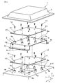
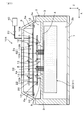
- FIG. 1 is a cross-sectional view illustrating a schematic structure of the power conversion device according to the first embodiment.
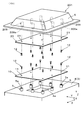
- FIG. 2 is a perspective view showing a fixing structure of each of the first electronic circuit board and the second electronic circuit board in the power conversion device in FIG.
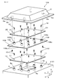
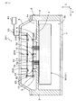
- FIG. 3 is a cross-sectional view illustrating a schematic structure of the power conversion device according to the second embodiment.
- FIG. 4 is a perspective view showing a fixing structure of each of the first electronic circuit board and the second electronic circuit board in the power conversion device in FIG.
- FIG. 5 is a cross-sectional view illustrating a schematic structure of the power conversion device according to the third embodiment.
- FIG. 6 is a perspective view showing a fixing structure of each of the first electronic circuit board and the second electronic circuit board in the power conversion device in FIG.
- the first direction that is the longitudinal direction of the semiconductor module is indicated by an arrow X
- the second direction that is the width direction of the semiconductor module is indicated by an arrow Y
- the first direction and A third direction orthogonal to both of the second directions is indicated by an arrow Z.
- the power conversion device 1 of Embodiment 1 includes a plurality of elements including a first electronic circuit board 10, a second electronic circuit board 20, and a semiconductor module 30. These plural elements are accommodated in an internal space partitioned by the container 2.
- the power conversion device 1 is mounted on, for example, an electric vehicle, a hybrid vehicle, or the like, and is used as an inverter that converts DC power supply power into AC power necessary for driving a drive motor.
- the container 2 includes a case 3, a cover 6 that closes the opening 3 a of the case 3, and a cover 7 that closes the opening 3 b of the case 3.
- the case 3 includes a partition wall 4 that partitions the internal space in the third direction Z.
- the partition wall 4 is provided with a plurality of boss portions (first fixing portions) 5 extending toward the first electronic circuit board 10 in order to fix the first electronic circuit board 10.
- the boss portion 5 is provided with a female screw portion 5a to which a male screw shaft of the screw 12 can be screwed.
- Both the case 3 and the covers 6 and 7 are made of an aluminum-based material mainly composed of aluminum.
- the semiconductor module 30 includes a semiconductor element 31 such as an IGBT that converts DC power to AC power.
- the semiconductor module 30 includes a plurality of control terminals 32 and power terminals (not shown).
- the first electronic circuit board 10 is a high-voltage electronic circuit board (also referred to as a “control circuit board”) having a rectangular shape in plan view and having a drive circuit for driving the semiconductor module 30 to be switched.
- the first electronic circuit board 10 is disposed closer to the semiconductor module 30 than the second electronic circuit board 20 in the third direction Z, which is the thickness direction of the board, and is electrically connected to the plurality of control terminals 32.
- the plurality of control terminals 32 extend from the semiconductor module 30 to the first electronic circuit board 10 through the openings 4 a provided in the partition wall 4 of the case 3. Accordingly, the first electronic circuit board 10 is electrically connected to the semiconductor module 30.
- the second electronic circuit board 20 is a low-voltage electronic circuit board having a rectangular shape having the same dimensions as the first electronic circuit board 10 in plan view and having a control circuit that controls the semiconductor module 30 based on vehicle information. is there.
- the second electronic circuit board 20 is electrically connected to the first electronic circuit board 10 by a conductive member 22 such as a terminal, and is electrically connected to a control unit (ECU) 40 on the vehicle side by a conductive member 23 such as a terminal. It is connected. Accordingly, the second electronic circuit board 20 is electrically connected to the semiconductor module 30.
- An input signal from the control unit 40 is transmitted to the semiconductor module 30 via the first electronic circuit board 10, the conductive member 22, and the second electronic circuit board 20.
- a detection signal such as a current output from the semiconductor module 30 is transmitted to the control unit 40 via the second electronic circuit board 20, the conductive member 22, and the first electronic circuit board 10.
- the first electronic circuit board 10 and the second electronic circuit board 20 are stacked in the third direction Z with a space 2a therebetween. Such an arrangement is effective in reducing the dimension in the direction along the substrate surface as compared with the case of using one electronic circuit board having the functions of these two electronic circuit boards 10 and 20.
- the inter-substrate plate 8 is a plate-like member including a flat plate portion 8a having a rectangular plan view and flange portions 8b provided on both sides in the first direction X of the flat plate portion 8a. Is fixed to the partition wall 4 of the case 3. In a state where the inter-substrate plate 8 is fixed to the partition wall 4, the inter-substrate plate 8 becomes a component of the container 2. In this case, it can be said that the container 2 has the inter-substrate plate 8.
- a plurality of fixing pins (second fixing portions) 9 for fixing the second electronic circuit board 20 are attached to the inter-substrate plate 8.
- the fixing pin 9 is attached to the inter-substrate plate 8 by being press-fitted into a through hole (not shown) provided in the flat plate portion 8 a of the inter-substrate plate 8.
- the fixing pin 9 includes a female screw portion 9a to which a male screw shaft of the screw 12 can be screwed.
- the inter-substrate plate 8 includes a plurality (two in FIG. 2) of insertion holes 8c formed through each flange portion 8b.
- the partition wall 4 includes a female screw portion 4b to which a male screw shaft of the screw 12 can be screwed.
- the inter-substrate plate 8 is configured to be fixed to the partition wall 4 by screwing the male screw shaft of the screw 12 inserted into each insertion hole 8 c into the female screw portion 4 b of the partition wall 4.
- a configuration is adopted in which a female screw portion such as a female screw portion 4b is provided on a boss portion extending from the partition wall 4 toward the inter-substrate plate 8, and the inter-substrate plate 8 is fixed to the boss portion. You can also
- the boss portion 5 is a constituent element of the container 2, and a plurality (eight in FIG. 2) are provided in the partition wall 4 so as to surround the opening 4a.
- a plurality of fixing pins 9 are provided on the flat plate portion 8a of the inter-substrate plate 8 almost without deviation.
- the fixing pin 9 is a constituent element of the container 2 in a state of being attached to the inter-substrate plate 8. Note that the arrangement and number of the boss portions 5 and the fixing pins 9 are not limited to those shown in FIG. 2 and can be variously changed as necessary.
- the first electronic circuit board 10 includes a plurality (eight in FIG. 2) of insertion holes 11 that are formed so as to penetrate in the third direction Z.
- the male screw shaft of the screw 12 inserted into each insertion hole 11 is connected to the female screw part 5 a of the boss part 5 in a state where each insertion hole 11 is aligned with the female screw part 5 a of the boss part 5. It is fixed to the boss portion 5 by screwing. As a result, the first electronic circuit board 10 is fixed to the case 3 of the container 2 while being supported by the plurality of boss portions 5.
- the second electronic circuit board 20 is not interposed between the boss portion 5 (component of the container 2) and the first electronic circuit board 10 in the third direction Z that is the board thickness direction. It is configured as follows. In other words, the boss portion 5 is located at a position where the second electronic circuit board 20 is not interposed between the boss part 5 and the first electronic circuit board 10 in the third direction Z (hereinafter also referred to as “first non-intervening position”). Is provided. This first non-intervening position can also be said to be a position where the fixing with the first electronic circuit board 10 is not disturbed by the second electronic circuit board 20.
- the second electronic circuit board 20 includes a plurality (eight in FIG. 2) of insertion holes 21 that are formed so as to penetrate in the third direction Z.
- the male screw shaft of the screw 12 inserted into each insertion hole 21 is connected to the female screw part 9 a of the fixing pin 9 with each insertion hole 21 aligned with the female screw part 9 a of the fixing pin 9.
- the fixing pin 9 is fixed by screwing.
- the second electronic circuit board 20 is fixed to the case 3 constituting the container 2 while being supported by the plurality of fixing pins 9 of the inter-substrate plate 8.
- the inter-substrate plate 8 fixed to the case 3 is provided with the fixing pin 9 (second fixing portion) for fixing the second electronic circuit board 20, and the container 2 Among them, a boss for fixing the first electronic circuit board 10 to a portion (partition wall 4 of the case 3) opposite to the second electronic circuit board 20 fixed to the inter-board plate 8 with the inter-board plate 8 interposed therebetween.
- a portion 5 (first fixing portion) is provided.
- a configuration in which the first electronic circuit board 10 is fixed to the fixing pin 9 and the second electronic circuit board 20 is fixed to the boss portion 5 may be employed.
- the first electronic circuit board 10 is not obstructed by the second electronic circuit board 20 by providing the boss portion 5 at the first non-intervening position.
- the case 3 can be fixed.
- the second electronic circuit board 20 can be fixed to the case 3 of the container 2 without being obstructed by the first electronic circuit board 10. it can.
- each of the first electronic circuit board 10 and the second electronic circuit board 20 is fixed to the container 2, the arrangement and the number of the fixing portions are not easily limited. Therefore, the number of fixing points of each electronic circuit board can be increased, and the fixing points can be prevented from being biased to, for example, only the four corners of each electronic circuit board. As a result, each electronic circuit board is not easily deformed by an external force, and a desired fixing strength that can withstand vibration received from the vehicle side when the vehicle travels can be secured.
- the boss part 5 cannot be provided in the part of the opening 4a in the partition wall 4. Accordingly, the surface of the first electronic circuit board 10 facing the opening 4a is not supported by the boss portion 5, but is instead supported by a plurality of control terminals 32 arranged in the opening 4a. Thereby, the fall of the fixed strength of the 1st electronic circuit board 10 is controlled.
- the arrangement of the fixing pin 9 in the flat plate portion 8a of the inter-substrate plate 8 is not limited (for example, the fixing pin 9 can be arranged in the central portion of the flat plate portion 8a). The fixing strength of the substrate 20 can be increased.
- the linear expansion coefficient of the inter-substrate plate 8 interposed between the case 3 and the first electronic circuit board 10 is an intermediate value between the linear expansion coefficient of the case 3 and the linear expansion coefficient of the first electronic circuit board 10. Therefore, the influence of thermal strain between these components can be reduced.
- the power conversion device 101 of the second embodiment is different from the power conversion device 1 of the first embodiment in the fixing structure of the second electronic circuit board 20.
- Other configurations are the same as those of the first embodiment. Therefore, only elements related to the fixing structure of the second electronic circuit board 20 will be described with reference to FIGS. 3 and 4 and description of other elements will be omitted. In these drawings, the same elements as those shown in FIGS. 1 and 2 are denoted by the same reference numerals.
- an inter-substrate plate 108 is interposed between the first electronic circuit board 10 and the second electronic circuit board 20 as an interposing member.
- the inter-substrate plate 108 is a plate-like member configured to have a rectangular shape in plan view and to have a size in plan view that exceeds both the first electronic circuit board 10 and the second electronic circuit board 20.
- the cover 6 includes a plurality of boss portions 6 a that extend toward the inter-substrate plate 108.
- the inter-substrate plate 108 is a flat member and is fixed to the boss 6 a of the cover 6 using screws 12.
- the inter-substrate plate 108 In the state where the inter-substrate plate 108 is fixed to the boss 6 a of the cover 6, the inter-substrate plate 108 becomes a constituent element of the container 2. In this case, it can be said that the container 2 has the inter-substrate plate 108.
- the inter-substrate plate 108 is made of the same iron-based material as the inter-substrate plate 8 described above.
- a plurality of fixing pins (second fixing portions) 109 for fixing the second electronic circuit board 20 are attached to the inter-substrate plate 108.
- the fixing pin 109 is attached to the inter-substrate plate 108 by being press-fitted into a through hole (not shown) provided in the inter-substrate plate 108.
- a plurality of fixing pins 109 are provided on the inter-substrate plate 108 with almost no bias.
- the fixing pin 109 includes a female screw portion 109a similar to the female screw portion 9a of the fixing pin 9 described above.
- the fixing pin 109 is a constituent element of the container 2 when attached to the inter-substrate plate 108.
- the arrangement and the number of the fixing pins 109 are not limited to those shown in FIG. 4 and can be variously changed as necessary.
- the male screw shaft of the screw 12 inserted into each insertion hole 21 is screwed into the female screw part 109 a of the fixing pin 109 in a state in which each insertion hole 21 is aligned with the female screw part 109 a of the fixing pin 109.
- the fixing pins 109 are fixed.
- the second electronic circuit board 20 is fixed to the cover 6 constituting the container 2 while being supported by the plurality of fixing pins 109 of the inter-substrate plate 108.
- the first electronic circuit board 10 is not interposed between the fixing pin 109 (component of the container 2) and the second electronic circuit board 20 in the third direction Z. That is, as in the case of the fixing pin 9 described above, the fixing pin 109 is located at a position where the first electronic circuit board 10 is not interposed between the cover 6 and the second electronic circuit board 20 in the third direction Z (second Non-intervening position).
- the inter-substrate plate 108 fixed to the cover 6 is provided with the fixing pin 109 (second fixing portion) for fixing the second electronic circuit board 20, and the container 2.
- a portion 5 (first fixing portion) is provided.
- a configuration in which the first electronic circuit board 10 is fixed to the fixing pins 109 and the second electronic circuit board 20 is fixed to the boss portion 5 may be employed.
- the arrangement of the fixing pins 109 in the inter-substrate plate 108 is not limited (for example, the fixing pins 109 can be arranged in the center of the inter-substrate plate 108), so that the fixing strength of the second electronic circuit board 20 by the fixing pins 109 is increased. Can be high.
- the same effects as those of the first embodiment are obtained.
- the power conversion device 201 of the third embodiment is different from the power conversion device 1 of the first embodiment in the fixing structure of the second electronic circuit board 20.
- Other configurations are the same as those of the first embodiment. Therefore, here, only the fixing structure of the second electronic circuit board 20 will be described with reference to FIGS. 5 and 6, and the other description will be omitted.
- the same elements as those shown in FIGS. 1 and 2 are denoted by the same reference numerals.
- a member such as the inter-substrate plate 8 is not interposed between the first electronic circuit board 10 and the second electronic circuit board 20.
- the cover 6 includes a plurality of boss portions 209 extending on the top plate surface toward the second electronic circuit board 20.
- the male screw shaft of the screw 12 inserted into each insertion hole 21 is screwed into the female screw part 209 a of the boss part 209 with each insertion hole 21 aligned with the female thread part 209 a of the boss part 209.
- the boss portion 209 is fixed.
- the second electronic circuit board 20 is fixed to the cover 6 constituting the container 2.
- the first electronic circuit board 10 is not interposed between the boss portion 209 (component of the container 2) and the second electronic circuit board 20 in the third direction Z.
- the boss portion 209 is located at a position where the first electronic circuit board 10 is not interposed between the cover 6 and the second electronic circuit board 20 in the third direction Z (second second). Non-intervening position).
- the case 3 is provided with the boss portion 5 (first fixing portion) for fixing the first electronic circuit board 10, and the second electronic circuit board 20 is fixed to the cover 6.
- a boss portion 209 (second fixing portion) is provided.
- a configuration in which the second electronic circuit board 20 is fixed to the boss portion 5 and the first electronic circuit board 10 is fixed to the boss portion 209 may be employed.
- the second electronic circuit board 20 can be fixed to the cover 6 of the container 2 without being obstructed by the first electronic circuit board 10. For this reason, when each of the 1st electronic circuit board 10 and the 2nd electronic circuit board 20 is fixed to the container 2, the arrangement
- the arrangement of the boss portion 209 on the top plate surface of the cover 6 is not limited (for example, the boss portion 209 can also be arranged at the center of the top plate surface of the cover 6).
- the fixing strength can be increased.
- the same effects as those of the first embodiment are obtained.
- the case 3 and the cover 6 made of an aluminum-based material and the inter-substrate plates 8 and 108 made of an iron-based material have been exemplified. It can be changed.
- the material is selected such that the inter-substrate plates 8 and 108 are made of a material having a smaller linear expansion coefficient than the case 3 and the cover 6 and having magnetic shielding properties. If necessary, the material of the inter-substrate plates 8 and 108 can be selected without considering the linear expansion coefficient and the magnetic shielding properties.
- the inter-substrate plates 8 and 108 may be made of an aluminum-based material or a resin material.
- inter-substrate plates 8 and 108 which are plate-like members, are interposed between the two electronic circuit boards 10 and 20, but the inter-substrate plates 8 and 108 are used instead.
- a member having a shape other than a plate shape can also be used.
Abstract
A power conversion device (1) is provided with: a semiconductor module (30); a first electronic circuit substrate (10) and a second electronic circuit substrate (20); and an accommodation body (2) for accommodating both the first electronic circuit substrate (10) and the second electronic circuit substrate (20). The accommodation body (2) comprises a first fixing section (5) to which the first electronic circuit substrate (10) is fixed and a second fixing section (9) to which the second electronic circuit substrate (20) is fixed. The accommodation body (2) is configured so that the second electronic circuit substrate (20) is not between the first fixing section (5) of the accommodation body (2) and the first electronic circuit substrate (10) in the substrate thickness direction (Z) and the first electronic circuit substrate (10) is not between the second fixing section (9) of the accommodation body (2) and the second electronic circuit substrate (20) in the substrate thickness direction (Z).
Description
本出願は、2016年2月5日に出願された日本出願番号2016-021061号に基づくもので、ここにその記載内容を援用する。
This application is based on Japanese Application No. 2016-021061 filed on Feb. 5, 2016, the contents of which are incorporated herein by reference.
本開示は、複数の電子回路基板を備えた電力変換装置に関する。
The present disclosure relates to a power conversion device including a plurality of electronic circuit boards.
電気自動車、ハイブリッド自動車等の車両は、直流電力と交流電力との間で電力変換を行う電力変換装置を搭載している。例えば、下記の特許文献1には、半導体素子を内蔵した半導体モジュールと、複数の電子回路基板と、を備えた電力変換装置が開示されている。複数の電子回路基板には、高圧系用の第1電子回路基板と、低圧系用の第2電子回路基板と、が含まれている。第1電子回路基板及び第2電子回路基板は、基板厚み方向に空間を隔てて積層配置された状態で半導体モジュールを収容する収容体の固定面に固定されている。このような積層配置は、電子回路基板の板面に沿った方向の寸法を小さく抑えるのに有効である。
Vehicles such as electric vehicles and hybrid vehicles are equipped with a power conversion device that converts power between DC power and AC power. For example, Patent Document 1 below discloses a power conversion device including a semiconductor module incorporating a semiconductor element and a plurality of electronic circuit boards. The plurality of electronic circuit boards includes a first electronic circuit board for a high voltage system and a second electronic circuit board for a low voltage system. The first electronic circuit board and the second electronic circuit board are fixed to a fixing surface of a container that houses the semiconductor module in a state where the first electronic circuit board and the second electronic circuit board are stacked and arranged with a space therebetween in the substrate thickness direction. Such a stacked arrangement is effective to keep the dimension in the direction along the plate surface of the electronic circuit board small.
上記の電力変換装置の場合、第1電子回路基板が収容体の固定面と第2電子回路基板との間に配置される。このため、第2電子回路基板は、収容体との固定の際に、第1電子回路基板が邪魔になってその固定箇所の数を増やすことができない。例えば、第2電子回路基板の固定箇所が該基板の四隅のみに制限される。また、第2電子回路基板の固定箇所が該第2電子回路基板の外周部のみに偏る。そのため、第2電子回路基板は、外力によって変形し易く、車両走行の際に車両側から受ける振動に耐え得る所望の固定強度の確保が難しい。
In the case of the power conversion device described above, the first electronic circuit board is disposed between the fixed surface of the container and the second electronic circuit board. For this reason, when the second electronic circuit board is fixed to the container, the number of the fixing portions cannot be increased because the first electronic circuit board becomes an obstacle. For example, the fixing location of the second electronic circuit board is limited to only the four corners of the board. Moreover, the fixing location of the second electronic circuit board is biased only to the outer peripheral portion of the second electronic circuit board. Therefore, the second electronic circuit board is easily deformed by an external force, and it is difficult to ensure a desired fixing strength that can withstand vibrations received from the vehicle side during vehicle travel.
本開示は、半導体モジュールに電気的に接続された複数の電子回路基板の固定強度を高めることができる電力変換装置を提供しようとするものである。
This disclosure intends to provide a power conversion device capable of increasing the fixing strength of a plurality of electronic circuit boards electrically connected to a semiconductor module.
本開示の一態様は、
半導体素子を内蔵した半導体モジュールと、
いずれも上記半導体モジュールと電気的に接続され、基板厚み方向に空間を隔てて積層配置された第1電子回路基板及び第2電子回路基板と、
上記半導体モジュール、上記第1電子回路基板及び上記第2電子回路基板を共に収容する収容体と、
を備え、
上記収容体は、上記第1電子回路基板が固定される第1固定部と、上記第2電子回路基板が固定される第2固定部と、を有し、
上記基板厚み方向について上記収容体の上記第1固定部と上記第1電子回路基板との間に上記第2電子回路基板が介在しないように、且つ上記基板厚み方向について上記収容体の上記第2固定部と上記第2電子回路基板との間に上記第1電子回路基板が介在しないように構成されている、電力変換装置にある。 One aspect of the present disclosure is:
A semiconductor module containing a semiconductor element;
A first electronic circuit board and a second electronic circuit board that are both electrically connected to the semiconductor module and arranged in a stacked manner with a space in the substrate thickness direction,
A housing for housing both the semiconductor module, the first electronic circuit board, and the second electronic circuit board;
With
The container includes a first fixing portion to which the first electronic circuit board is fixed, and a second fixing portion to which the second electronic circuit board is fixed.
The second electronic circuit board is not interposed between the first fixing part of the container and the first electronic circuit board in the substrate thickness direction, and the second of the container in the substrate thickness direction. The power converter is configured such that the first electronic circuit board is not interposed between the fixing portion and the second electronic circuit board.
上記電力変換装置によれば、第1電子回路基板を第2電子回路基板に邪魔されることなく収容体に固定することができる。同様に、第2電子回路基板を第1電子回路基板に邪魔されることなく収容体に固定することができる。このため、第1電子回路基板及び第2電子回路基板のそれぞれを収容体に固定する際に、その固定箇所の配置及び数が制限されにくい。従って、各電子回路基板の固定箇所を増やすことができ、またその固定箇所が各電子回路基板の例えば四隅のみに偏るのを防止できる。その結果、各電子回路基板が外力によって変形しにくく、各電子回路基板について車両走行の際に車両側から受ける振動に耐え得る所望の固定強度を確保することができる。
According to the power conversion device, the first electronic circuit board can be fixed to the container without being obstructed by the second electronic circuit board. Similarly, the second electronic circuit board can be fixed to the container without being obstructed by the first electronic circuit board. For this reason, when each of a 1st electronic circuit board and a 2nd electronic circuit board is fixed to a container, arrangement | positioning and the number of the fixing location are not easily restricted. Therefore, the number of fixing points of each electronic circuit board can be increased, and the fixing points can be prevented from being biased to, for example, only the four corners of each electronic circuit board. As a result, each electronic circuit board is not easily deformed by an external force, and a desired fixing strength that can withstand vibration received from the vehicle side when the vehicle travels can be secured.
以上のごとく、上記態様によれば、半導体モジュールに電気的に接続された複数の電子回路基板の固定強度を高めることができる。
As described above, according to the above aspect, the fixing strength of a plurality of electronic circuit boards electrically connected to the semiconductor module can be increased.
本開示についての上記目的およびその他の目的、特徴や利点は、添付の図面を参照しながら下記の詳細な記述により、より明確になる。その図面は、
図1は、実施形態1の電力変換装置の概略構造を示す断面図であり、
図2は、図1中の電力変換装置における第1電子回路基板及び第2電子回路基板のそれぞれの固定構造を示す斜視図であり、
図3は、実施形態2の電力変換装置の概略構造を示す断面図であり、
図4は、図3中の電力変換装置における第1電子回路基板及び第2電子回路基板のそれぞれの固定構造を示す斜視図であり、
図5は、実施形態3の電力変換装置の概略構造を示す断面図であり、
図6は、図5中の電力変換装置における第1電子回路基板及び第2電子回路基板のそれぞれの固定構造を示す斜視図である。
The above and other objects, features and advantages of the present disclosure will become more apparent from the following detailed description with reference to the accompanying drawings. The drawing
FIG. 1 is a cross-sectional view illustrating a schematic structure of the power conversion device according to the first embodiment. FIG. 2 is a perspective view showing a fixing structure of each of the first electronic circuit board and the second electronic circuit board in the power conversion device in FIG. FIG. 3 is a cross-sectional view illustrating a schematic structure of the power conversion device according to the second embodiment. FIG. 4 is a perspective view showing a fixing structure of each of the first electronic circuit board and the second electronic circuit board in the power conversion device in FIG. FIG. 5 is a cross-sectional view illustrating a schematic structure of the power conversion device according to the third embodiment. FIG. 6 is a perspective view showing a fixing structure of each of the first electronic circuit board and the second electronic circuit board in the power conversion device in FIG.
以下、電力変換装置に係る実施形態について、図面を参照しつつ説明する。
Hereinafter, embodiments of the power conversion device will be described with reference to the drawings.
なお、本明細書の図面では、特に断わらない限り、半導体モジュールの長手方向である第1方向を矢印Xで示し、半導体モジュールの幅方向である第2方向を矢印Yで示し、第1方向及び第2方向の双方と直交する第3方向を矢印Zで示すものとする。
In the drawings of this specification, unless otherwise specified, the first direction that is the longitudinal direction of the semiconductor module is indicated by an arrow X, the second direction that is the width direction of the semiconductor module is indicated by an arrow Y, and the first direction and A third direction orthogonal to both of the second directions is indicated by an arrow Z.
(実施形態1)
図1に示されるように、実施形態1の電力変換装置1は、第1電子回路基板10、第2電子回路基板20及び半導体モジュール30を含む複数の要素を備えている。これら複数の要素は収容体2によって区画された内部空間に収容されている。この電力変換装置1は、例えば、電気自動車やハイブリッド自動車等に搭載され、直流の電源電力を駆動用モータの駆動に必要な交流電力に変換するインバータとして用いられる。 (Embodiment 1)
As shown in FIG. 1, thepower conversion device 1 of Embodiment 1 includes a plurality of elements including a first electronic circuit board 10, a second electronic circuit board 20, and a semiconductor module 30. These plural elements are accommodated in an internal space partitioned by the container 2. The power conversion device 1 is mounted on, for example, an electric vehicle, a hybrid vehicle, or the like, and is used as an inverter that converts DC power supply power into AC power necessary for driving a drive motor.
図1に示されるように、実施形態1の電力変換装置1は、第1電子回路基板10、第2電子回路基板20及び半導体モジュール30を含む複数の要素を備えている。これら複数の要素は収容体2によって区画された内部空間に収容されている。この電力変換装置1は、例えば、電気自動車やハイブリッド自動車等に搭載され、直流の電源電力を駆動用モータの駆動に必要な交流電力に変換するインバータとして用いられる。 (Embodiment 1)
As shown in FIG. 1, the
収容体2は、ケース3と、ケース3の開口3aを塞ぐカバー6と、ケース3の開口3bを塞ぐカバー7と、を有する。ケース3は、第3方向Zについて内部空間を仕切る仕切壁4を備えている。仕切壁4には、第1電子回路基板10の固定のために該第1電子回路基板10に向けて延出する複数のボス部(第1固定部)5が設けられている。ボス部5には、ビス12の雄ねじ軸が螺合可能な雌ねじ部5aが設けられている。ケース3及びカバー6,7はいずれもアルミニウムを主体としたアルミニウム系材料からなる。
The container 2 includes a case 3, a cover 6 that closes the opening 3 a of the case 3, and a cover 7 that closes the opening 3 b of the case 3. The case 3 includes a partition wall 4 that partitions the internal space in the third direction Z. The partition wall 4 is provided with a plurality of boss portions (first fixing portions) 5 extending toward the first electronic circuit board 10 in order to fix the first electronic circuit board 10. The boss portion 5 is provided with a female screw portion 5a to which a male screw shaft of the screw 12 can be screwed. Both the case 3 and the covers 6 and 7 are made of an aluminum-based material mainly composed of aluminum.
半導体モジュール30は、直流電力を交流電力に変換するIGBT等の半導体素子31を内蔵している。半導体モジュール30は、複数の制御端子32及びパワー端子(図示省略)を備えている。
The semiconductor module 30 includes a semiconductor element 31 such as an IGBT that converts DC power to AC power. The semiconductor module 30 includes a plurality of control terminals 32 and power terminals (not shown).
第1電子回路基板10は、平面視が矩形であり、半導体モジュール30をスイッチング駆動させるための駆動回路を有する高電圧系の電子回路基板(「制御回路基板」ともいう。)である。この目的のために、第1電子回路基板10は、基板厚み方向である第3方向Zについて第2電子回路基板20よりも半導体モジュール30に近い位置に配置され、且つ複数の制御端子32に電気的に接続されている。複数の制御端子32は、ケース3の仕切壁4に設けられた開口4aを通じて半導体モジュール30から第1電子回路基板10まで延在している。従って、第1電子回路基板10は、半導体モジュール30に電気的に接続されている。
The first electronic circuit board 10 is a high-voltage electronic circuit board (also referred to as a “control circuit board”) having a rectangular shape in plan view and having a drive circuit for driving the semiconductor module 30 to be switched. For this purpose, the first electronic circuit board 10 is disposed closer to the semiconductor module 30 than the second electronic circuit board 20 in the third direction Z, which is the thickness direction of the board, and is electrically connected to the plurality of control terminals 32. Connected. The plurality of control terminals 32 extend from the semiconductor module 30 to the first electronic circuit board 10 through the openings 4 a provided in the partition wall 4 of the case 3. Accordingly, the first electronic circuit board 10 is electrically connected to the semiconductor module 30.
第2電子回路基板20は、平面視が第1電子回路基板10と同様の寸法を有する矩形であり、車両情報に基づいて半導体モジュール30を制御する制御回路を有する低電圧系の電子回路基板である。この第2電子回路基板20は、ターミナル等の導電部材22によって第1電子回路基板10に電気的に接続され、且つターミナル等の導電部材23によって車両側の制御部(ECU)40に電気的に接続されている。従って、第2電子回路基板20は、半導体モジュール30に電気的に接続されている。制御部40からの入力信号は、第1電子回路基板10、導電部材22及び第2電子回路基板20を介して半導体モジュール30に伝送される。一方で、半導体モジュール30から出力される電流等の検出信号は、第2電子回路基板20、導電部材22及び第1電子回路基板10を介して制御部40に伝送される。
The second electronic circuit board 20 is a low-voltage electronic circuit board having a rectangular shape having the same dimensions as the first electronic circuit board 10 in plan view and having a control circuit that controls the semiconductor module 30 based on vehicle information. is there. The second electronic circuit board 20 is electrically connected to the first electronic circuit board 10 by a conductive member 22 such as a terminal, and is electrically connected to a control unit (ECU) 40 on the vehicle side by a conductive member 23 such as a terminal. It is connected. Accordingly, the second electronic circuit board 20 is electrically connected to the semiconductor module 30. An input signal from the control unit 40 is transmitted to the semiconductor module 30 via the first electronic circuit board 10, the conductive member 22, and the second electronic circuit board 20. On the other hand, a detection signal such as a current output from the semiconductor module 30 is transmitted to the control unit 40 via the second electronic circuit board 20, the conductive member 22, and the first electronic circuit board 10.
第1電子回路基板10及び第2電子回路基板20は、第3方向Zに空間2aを隔てて積層配置されている。このような配置は、これら2つの電子回路基板10,20の機能を兼ね備えた1つの電子回路基板を用いる場合に比べて、基板面に沿った方向の寸法を小さく抑えるのに有効である。
The first electronic circuit board 10 and the second electronic circuit board 20 are stacked in the third direction Z with a space 2a therebetween. Such an arrangement is effective in reducing the dimension in the direction along the substrate surface as compared with the case of using one electronic circuit board having the functions of these two electronic circuit boards 10 and 20.
第1電子回路基板10と第2電子回路基板20との間には、介装部材としての基板間プレート8が介装されている。この基板間プレート8は、平面視が矩形の平板部8aと、平板部8aの第1方向Xの両側に設けられたフランジ部8bと、を備える板状部材であり、フランジ部8bがビス12を用いてケース3の仕切壁4に固定されている。基板間プレート8が仕切壁4に固定された状態では、この基板間プレート8が収容体2の構成要素となる。この場合、収容体2が基板間プレート8を有するということができる。
Between the first electronic circuit board 10 and the second electronic circuit board 20, an inter-substrate plate 8 is interposed as an interposing member. The inter-substrate plate 8 is a plate-like member including a flat plate portion 8a having a rectangular plan view and flange portions 8b provided on both sides in the first direction X of the flat plate portion 8a. Is fixed to the partition wall 4 of the case 3. In a state where the inter-substrate plate 8 is fixed to the partition wall 4, the inter-substrate plate 8 becomes a component of the container 2. In this case, it can be said that the container 2 has the inter-substrate plate 8.
基板間プレート8は、第3方向Zについて第1電子回路基板10及び第2電子回路基板20の一方から他方を遮蔽する大きさ(以下、「遮蔽寸法」ともいう。)を有する。即ち、この基板間プレート8は、平面視の大きさが第1電子回路基板10及び第2電子回路基板20の双方を上回るように構成されている。また、基板間プレート8は、鉄を主体とした鉄系材料からなる。この鉄系材料は、磁気遮蔽性を有する材料であり、且つケース3及びカバー6を構成するアルミニウム系材料よりも線膨張率(固体の熱膨張による長さの増加の割合を温度差で割った値)の小さい材料である。
The inter-substrate plate 8 has a size that shields one of the first electronic circuit board 10 and the second electronic circuit board 20 from the other in the third direction Z (hereinafter also referred to as “shielding dimension”). That is, the inter-substrate plate 8 is configured such that the size in plan view exceeds both the first electronic circuit board 10 and the second electronic circuit board 20. The inter-substrate plate 8 is made of an iron-based material mainly composed of iron. This iron-based material is a material having magnetic shielding properties, and the linear expansion coefficient (the rate of increase in length due to the thermal expansion of the solid divided by the temperature difference) than the aluminum-based material constituting the case 3 and the cover 6. Value).
基板間プレート8には、第2電子回路基板20の固定のための複数の固定ピン(第2固定部)9が取付けられている。固定ピン9は、基板間プレート8の平板部8aに設けられた貫通孔(図示省略)に圧入されることによって基板間プレート8に取付けられている。この固定ピン9は、ビス12の雄ねじ軸が螺合可能な雌ねじ部9aを備えている。
A plurality of fixing pins (second fixing portions) 9 for fixing the second electronic circuit board 20 are attached to the inter-substrate plate 8. The fixing pin 9 is attached to the inter-substrate plate 8 by being press-fitted into a through hole (not shown) provided in the flat plate portion 8 a of the inter-substrate plate 8. The fixing pin 9 includes a female screw portion 9a to which a male screw shaft of the screw 12 can be screwed.
図2に示されるように、基板間プレート8は、各フランジ部8bに貫通形成された複数(図2では2つ)の挿入孔8cを備えている。仕切壁4は、ビス12の雄ねじ軸が螺合可能な雌ねじ部4bを備えている。基板間プレート8は、各挿入孔8cに挿入されたビス12の雄ねじ軸が仕切壁4の雌ねじ部4bに螺合することによって仕切壁4に固定されるように構成されている。なお、本構成に代えて、仕切壁4から基板間プレート8に向けて延出するボス部に雌ねじ部4bのような雌ねじ部を設け、該ボス部に基板間プレート8を固定する構成を採用することもできる。
As shown in FIG. 2, the inter-substrate plate 8 includes a plurality (two in FIG. 2) of insertion holes 8c formed through each flange portion 8b. The partition wall 4 includes a female screw portion 4b to which a male screw shaft of the screw 12 can be screwed. The inter-substrate plate 8 is configured to be fixed to the partition wall 4 by screwing the male screw shaft of the screw 12 inserted into each insertion hole 8 c into the female screw portion 4 b of the partition wall 4. Instead of this configuration, a configuration is adopted in which a female screw portion such as a female screw portion 4b is provided on a boss portion extending from the partition wall 4 toward the inter-substrate plate 8, and the inter-substrate plate 8 is fixed to the boss portion. You can also
ボス部5は、収容体2の構成要素であり、仕切壁4に開口4aを取り囲むように複数(図2では8つ)設けられている。固定ピン9は、基板間プレート8の平板部8aにほぼ偏りなく複数(図2では9つ)設けられている。この固定ピン9は、基板間プレート8に取付けられた状態で収容体2の構成要素となる。なお、これらボス部5及び固定ピン9のそれぞれの配置及び数は、図2に示すものに限定されるものではなく、必要に応じて種々変更が可能である。
The boss portion 5 is a constituent element of the container 2, and a plurality (eight in FIG. 2) are provided in the partition wall 4 so as to surround the opening 4a. A plurality of fixing pins 9 (nine in FIG. 2) are provided on the flat plate portion 8a of the inter-substrate plate 8 almost without deviation. The fixing pin 9 is a constituent element of the container 2 in a state of being attached to the inter-substrate plate 8. Note that the arrangement and number of the boss portions 5 and the fixing pins 9 are not limited to those shown in FIG. 2 and can be variously changed as necessary.
第1電子回路基板10は、いずれも第3方向Zに貫通形成された複数(図2では8つ)の挿入孔11を備えている。この第1電子回路基板10は、各挿入孔11をボス部5の雌ねじ部5aに位置合わせした状態で、各挿入孔11に挿入されたビス12の雄ねじ軸をボス部5の雌ねじ部5aに螺合させることによってボス部5に固定される。その結果、第1電子回路基板10は、複数のボス部5によって支持された状態で収容体2のケース3に固定される。
The first electronic circuit board 10 includes a plurality (eight in FIG. 2) of insertion holes 11 that are formed so as to penetrate in the third direction Z. In the first electronic circuit board 10, the male screw shaft of the screw 12 inserted into each insertion hole 11 is connected to the female screw part 5 a of the boss part 5 in a state where each insertion hole 11 is aligned with the female screw part 5 a of the boss part 5. It is fixed to the boss portion 5 by screwing. As a result, the first electronic circuit board 10 is fixed to the case 3 of the container 2 while being supported by the plurality of boss portions 5.
この場合、電力変換装置1は、基板厚み方向である第3方向Zについてボス部5(収容体2の構成要素)と第1電子回路基板10との間に第2電子回路基板20が介在しないように構成されている。換言すれば、ボス部5は、第3方向Zについて第1電子回路基板10との間に第2電子回路基板20が介在しない位置(以下、「第1の非介在位置」ともいう。)に設けられている。この第1の非介在位置を、第1電子回路基板10との固定が第2電子回路基板20によって邪魔されない位置ということもできる。
In this case, in the power conversion device 1, the second electronic circuit board 20 is not interposed between the boss portion 5 (component of the container 2) and the first electronic circuit board 10 in the third direction Z that is the board thickness direction. It is configured as follows. In other words, the boss portion 5 is located at a position where the second electronic circuit board 20 is not interposed between the boss part 5 and the first electronic circuit board 10 in the third direction Z (hereinafter also referred to as “first non-intervening position”). Is provided. This first non-intervening position can also be said to be a position where the fixing with the first electronic circuit board 10 is not disturbed by the second electronic circuit board 20.
第2電子回路基板20は、いずれも第3方向Zに貫通形成された複数(図2では8つ)の挿入孔21を備えている。この第2電子回路基板20は、各挿入孔21を固定ピン9の雌ねじ部9aに位置合わせした状態で、各挿入孔21に挿入されたビス12の雄ねじ軸を固定ピン9の雌ねじ部9aに螺合させることによって固定ピン9に固定される。その結果、第2電子回路基板20は、基板間プレート8の複数の固定ピン9によって支持された状態で、収容体2を構成するケース3に固定される。
The second electronic circuit board 20 includes a plurality (eight in FIG. 2) of insertion holes 21 that are formed so as to penetrate in the third direction Z. In the second electronic circuit board 20, the male screw shaft of the screw 12 inserted into each insertion hole 21 is connected to the female screw part 9 a of the fixing pin 9 with each insertion hole 21 aligned with the female screw part 9 a of the fixing pin 9. The fixing pin 9 is fixed by screwing. As a result, the second electronic circuit board 20 is fixed to the case 3 constituting the container 2 while being supported by the plurality of fixing pins 9 of the inter-substrate plate 8.
この場合、電力変換装置1は、基板厚み方向である第3方向Zについて固定ピン9(収容体2の構成要素)と第2電子回路基板20との間に第1電子回路基板10が介在しないように構成されている。換言すれば、固定ピン9は、ケース3のうち第3方向Zについて第2電子回路基板20との間に第1電子回路基板10が介在しない位置(以下、「第2の非介在位置」ともいう。)に設けられている。この第2の非介在位置を、第2電子回路基板20との固定が第1電子回路基板10によって邪魔されない位置ということもできる。
In this case, in the power conversion device 1, the first electronic circuit board 10 is not interposed between the fixing pin 9 (component of the container 2) and the second electronic circuit board 20 in the third direction Z that is the board thickness direction. It is configured as follows. In other words, the fixing pin 9 is a position where the first electronic circuit board 10 is not interposed between the case 3 and the second electronic circuit board 20 in the third direction Z (hereinafter referred to as “second non-intervening position”). ). This second non-intervening position can also be said to be a position where the fixing with the second electronic circuit board 20 is not disturbed by the first electronic circuit board 10.
このように、実施形態1の場合、ケース3に固定された基板間プレート8に第2電子回路基板20の固定のための固定ピン9(第2固定部)が設けられ、且つ収容体2のうち基板間プレート8を挟んで該基板間プレート8に固定される第2電子回路基板20とは反対側の部位(ケース3の仕切壁4)に第1電子回路基板10の固定のためのボス部5(第1固定部)が設けられるように構成されている。なお、本構成に代えて、第1電子回路基板10が固定ピン9に固定され、且つ第2電子回路基板20がボス部5に固定される構成を採用することもできる。
As described above, in the first embodiment, the inter-substrate plate 8 fixed to the case 3 is provided with the fixing pin 9 (second fixing portion) for fixing the second electronic circuit board 20, and the container 2 Among them, a boss for fixing the first electronic circuit board 10 to a portion (partition wall 4 of the case 3) opposite to the second electronic circuit board 20 fixed to the inter-board plate 8 with the inter-board plate 8 interposed therebetween. A portion 5 (first fixing portion) is provided. Instead of this configuration, a configuration in which the first electronic circuit board 10 is fixed to the fixing pin 9 and the second electronic circuit board 20 is fixed to the boss portion 5 may be employed.
次に、実施形態1の電力変換装置1の作用効果について説明する。
Next, functions and effects of the power conversion device 1 according to the first embodiment will be described.
上記の電力変換装置1によれば、ボス部5を上記の第1の非介在位置に設けることによって、第1電子回路基板10を第2電子回路基板20によって邪魔されることなく収容体2のケース3に固定することができる。同様に、固定ピン9を上記の第2の非介在位置に設けることによって、第2電子回路基板20を第1電子回路基板10によって邪魔されることなく収容体2のケース3に固定することができる。
According to the power conversion device 1 described above, the first electronic circuit board 10 is not obstructed by the second electronic circuit board 20 by providing the boss portion 5 at the first non-intervening position. The case 3 can be fixed. Similarly, by providing the fixing pin 9 at the second non-intervening position, the second electronic circuit board 20 can be fixed to the case 3 of the container 2 without being obstructed by the first electronic circuit board 10. it can.
このため、第1電子回路基板10及び第2電子回路基板20のそれぞれを収容体2に固定する際に、その固定箇所の配置及び数が制限されにくい。従って、各電子回路基板の固定箇所を増やすことができ、またその固定箇所が各電子回路基板の例えば四隅のみに偏るのを防止できる。その結果、各電子回路基板が外力によって変形しにくく、各電子回路基板について車両走行の際に車両側から受ける振動に耐え得る所望の固定強度を確保することができる。
For this reason, when each of the first electronic circuit board 10 and the second electronic circuit board 20 is fixed to the container 2, the arrangement and the number of the fixing portions are not easily limited. Therefore, the number of fixing points of each electronic circuit board can be increased, and the fixing points can be prevented from being biased to, for example, only the four corners of each electronic circuit board. As a result, each electronic circuit board is not easily deformed by an external force, and a desired fixing strength that can withstand vibration received from the vehicle side when the vehicle travels can be secured.
なお、仕切壁4のうち開口4aの部位にボス部5を設けることができない。従って、第1電子回路基板10の開口4aとの対向面は、ボス部5によって支持されないが、その代わりに開口4aに配置される複数の制御端子32によって支持されている。これにより、第1電子回路基板10の固定強度の低下が抑えられている。これに対して、基板間プレート8の平板部8aにおける固定ピン9の配置は制限されない(例えば、平板部8aの中央部にも固定ピン9を配置できる)ため、固定ピン9による第2電子回路基板20の固定強度を高くできる。
In addition, the boss part 5 cannot be provided in the part of the opening 4a in the partition wall 4. Accordingly, the surface of the first electronic circuit board 10 facing the opening 4a is not supported by the boss portion 5, but is instead supported by a plurality of control terminals 32 arranged in the opening 4a. Thereby, the fall of the fixed strength of the 1st electronic circuit board 10 is controlled. On the other hand, the arrangement of the fixing pin 9 in the flat plate portion 8a of the inter-substrate plate 8 is not limited (for example, the fixing pin 9 can be arranged in the central portion of the flat plate portion 8a). The fixing strength of the substrate 20 can be increased.
また、上記の電力変換装置1によれば、第1電子回路基板10と第2電子回路基板20との間の基板間プレート8は、上記遮蔽寸法を有し且つ磁気遮蔽性を有する材料からなるため、所謂「シールド板」としての機能を有する。このため、特に、高電圧系の第1電子回路基板10で発生したノイズの影響が低電圧系の第2電子回路基板20に及ぶのを抑制できる。
Moreover, according to said power converter device 1, the board | substrate board 8 between the 1st electronic circuit board 10 and the 2nd electronic circuit board 20 consists of a material which has the said shielding dimension and has magnetic shielding. Therefore, it functions as a so-called “shield plate”. For this reason, in particular, it is possible to suppress the influence of noise generated in the high-voltage first electronic circuit board 10 from reaching the low-voltage second electronic circuit board 20.
また、上記の電力変換装置1によれば、基板間プレート8は、該基板間プレート8が固定されるケース3よりも線膨張率の小さい材料からなる。このため、ケース3が半導体モジュール30などの発熱部品から受ける熱によって歪んだ場合でも、基板間プレート8がケース3によって引っ張られて歪むのを抑制できる。
さらに、基板間プレート8の線膨張率は、ケース3より小さく且つ第1電子回路基板10よりも大きい値であるのが好ましい。これにより、熱膨張率の大きさが、大きい方から順番にケース3、基板間プレート8、第1電子回路基板10となる。この場合、ケース3と第1電子回路基板10との間に介在する基板間プレート8の線膨張率は、ケース3の線膨張率と第1電子回路基板10の線膨張率との中間の値となるため、これら部品間の熱歪の影響を小さくすることができる。 Moreover, according to saidpower converter device 1, the board | substrate plate 8 consists of material with a smaller linear expansion coefficient than the case 3 to which this board | substrate plate 8 is fixed. For this reason, even when the case 3 is distorted by heat received from a heat-generating component such as the semiconductor module 30, it is possible to suppress the inter-substrate plate 8 from being pulled and distorted by the case 3.
Further, the linear expansion coefficient of theinter-substrate plate 8 is preferably smaller than the case 3 and larger than the first electronic circuit board 10. Thereby, the case 3, the board | substrate board 8, and the 1st electronic circuit board 10 are set to the magnitude | size of a coefficient of thermal expansion in an order from the largest. In this case, the linear expansion coefficient of the inter-substrate plate 8 interposed between the case 3 and the first electronic circuit board 10 is an intermediate value between the linear expansion coefficient of the case 3 and the linear expansion coefficient of the first electronic circuit board 10. Therefore, the influence of thermal strain between these components can be reduced.
さらに、基板間プレート8の線膨張率は、ケース3より小さく且つ第1電子回路基板10よりも大きい値であるのが好ましい。これにより、熱膨張率の大きさが、大きい方から順番にケース3、基板間プレート8、第1電子回路基板10となる。この場合、ケース3と第1電子回路基板10との間に介在する基板間プレート8の線膨張率は、ケース3の線膨張率と第1電子回路基板10の線膨張率との中間の値となるため、これら部品間の熱歪の影響を小さくすることができる。 Moreover, according to said
Further, the linear expansion coefficient of the
(実施形態2)
実施形態2の電力変換装置101は、実施形態1の電力変換装置1とは第2電子回路基板20の固定構造が異なる。その他の構成は、実施形態1と同様である。従って、ここでは図3及び図4を参照しつつ第2電子回路基板20の固定構造に関連する要素のみについて説明するものとし、その他の要素の説明は省略する。また、これらの図面において、図1及び図2に示される要素と同一の要素には同一の符号を付している。 (Embodiment 2)
Thepower conversion device 101 of the second embodiment is different from the power conversion device 1 of the first embodiment in the fixing structure of the second electronic circuit board 20. Other configurations are the same as those of the first embodiment. Therefore, only elements related to the fixing structure of the second electronic circuit board 20 will be described with reference to FIGS. 3 and 4 and description of other elements will be omitted. In these drawings, the same elements as those shown in FIGS. 1 and 2 are denoted by the same reference numerals.
実施形態2の電力変換装置101は、実施形態1の電力変換装置1とは第2電子回路基板20の固定構造が異なる。その他の構成は、実施形態1と同様である。従って、ここでは図3及び図4を参照しつつ第2電子回路基板20の固定構造に関連する要素のみについて説明するものとし、その他の要素の説明は省略する。また、これらの図面において、図1及び図2に示される要素と同一の要素には同一の符号を付している。 (Embodiment 2)
The
図3に示されるように、第1電子回路基板10と第2電子回路基板20との間には、介装部材としての基板間プレート108が介装されている。この基板間プレート108は、平面視が矩形であり、平面視の大きさが第1電子回路基板10及び第2電子回路基板20の双方を上回るように構成された板状部材である。また、カバー6は、いずれも基板間プレート108に向けて延出する複数のボス部6aを備えている。基板間プレート108は、平板状の部材であり、ビス12を用いてカバー6のボス部6aに固定されている。基板間プレート108がカバー6のボス部6aに固定された状態では、この基板間プレート108が収容体2の構成要素となる。この場合、収容体2が基板間プレート108を有するということができる。この基板間プレート108は、上記の基板間プレート8と同様の鉄系材料からなる。
As shown in FIG. 3, an inter-substrate plate 108 is interposed between the first electronic circuit board 10 and the second electronic circuit board 20 as an interposing member. The inter-substrate plate 108 is a plate-like member configured to have a rectangular shape in plan view and to have a size in plan view that exceeds both the first electronic circuit board 10 and the second electronic circuit board 20. Further, the cover 6 includes a plurality of boss portions 6 a that extend toward the inter-substrate plate 108. The inter-substrate plate 108 is a flat member and is fixed to the boss 6 a of the cover 6 using screws 12. In the state where the inter-substrate plate 108 is fixed to the boss 6 a of the cover 6, the inter-substrate plate 108 becomes a constituent element of the container 2. In this case, it can be said that the container 2 has the inter-substrate plate 108. The inter-substrate plate 108 is made of the same iron-based material as the inter-substrate plate 8 described above.
基板間プレート108には、第2電子回路基板20の固定のための複数の固定ピン(第2固定部)109が取付けられている。固定ピン109は、基板間プレート108に設けられた貫通孔(図示省略)に圧入されることによって基板間プレート108に取付けられている。
A plurality of fixing pins (second fixing portions) 109 for fixing the second electronic circuit board 20 are attached to the inter-substrate plate 108. The fixing pin 109 is attached to the inter-substrate plate 108 by being press-fitted into a through hole (not shown) provided in the inter-substrate plate 108.
図4に示されるように、基板間プレート108は、複数(図4では2つ)の挿入孔108aを備えている。一方で、カバー6のボス部6aは、ビス12の雄ねじ軸が螺合可能な雌ねじ部6bを備えている。従って、基板間プレート108は、各挿入孔108aに挿入されたビス12の雄ねじ軸がボス部6aの雌ねじ部6bに螺合することによってボス部6aに固定される。
As shown in FIG. 4, the inter-substrate plate 108 has a plurality (two in FIG. 4) of insertion holes 108a. On the other hand, the boss portion 6a of the cover 6 includes a female screw portion 6b to which the male screw shaft of the screw 12 can be screwed. Therefore, the inter-substrate plate 108 is fixed to the boss portion 6a when the male screw shaft of the screw 12 inserted into each insertion hole 108a is screwed into the female screw portion 6b of the boss portion 6a.
固定ピン109は、基板間プレート108にほぼ偏りなく複数(図4では9つ)設けられている。この固定ピン109は、上記の固定ピン9の雌ねじ部9aと同様の雌ねじ部109aを備えている。この固定ピン109は、基板間プレート108に取付けられた状態で収容体2の構成要素となる。なお、この固定ピン109の配置及び数は、図4に示すものに限定されるものではなく、必要に応じて種々変更が可能である。
A plurality of fixing pins 109 (nine in FIG. 4) are provided on the inter-substrate plate 108 with almost no bias. The fixing pin 109 includes a female screw portion 109a similar to the female screw portion 9a of the fixing pin 9 described above. The fixing pin 109 is a constituent element of the container 2 when attached to the inter-substrate plate 108. The arrangement and the number of the fixing pins 109 are not limited to those shown in FIG. 4 and can be variously changed as necessary.
第2電子回路基板20は、各挿入孔21を固定ピン109の雌ねじ部109aに位置合わせした状態で、各挿入孔21に挿入されたビス12の雄ねじ軸を固定ピン109の雌ねじ部109aに螺合させることによって固定ピン109に固定される。その結果、第2電子回路基板20は、基板間プレート108の複数の固定ピン109によって支持された状態で、収容体2を構成するカバー6に固定される。この場合、第3方向Zについて固定ピン109(収容体2の構成要素)と第2電子回路基板20との間に第1電子回路基板10が介在しない。即ち、固定ピン109は、上記の固定ピン9の場合と同様に、カバー6のうち第3方向Zについて第2電子回路基板20との間に第1電子回路基板10が介在しない位置(第2の非介在位置)に設けられている。
In the second electronic circuit board 20, the male screw shaft of the screw 12 inserted into each insertion hole 21 is screwed into the female screw part 109 a of the fixing pin 109 in a state in which each insertion hole 21 is aligned with the female screw part 109 a of the fixing pin 109. By fixing, the fixing pins 109 are fixed. As a result, the second electronic circuit board 20 is fixed to the cover 6 constituting the container 2 while being supported by the plurality of fixing pins 109 of the inter-substrate plate 108. In this case, the first electronic circuit board 10 is not interposed between the fixing pin 109 (component of the container 2) and the second electronic circuit board 20 in the third direction Z. That is, as in the case of the fixing pin 9 described above, the fixing pin 109 is located at a position where the first electronic circuit board 10 is not interposed between the cover 6 and the second electronic circuit board 20 in the third direction Z (second Non-intervening position).
このように、実施形態2の場合、カバー6に固定された基板間プレート108に第2電子回路基板20の固定のための固定ピン109(第2固定部)が設けられ、且つ収容体2のうち基板間プレート108を挟んで該基板間プレート108に固定される第2電子回路基板20とは反対側の部位(ケース3の仕切壁4)に第1電子回路基板10の固定のためのボス部5(第1固定部)が設けられるように構成されている。なお、本構成に代えて、第1電子回路基板10が固定ピン109に固定され、且つ第2電子回路基板20がボス部5に固定される構成を採用することもできる。
As described above, in the case of the second embodiment, the inter-substrate plate 108 fixed to the cover 6 is provided with the fixing pin 109 (second fixing portion) for fixing the second electronic circuit board 20, and the container 2. Among them, a boss for fixing the first electronic circuit board 10 to a part (partition wall 4 of the case 3) opposite to the second electronic circuit board 20 fixed to the inter-board plate 108 with the inter-board plate 108 interposed therebetween. A portion 5 (first fixing portion) is provided. Instead of this configuration, a configuration in which the first electronic circuit board 10 is fixed to the fixing pins 109 and the second electronic circuit board 20 is fixed to the boss portion 5 may be employed.
実施形態2によれば、実施形態1の場合と同様に、第2電子回路基板20を第1電子回路基板10に邪魔されることなく収容体2のカバー6に固定することができる。このため、第1電子回路基板10及び第2電子回路基板20のそれぞれを収容体2に固定する際に、その固定箇所の配置及び数が制限されにくい。その結果、各電子回路基板が外力によって変形しにくく、各電子回路基板について車両走行の際に車両側から受ける振動に耐え得る所望の固定強度を確保することができる。特に、基板間プレート108における固定ピン109の配置は制限されない(例えば、基板間プレート108の中央部にも固定ピン109を配置できる)ため、固定ピン109による第2電子回路基板20の固定強度を高くできる。
その他、実施形態1と同様の作用効果を奏する。 According to the second embodiment, similarly to the first embodiment, the secondelectronic circuit board 20 can be fixed to the cover 6 of the container 2 without being obstructed by the first electronic circuit board 10. For this reason, when each of the 1st electronic circuit board 10 and the 2nd electronic circuit board 20 is fixed to the container 2, the arrangement | positioning and the number of the fixed location are hard to be restrict | limited. As a result, each electronic circuit board is not easily deformed by an external force, and a desired fixing strength that can withstand vibration received from the vehicle side when the vehicle travels can be secured. In particular, the arrangement of the fixing pins 109 in the inter-substrate plate 108 is not limited (for example, the fixing pins 109 can be arranged in the center of the inter-substrate plate 108), so that the fixing strength of the second electronic circuit board 20 by the fixing pins 109 is increased. Can be high.
In addition, the same effects as those of the first embodiment are obtained.
その他、実施形態1と同様の作用効果を奏する。 According to the second embodiment, similarly to the first embodiment, the second
In addition, the same effects as those of the first embodiment are obtained.
(実施形態3)
実施形態3の電力変換装置201は、実施形態1の電力変換装置1とは第2電子回路基板20の固定構造が異なる。その他の構成は、実施形態1と同様である。従って、ここでは図5及び図6を参照しつつ第2電子回路基板20の固定構造のみについて説明するものとし、その他の説明は省略する。また、これらの図面において、図1及び図2に示される要素と同一の要素には同一の符号を付している。 (Embodiment 3)
Thepower conversion device 201 of the third embodiment is different from the power conversion device 1 of the first embodiment in the fixing structure of the second electronic circuit board 20. Other configurations are the same as those of the first embodiment. Therefore, here, only the fixing structure of the second electronic circuit board 20 will be described with reference to FIGS. 5 and 6, and the other description will be omitted. In these drawings, the same elements as those shown in FIGS. 1 and 2 are denoted by the same reference numerals.
実施形態3の電力変換装置201は、実施形態1の電力変換装置1とは第2電子回路基板20の固定構造が異なる。その他の構成は、実施形態1と同様である。従って、ここでは図5及び図6を参照しつつ第2電子回路基板20の固定構造のみについて説明するものとし、その他の説明は省略する。また、これらの図面において、図1及び図2に示される要素と同一の要素には同一の符号を付している。 (Embodiment 3)
The
図5に示されるように、第1電子回路基板10と第2電子回路基板20との間には、上記の基板間プレート8のような部材が介装されていない。カバー6は、その天板面にいずれも第2電子回路基板20に向けて延出する複数のボス部209を備えている。
As shown in FIG. 5, a member such as the inter-substrate plate 8 is not interposed between the first electronic circuit board 10 and the second electronic circuit board 20. The cover 6 includes a plurality of boss portions 209 extending on the top plate surface toward the second electronic circuit board 20.
図6に示されるように、ボス部209は、カバー6の天板面にほぼ偏りなく複数(図6では9つ)設けられている。このボス部209は、ビス12の雄ねじ軸が螺合可能な雌ねじ部209aを備えている。このボス部209は、収容体2の構成要素である。なお、このボス部209の配置及び数は、図6に示すものに限定されるものではなく、必要に応じて種々変更が可能である。
As shown in FIG. 6, a plurality of boss portions 209 (nine in FIG. 6) are provided on the top plate surface of the cover 6 with almost no deviation. The boss portion 209 includes a female screw portion 209a to which the male screw shaft of the screw 12 can be screwed. The boss 209 is a component of the container 2. The arrangement and number of the boss portions 209 are not limited to those shown in FIG. 6 and can be variously changed as necessary.
第2電子回路基板20は、各挿入孔21をボス部209の雌ねじ部209aに位置合わせした状態で、各挿入孔21に挿入されたビス12の雄ねじ軸をボス部209の雌ねじ部209aに螺合させることによってボス部209に固定される。その結果、第2電子回路基板20は、収容体2を構成するカバー6に固定される。この場合、第3方向Zについてボス部209(収容体2の構成要素)と第2電子回路基板20との間に第1電子回路基板10が介在しない。即ち、ボス部209は、上記の固定ピン9の場合と同様に、カバー6のうち第3方向Zについて第2電子回路基板20との間に第1電子回路基板10が介在しない位置(第2の非介在位置)に設けられている。
In the second electronic circuit board 20, the male screw shaft of the screw 12 inserted into each insertion hole 21 is screwed into the female screw part 209 a of the boss part 209 with each insertion hole 21 aligned with the female thread part 209 a of the boss part 209. By fixing, the boss portion 209 is fixed. As a result, the second electronic circuit board 20 is fixed to the cover 6 constituting the container 2. In this case, the first electronic circuit board 10 is not interposed between the boss portion 209 (component of the container 2) and the second electronic circuit board 20 in the third direction Z. That is, as in the case of the fixing pin 9 described above, the boss portion 209 is located at a position where the first electronic circuit board 10 is not interposed between the cover 6 and the second electronic circuit board 20 in the third direction Z (second second). Non-intervening position).
このように、実施形態3の場合、ケース3に第1電子回路基板10の固定のためのボス部5(第1固定部)が設けられ、且つカバー6に第2電子回路基板20の固定のためのボス部209(第2固定部)が設けられるように構成されている。なお、本構成に代えて、第2電子回路基板20がボス部5に固定され、且つ第1電子回路基板10がボス部209に固定される構成を採用することもできる。
As described above, in the case of the third embodiment, the case 3 is provided with the boss portion 5 (first fixing portion) for fixing the first electronic circuit board 10, and the second electronic circuit board 20 is fixed to the cover 6. A boss portion 209 (second fixing portion) is provided. Instead of this configuration, a configuration in which the second electronic circuit board 20 is fixed to the boss portion 5 and the first electronic circuit board 10 is fixed to the boss portion 209 may be employed.
実施形態3によれば、実施形態1の場合と同様に、第2電子回路基板20を第1電子回路基板10に邪魔されることなく収容体2のカバー6に固定することができる。このため、第1電子回路基板10及び第2電子回路基板20のそれぞれを収容体2に固定する際に、その固定箇所の配置及び数が制限されにくい。その結果、各電子回路基板が外力によって変形しにくく、各電子回路基板について車両走行の際に車両側から受ける振動に耐え得る所望の固定強度を確保することができる。また、上記の基板間プレート108のような部材を使用しないため部品点数を少なくできる。特に、カバー6の天板面におけるボス部209の配置は制限されない(例えば、カバー6の天板面の中央部にもボス部209を配置できる)ため、ボス部209による第2電子回路基板20の固定強度を高くできる。
その他、実施形態1と同様の作用効果を奏する。 According to the third embodiment, similarly to the first embodiment, the secondelectronic circuit board 20 can be fixed to the cover 6 of the container 2 without being obstructed by the first electronic circuit board 10. For this reason, when each of the 1st electronic circuit board 10 and the 2nd electronic circuit board 20 is fixed to the container 2, the arrangement | positioning and the number of the fixed location are hard to be restrict | limited. As a result, each electronic circuit board is not easily deformed by an external force, and a desired fixing strength that can withstand vibration received from the vehicle side when the vehicle travels can be secured. Further, since no member such as the inter-board plate 108 is used, the number of parts can be reduced. In particular, the arrangement of the boss portion 209 on the top plate surface of the cover 6 is not limited (for example, the boss portion 209 can also be arranged at the center of the top plate surface of the cover 6). The fixing strength can be increased.
In addition, the same effects as those of the first embodiment are obtained.
その他、実施形態1と同様の作用効果を奏する。 According to the third embodiment, similarly to the first embodiment, the second
In addition, the same effects as those of the first embodiment are obtained.
本開示は、実施例に準拠して記述されたが、本開示は当該実施例や構造に限定されるものではないと理解される。本開示は、様々な変形例や均等範囲内の変形をも包含する。加えて、様々な組み合わせや形態、さらには、それらに一要素のみ、それ以上、あるいはそれ以下、を含む他の組み合わせや形態をも、本開示の範疇や思想範囲に入るものである。
Although the present disclosure has been described based on the embodiments, it is understood that the present disclosure is not limited to the embodiments and structures. The present disclosure includes various modifications and modifications within the equivalent range. In addition, various combinations and forms, as well as other combinations and forms including only one element, more or less, are within the scope and spirit of the present disclosure.
上記の実施形態1,2では、アルミニウム系材料からなるケース3及びカバー6と、鉄系材料からなる基板間プレート8,108とについて例示したが、これら各要素の材料は必要に応じて適宜に変更が可能である。好ましくは、基板間プレート8,108がケース3及びカバー6よりも線膨張率が小さく且つ磁気遮蔽性を有する材料からなるように材料選定を行う。なお、必要に応じては、線膨張率及び磁気遮蔽性を考慮することなく基板間プレート8,108の材料選定を行うこともできる。例えば、基板間プレート8,108をアルミニウム系材料や樹脂材料によって構成してもよい。
In the first and second embodiments described above, the case 3 and the cover 6 made of an aluminum-based material and the inter-substrate plates 8 and 108 made of an iron-based material have been exemplified. It can be changed. Preferably, the material is selected such that the inter-substrate plates 8 and 108 are made of a material having a smaller linear expansion coefficient than the case 3 and the cover 6 and having magnetic shielding properties. If necessary, the material of the inter-substrate plates 8 and 108 can be selected without considering the linear expansion coefficient and the magnetic shielding properties. For example, the inter-substrate plates 8 and 108 may be made of an aluminum-based material or a resin material.
上記の実施形態1,2では、2つの電子回路基板10,20の間に板状部材である基板間プレート8,108が介装される場合について例示したが、基板間プレート8,108に代えて、板状以外の形状の部材を用いることもできる。
In the first and second embodiments, the case where the inter-substrate plates 8 and 108, which are plate-like members, are interposed between the two electronic circuit boards 10 and 20, but the inter-substrate plates 8 and 108 are used instead. A member having a shape other than a plate shape can also be used.
上記の実施形態1~3では、2つの電子回路基板10,20が第3方向Zに積層配置される場合について例示したが、必要に応じてこれら2つの電子回路基板10,20に加えて1または複数の電子回路基板が積層配置されてもよい。
In the above first to third embodiments, the case where the two electronic circuit boards 10 and 20 are stacked in the third direction Z has been illustrated, but in addition to the two electronic circuit boards 10 and 20, 1 Alternatively, a plurality of electronic circuit boards may be stacked.
Claims (6)
- 半導体素子(31)を内蔵した半導体モジュール(30)と、
いずれも上記半導体モジュールと電気的に接続され、基板厚み方向(Z)に空間(2a)を隔てて積層配置された第1電子回路基板(10)及び第2電子回路基板(20)と、
上記半導体モジュール、上記第1電子回路基板及び上記第2電子回路基板を共に収容する収容体(2)と、
を備え、
上記収容体は、上記第1電子回路基板が固定される第1固定部(5)と、上記第2電子回路基板が固定される第2固定部(9,109,209)と、を有し、
上記基板厚み方向について上記収容体の上記第1固定部と上記第1電子回路基板との間に上記第2電子回路基板が介在しないように、且つ上記基板厚み方向について上記収容体の上記第2固定部と上記第2電子回路基板との間に上記第1電子回路基板が介在しないように構成されている、電力変換装置(1,101,201)。 A semiconductor module (30) containing a semiconductor element (31);
A first electronic circuit board (10) and a second electronic circuit board (20), both of which are electrically connected to the semiconductor module and stacked in a substrate thickness direction (Z) with a space (2a) therebetween;
A housing (2) for housing both the semiconductor module, the first electronic circuit board and the second electronic circuit board;
With
The container includes a first fixing part (5) to which the first electronic circuit board is fixed and a second fixing part (9, 109, 209) to which the second electronic circuit board is fixed. ,
The second electronic circuit board is not interposed between the first fixing part of the container and the first electronic circuit board in the substrate thickness direction, and the second of the container in the substrate thickness direction. A power converter (1, 101, 201) configured such that the first electronic circuit board does not intervene between a fixed part and the second electronic circuit board. - 上記収容体は、ケース(3)と、上記ケースの開口(3a)を塞ぐカバー(6)と、を有し、上記ケースに上記第1固定部及び上記第2固定部の一方が設けられ、且つ上記カバーに上記第1固定部及び上記第2固定部の他方が設けられている、請求項1に記載の電力変換装置。 The container includes a case (3) and a cover (6) that closes the opening (3a) of the case, and the case is provided with one of the first fixing portion and the second fixing portion, The power converter according to claim 1, wherein the cover is provided with the other of the first fixing portion and the second fixing portion.
- 上記収容体は、ケース(3)と、上記ケースの開口(3a)を塞ぐカバー(6)と、上記第1電子回路基板と上記第2電子回路基板との間に介装されるとともに上記ケース及び上記カバーのいずれか一方に固定された介装部材(8,108)と、を有し、上記介装部材に上記第1固定部及び上記第2固定部の一方が設けられ、且つ上記収容体のうち上記介装部材を挟んで該介装部材に固定される電子回路基板とは反対側の部位に上記第1固定部及び上記第2固定部の他方が設けられている、請求項1に記載の電力変換装置。 The container is interposed between a case (3), a cover (6) that closes the opening (3a) of the case, the first electronic circuit board, and the second electronic circuit board, and the case. And an interposition member (8, 108) fixed to one of the covers, and the interposition member is provided with one of the first fixing portion and the second fixing portion, and the housing 2. The other of the first fixing portion and the second fixing portion is provided in a part of the body opposite to the electronic circuit board fixed to the interposed member with the interposed member interposed therebetween. The power converter device described in 1.
- 上記介装部材は、上記基板厚み方向について上記第1電子回路基板及び上記第2電子回路基板の一方から他方を遮蔽する大きさを有し、且つ磁気遮蔽性を有する材料からなる、請求項3に記載の電力変換装置。 The said intervention member has a magnitude | size which shields the other from one side of the said 1st electronic circuit board and the said 2nd electronic circuit board about the said board | substrate thickness direction, and consists of material which has magnetic shielding property. The power converter device described in 1.
- 上記介装部材は、上記ケース及び上記カバーよりも線膨張率の小さい材料からなる、請求項3または4に記載の電力変換装置。 The power conversion device according to claim 3 or 4, wherein the intervention member is made of a material having a smaller linear expansion coefficient than the case and the cover.
- 上記第1電子回路基板は、上記第2電子回路基板よりも上記半導体モジュールに近い位置に配置され、上記半導体モジュールをスイッチング駆動させるための駆動回路を有する高電圧系の電子回路基板であり、上記第2電子回路基板は、車両情報に基づいて上記半導体モジュールを制御する制御回路を有する低電圧系の電子回路基板である、請求項1~5のいずれか一項に記載の電力変換装置。 The first electronic circuit board is a high-voltage electronic circuit board that is disposed at a position closer to the semiconductor module than the second electronic circuit board and has a drive circuit for switching and driving the semiconductor module, The power conversion device according to any one of claims 1 to 5, wherein the second electronic circuit board is a low-voltage electronic circuit board having a control circuit that controls the semiconductor module based on vehicle information.
Priority Applications (3)
| Application Number | Priority Date | Filing Date | Title |
|---|---|---|---|
| CN201780009824.7A CN108702102B (en) | 2016-02-05 | 2017-01-20 | Power conversion device |
| US16/075,343 US10524375B2 (en) | 2016-02-05 | 2017-01-20 | Electric power converter |
| CN202110405166.1A CN113114054B (en) | 2016-02-05 | 2017-01-20 | power conversion device |
Applications Claiming Priority (2)
| Application Number | Priority Date | Filing Date | Title |
|---|---|---|---|
| JP2016-021061 | 2016-02-05 | ||
| JP2016021061A JP6740622B2 (en) | 2016-02-05 | 2016-02-05 | Power converter |
Publications (1)
| Publication Number | Publication Date |
|---|---|
| WO2017135071A1 true WO2017135071A1 (en) | 2017-08-10 |
Family
ID=59500668
Family Applications (1)
| Application Number | Title | Priority Date | Filing Date |
|---|---|---|---|
| PCT/JP2017/001909 WO2017135071A1 (en) | 2016-02-05 | 2017-01-20 | Power conversion device |
Country Status (4)
| Country | Link |
|---|---|
| US (1) | US10524375B2 (en) |
| JP (1) | JP6740622B2 (en) |
| CN (2) | CN108702102B (en) |
| WO (1) | WO2017135071A1 (en) |
Cited By (3)
| Publication number | Priority date | Publication date | Assignee | Title |
|---|---|---|---|---|
| JP2019097265A (en) * | 2017-11-20 | 2019-06-20 | 株式会社アイエイアイ | Actuator controller |
| EP3515156A1 (en) * | 2018-01-19 | 2019-07-24 | Ge Aviation Systems Llc, Inc. | Control boxes and system-on-module circuit boards for unmanned vehicles |
| EP3531517B1 (en) * | 2018-02-19 | 2022-11-30 | TGW Mechanics GmbH | Connection device for the transmission of electric power |
Families Citing this family (8)
| Publication number | Priority date | Publication date | Assignee | Title |
|---|---|---|---|---|
| EP3522690B2 (en) | 2018-02-02 | 2023-12-06 | Kabushiki Kaisha Toyota Jidoshokki | Inverter |
| KR102554431B1 (en) | 2018-09-05 | 2023-07-13 | 삼성전자주식회사 | Semiconductor device and manufacturing method of the same |
| KR20200056006A (en) * | 2018-11-14 | 2020-05-22 | 엘지이노텍 주식회사 | Electronic component assembly |
| JP2019198229A (en) * | 2019-08-23 | 2019-11-14 | 株式会社デンソー | Power converter |
| JP7082101B2 (en) * | 2019-09-13 | 2022-06-07 | 矢崎総業株式会社 | Electrical junction box |
| JP7294058B2 (en) * | 2019-10-23 | 2023-06-20 | 株式会社デンソー | power converter |
| JP7421630B2 (en) | 2020-02-28 | 2024-01-24 | 日立Astemo株式会社 | electronic control unit |
| JP7430118B2 (en) | 2020-07-14 | 2024-02-09 | 株式会社クボタ | electrical equipment |
Citations (5)
| Publication number | Priority date | Publication date | Assignee | Title |
|---|---|---|---|---|
| JPH04357514A (en) * | 1991-03-28 | 1992-12-10 | Matsushita Electric Works Ltd | Controller |
| JP2001230558A (en) * | 2000-02-14 | 2001-08-24 | Mitsubishi Electric Corp | Aluminum housing containing carbon fiber |
| WO2013015371A1 (en) * | 2011-07-26 | 2013-01-31 | 日立オートモティブシステムズ株式会社 | Case division structure of power conversion device |
| WO2014174767A1 (en) * | 2013-04-24 | 2014-10-30 | パナソニックIpマネジメント株式会社 | Power conversion device |
| JP2016220500A (en) * | 2015-05-26 | 2016-12-22 | 株式会社デンソー | Electric power conversion system |
Family Cites Families (10)
| Publication number | Priority date | Publication date | Assignee | Title |
|---|---|---|---|---|
| JP4404726B2 (en) * | 2004-08-31 | 2010-01-27 | 三菱電機株式会社 | Automotive power converter |
| JP4909712B2 (en) | 2006-11-13 | 2012-04-04 | 日立オートモティブシステムズ株式会社 | Power converter |
| JP5157431B2 (en) | 2007-12-27 | 2013-03-06 | 株式会社デンソー | Power converter |
| JP2009266986A (en) * | 2008-04-24 | 2009-11-12 | Denso Corp | Power conversion apparatus and manufacturing method thereof |
| JP5260347B2 (en) * | 2009-02-06 | 2013-08-14 | 日立オートモティブシステムズ株式会社 | Power converter |
| US20110116235A1 (en) * | 2009-11-13 | 2011-05-19 | Lg Electronics Inc. | Motor drive unit and vehicle including the same |
| JP2011114968A (en) * | 2009-11-27 | 2011-06-09 | Denso Corp | Power conversion apparatus |
| JP6364704B2 (en) * | 2013-04-30 | 2018-08-01 | 株式会社明電舎 | Automotive power converter |
| US9362040B2 (en) * | 2014-05-15 | 2016-06-07 | Lear Corporation | Coldplate with integrated electrical components for cooling thereof |
| JP6378714B2 (en) * | 2016-04-20 | 2018-08-22 | 矢崎総業株式会社 | Electrical junction box |
-
2016
- 2016-02-05 JP JP2016021061A patent/JP6740622B2/en active Active
-
2017
- 2017-01-20 US US16/075,343 patent/US10524375B2/en active Active
- 2017-01-20 CN CN201780009824.7A patent/CN108702102B/en active Active
- 2017-01-20 WO PCT/JP2017/001909 patent/WO2017135071A1/en active Application Filing
- 2017-01-20 CN CN202110405166.1A patent/CN113114054B/en active Active
Patent Citations (5)
| Publication number | Priority date | Publication date | Assignee | Title |
|---|---|---|---|---|
| JPH04357514A (en) * | 1991-03-28 | 1992-12-10 | Matsushita Electric Works Ltd | Controller |
| JP2001230558A (en) * | 2000-02-14 | 2001-08-24 | Mitsubishi Electric Corp | Aluminum housing containing carbon fiber |
| WO2013015371A1 (en) * | 2011-07-26 | 2013-01-31 | 日立オートモティブシステムズ株式会社 | Case division structure of power conversion device |
| WO2014174767A1 (en) * | 2013-04-24 | 2014-10-30 | パナソニックIpマネジメント株式会社 | Power conversion device |
| JP2016220500A (en) * | 2015-05-26 | 2016-12-22 | 株式会社デンソー | Electric power conversion system |
Cited By (6)
| Publication number | Priority date | Publication date | Assignee | Title |
|---|---|---|---|---|
| JP2019097265A (en) * | 2017-11-20 | 2019-06-20 | 株式会社アイエイアイ | Actuator controller |
| JP7033297B2 (en) | 2017-11-20 | 2022-03-10 | 株式会社アイエイアイ | Actuator control device and actuator |
| EP3515156A1 (en) * | 2018-01-19 | 2019-07-24 | Ge Aviation Systems Llc, Inc. | Control boxes and system-on-module circuit boards for unmanned vehicles |
| US10827629B2 (en) | 2018-01-19 | 2020-11-03 | Ge Aviation Systems Llc | Control boxes and system-on-module circuit boards for unmanned vehicles |
| EP3531517B1 (en) * | 2018-02-19 | 2022-11-30 | TGW Mechanics GmbH | Connection device for the transmission of electric power |
| EP3528353B1 (en) * | 2018-02-19 | 2023-11-08 | TGW Mechanics GmbH | Connection device for the transmission of electric power |
Also Published As
| Publication number | Publication date |
|---|---|
| CN108702102A (en) | 2018-10-23 |
| US10524375B2 (en) | 2019-12-31 |
| US20190075673A1 (en) | 2019-03-07 |
| CN113114054A (en) | 2021-07-13 |
| CN113114054B (en) | 2023-09-15 |
| CN108702102B (en) | 2021-04-27 |
| JP2017139934A (en) | 2017-08-10 |
| JP6740622B2 (en) | 2020-08-19 |
Similar Documents
| Publication | Publication Date | Title |
|---|---|---|
| WO2017135071A1 (en) | Power conversion device | |
| US9712039B2 (en) | In-vehicle power conversion system | |
| JP5157431B2 (en) | Power converter | |
| JP2011160519A (en) | Power conversion apparatus | |
| JP6719021B2 (en) | Power converter | |
| US9276390B2 (en) | Bus bar assembly | |
| JP2017139934A5 (en) | ||
| US10348216B2 (en) | Electric power converting apparatus with inner plane of control board fixed to housing | |
| JP5885773B2 (en) | Power converter | |
| US10342152B2 (en) | Electronic device having a housing with a circuit board provided therein | |
| US10524374B2 (en) | Electric device | |
| JP5505080B2 (en) | Power converter | |
| JP2020127302A (en) | Electric connection box | |
| JP2021119740A (en) | Power conversion device | |
| JP6945671B2 (en) | Power converter | |
| JP7052609B2 (en) | Power converter | |
| WO2018135213A1 (en) | Power conversion device | |
| JP6964192B2 (en) | Power converter | |
| WO2022064959A1 (en) | Power conversion device | |
| KR101131622B1 (en) | A fixing structure of multi-layer Printed Circuit Board | |
| US20230402938A1 (en) | Power supply device | |
| JP7331795B2 (en) | power converter | |
| KR102515174B1 (en) | Power terminal module | |
| WO2020032132A1 (en) | Power conversion device | |
| JP2021058050A (en) | Power conversion device |
Legal Events
| Date | Code | Title | Description |
|---|---|---|---|
| 121 | Ep: the epo has been informed by wipo that ep was designated in this application |
Ref document number: 17747230 Country of ref document: EP Kind code of ref document: A1 |
|
| NENP | Non-entry into the national phase |
Ref country code: DE |
|
| 122 | Ep: pct application non-entry in european phase |
Ref document number: 17747230 Country of ref document: EP Kind code of ref document: A1 |