WO2017135014A1 - 樹脂多層基板およびその製造方法 - Google Patents
樹脂多層基板およびその製造方法 Download PDFInfo
- Publication number
- WO2017135014A1 WO2017135014A1 PCT/JP2017/001025 JP2017001025W WO2017135014A1 WO 2017135014 A1 WO2017135014 A1 WO 2017135014A1 JP 2017001025 W JP2017001025 W JP 2017001025W WO 2017135014 A1 WO2017135014 A1 WO 2017135014A1
- Authority
- WO
- WIPO (PCT)
- Prior art keywords
- conductor pattern
- pattern
- multilayer substrate
- resin
- conductor
- Prior art date
- Legal status (The legal status is an assumption and is not a legal conclusion. Google has not performed a legal analysis and makes no representation as to the accuracy of the status listed.)
- Ceased
Links
Images






Classifications
-
- H—ELECTRICITY
- H05—ELECTRIC TECHNIQUES NOT OTHERWISE PROVIDED FOR
- H05K—PRINTED CIRCUITS; CASINGS OR CONSTRUCTIONAL DETAILS OF ELECTRIC APPARATUS; MANUFACTURE OF ASSEMBLAGES OF ELECTRICAL COMPONENTS
- H05K1/00—Printed circuits
- H05K1/16—Printed circuits incorporating printed electric components, e.g. printed resistors, capacitors or inductors
-
- H—ELECTRICITY
- H05—ELECTRIC TECHNIQUES NOT OTHERWISE PROVIDED FOR
- H05K—PRINTED CIRCUITS; CASINGS OR CONSTRUCTIONAL DETAILS OF ELECTRIC APPARATUS; MANUFACTURE OF ASSEMBLAGES OF ELECTRICAL COMPONENTS
- H05K3/00—Apparatus or processes for manufacturing printed circuits
-
- H—ELECTRICITY
- H05—ELECTRIC TECHNIQUES NOT OTHERWISE PROVIDED FOR
- H05K—PRINTED CIRCUITS; CASINGS OR CONSTRUCTIONAL DETAILS OF ELECTRIC APPARATUS; MANUFACTURE OF ASSEMBLAGES OF ELECTRICAL COMPONENTS
- H05K3/00—Apparatus or processes for manufacturing printed circuits
- H05K3/46—Manufacturing multilayer circuits
Definitions
- the present invention relates to a resin multilayer substrate and a method for producing the same.
- thermoplastic resin In the case where a coil is formed of the wound linear conductor by thermocompression bonding a plurality of insulating base materials made of a thermoplastic resin on which a wound linear conductor is formed, than the thermoplastic resin.
- International publication WO2015 / 129601 (patent document 1) describes disposing a member having low fluidity in a region surrounded by the wound linear conductor.
- first layer and second layer two resin layers adjacent to each other in the lamination direction, and these will be referred to as “first layer” and “second layer” hereinafter.
- a wound linear conductor is disposed on each of the first layer and the second layer.
- the first layer and the second layer when a member having low fluidity is disposed in a region surrounded by the wound linear conductor, the first layer and the second layer It may be possible to suppress the relative deviation of the conductor patterns in the same individual layer. That is, the wound linear conductor can be easily maintained as it is. However, when compared between the first layer and the second layer, the relative displacement in the plane direction is hardly suppressed.
- the combination of the conductor patterns in the first layer maintains the relative positional relationship with each other
- the combination of the conductor patterns in the second layer May maintain a relative positional relationship with each other, but there is a possibility that the position of the conductor pattern is shifted in the plane direction between the first layer and the second layer.
- this invention aims at providing the resin multilayer substrate which can suppress the shift
- a resin multilayer substrate according to the present invention is a resin multilayer substrate including a state in which a plurality of resin layers mainly composed of a thermoplastic resin are laminated, and the laminating direction is a vertical direction.
- the resin multilayer substrate has two or more heights.
- the resin multilayer substrate includes a first dummy pattern formed of the first material, and the first dummy pattern includes First side A first surface that faces and a second surface that faces the second side, and is not electrically connected to any of the first conductor pattern and the second conductor pattern.
- the first surface is closer to the first side than the point on the second side of the second side surface of the conductor pattern, and the first side of the second conductor pattern is closer to the first side.
- the second surface is closer to the second side than the point that is closest to the first side of the surface.
- the first dummy pattern is arranged so as to overlap with the plurality of conductor patterns arranged in the stacking direction when viewed from the side, the conductors disposed in different layers included in the multilayer body Deviation in the surface direction when comparing between patterns can be suppressed.
- FIG. 3 is a cross-sectional view taken along line III-III in FIG. 2. It is sectional drawing of the resin multilayer substrate in Embodiment 2 based on this invention. It is explanatory drawing of the modification of the manufacturing method of the resin multilayer substrate in Embodiment 2 based on this invention. It is an exploded view of the resin multilayer substrate in Embodiment 3 based on this invention. It is explanatory drawing of the manufacturing method of the resin multilayer substrate in Embodiment 3 based on this invention.
- Embodiment 1 With reference to FIG. 1, the resin multilayer substrate in Embodiment 1 based on this invention is demonstrated. A cross-sectional view of the resin multilayer substrate in this embodiment is shown in FIG. In FIG. 1, the boundary between the resin layers is not displayed, but actually, the resin multilayer substrate is obtained by stacking a plurality of resin layers and integrating them by thermocompression bonding. By observing in detail, the boundary between the original resin layers can be confirmed.
- the resin multilayer substrate 101 in the present embodiment is a resin multilayer substrate including a state in which a plurality of resin layers mainly composed of a thermoplastic resin are stacked, and the stacking direction 90 coincides with the vertical direction.
- the resin multilayer substrate 101 is dispersed at two or more heights.
- a plurality of conductor patterns formed in the first material, the two conductor patterns being arranged in the stacking direction 90 while being spaced apart from each other in the stacking direction 90 among the plurality of conductor patterns.
- the resin multilayer substrate 101 When referred to as the first conductor pattern 31 and the second conductor pattern 32 in order from the side 91, the resin multilayer substrate 101 includes the first dummy pattern 41 formed of the first material, and the first dummy pattern 4 Has a first surface 41 a facing the first side 91 and a second surface 41 b facing the second side 92, and is electrically connected to both the first conductor pattern 31 and the second conductor pattern 32.
- the first surface 41a is on the first side 91 more than the point on the second side 92 of the second side 92 of the first conductor pattern 31, and the second side 92 is not connected to the second side 92.
- the second surface 41 b is on the second side 92 than the point on the first side 91.
- the first conductor pattern 31 and the second conductor pattern 32 are arranged in parallel inside the resin multilayer substrate 101, but they are not necessarily parallel and may be slightly inclined. Moreover, the 1st conductor pattern 31 and the 2nd conductor pattern 32 do not necessarily have uniform thickness, and may have a part from which thickness differs.
- the plurality of conductor patterns included in the resin multilayer substrate 101 may be disposed on any surface of each resin layer. The conductor pattern may be disposed on any surface of each resin layer, and the resin multilayer substrate may be formed as a whole by laminating the plurality of resin layers.
- the first dummy pattern is arranged so as to overlap with the plurality of conductor patterns arranged in the lamination direction when viewed from the side, the conductors arranged in different layers included in the multilayer body Deviation in the surface direction when comparing between patterns can be suppressed. It is preferable that the first conductor pattern 31 and the second conductor pattern 32 have a positional relationship in which at least a part thereof overlaps when viewed from the stacking direction 90.
- the first material preferably contains copper.
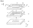
- FIG. 2 shows an exploded view of the resin multilayer substrate in the present embodiment.
- the resin multilayer substrate is made by stacking three resin layers 2 called L1, L2, and L3 in order from the top.
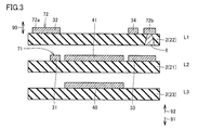
- FIG. 3 shows a cross-sectional view taken along the line III-III in FIG.
- the III-III line is displayed in the vicinity of the layer L1, but the III-III line means that not only the layer L1 but also the layers L1 to L3 are cut all at once.
- the first side 91 is the lower side
- the second side 92 is the upper side
- the conductor pattern is arranged on the upper surface of each layer, but this is only an example, This is not always true.
- the first side 91 may be the upper side
- the second side 92 may be the lower side
- a conductor pattern may be disposed on the lower surface of each layer.
- the auxiliary pattern 40 is disposed on the surface of the second side 92 of the resin layer 2 of the layer L3.
- a first conductor pattern 31, a third conductor pattern 33, and a first dummy pattern 41 are arranged on the surface of the second side 92 of the resin layer 2 of the layer L2.
- the first conductor pattern 31 and the third conductor pattern 33 are connected as shown in FIG. 2, and both are part of the conductor pattern 71.
- the auxiliary pattern 40 and the first dummy pattern 41 are both electrically independent conductor films. That is, neither the auxiliary pattern 40 nor the first dummy pattern 41 is electrically connected to other electrodes.
- the auxiliary pattern 40 is disposed at a position corresponding to the first dummy pattern 41.
- the second conductor pattern 32 and the fourth conductor pattern 34 are arranged on the surface of the second side 92 of the resin layer 2 of the layer L1. However, the second conductor pattern 32 and the fourth conductor pattern 34 are connected as shown in FIG. 2, and both are part of the conductor pattern 72.
- External connection electrodes 72a and 72b are also arranged on the surface of the second side 92 of the resin layer 2 of the layer L1.
- the external connection electrode 72 a is a part of the conductor pattern 72.
- the external connection electrode 72 b is an independent conductor film provided apart from the conductor pattern 72. In the layer L1, no conductor pattern is arranged in the region corresponding to the first dummy pattern 41 and is empty.
- the auxiliary pattern 40 is shifted to the second side 92 as compared with that before thermocompression bonding due to heat and pressure during thermocompression bonding.
- the surface on the second side 92 of the auxiliary pattern 40 is located on the second side 92 relative to the surface on the first side 91 of the first conductor pattern 31 and the third conductor pattern 33.
- the first dummy pattern 41 is also displaced to the second side 92 as compared to before the thermocompression bonding.
- the surface on the second side 92 of the first dummy pattern 41 is located on the second side 92 relative to the surface on the first side 91 of the second conductor pattern 32 and the fourth conductor pattern 34.
- the surface on the second side 92 of the first conductor pattern 31 and the third conductor pattern 33 is located on the second side 92 with respect to the surface on the first side 91 of the first dummy pattern 41.
- the auxiliary pattern 40 and The first dummy pattern 41 tends to shift to the second side 92.
- the conductor pattern 72 is disposed on the layer L1, and the conductor pattern 71 is disposed on the layer L2. Since these are in a positional relationship, the conductor patterns 71 and 72 are also connected to the second side during thermocompression bonding. It is difficult to shift to 92.
- the resin multilayer substrate 102 in the present embodiment has the same basic configuration as the resin multilayer substrate 101 described in the first embodiment, but further includes the following configuration.
- the resin multilayer substrate 102 in the present embodiment when the resin multilayer substrate 102 is viewed in a cross-sectional view in which the first conductor pattern 31, the second conductor pattern 32, and the first dummy pattern 41 are visible, that is, in FIG.
- a conductor pattern formed integrally with the conductor pattern 31 or formed separately from the first conductor pattern 31 appears at the same height as the first conductor pattern, and this is referred to as a third conductor pattern 33.
- a conductor pattern formed integrally with the second conductor pattern 32 or formed separately from the second conductor pattern 32 appears at the same height as the second conductor pattern 32, and this is the fourth.
- the conductor pattern 34 in the cross-sectional view, a part of the first side 91 of the first dummy pattern 41 is the first conductor pattern 31 and the third conductor pattern 33. It is sandwiched between the part of the second side 92 of the first dummy pattern 41 is sandwiched between the second conductor pattern 32 and the fourth conductor pattern 34.
- the resin multilayer substrate 102 in the present embodiment since the first dummy pattern 41 is arranged in the space between the two conductor patterns, the two conductor patterns are displaced toward the space between them during thermocompression bonding. Can be suppressed.
- the width of the first dummy pattern 41 in the sectional view is W1
- the length of the gap between the first conductor pattern 31 and the third conductor pattern 33 in the sectional view is W2, W1 ⁇ W2 / 2. It is preferable that By adopting this configuration, the first dummy pattern 41 can be brought closer to the first conductor pattern 31 and the third conductor pattern 33, and the effect of suppressing the displacement of the conductor pattern by the first dummy pattern 41 can be enhanced. it can.
- the resin multilayer substrate includes a coil conductor having a winding axis parallel to the stacking direction 90, and includes a first conductor pattern 31, a second conductor pattern 32, a third conductor pattern 33, and a first conductor pattern 33.
- Each of the four conductor patterns 34 is preferably a part of the coil conductor.
- the first conductor pattern 31 or the like is a part of the coil conductor, the first dummy pattern 41 is arranged in the center surrounded by these conductor patterns, thereby effecting undesired displacement at the time of thermocompression bonding. Can be suppressed.
- the resin multilayer substrate includes a coil conductor having a winding direction as a winding axis, and both the first conductor pattern and the second conductor pattern are part of the coil conductor.
- the first dummy pattern is arranged, thereby effectively preventing undesired displacement during thermocompression bonding. Can be suppressed.
- the presence of the third conductor pattern 33 and the fourth conductor pattern 34 is not essential.
- the method for manufacturing the resin multilayer substrate includes the second conductor pattern 32 on the second side of the first resin layer 21 having the first conductor pattern 31 on the surface of the second side 92.
- the step of obtaining the laminate includes the first dummy pattern 41 arranged in a region different from the region covered by the first conductor pattern 31 on the surface of the second side 92 of the first resin layer 21.
- the third side This is done by stacking the resin layer 23, the first resin layer 21 and the second resin layer 22 in this order.
- the layers L1 to L3 as shown in FIG. 3 are stacked and thermocompression bonded, but instead, as shown in FIG.
- the layers L1 to L4 may be stacked and thermocompression bonded.
- the first conductor pattern 31 and the third conductor pattern 33 are arranged in the layer L3. There is a space between the first conductor pattern 31 and the third conductor pattern 33.
- the first dummy pattern 41 is not disposed on the layer L3 but on the layer L2 adjacent to the second side 92 of the layer L3. Only the first dummy pattern 41 is disposed in the layer L2.
- the method for manufacturing the resin multilayer substrate includes the second conductor pattern 32 on the second side 92 of the first resin layer 21 having the first conductor pattern 31 on the surface of the second side 92.
- the step of obtaining the laminate is performed by disposing the fourth resin layer 24 between the first resin layer 21 and the second resin layer 22, and the fourth resin layer 24 is The first dummy pattern 41 is provided on the second side 92 surface.
- the resin multilayer substrate 102 see FIG. 4 in the present embodiment can be obtained.
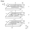
- FIG. 6 shows an exploded view of the resin multilayer substrate in the present embodiment.
- the resin multilayer substrate is made by stacking three resin layers 2 called L1, L2, and L3 in order from the top.
- a conductor pattern 72 is disposed on the upper surface of the layer L1 so as to form a part of a coil.
- the first dummy pattern 41 is disposed inside the conductor pattern 72.
- On the upper surface of the layer L3, a conductor pattern 73 forming a part of a coil is disposed.
- the auxiliary pattern 40 is disposed inside the conductor pattern 73.
- the auxiliary pattern 40 occupies an area corresponding to the first dummy pattern 41.
- a conductor pattern 71 is disposed on the upper surface of the layer L2 so as to form part of the coil.
- An opening 3 is provided inside the conductor pattern 71.
- the opening 3 is provided in a region corresponding to the auxiliary pattern 40 and the first dummy pattern 41.
- FIG. 7 shows a cross-sectional view of the process of laminating and thermocompression bonding these layers L1 to L3. Pressurization is performed using the molds 11 and 12 arranged so as to face each other.
- the mold 11 is provided with a convex portion 11a.
- the mold 12 is provided with a convex portion 12a.
- a resin multilayer substrate 103 shown in FIG. 8 is obtained. Concave portions are respectively formed at locations corresponding to the convex portions 11a and 12a.
- the auxiliary pattern 40 and the first dummy pattern 41 at the center are displaced from the original position in the stacking direction.
- the one on the second side 92 is called the first dummy pattern 41
- the one on the first side 91 is called the auxiliary pattern 40.
- both the auxiliary pattern 40 and the first dummy pattern 41 function in the same manner in suppressing the resin flow.
- the method for manufacturing the resin multilayer substrate in the present embodiment is the second side 92 of the first resin layer 21 having the first conductive pattern 31 on the surface of the second side 92, and the second Including a step of stacking a plurality of resin layers 2 including a step of stacking the second resin layer 22 having the conductor pattern 32 on the surface of the second side 92, and heating and pressurizing the stack.
- Including the step of thermocompression-bonding the laminate, and the step of obtaining the laminate includes a first dummy on the surface of the second side 92 of one resin layer 2 of the first resin layer 21 and the second resin layer 22.
- the pattern 41 is arranged, and the other resin layer 2 is performed in a state where the opening 3 or the notch is provided in a region corresponding to the first dummy pattern 41.
- the opening 3 is provided in the resin layer 2 of the layer L2, and the first dummy pattern 41 is disposed in the resin layer 2 of the layer L1, but instead of the layer L1,
- the opening part 3 may be provided in the resin layer 2, and the 1st dummy pattern 41 may be arrange
- the position of the dummy pattern can be adjusted to a desired position in the stacking direction in the resin multilayer substrate by providing openings or notches in some resin layers. . As shown in the present embodiment, the position of the dummy pattern can also be adjusted to a desired position in the stacking direction in the resin multilayer substrate by providing a convex portion on the mold.
- the thermocompression bonding step is preferably performed by arranging a first member that can follow the unevenness of the pressed object on the first side 91 or the second side 92 of the laminate.
- a mold having a convex portion is used as the first member.
- the first member may have a configuration other than this.
- the first member preferably includes a cushion material. It is preferable that a 1st member contains a metal mold
- the aggregate resin layer 200 is a large resin layer in which a plurality of the resin layers 2 shown in FIG. 2 are combined and arranged in a matrix.
- the aggregate resin layer 200 having a size corresponding to nine resin multilayer substrates is shown as an example, but the aggregate resin layer 200 may correspond to a number of resin multilayer substrates other than nine.
- the aggregate resin layer 200 may have a large area corresponding to a larger number of resin multilayer substrates.
- a set auxiliary pattern 450 is disposed on the surface of the second side 92 of the set resin layer 200 of the layer L3.
- a plurality of collective auxiliary patterns 450 are arranged in parallel.
- the collective auxiliary pattern 450 includes a main line portion that is continuous in a strip shape and branch portions that protrude from the main line portion on both sides.
- a plurality of conductor patterns 71 are arranged in a matrix on the surface of the second side 92 of the aggregate resin layer 200 of the layer L2.
- a collective dummy pattern 460 is arranged so as to separate the rows of conductor patterns 71.
- the collective dummy pattern 460 has a main line portion continuous in a strip shape and branch portions protruding from the main line portion on both sides.
- a plurality of conductor patterns 72 are arranged in a matrix on the surface of the second side 92 of the aggregate resin layer 200 of the layer L1.
- a part of the conductor pattern 72 is an external connection electrode 72a.
- the external connection electrode 72b is disposed apart from the conductor pattern 72.
- the layers L1, L2, and L3 are stacked and thermocompression bonded, as shown in FIG.
- the set dummy pattern 460 When pressed by the set auxiliary pattern 450, the set dummy pattern 460 is shifted slightly to the second side 92 from the same height as the conductor pattern 72. What is thermocompression bonded in this way is cut into sizes of individual resin multilayer substrates. In this case, for example, it is cut along the cutting line 13.
- An individual resin multilayer substrate obtained in this way is shown in an exploded view as shown in FIG.
- a material obtained by cutting the aggregate resin layer 200 corresponds to the resin layer 2.
- the dummy pattern 46 is formed by cutting the collective dummy pattern 460 along the cutting line 13.
- the auxiliary pattern 45 is formed by cutting the collective auxiliary pattern 450 along the cutting line 13. In FIG.
- the shift in the stacking direction of the dummy patterns 45 and 46 is not expressed.
- the dummy pattern 46 does not continue to be at the same height as the conductor pattern 71 during thermocompression bonding, and the dummy pattern 46 may be displaced in the stacking direction as compared with the conductor pattern 71.
- the manufacturing method of the resin multilayer substrate in the present embodiment basically includes the same steps as the manufacturing method described in the second embodiment, but differs in the following points.
- an aggregate laminate is obtained by performing collectively using an aggregate resin layer having a size corresponding to a plurality of resin multilayer substrates.
- the assembly laminate is subjected to thermocompression by collectively heating and pressing, and after the thermocompression, the assembly laminate is divided into sizes corresponding to individual resin multilayer substrates. including.
- the obtained individual resin multilayer substrate has a dummy pattern outside the conductor pattern, it is possible to suppress a deviation in the plane direction when compared between conductor patterns arranged in different layers included in the laminate. it can.
- the step of dividing includes a step of cutting the first dummy pattern included in the assembly stack from a pattern having a larger size. If it does in this way, the 1st dummy pattern arrange
- the manufacturing method of the resin multilayer substrate in this case can be expressed as follows, for example.
- the method for producing a resin multilayer substrate is a method for producing a resin multilayer substrate including a state in which a plurality of resin layers mainly composed of a thermoplastic resin are laminated, wherein the lamination direction is aligned with the vertical direction.
- the resin multilayer substrate is dispersed and arranged at two or more heights.
- the plurality of trees including Including a step of obtaining a laminate by stacking layers and a step of thermocompression-bonding the laminate by heating and pressurizing the laminate, and the step of obtaining the laminate includes the first resin layer and the first layer A first dummy pattern formed of the first material is disposed in one of the two resin layers, and an opening or a notch is provided in a region corresponding to the first dummy pattern in the other resin layer. And a step of cutting the region including the first dummy pattern after the step of thermocompression bonding.
- a plurality of aggregate resin layers 200 are laminated as shown in FIG.
- the aggregate resin layer 200 shown here is similar to that shown in the fourth embodiment, but differs from the one shown in the fourth embodiment in the following points.
- auxiliary patterns 40 are disposed on the surface of the second side 92 of the collective resin layer 200 of the layer L3.
- the plurality of auxiliary patterns 40 are arranged at regular intervals in a matrix.
- each auxiliary pattern 40 has a rectangular outer shape.
- a plurality of first dummy patterns 41 are disposed on the surface of the second side 92 of the assembly resin layer 200 of the layer L2. Each of the first dummy patterns 41 is disposed at a position corresponding to the auxiliary pattern 40.
- the layers L1, L2, and L3 are stacked and thermocompression bonded as shown in FIG.
- the set auxiliary pattern 450 When pressed by the set auxiliary pattern 450, the set dummy pattern 460 is shifted slightly to the second side 92 from the same height as the conductor pattern 72. What is thermocompression bonded in this way is cut into sizes of individual resin multilayer substrates.
- the conductor pattern can be sandwiched between the two dummy patterns. Thereby, the shift
- the resin multilayer substrate obtained in the present embodiment has the following configuration.
- the resin multilayer substrate according to the present embodiment includes a second dummy pattern formed of the first material at the same height as the first dummy pattern 41, and the second dummy pattern includes the first conductor pattern 31 and the first dummy pattern.
- the first and second dummy patterns 41 and 32 are not electrically connected to any of the two-conductor patterns 32, and the first and second dummy patterns 41 and 32 are viewed in a cross-sectional view. Are arranged so as to sandwich at least one of them.
- the “second dummy pattern” is, for example, any dummy pattern obtained by being cut out from the collective dummy pattern 460.
- the first conductor pattern 31 is sandwiched between the first dummy pattern 41 and the second dummy pattern in a certain place. In some other place, the second conductor pattern 32 is sandwiched between the first dummy pattern 41 and the second dummy pattern.
- Embodiment 6 With reference to FIG. 15, the manufacturing method of the resin multilayer substrate in Embodiment 6 based on this invention is demonstrated. Here, the region corresponding to one resin multi-layer substrate is shown, but it is also possible to manufacture a plurality of resin multi-layer substrates at once using an aggregate resin layer as in the fourth and fifth embodiments. Good.
- At least one of the first dummy pattern 41 and the second dummy pattern includes a frame-like portion when viewed from a direction perpendicular to the resin layer.
- the “frame-shaped portion” may be a frame shape that is completely closed loop, but a frame having one or more breaks, such as the dummy pattern 48 shown as the layer L2 in FIG. It may be a shape.
- the dummy pattern 48 corresponds to the second dummy pattern.
- the dummy pattern 48 has a cut on one side.
- one end of the conductor pattern 71 enters the break of the dummy pattern 48.
- the present invention is not limited to this configuration.
- a configuration in which one end of the conductor pattern 71 passes through the cut of the dummy pattern 48 and further extends to the outside of the frame may be employed.
- the dummy pattern 48 may be configured to have two or more cuts.
- the dummy pattern 47 is arranged so as to occupy an area corresponding to the dummy pattern 48 of the layer L2.
- the conductor pattern at the time of thermocompression bonding is surrounded all around the conductor pattern 71. Displacement can be suppressed.
Landscapes
- Engineering & Computer Science (AREA)
- Microelectronics & Electronic Packaging (AREA)
- Manufacturing & Machinery (AREA)
- Production Of Multi-Layered Print Wiring Board (AREA)
Abstract
樹脂多層基板(101)は、第1材料で形成された第1ダミーパターン(41)を備え、第1ダミーパターン(41)は、第1の側(91)を向く第1面(41a)と、第2の側(92)を向く第2面(41b)とを有し、第1導体パターン(31)および第2導体パターン(32)のいずれに対しても電気的に接続されておらず、第1導体パターン(31)の第2の側(92)の面のうち最も第2の側(92)にある点よりも第1面(41a)の方が第1の側(91)にあり、第2導体パターン(32)の第1の側(91)の面のうち最も第1の側(91)にある点よりも第2面(41b)の方が第2の側(92)にある。
Description
本発明は、樹脂多層基板およびその製造方法に関するものである。
巻回形の線状導体が形成された熱可塑性樹脂からなる複数の絶縁性基材を加熱圧着することによって前記巻回形の線状導体でコイルを構成する場合において、前記熱可塑性樹脂よりも流動性が低い部材を、前記巻回形の線状導体に囲まれる領域に配置することが、国際公開WO2015/129601号(特許文献1)に記載されている。
積層体の中で、積層方向に互いに隣接する2つの樹脂層に注目し、これらを以下「第1層」および「第2層」と呼ぶこととする。第1層および第2層にはそれぞれ巻回形の線状導体が配置されているものとする。特許文献1に記載されているように、第1層および第2層の各々において、巻回形の線状導体に囲まれる領域に流動性が低い部材を配置した場合、第1層および第2層の個別の同一層内での導体パターン同士の相対的なずれは抑制できるかもしれない。すなわち、巻回形の線状導体はそのままの姿を維持しやすい。しかし、第1層と第2層との間で見比べた場合、面方向の相対的なずれはほとんど抑制されない。すなわち、積層体を一体化するための熱圧着を施した際に、第1層内の導体パターン同士の組合せは互いの相対的な位置関係を維持し、第2層内の導体パターン同士の組合せは互いの相対的な位置関係を維持している可能性があるものの、第1層と第2層との間では導体パターンの位置が面方向に互いにずれているという状態が起こるおそれがある。
そこで、本発明は、積層体に含まれる異なる層に配置された導体パターン同士の間で比較したときの面方向のずれを抑制することができる樹脂多層基板およびその製造方法を提供することを目的とする。
上記目的を達成するため、本発明に基づく樹脂多層基板は、熱可塑性樹脂を主材料とする複数の樹脂層が積層された状態のものを含む樹脂多層基板であって、積層方向が上下方向と一致する姿勢にして上記樹脂多層基板を見たときの上側および下側のうち一方を第1の側とし、他方を第2の側としたとき、上記樹脂多層基板は、2通り以上の高さに分散して配置され、第1材料で形成された複数の導体パターンを内部に含み、上記複数の導体パターンのうち、上記積層方向に互いに離隔しつつ積層方向に並ぶ2つの導体パターンを、上記第1の側から順に第1導体パターンおよび第2導体パターンと呼ぶこととすると、上記樹脂多層基板は、上記第1材料で形成された第1ダミーパターンを備え、上記第1ダミーパターンは、上記第1の側を向く第1面と、上記第2の側を向く第2面とを有し、上記第1導体パターンおよび上記第2導体パターンのいずれに対しても電気的に接続されておらず、上記第1導体パターンの上記第2の側の面のうち最も上記第2の側にある点よりも上記第1面の方が上記第1の側にあり、上記第2導体パターンの上記第1の側の面のうち最も上記第1の側にある点よりも上記第2面の方が上記第2の側にある。
本発明によれば、側方から見たときに、積層方向に並ぶ複数の導体パターンと重なるように、第1ダミーパターンが配置されているので、積層体に含まれる異なる層に配置された導体パターン同士の間で比較したときの面方向のずれを抑制することができる。
図面において示す寸法比は、必ずしも忠実に現実のとおりを表しているとは限らず、説明の便宜のために寸法比を誇張して示している場合がある。以下の説明において、上または下の概念に言及する際には、絶対的な上または下を意味するものではなく、図示された姿勢の中での相対的な上または下を意味するものである。
(実施の形態1)
図1を参照して、本発明に基づく実施の形態1における樹脂多層基板について説明する。本実施の形態における樹脂多層基板の断面図を図1に示す。図1では、樹脂層同士の境目が表示されていないが、実際には、樹脂多層基板は、複数の樹脂層を積み重ねて熱圧着により一体化したものである。詳細に観察することにより元の樹脂層同士の境界を確認することができる。
図1を参照して、本発明に基づく実施の形態1における樹脂多層基板について説明する。本実施の形態における樹脂多層基板の断面図を図1に示す。図1では、樹脂層同士の境目が表示されていないが、実際には、樹脂多層基板は、複数の樹脂層を積み重ねて熱圧着により一体化したものである。詳細に観察することにより元の樹脂層同士の境界を確認することができる。
本実施の形態における樹脂多層基板101は、熱可塑性樹脂を主材料とする複数の樹脂層が積層された状態のものを含む樹脂多層基板であって、積層方向90が上下方向と一致する姿勢にして樹脂多層基板101を見たときの上側および下側のうち一方を第1の側91とし、他方を第2の側92としたとき、樹脂多層基板101は、2通り以上の高さに分散して配置され、第1材料で形成された複数の導体パターンを内部に含み、複数の導体パターンのうち、積層方向90に互いに離隔しつつ積層方向90に並ぶ2つの導体パターンを、第1の側91から順に第1導体パターン31および第2導体パターン32と呼ぶこととすると、樹脂多層基板101は、前記第1材料で形成された第1ダミーパターン41を備え、第1ダミーパターン41は、第1の側91を向く第1面41aと、第2の側92を向く第2面41bとを有し、第1導体パターン31および第2導体パターン32のいずれに対しても電気的に接続されておらず、第1導体パターン31の第2の側92の面のうち最も第2の側92にある点よりも第1面41aの方が第1の側91にあり、第2導体パターン32の第1の側91の面のうち最も第1の側91にある点よりも第2面41bの方が第2の側92にある。
ここでは、第1導体パターン31と第2導体パターン32とが樹脂多層基板101の内部で平行に配置されているが、平行であるとは限らず、多少傾いていてもよい。また、第1導体パターン31および第2導体パターン32は、均一な厚みを有するとは限らず、厚みが異なる部分を有していてもよい。樹脂多層基板101の内部に含まれる複数の導体パターンは、各樹脂層のいずれの面に配置されていてもよい。導体パターンは、各樹脂層のいずれかの面に配置され、これらの複数の樹脂層が積層されることによって全体として樹脂多層基板が形成されていればよい。
本実施の形態では、第1ダミーパターンは、側方から見たときに、積層方向に並ぶ複数の導体パターンと重なるように配置されているので、積層体に含まれる異なる層に配置された導体パターン同士の間で比較したときの面方向のずれを抑制することができる。第1導体パターン31と第2導体パターン32とは、積層方向90から見たときに少なくとも一部が重なる位置関係であることが好ましい。
第1材料は銅を含むことが好ましい。この構成を採用することにより、導体パターンにより樹脂多層基板内に導電性に優れた配線を形成することができる。このことは、以下の各実施の形態においても同様にあてはまる。
(実施の形態2)
図2~図4を参照して、本発明に基づく実施の形態2における樹脂多層基板について説明する。本実施の形態における樹脂多層基板の分解図を図2に示す。この例では、樹脂多層基板は、上から順にL1,L2,L3と呼ばれる3つの樹脂層2を積み重ねて作られている。図2におけるIII-III線に関する矢視断面図を図3に示す。図2では、層L1の近傍にIII-III線が表示されているが、III-III線は、層L1のみならず層L1~L3を一括して切ることを意味する。ここでは、第1の側91が下側であり、第2の側92が上側であって、各層の上面に導体パターンが配置されているものとして説明するが、これはあくまで一例であって、このとおりとは限らない。たとえば第1の側91が上側であり、第2の側92が下側であって、各層の下面に導体パターンが配置された構成であってもよい。
図2~図4を参照して、本発明に基づく実施の形態2における樹脂多層基板について説明する。本実施の形態における樹脂多層基板の分解図を図2に示す。この例では、樹脂多層基板は、上から順にL1,L2,L3と呼ばれる3つの樹脂層2を積み重ねて作られている。図2におけるIII-III線に関する矢視断面図を図3に示す。図2では、層L1の近傍にIII-III線が表示されているが、III-III線は、層L1のみならず層L1~L3を一括して切ることを意味する。ここでは、第1の側91が下側であり、第2の側92が上側であって、各層の上面に導体パターンが配置されているものとして説明するが、これはあくまで一例であって、このとおりとは限らない。たとえば第1の側91が上側であり、第2の側92が下側であって、各層の下面に導体パターンが配置された構成であってもよい。
層L3の樹脂層2の第2の側92の面には、補助パターン40が配置されている。層L2の樹脂層2の第2の側92の面には、第1導体パターン31、第3導体パターン33および第1ダミーパターン41が配置されている。ただし、第1導体パターン31および第3導体パターン33は、図2に示すようにつながっており、いずれも導体パターン71の一部である。
補助パターン40および第1ダミーパターン41は、いずれも電気的に独立した導体膜である。すなわち、補助パターン40および第1ダミーパターン41は、いずれも他の電極と電気的に接続されていない。補助パターン40は第1ダミーパターン41に対応する位置に配置されている。
層L1の樹脂層2の第2の側92の面には、第2導体パターン32および第4導体パターン34が配置されている。ただし、第2導体パターン32および第4導体パターン34は、図2に示すようにつながっており、いずれも導体パターン72の一部である。層L1の樹脂層2の第2の側92の面には、外部接続電極72a,72bも配置されている。外部接続電極72aは、導体パターン72の一部である。外部接続電極72bは、導体パターン72から離隔して設けられた独立した導体膜である。層L1においては、第1ダミーパターン41に対応する領域には何も導体パターンは配置されておらず空いている。
図3に示す層L1,L2,L3を積み重ねて熱圧着することによって、図4に示す樹脂多層基板102が得られる。熱圧着時の熱および圧力により補助パターン40は熱圧着前に比べて第2の側92にずれている。その結果、補助パターン40の第2の側92の面は、第1導体パターン31および第3導体パターン33の第1の側91の面よりも第2の側92に位置している。熱圧着時に補助パターン40に押されることによって、第1ダミーパターン41も熱圧着前に比べて第2の側92にずれている。その結果、第1ダミーパターン41の第2の側92の面は、第2導体パターン32および第4導体パターン34の第1の側91の面よりも第2の側92に位置している。第1導体パターン31および第3導体パターン33の第2の側92の面は、第1ダミーパターン41の第1の側91の面よりも第2の側92に位置している。図3に示すように、層L1は、補助パターン40および第1ダミーパターン41と重なる位置に導体パターンを有していないので、層L1,L2,L3を積み重ねて熱圧着したときには補助パターン40および第1ダミーパターン41は第2の側92にずれやすい。層L1には導体パターン72が配置されており、層L2には導体パターン71が配置され、これらは重なる位置関係にあるので、導体パターン71,72は、熱圧着の際にも第2の側92にはずれにくい。
本実施の形態における樹脂多層基板102は、実施の形態1で説明した樹脂多層基板101と基本的な構成は共通するが、さらに以下の構成を備える。本実施の形態における樹脂多層基板102においては、第1導体パターン31、第2導体パターン32および第1ダミーパターン41が見えるような断面図すなわち図4で樹脂多層基板102を見たとき、第1導体パターン31と一体的に形成された、または、第1導体パターン31とは別箇に形成された導体パターンが前記第1導体パターンと同じ高さに表れ、これを第3導体パターン33と呼ぶこととし、第2導体パターン32と一体的に形成された、または、第2導体パターン32とは別箇に形成された導体パターンが第2導体パターン32と同じ高さに表れ、これを第4導体パターン34と呼ぶこととしたとき、前記断面図において、第1ダミーパターン41の第1の側91の一部は、第1導体パターン31と第3導体パターン33との間に挟まれており、第1ダミーパターン41の第2の側92の一部は、第2導体パターン32と第4導体パターン34との間に挟まれている。
本実施の形態における樹脂多層基板102によれば、2つの導体パターン同士の間のスペースに第1ダミーパターン41が配置されているので、熱圧着時に2つの導体パターンが間のスペースに向かって変位することを抑制することができる。
さらに、前記断面図における第1ダミーパターン41の幅をW1とし、前記断面図における第1導体パターン31と第3導体パターン33との間の間隙の長さをW2とすると、W1≧W2/2であることが好ましい。この構成を採用することにより、第1ダミーパターン41を第1導体パターン31および第3導体パターン33に対して近づけることができ、導体パターンの変位に対する第1ダミーパターン41による抑止効果を高めることができる。
図2に示すように、前記樹脂多層基板は、積層方向90に平行な巻回軸を有するコイル導体を含んでおり、第1導体パターン31、第2導体パターン32、第3導体パターン33および第4導体パターン34はいずれも前記コイル導体の一部であることが好ましい。このように第1導体パターン31などがコイル導体の一部である場合、これらの導体パターンに囲まれる中央に第1ダミーパターン41が配置されることによって、熱圧着時の不所望な変位を効果的に抑制することができる。
前記樹脂多層基板は、積層方向を巻回軸とするコイル導体を含んでおり、前記第1導体パターンおよび前記第2導体パターンはいずれも前記コイル導体の一部であることが好ましい。このように、第1導体パターンおよび第2導体パターンの2つがコイル導体の一部である場合においても、第1ダミーパターンが配置されることによって、熱圧着時の不所望な変位を効果的に抑制することができる。この場合、第3導体パターン33および第4導体パターン34の存在は必須ではない。
本実施の形態で示した製造方法は、以下のように表現することができる。この樹脂多層基板の製造方法は、図3に示すように、第1導体パターン31を第2の側92の面に有する第1樹脂層21の第2の側に、第2導体パターン32を第2の側92の面に有する第2樹脂層22を重ねる工程を含みつつ複数の樹脂層2を積み重ねることによって積層体を得る工程と、前記積層体を加熱および加圧することによって前記積層体を熱圧着させる工程とを含む。前記積層体を得る工程は、第1樹脂層21の第2の側92の面の第1導体パターン31が覆う領域とは別の領域に第1ダミーパターン41が配置された状態で、第1樹脂層21の第1の側91に、第1ダミーパターン41に対応する領域に延在する補助パターン40を第2の側92の面に有する第3樹脂層23を配置した状態で、第3樹脂層23、第1樹脂層21および第2樹脂層22をこの順に積み重ねることによって行なわれる。このような樹脂多層基板の製造方法を実施することにより、たとえば本実施の形態における樹脂多層基板102(図4参照)を得ることができる。
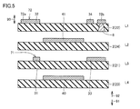
なお、本実施の形態では、図4に示す樹脂多層基板102を得るために、図3に示すような層L1~L3を積み重ねて熱圧着したが、これに代えて、図5に示すような層L1~L4を積み重ねて熱圧着することとしてもよい。図5に示した例では、層L3には、第1導体パターン31および第3導体パターン33が配置されている。第1導体パターン31と第3導体パターン33との間は空いている。第1ダミーパターン41は、層L3ではなく、層L3の第2の側92に隣接する層L2に配置されている。層L2には、第1ダミーパターン41のみが配置されている。
この変形例としての製造方法は、以下のように表現することができる。この樹脂多層基板の製造方法は、図5に示すように、第1導体パターン31を第2の側92の面に有する第1樹脂層21の第2の側92に、第2導体パターン32を第2の側92の面に有する第2樹脂層22を重ねる工程を含みつつ複数の樹脂層2を積み重ねることによって積層体を得る工程と、前記積層体を加熱および加圧することによって前記積層体を熱圧着させる工程とを含み、前記積層体を得る工程は、第1樹脂層21と第2樹脂層22との間に第4樹脂層24を配置することによって行なわれ、第4樹脂層24は、第1ダミーパターン41を第2の側92の面に有する。このような樹脂多層基板の製造方法を実施することによっても、たとえば本実施の形態における樹脂多層基板102(図4参照)を得ることができる。
(実施の形態3)
図6~図8を参照して、本発明に基づく実施の形態3における樹脂多層基板について説明する。本実施の形態における樹脂多層基板の分解図を図6に示す。この例では、樹脂多層基板は、上から順にL1,L2,L3と呼ばれる3つの樹脂層2を積み重ねて作られている。層L1の上面には、コイルの一部をなすように導体パターン72が配置されている。導体パターン72の内側に第1ダミーパターン41が配置されている。層L3の上面には、コイルの一部をなす導体パターン73が配置されている。導体パターン73の内側に補助パターン40が配置されている。補助パターン40は、第1ダミーパターン41に対応する領域を占めている。層L2の上面には、コイルの一部をなすように導体パターン71が配置されている。導体パターン71の内側には開口部3が設けられている。開口部3は、補助パターン40および第1ダミーパターン41に対応する領域に設けられている。これらの層L1~L3を積層して熱圧着させる工程の様子を断面図で示すと図7のようになる。互いに対向するように配置された金型11,12を使用して加圧が行なわれる。金型11には凸部11aが設けられている。金型12には凸部12aが設けられている。
図6~図8を参照して、本発明に基づく実施の形態3における樹脂多層基板について説明する。本実施の形態における樹脂多層基板の分解図を図6に示す。この例では、樹脂多層基板は、上から順にL1,L2,L3と呼ばれる3つの樹脂層2を積み重ねて作られている。層L1の上面には、コイルの一部をなすように導体パターン72が配置されている。導体パターン72の内側に第1ダミーパターン41が配置されている。層L3の上面には、コイルの一部をなす導体パターン73が配置されている。導体パターン73の内側に補助パターン40が配置されている。補助パターン40は、第1ダミーパターン41に対応する領域を占めている。層L2の上面には、コイルの一部をなすように導体パターン71が配置されている。導体パターン71の内側には開口部3が設けられている。開口部3は、補助パターン40および第1ダミーパターン41に対応する領域に設けられている。これらの層L1~L3を積層して熱圧着させる工程の様子を断面図で示すと図7のようになる。互いに対向するように配置された金型11,12を使用して加圧が行なわれる。金型11には凸部11aが設けられている。金型12には凸部12aが設けられている。
図7に示すように、積み重ねた層L1~L3に対して加熱および加圧が行なわれると、図8に示す樹脂多層基板103が得られる。凸部11a,12aに対応する箇所にはそれぞれ凹部が形成されている。中央部の補助パターン40および第1ダミーパターン41は、それぞれ当初の位置から積層方向にずれている。この例では、図8における中央の2枚の導体パターンのうち第2の側92にあるものを第1ダミーパターン41と呼び、第1の側91にあるものを補助パターン40と呼んでいるが、あくまで説明の便宜上そのように呼び分けているに過ぎず、実際には、補助パターン40も第1ダミーパターン41も、樹脂の流動を抑制する上では同様に作用する。
本実施の形態で示した製造方法は、以下のように表現することができる。本実施の形態における樹脂多層基板の製造方法は、図7に示すように、第1導体パターン31を第2の側92の面に有する第1樹脂層21の第2の側92に、第2導体パターン32を第2の側92の面に有する第2樹脂層22を重ねる工程を含みつつ複数の樹脂層2を積み重ねることによって積層体を得る工程と、前記積層体を加熱および加圧することによって前記積層体を熱圧着させる工程とを含み、前記積層体を得る工程は、第1樹脂層21および第2樹脂層22のうち一方の樹脂層2の第2の側92の面に第1ダミーパターン41が配置され、他方の樹脂層2には第1ダミーパターン41に対応する領域に開口部3または切欠きが設けられた状態で行なわれる。
図6および図7で示した例では、層L2の樹脂層2に開口部3を設け、層L1の樹脂層2に第1ダミーパターン41が配置されていたが、この代わりに、層L1の樹脂層2に開口部3を設け、層L2の樹脂層2に第1ダミーパターン41が配置されていてもよい。いずれの場合であっても、開口部に代えて切欠きを設けておくこととしてもよい。
本実施の形態で示したように、一部の樹脂層に開口部または切欠きを設けておくことによっても、ダミーパターンの位置を樹脂多層基板内の積層方向の所望の位置に整えることができる。本実施の形態で示したように、金型に凸部を設けることによっても、ダミーパターンの位置を樹脂多層基板内の積層方向の所望の位置に整えることができる。
前記熱圧着させる工程は、前記積層体の第1の側91または第2の側92に、被加圧物の凹凸に追従することができる第1部材を配置して行なわれることが好ましい。本実施の形態では、第1部材として凸部を有する金型を用いていた。第1部材は、これ以外の構成であってもよい。たとえば第1部材は、クッション材を含むことが好ましい。第1部材は、金型と、金型と積層体との間に配置されたクッション材とを含むことが好ましい。クッション材を含むものであることにより、加圧時には積層体の表面に存在する凹凸に沿って第1部材が変形し、積層体に対して均等に近い加圧をすることができる。
(実施の形態4)
図9~図11を参照して、本発明に基づく実施の形態4における樹脂多層基板の製造方法について説明する。本実施の形態では、複数の樹脂多層基板を一括して得ることができる。
図9~図11を参照して、本発明に基づく実施の形態4における樹脂多層基板の製造方法について説明する。本実施の形態では、複数の樹脂多層基板を一括して得ることができる。
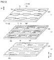
本実施の形態における樹脂多層基板の製造方法では、図9に示すように、複数の集合樹脂層200を積層する。集合樹脂層200とは、図2に示した樹脂層2を複数合わせてマトリックス状に配列したような大判の樹脂層である。ここでは、一例として樹脂多層基板9個分に相当するサイズの集合樹脂層200を示しているが、集合樹脂層200は、9以外の数の樹脂多層基板に相当するものであってもよい。集合樹脂層200は、より多くの数の樹脂多層基板に相当する広い面積のものであってもよい。
層L3の集合樹脂層200の第2の側92の面には、集合補助パターン450が配置されている。複数の集合補助パターン450が平行に配置されている。集合補助パターン450は、帯状に連なる幹線部分とこの幹線部分から両脇に突出する枝部分とを有する。
層L2の集合樹脂層200の第2の側92の面には、複数の導体パターン71がマトリックス状に配置されている。導体パターン71の列同士を隔てるように集合ダミーパターン460が配置されている。集合ダミーパターン460は、帯状に連なる幹線部分とこの幹線部分から両脇に突出する枝部分とを有する。
層L1の集合樹脂層200の第2の側92の面には、複数の導体パターン72がマトリックス状に配置されている。導体パターン72の一部は外部接続電極72aとなっている。個々の樹脂多層基板に対応する領域内においては、導体パターン72から離隔して外部接続電極72bが配置されている。
層L1,L2,L3を積み重ねて熱圧着させることにより、図10に示すようになる。集合補助パターン450に押されて集合ダミーパターン460は導体パターン72と同じ高さからやや第2の側92にずれる。こうして熱圧着させたものを個々の樹脂多層基板のサイズに切り分ける。この際には、たとえば切断線13で切り分けられる。こうして得られる個別の樹脂多層基板を分解図で示すと図11のようになる。集合樹脂層200を切り分けたものは、樹脂層2に相当する。集合ダミーパターン460を切断線13で切り分けることによってダミーパターン46が形成される。集合補助パターン450を切断線13で切り分けることによって補助パターン45が形成される。図11では、ダミーパターン45,46の積層方向に関するずれは表現されていない。たとえば実際には、熱圧着の際に、ダミーパターン46は導体パターン71と同じ高さにあり続けるわけではなく、ダミーパターン46は導体パターン71に比べて積層方向にずれうる。
本実施の形態における樹脂多層基板の製造方法は、基本的には実施の形態2で説明した製造方法と同様の工程を備えているが、以下の点で異なる。本実施の形態における樹脂多層基板の製造方法は、前記積層体を得る工程では、複数の樹脂多層基板に対応するサイズの集合樹脂層を用いて一括して行なうことによって集合積層体を得、前記熱圧着する工程では、前記集合積層体を一括して加熱および加圧することによって熱圧着させ、前記熱圧着させる工程の後に、前記集合積層体を個別の樹脂多層基板に対応するサイズに分断する工程を含む。
本実施の形態では、複数の樹脂多層基板を一括して製造することができるので、生産効率を上げることができる。得られる個々の樹脂多層基板は、導体パターンの外側にダミーパターンを有するので、積層体に含まれる異なる層に配置された導体パターン同士の間で比較したときの面方向のずれを抑制することができる。
図10に示したように、前記分断する工程は、前記集合積層体に含まれる前記第1ダミーパターンをより大きなサイズのパターンから切り分ける工程を含むことが好ましい。このようにすれば、各樹脂多層基板に配置される第1ダミーパターンを効率良く形成することができる。
集合積層体から個々の樹脂多層基板を切り分ける工程においては、ダミーパターンおよび補助パターンが製品に残らないように切り分けることとしてもよい。この場合の樹脂多層基板の製造方法は、たとえば以下のように表現することができる。樹脂多層基板の製造方法は、熱可塑性樹脂を主材料とする複数の樹脂層が積層された状態のものを含む樹脂多層基板の製造方法であって、積層方向が上下方向と一致する姿勢にして前記樹脂多層基板を見たときの上側および下側のうち一方を第1の側とし、他方を第2の側としたとき、前記樹脂多層基板は、2通り以上の高さに分散して配置され、第1材料で形成された複数の導体パターンを内部に含み、前記複数の導体パターンのうち、前記積層方向に互いに離隔しつつ積層方向に並ぶ2つの導体パターンを、前記第1の側から順に第1導体パターンおよび第2導体パターンと呼ぶこととすると、前記第1導体パターンを有する第1樹脂層の前記第2の側に、前記第2導体パターンを有する第2樹脂層を重ねる工程を含みつつ前記複数の樹脂層を積み重ねることによって積層体を得る工程と、前記積層体を加熱および加圧することによって前記積層体を熱圧着させる工程とを含み、前記積層体を得る工程は、前記第1樹脂層および前記第2樹脂層のうち一方の樹脂層に前記第1材料で形成された第1ダミーパターンが配置され、他方の樹脂層には前記第1ダミーパターンに対応する領域に開口部または切欠きが設けられた状態で行なわれ、前記熱圧着させる工程の後に、前記第1ダミーパターンを含む領域を切除する工程を含む。
(実施の形態5)
図12~図14を参照して、本発明に基づく実施の形態5における樹脂多層基板の製造方法について説明する。本実施の形態では、複数の樹脂多層基板を一括して得ることができる。
図12~図14を参照して、本発明に基づく実施の形態5における樹脂多層基板の製造方法について説明する。本実施の形態では、複数の樹脂多層基板を一括して得ることができる。
本実施の形態における樹脂多層基板の製造方法では、図12に示すように、複数の集合樹脂層200を積層する。ここで示す集合樹脂層200は、実施の形態4で示したものと似ているが、実施の形態4で示したものに比べて以下の点で異なる。
層L3の集合樹脂層200の第2の側92の面には、集合補助パターン450の他に複数の補助パターン40が配置されている。複数の補助パターン40はマトリックス状に等間隔で配置されている。ここで示す例では、図12に示すように、個々の補助パターン40は長方形の外形を有する。
層L2の集合樹脂層200の第2の側92の面には、複数の導体パターン71、複数の集合ダミーパターン460の他に、複数の第1ダミーパターン41が配置されている。第1ダミーパターン41の各々は、補助パターン40に対応する位置に配置されている。
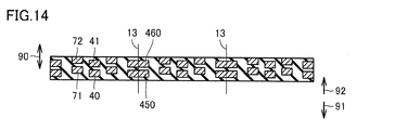
層L1,L2,L3を図13に示すように積み重ねて熱圧着させることにより、図14に示すようになる。集合補助パターン450に押されて集合ダミーパターン460は導体パターン72と同じ高さからやや第2の側92にずれる。こうして熱圧着させたものを個々の樹脂多層基板のサイズに切り分ける。
本実施の形態では、複数の樹脂多層基板を一括して製造することができるので、生産効率を上げることができる。得られる個々の樹脂多層基板は、導体パターンの外側だけでなく内側にもダミーパターンを有するので、2つのダミーパターンにより導体パターンを挟み込むことができる。これにより、積層体に含まれる異なる層に配置された導体パターン同士の間で比較したときの面方向のずれをより効果的に抑制することができる。
本実施の形態で得られる樹脂多層基板は、以下の構成を備えている。本実施の形態における樹脂多層基板は、第1ダミーパターン41と同じ高さに、前記第1材料で形成された第2ダミーパターンを備え、前記第2ダミーパターンは、第1導体パターン31および第2導体パターン32のいずれに対しても電気的に接続されておらず、第1ダミーパターン41および第2ダミーパターンは、断面図で見たときに、第1導体パターン31および第2導体パターン32のうち少なくとも一方を挟み込むように配置されている。「第2ダミーパターン」とは、たとえば、集合ダミーパターン460から切り分けられて得られるいずれかのダミーパターンのことである。図14に示す例では、ある場所では、第1ダミーパターン41と第2ダミーパターンとで第1導体パターン31を挟み込んでいる。他のある場所では、第1ダミーパターン41と第2ダミーパターンとで第2導体パターン32を挟み込んでいる。
(実施の形態6)
図15を参照して、本発明に基づく実施の形態6における樹脂多層基板の製造方法について説明する。ここでは、1つの樹脂多層基板に対応する領域に注目して示しているが、実施の形態4,5のように集合樹脂層を用いて複数の樹脂多層基板を一括して製造することとしてもよい。
図15を参照して、本発明に基づく実施の形態6における樹脂多層基板の製造方法について説明する。ここでは、1つの樹脂多層基板に対応する領域に注目して示しているが、実施の形態4,5のように集合樹脂層を用いて複数の樹脂多層基板を一括して製造することとしてもよい。
本実施の形態における樹脂多層基板の製造方法では、第1ダミーパターン41および第2ダミーパターンのうち少なくとも一方は、前記樹脂層に垂直な方向から見たときに枠状の部分を含む。ここでいう「枠状の部分」とは、完全に閉ループとなっている枠状であってもよいが、図15に層L2として示すダミーパターン48のように、1ヶ所以上の切れ目を有する枠状であってもよい。図15に示した例では、ダミーパターン48が第2ダミーパターンに相当する。ダミーパターン48は一方の辺に切れ目を有する。図15に示した例では、導体パターン71の一方の端がダミーパターン48の切れ目に入り込んでいる。図15に示したのはあくまで一例であって、この構成に限らない。たとえば導体パターン71の一方の端がダミーパターン48の切れ目を通り抜けてさらに枠の外側に延在する構成であってもよい。ダミーパターン48が2ヶ所以上の切れ目を有する構成であってもよい。層L3においては、層L2のダミーパターン48に対応する領域を占めるようにダミーパターン47が配置されている。
本実施の形態では、第1ダミーパターン41および第2ダミーパターンのうち少なくとも一方が枠状の部分を含んでいるので、導体パターン71を取り囲むようにして全周にわたって、熱圧着時の導体パターンの変位を抑制することができる。
なお、上記実施の形態のうち複数を適宜組み合わせて採用してもよい。
なお、今回開示した上記実施の形態はすべての点で例示であって制限的なものではない。本発明の範囲は請求の範囲によって示され、請求の範囲と均等の意味および範囲内でのすべての変更を含むものである。
なお、今回開示した上記実施の形態はすべての点で例示であって制限的なものではない。本発明の範囲は請求の範囲によって示され、請求の範囲と均等の意味および範囲内でのすべての変更を含むものである。
2 樹脂層、3 開口部、6 層間接続部、11,12 金型、11a,12a 凸部、13 切断線、21 第1樹脂層、22 第2樹脂層、23 第3樹脂層、31 第1導体パターン、32 第2導体パターン、33 第3導体パターン、34 第4導体パターン、40 補助パターン、41 第1ダミーパターン、41a 第1面、41b 第2面、47,48 ダミーパターン、71,72,73 導体パターン、72a,72b 外部接続電極、90 積層方向、91 第1の側、92 第2の側、101,102 樹脂多層基板、200 集合樹脂層、450 集合補助パターン、460 集合ダミーパターン。
Claims (17)
- 熱可塑性樹脂を主材料とする複数の樹脂層が積層された状態のものを含む樹脂多層基板であって、積層方向が上下方向と一致する姿勢にして前記樹脂多層基板を見たときの上側および下側のうち一方を第1の側とし、他方を第2の側としたとき、
前記樹脂多層基板は、2通り以上の高さに分散して配置され、第1材料で形成された複数の導体パターンを内部に含み、
前記複数の導体パターンのうち、前記積層方向に互いに離隔しつつ積層方向に並ぶ2つの導体パターンを、前記第1の側から順に第1導体パターンおよび第2導体パターンと呼ぶこととすると、
前記樹脂多層基板は、前記第1材料で形成された第1ダミーパターンを備え、
前記第1ダミーパターンは、前記第1の側を向く第1面と、前記第2の側を向く第2面とを有し、前記第1導体パターンおよび前記第2導体パターンのいずれに対しても電気的に接続されておらず、
前記第1導体パターンの前記第2の側の面のうち最も前記第2の側にある点よりも前記第1面の方が前記第1の側にあり、前記第2導体パターンの前記第1の側の面のうち最も前記第1の側にある点よりも前記第2面の方が前記第2の側にある、樹脂多層基板。 - 前記第1導体パターンと前記第2導体パターンとは、前記積層方向から見たときに少なくとも一部が重なる位置関係である、請求項1に記載の樹脂多層基板。
- 前記第1導体パターン、前記第2導体パターンおよび前記第1ダミーパターンが見えるような断面で前記樹脂多層基板を見たとき、
前記第1導体パターンと一体的に形成された、または、前記第1導体パターンとは別箇に形成された導体パターンが前記第1導体パターンと同じ高さに表れ、これを第3導体パターンと呼ぶこととし、
前記第2導体パターンと一体的に形成された、または、前記第2導体パターンとは別箇に形成された導体パターンが前記第2導体パターンと同じ高さに表れ、これを第4導体パターンと呼ぶこととしたとき、
前記断面において、前記第1ダミーパターンの前記第1の側の一部は、前記第1導体パターンと前記第3導体パターンとの間に挟まれており、前記第1ダミーパターンの前記第2の側の一部は、前記第2導体パターンと前記第4導体パターンとの間に挟まれている、請求項1または2に記載の樹脂多層基板。 - 前記断面における前記第1ダミーパターンの幅をW1とし、前記断面における前記第1導体パターンと前記第3導体パターンとの間の間隙の長さをW2とすると、W1≧W2/2である、請求項3に記載の樹脂多層基板。
- 前記樹脂多層基板は、前記積層方向に平行な巻回軸を有するコイル導体を含んでおり、前記第1導体パターン、前記第2導体パターン、前記第3導体パターンおよび前記第4導体パターンはいずれも前記コイル導体の一部である、請求項3または4に記載の樹脂多層基板。
- 前記樹脂多層基板は、前記積層方向に平行な巻回軸を有するコイル導体を含んでおり、前記第1導体パターンおよび前記第2導体パターンはいずれも前記コイル導体の一部である、請求項1または2に記載の樹脂多層基板。
- 前記第1ダミーパターンと同じ高さに、前記第1材料で形成された第2ダミーパターンを備え、前記第2ダミーパターンは、前記第1導体パターンおよび前記第2導体パターンのいずれに対しても電気的に接続されておらず、前記第1ダミーパターンおよび前記第2ダミーパターンは、前記第1導体パターン、前記第2導体パターン、前記第1ダミーパターンおよび前記第2ダミーパターンが見えるような断面で見たときに、前記第1導体パターンおよび前記第2導体パターンのうち少なくとも一方を挟み込むように配置されている、請求項1から6のいずれかに記載の樹脂多層基板。
- 前記第1ダミーパターンおよび前記第2ダミーパターンのうち少なくとも一方は、前記積層方向から見たときに枠状の部分を含む、請求項7に記載の樹脂多層基板。
- 前記第1材料は銅を含む、請求項1から8のいずれかに記載の樹脂多層基板。
- 請求項1から9のいずれかに記載の樹脂多層基板を得るための製造方法であって、
前記第1導体パターンを有する第1樹脂層よりも前記第2の側に、前記第2導体パターンを有する第2樹脂層を重ねる工程を含みつつ前記複数の樹脂層を積み重ねることによって積層体を得る工程と、
前記積層体を加熱および加圧することによって前記積層体を熱圧着させる工程とを含み、
前記積層体を得る工程は、前記第1樹脂層の前記第2の側の面の前記第1導体パターンが覆う領域とは別の領域に前記第1ダミーパターンが配置された状態で、前記第1樹脂層よりも前記第1の側に、前記第1ダミーパターンに対応する領域に延在する補助パターンを有する第3樹脂層を配置した状態で行なわれる、樹脂多層基板の製造方法。 - 請求項1から9のいずれかに記載の樹脂多層基板を得るための製造方法であって、
前記第1導体パターンを前記第2の側の面に有する第1樹脂層の前記第2の側に、前記第2導体パターンを前記第2の側の面に有する第2樹脂層を重ねる工程を含みつつ前記複数の樹脂層を積み重ねることによって積層体を得る工程と、
前記積層体を加熱および加圧することによって前記積層体を熱圧着させる工程とを含み、
前記積層体を得る工程は、前記第1樹脂層と前記第2樹脂層との間に第4樹脂層を配置することによって行なわれ、前記第4樹脂層は、前記第1ダミーパターンを前記第2の側の面に有する、樹脂多層基板の製造方法。 - 請求項1から9のいずれかに記載の樹脂多層基板を得るための製造方法であって、
前記第1導体パターンを有する第1樹脂層の前記第2の側に、前記第2導体パターンを有する第2樹脂層を重ねる工程を含みつつ前記複数の樹脂層を積み重ねることによって積層体を得る工程と、
前記積層体を加熱および加圧することによって前記積層体を熱圧着させる工程とを含み、
前記積層体を得る工程は、前記第1樹脂層および前記第2樹脂層のうち一方の樹脂層に前記第1ダミーパターンが配置され、他方の樹脂層には前記第1ダミーパターンに対応する領域に開口部または切欠きが設けられた状態で行なわれる、樹脂多層基板の製造方法。 - 前記熱圧着させる工程は、前記積層体の前記第1の側および前記第2の側のうち少なくとも一方に、被加圧物の凹凸に追従することができる第1部材を配置して行なわれる、請求項10から12のいずれかに記載の樹脂多層基板の製造方法。
- 前記第1部材は、クッション材を含む、請求項13に記載の樹脂多層基板の製造方法。
- 前記積層体を得る工程では、複数の樹脂多層基板に対応するサイズの集合樹脂層を用いて一括して行なうことによって集合積層体を得、
前記熱圧着する工程では、前記集合積層体を一括して加熱および加圧することによって熱圧着させ、
前記熱圧着させる工程の後に、前記集合積層体を個別の樹脂多層基板に対応するサイズに分断する工程を含む、請求項10から14のいずれかに記載の樹脂多層基板の製造方法。 - 前記分断する工程は、前記集合積層体に含まれる前記第1ダミーパターンをより大きなサイズのパターンから切り分ける工程を含む、請求項15に記載の樹脂多層基板の製造方法。
- 熱可塑性樹脂を主材料とする複数の樹脂層が積層された状態のものを含む樹脂多層基板の製造方法であって、積層方向が上下方向と一致する姿勢にして前記樹脂多層基板を見たときの上側および下側のうち一方を第1の側とし、他方を第2の側としたとき、
前記樹脂多層基板は、2通り以上の高さに分散して配置され、第1材料で形成された複数の導体パターンを内部に含み、
前記複数の導体パターンのうち、前記積層方向に互いに離隔しつつ積層方向に並ぶ2つの導体パターンを、前記第1の側から順に第1導体パターンおよび第2導体パターンと呼ぶこととすると、
前記第1導体パターンを有する第1樹脂層の前記第2の側に、前記第2導体パターンを有する第2樹脂層を重ねる工程を含みつつ前記複数の樹脂層を積み重ねることによって積層体を得る工程と、
前記積層体を加熱および加圧することによって前記積層体を熱圧着させる工程とを含み、
前記積層体を得る工程は、前記第1樹脂層および前記第2樹脂層のうち一方の樹脂層に前記第1材料で形成された第1ダミーパターンが配置され、他方の樹脂層には前記第1ダミーパターンに対応する領域に開口部または切欠きが設けられた状態で行なわれ、
前記熱圧着させる工程の後に、前記第1ダミーパターンを含む領域を切除する工程を含む、樹脂多層基板の製造方法。
Priority Applications (1)
| Application Number | Priority Date | Filing Date | Title |
|---|---|---|---|
| CN201790000419.4U CN208258201U (zh) | 2016-02-02 | 2017-01-13 | 树脂多层基板 |
Applications Claiming Priority (2)
| Application Number | Priority Date | Filing Date | Title |
|---|---|---|---|
| JP2016-018154 | 2016-02-02 | ||
| JP2016018154 | 2016-02-02 |
Publications (1)
| Publication Number | Publication Date |
|---|---|
| WO2017135014A1 true WO2017135014A1 (ja) | 2017-08-10 |
Family
ID=59499558
Family Applications (1)
| Application Number | Title | Priority Date | Filing Date |
|---|---|---|---|
| PCT/JP2017/001025 Ceased WO2017135014A1 (ja) | 2016-02-02 | 2017-01-13 | 樹脂多層基板およびその製造方法 |
Country Status (2)
| Country | Link |
|---|---|
| CN (1) | CN208258201U (ja) |
| WO (1) | WO2017135014A1 (ja) |
Citations (4)
| Publication number | Priority date | Publication date | Assignee | Title |
|---|---|---|---|---|
| JPH01137609A (ja) * | 1987-11-25 | 1989-05-30 | Matsushita Electric Ind Co Ltd | チップインダクタ |
| JP2006049502A (ja) * | 2004-08-03 | 2006-02-16 | Denso Corp | 多層基板の製造方法 |
| JP2015050422A (ja) * | 2013-09-04 | 2015-03-16 | 株式会社村田製作所 | 樹脂多層基板およびその製造方法 |
| WO2015129601A1 (ja) * | 2014-02-27 | 2015-09-03 | 株式会社村田製作所 | 電磁石の製造方法、および、電磁石 |
-
2017
- 2017-01-13 WO PCT/JP2017/001025 patent/WO2017135014A1/ja not_active Ceased
- 2017-01-13 CN CN201790000419.4U patent/CN208258201U/zh active Active
Patent Citations (4)
| Publication number | Priority date | Publication date | Assignee | Title |
|---|---|---|---|---|
| JPH01137609A (ja) * | 1987-11-25 | 1989-05-30 | Matsushita Electric Ind Co Ltd | チップインダクタ |
| JP2006049502A (ja) * | 2004-08-03 | 2006-02-16 | Denso Corp | 多層基板の製造方法 |
| JP2015050422A (ja) * | 2013-09-04 | 2015-03-16 | 株式会社村田製作所 | 樹脂多層基板およびその製造方法 |
| WO2015129601A1 (ja) * | 2014-02-27 | 2015-09-03 | 株式会社村田製作所 | 電磁石の製造方法、および、電磁石 |
Also Published As
| Publication number | Publication date |
|---|---|
| CN208258201U (zh) | 2018-12-18 |
Similar Documents
| Publication | Publication Date | Title |
|---|---|---|
| JP5652481B2 (ja) | 樹脂多層基板およびその製造方法 | |
| JP5757376B1 (ja) | 多層基板の製造方法、多層基板および電磁石 | |
| JP6424453B2 (ja) | 多層基板の製造方法および多層基板 | |
| TWI612866B (zh) | 多層基板及其製造方法 | |
| KR102123141B1 (ko) | 전자 부품 및 그 제조 방법 | |
| WO2015015975A1 (ja) | 多層基板および多層基板の製造方法 | |
| JPWO2015137226A1 (ja) | 積層コイル素子およびその製造方法 | |
| TWI537127B (zh) | 複合板結構及其製造方法 | |
| WO2017135014A1 (ja) | 樹脂多層基板およびその製造方法 | |
| JP6536751B2 (ja) | 積層コイルおよびその製造方法 | |
| JP6350758B2 (ja) | 樹脂多層基板およびその製造方法 | |
| JP4973202B2 (ja) | 多層回路基板の製造方法 | |
| JP2015050422A (ja) | 樹脂多層基板およびその製造方法 | |
| JP2014225604A (ja) | 樹脂多層基板およびその製造方法 | |
| CN208258200U (zh) | 树脂多层基板 | |
| JPWO2017010228A1 (ja) | 樹脂基板、部品搭載樹脂基板およびその製造方法 | |
| JP6729754B2 (ja) | 樹脂多層基板の製造方法 | |
| CN104144566B (zh) | 多层基板及其制造方法 | |
| WO2017159437A1 (ja) | 回路基板およびその製造方法 | |
| JP6516065B2 (ja) | 樹脂多層基板の製造方法 | |
| JP4225016B2 (ja) | 積層セラミック電子部品の製造方法および集合電子部品 | |
| WO2016039139A1 (ja) | 樹脂多層基板 | |
| JP5773105B2 (ja) | 樹脂多層基板およびその製造方法 | |
| JP2019051616A (ja) | インレットシートおよび非接触icカード | |
| JPWO2012133313A1 (ja) | 部品内蔵樹脂基板の製造方法 |
Legal Events
| Date | Code | Title | Description |
|---|---|---|---|
| 121 | Ep: the epo has been informed by wipo that ep was designated in this application |
Ref document number: 17747176 Country of ref document: EP Kind code of ref document: A1 |
|
| NENP | Non-entry into the national phase |
Ref country code: DE |
|
| 122 | Ep: pct application non-entry in european phase |
Ref document number: 17747176 Country of ref document: EP Kind code of ref document: A1 |
|
| NENP | Non-entry into the national phase |
Ref country code: JP |