WO2017115473A1 - 磁気記録媒体用ガラス基板及び磁気記録媒体 - Google Patents
磁気記録媒体用ガラス基板及び磁気記録媒体 Download PDFInfo
- Publication number
- WO2017115473A1 WO2017115473A1 PCT/JP2016/062148 JP2016062148W WO2017115473A1 WO 2017115473 A1 WO2017115473 A1 WO 2017115473A1 JP 2016062148 W JP2016062148 W JP 2016062148W WO 2017115473 A1 WO2017115473 A1 WO 2017115473A1
- Authority
- WO
- WIPO (PCT)
- Prior art keywords
- glass substrate
- outer peripheral
- magnetic recording
- peripheral end
- recording medium
- Prior art date
- Legal status (The legal status is an assumption and is not a legal conclusion. Google has not performed a legal analysis and makes no representation as to the accuracy of the status listed.)
- Ceased
Links
Images

Classifications
-
- G—PHYSICS
- G11—INFORMATION STORAGE
- G11B—INFORMATION STORAGE BASED ON RELATIVE MOVEMENT BETWEEN RECORD CARRIER AND TRANSDUCER
- G11B5/00—Recording by magnetisation or demagnetisation of a record carrier; Reproducing by magnetic means; Record carriers therefor
- G11B5/02—Recording, reproducing, or erasing methods; Read, write or erase circuits therefor
-
- G—PHYSICS
- G11—INFORMATION STORAGE
- G11B—INFORMATION STORAGE BASED ON RELATIVE MOVEMENT BETWEEN RECORD CARRIER AND TRANSDUCER
- G11B5/00—Recording by magnetisation or demagnetisation of a record carrier; Reproducing by magnetic means; Record carriers therefor
- G11B5/62—Record carriers characterised by the selection of the material
- G11B5/73—Base layers, i.e. all non-magnetic layers lying under a lowermost magnetic recording layer, e.g. including any non-magnetic layer in between a first magnetic recording layer and either an underlying substrate or a soft magnetic underlayer
- G11B5/739—Magnetic recording media substrates
- G11B5/73911—Inorganic substrates
- G11B5/73921—Glass or ceramic substrates
-
- G—PHYSICS
- G11—INFORMATION STORAGE
- G11B—INFORMATION STORAGE BASED ON RELATIVE MOVEMENT BETWEEN RECORD CARRIER AND TRANSDUCER
- G11B5/00—Recording by magnetisation or demagnetisation of a record carrier; Reproducing by magnetic means; Record carriers therefor
- G11B5/84—Processes or apparatus specially adapted for manufacturing record carriers
Definitions
- the present invention relates to a glass substrate for a magnetic recording medium and a magnetic recording medium.
- the magnetic recording apparatus includes a magnetic recording medium in which a magnetic layer or the like is formed on a magnetic recording medium substrate, and information can be recorded using the magnetic layer.
- an aluminum alloy substrate has been used as a substrate for a magnetic recording medium used in a magnetic recording apparatus.
- it is harder and more flat and smooth than an aluminum alloy substrate. Glass substrates are becoming mainstream.
- the magnetic recording density has been increased.
- the recording area per bit is miniaturized.
- the surface of the magnetic recording medium must be smooth so that the magnetic recording medium and the magnetic head do not contact each other. Is required.
- the main surface of the glass substrate for magnetic recording media which is a substrate for magnetic recording media, is also required to be extremely smooth.
- the glass substrate for a magnetic recording medium usually has a donut shape having an opening at the center, and has a pair of main surfaces, an outer peripheral end surface, and an inner peripheral end surface.
- the main surface serving as the recording surface is mirror-polished so as to be extremely smooth, and the surface roughness is sufficiently low.
- the head crash failure means that the magnetic head comes into contact with the projections on the surface of the magnetic recording medium and damages the magnetic recording medium.
- the thermal asperity failure is a phenomenon in which the magnetic head is magnetized by adiabatic compression or contact of air in a convex portion or a concave portion included in the main surface of the magnetic recording medium when the magnetic head passes while flying over the main surface of the magnetic recording medium. A failure in which a resistance effect element is heated and causes a read error.
- Patent Document 1 discloses a glass substrate for a donut type magnetic disk having a pair of main surfaces, a side wall surface, and a chamfered surface between the main surface and the side wall surface, the side wall surface and the chamfered surface.
- the surface roughness of at least one of the surfaces has an arithmetic mean roughness (Ra) of 0.015 ⁇ m or less, and a roughness cross-sectional area at a roughness percentage of 60% in the load factor curve of the roughness cross-sectional area.
- Ra arithmetic mean roughness
- a magnetic disk glass substrate is disclosed in which the load factor is 95% or more.
- an object of one aspect of the present invention is to provide a glass substrate for a magnetic recording medium that can suppress adhesion of foreign matters to the main surface due to minute wrinkles on the outer peripheral end surface. To do.
- the present invention relates to the following ⁇ 1> to ⁇ 8>.
- a glass substrate for a magnetic recording medium having a donut shape and having a pair of main surfaces, an outer peripheral end surface, and an inner peripheral end surface, The outer peripheral end surface has an outer peripheral side surface portion and a pair of outer peripheral chamfered portions, A glass substrate for a magnetic recording medium, wherein a ratio of an area occupied by a concave defect in the outer peripheral end face is 0.05% or less.
- ⁇ 2> The glass substrate for a magnetic recording medium according to ⁇ 1>, wherein a ratio of an area occupied by the concave defect in the outer peripheral end face is 0.01% or less.
- ⁇ 3> The glass substrate for a magnetic recording medium according to ⁇ 1>, wherein a ratio of an area occupied by the concave defect in the outer peripheral end face is 0.005% or less.
- the ratio of the area of the area occupied by the concave defect in the outer peripheral end surface is: For the outer peripheral end surface, obtain a surface image, In the surface image, a threshold value is provided so that the brightness of the concave defect included in the outer peripheral side surface part and the pair of outer peripheral chamfered parts can be separated from the brightness of the part other than the concave defect, Forming a binarized surface image obtained by binarizing the surface image with the threshold value; The glass substrate for magnetic recording media according to any one of ⁇ 1> to ⁇ 3>, calculated from the binarized surface image.
- ⁇ 5> The magnetic according to any one of ⁇ 1> to ⁇ 4>, wherein a maximum defect area which is an area of a concave defect having the largest area among the concave defects of the outer peripheral end surface is 1000 ⁇ m 2 or less.
- ⁇ 6> The glass substrate for a magnetic recording medium according to ⁇ 5>, wherein the maximum defect area is 100 ⁇ m 2 or less.
- ⁇ 7> The glass substrate for magnetic recording media according to any one of ⁇ 1> to ⁇ 6>, which is a glass substrate for magnetic recording media for energy-assisted magnetic recording media.
- a magnetic recording medium comprising the glass substrate for a magnetic recording medium according to any one of ⁇ 1> to ⁇ 7>.
- the glass substrate for a magnetic recording medium of the present invention it is possible to provide a glass substrate for a magnetic recording medium that can suppress adhesion of foreign matters to the main surface due to minute wrinkles on the outer peripheral end surface.
- FIG. 1 is an explanatory view schematically showing a perspective sectional view of a glass substrate for a magnetic recording medium.
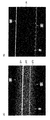
- 2A is an explanatory diagram of a surface image of the outer peripheral end surface of the magnetic recording medium glass substrate
- FIG. 2B is a binarized surface image of the outer peripheral end surface of the magnetic recording medium glass substrate. It is explanatory drawing.
- the glass substrate for a magnetic recording medium of the present embodiment is a glass substrate for a magnetic recording medium having a donut shape and having a pair of main surfaces, an outer peripheral end surface, and an inner peripheral end surface, and the outer peripheral end surface is an outer peripheral side surface. And a pair of outer peripheral chamfers.
- the ratio of the area of the area occupied by the concave defects in the outer peripheral end face can be 0.05% or less.
- glass substrate for a magnetic recording medium of the present embodiment (hereinafter also simply referred to as “glass substrate”) will be described with reference to FIG.
- FIG. 1 schematically shows a perspective sectional view of the glass substrate of the present embodiment.
- FIG. 1 is a perspective cross-sectional view including a cross section in a plane that passes through the center of the glass substrate 10 for a magnetic recording medium and is perpendicular to the main surfaces 121 and 122. That is, in FIG. 1, the half of the glass substrate of this embodiment and sectional drawing are shown collectively.
- the glass substrate 10 has a circular shape on the outer periphery, and a circular shape in which a circular opening (center opening) 11 is provided in the center so as to be concentric with the outer periphery, that is, a donut. It has a shape.
- the upper and lower surfaces are main surfaces 121 and 122.
- the glass substrate 10 has the outer peripheral end surface 13 located in an outer periphery, and the inner peripheral end surface 14 located in an inner periphery.
- the outer peripheral end surface 13 and the inner peripheral end surface 14 can have chamfered portions on the main surfaces 121 and 122 side, respectively. That is, the outer peripheral end surface 13 and the inner peripheral end surface 14 can each have a pair of chamfered portions. Specifically, the outer peripheral end surface 13 can have outer peripheral chamfered portions 131 and 133, and the inner peripheral end surface 14 can have inner peripheral chamfered portions 141 and 143, respectively.
- a side surface portion can be formed between the chamfered portions, the outer peripheral end surface 13 can have the outer peripheral side surface portion 132, and the inner peripheral end surface 14 can have the inner peripheral side surface portion 142.
- the outer peripheral side surface portion 132 and the inner peripheral side surface portion 142 can be formed so as to be substantially perpendicular to the main surfaces 121 and 122, respectively.
- the outer peripheral end surface 13 can include the outer peripheral side surface portion 132 and the outer peripheral chamfered portions 131 and 133
- the inner peripheral end surface 14 can include the inner peripheral side surface portion 142 and the inner peripheral chamfered portions 141 and 143.
- the size of the glass substrate 10 of this embodiment is not specifically limited, It can select arbitrarily according to the specification of a glass substrate.
- the diameter D of the glass substrate of this embodiment can be made into the size according to the specification requested
- the diameter of the glass substrate of the present embodiment is preferably 65 mm or more, for which demand has been increasing in recent years.
- polishing grains or the like may have entered the wrinkle in the manufacturing process.
- the glass substrate processed so as to have a predetermined shape and surface property is subjected to a step of forming a magnetic layer or the like to form a magnetic recording medium.
- the abrasive grains that have entered the cage In some cases, foreign substances such as those move and adhere to the main surface side.
- Arithmetic mean roughness only evaluates an extremely narrow area of, for example, an arbitrary 50 ⁇ m square in the outer peripheral end face, and does not evaluate the entire outer peripheral end face. And the surface property of the outer peripheral end face is not completely uniform. For this reason, even when the arithmetic average roughness of the outer peripheral end face is within a predetermined range, if fine wrinkles are included outside the evaluation area, the main surface is caused by the fine wrinkles outside the evaluation area. The inventor of the present invention has found that the adhesion of foreign matter has occurred.
- the inventor of the present invention has further intensively studied a glass substrate that can suppress adhesion of foreign matters to the main surface due to minute wrinkles on the outer peripheral end face.
- the ratio of the area of the area occupied by the concave defects, which are minute wrinkles contained on the surface of the outer peripheral end face, is a glass substrate of 0.05% or less, which is mainly caused by the fine wrinkles on the outer peripheral end face.
- the present inventors have found that the adhesion of foreign matter to the surface can be suppressed and completed the present invention.
- the ratio of the area occupied by the concave defects in the outer peripheral end surface is preferably 0.05% or less, more preferably 0.01% or less, and 0.005% or less as described above. More preferably.
- the ratio of the area occupied by the concave defects in the outer peripheral end surface calculated from the binarized surface image by an evaluation method described later is evaluated, and a glass substrate of 0.05% or less is manufactured. By doing so, it is possible to suppress adhesion of foreign matter to the main surface due to minute wrinkles contained in the outer peripheral end face.
- the lower limit value is not limited, and may be, for example, larger than 0%.
- a surface image of the entire peripheral surface is acquired along the outer periphery of the outer peripheral end surface (surface image acquisition step).
- An example of the acquired surface image is shown in FIG.
- the surface image of the entire peripheral surface of the outer peripheral end surface is between the upper end portion 21A on the main surface side and the lower end portion 21B on the main surface side opposite to the main surface.
- the outer peripheral chamfered portions 221 and 223 and the outer peripheral side surface portion 222 are included.
- the concave defect 23 is formed in a dotted line shape on the outer peripheral chamfered portion 223 on the lower end portion 21B side.
- the means for acquiring the surface image for the outer peripheral end face is not particularly limited, and various imaging means can be used. However, it is preferable to use an imaging means provided with resolution and / or optical image enlargement means so that a concave defect formed on the outer peripheral end surface of the glass substrate can be detected.
- the glass substrate When acquiring the surface image of the entire peripheral surface of the outer peripheral end surface in the surface image acquisition step, the glass substrate has a disk shape, and thus, for example, the surface image of the glass substrate is captured and acquired at a plurality of measurement points. Can do.
- a threshold value is set so that the brightness of the concave defect included in the outer peripheral side surface portion and the pair of outer peripheral chamfered portions in the acquired surface image can be separated from the brightness of the portion other than the concave defect (threshold setting step).
- the brightness distribution region in the surface image is different between the concave defect in the outer peripheral end face and the portion other than the concave defect. This is presumably because the concave defect portion has a different surface state from the other portions. Therefore, by specifying a lightness distribution region including a concave defect and performing binarization processing described later, both can be identified.
- the lightness distribution region including the concave defect is continuous, and the lightness distribution region other than the concave defect is located in a region where the lightness is smaller or larger than the lightness distribution region including the concave defect. Yes.
- the threshold value setting step it is possible to set two threshold values, that is, an upper limit value and a lower limit value of the brightness area including the concave defects while comparing the surface image and the brightness distribution of the surface image.
- a binarized surface image can be formed by binarizing the surface image with the threshold value (binarized surface image forming step).
- FIG. 2B corresponds to a binarized surface image obtained by binarizing the surface image shown in FIG.
- the brightness area between the upper limit value and the lower limit value of the brightness distribution area including the concave defect, which is the threshold set in the threshold setting step, is white, and the other brightness distribution areas Is binarizing black.
- the concave defect 23 is white between the upper end 21A and the lower end 21B on the main surface side of the outer peripheral end surface, and the other portion 24 is black. ing. For this reason, it was confirmed that the concave defect 23 and the other portion 24 in the outer peripheral end face could be identified by setting the brightness threshold.
- the area of the concave defect 23 that is, the area of the brightness area sandwiched between the two set threshold values and the area of the outer peripheral end face are calculated, and the concave defect in the outer peripheral end face is calculated.
- the area ratio of the occupied area can be calculated.
- the glass substrate of the present embodiment has an area of the concave defect having the largest area among the concave defects of the outer peripheral end surface, and the maximum defect area is preferably 1000 ⁇ m 2 or less, and is 100 ⁇ m 2 or less. Is more preferable.
- the maximum defect area is 1000 ⁇ m 2 or less, it is difficult for foreign matters such as abrasive grains to enter, and the main surface is caused by minute wrinkles contained in the outer peripheral end face. In particular, the adhesion of foreign matter can be suppressed.
- the maximum defect area can be calculated, for example, by calculating the area of each concave defect from the above-mentioned binarized surface image and selecting the area of the maximum concave defect.
- the lower limit value is not limited and can be said to be, for example, larger than 0 ⁇ m 2 .
- the area of the concave defect, which is a fine flaw, occupying the entire area of the outer peripheral end face can be 0.05% or less. That is, the ratio of the concave defects included in the entire outer peripheral end face can be sufficiently reduced. For this reason, the adhesion of foreign matter to the main surface due to minute wrinkles contained in the outer peripheral end face can be suppressed.
- the magnetic recording medium produced using the glass substrate for magnetic recording medium has problems such as head crash failure and thermal asperity failure. It can be suppressed.
- a magnetic recording medium using an energy-assisted magnetic recording method that has been attracting attention in recent years that is, an energy-assisted magnetic recording medium
- the glass substrate of the present embodiment it is possible to suppress the adhesion of foreign matters to the main surface of the glass substrate as described above. The occurrence of defects can be suppressed.
- the glass substrate of the present embodiment can be particularly suitably used as a glass substrate for a magnetic recording medium for an energy-assisted magnetic recording medium.
- minute wrinkles on the outer peripheral end face can be sufficiently suppressed.
- minute wrinkles on the outer peripheral end face can be suppressed, crack extension and crack generation due to rapid heating and rapid cooling during film formation can be suppressed.
- an ordered alloy having a large magnetic anisotropy coefficient Ku is used as the magnetic material of the magnetic layer, so that a high Ku can be realized by increasing the degree of ordering (regularity).
- a base material including a glass substrate for a magnetic recording medium is heat-treated when the magnetic layer is formed. For this reason, it may be rapidly heated and rapidly cooled during the production process, and according to the conventional glass substrate, the glass substrate may be cracked during the production.
- the glass substrate of the present embodiment the extension of cracks and the occurrence of cracks can be suppressed even when rapid heating or rapid cooling is applied as described above. For this reason, the glass substrate of this embodiment can be suitably used as a glass substrate for a magnetic recording medium for an energy-assisted magnetic recording medium even from this viewpoint.
- the use of the glass substrate of the present embodiment is not limited to a glass substrate for energy-assisted magnetic recording media, and can be suitably used as a glass substrate for various magnetic recording media.
- glass substrate manufacturing method a configuration example of the glass substrate for a magnetic recording medium according to the present embodiment described so far (hereinafter simply referred to as “glass substrate manufacturing method”) will be briefly described.
- the glass substrate for magnetic recording media as stated above can be manufactured.
- some description is abbreviate
- the glass substrate manufacturing method of the present embodiment can include, for example, the following steps 1 to 5.
- Step 1 A shape imparting step in which a glass substrate is processed into a disk-shaped glass substrate having a circular hole in the center.
- Step 2 A chamfering step for chamfering the end surfaces (inner and outer end surfaces) of the inner and outer periphery of the glass substrate.
- Step 3 An end surface polishing step for polishing the end surfaces (the inner peripheral end surface and the outer peripheral end surface) of the glass substrate.
- Step 4) A main surface polishing step for polishing the main surface of the glass substrate.
- Step 5 A cleaning / drying step of cleaning and drying the glass substrate.
- the shape imparting step of (Step 1) includes a glass-shaped substrate formed by a float method, a fusion method, a press forming method, a down draw method or a redraw method, and a disk-shaped glass having a circular hole in the center.
- the substrate is processed.
- the glass substrate used may be amorphous glass, crystallized glass, or tempered glass having a tempered layer on the surface of the glass substrate.
- the inner peripheral end surface and the outer peripheral end surface can be chamfered.
- the inner peripheral chamfered portions 141 and 143 can be formed on the inner peripheral end surface 14, and the outer peripheral chamfered portions 131 and 133 can be formed on the outer peripheral end surface 13.
- the end surface (side surface portion and chamfered portion) of the glass substrate can be subjected to end surface polishing.
- the polishing liquid is supplied to both the pair of main surfaces of the glass substrate having a donut shape by, for example, a double-side polishing apparatus, and the upper and lower main surfaces of the glass substrate having a donut shape are simultaneously polished. it can.
- the main surface polishing step may be only the primary main surface polishing step, the primary main surface polishing step and the secondary main surface polishing step may be performed, or the tertiary main surface polishing step may be performed after the secondary main surface polishing step. Good.
- wrapping of the main surface may be performed before performing the primary main surface polishing of the main surface.
- wrapping of the main surface for example, free abrasive wrap, fixed abrasive wrap, etc.
- wrapping of the main surface may be performed before performing the primary main surface polishing of the main surface.
- only the primary main surface lapping process may be performed, and a plurality of lapping processes such as a secondary main surface lapping process may be performed.
- glass substrate cleaning inter-process cleaning
- glass substrate surface etching inter-process etching
- main surface lapping is a broad surface main surface polishing.
- the cleaning / drying step of (Step 5) is a step of cleaning and drying the polished glass substrate.
- a specific cleaning method is not particularly limited. For example, cleaning can be performed by scrub cleaning using a detergent, ultrasonic cleaning in a state immersed in a detergent solution, ultrasonic cleaning in a state immersed in pure water, or the like. Moreover, it does not specifically limit about the drying method, For example, it can dry with isopropyl alcohol vapor
- the glass substrate may be cleaned (inter-process cleaning) or the glass substrate surface may be etched (inter-process etching) between the steps (step 1) to (step 5).
- a strengthening step for example, a chemical strengthening step for forming a reinforcing layer on the surface layer of the glass substrate before the polishing step mentioned in (Step 3) or (Step 4), Or you may implement after a grinding
- Steps 1 to (Step 5) described so far need not be performed in the order described, and for example, a main surface polishing step may be performed before the shape imparting step. Further, each step is not limited to one time, and can be performed any number of times according to the required glass substrate specifications.
- the glass substrate described above can be manufactured by the glass substrate manufacturing method of the present embodiment. For this reason, it is preferable to select the order of the processes and conditions so that minute wrinkles on the outer peripheral end face can be sufficiently reduced and removed.
- a glass substrate for polishing the main surface can be disposed in the hole provided in the carrier, and polishing can be performed by a double-side polishing apparatus. For this reason, depending on the length of polishing time in the main surface polishing step, the carrier and the outer peripheral end surface of the glass substrate may rub against each other, and fine wrinkles may be generated on the outer peripheral end surface of the glass substrate. For this reason, it is preferable to perform an end surface polishing process (process 3) after the main surface polishing process with a large polishing amount.
- a primary end surface polishing step, a primary main surface polishing step, a secondary end surface polishing step, a secondary main surface polishing step It is preferable to perform (Step 3) and (Step 4) alternately in this order.
- the said process shows the example of the order of a main surface grinding
- the timing which implements another process is not limited.
- the above-described shape imparting step, chamfering step, and the like can be performed before the primary end surface polishing step.
- it can also have a primary main surface lapping process of lapping the main surface before the primary main surface polishing process.
- cleaning / drying process, etc. can also be implemented each time.
- both the primary end surface polishing step and the secondary end surface polishing step can be performed under the same conditions.
- a glass substrate laminate is formed by laminating glass substrates.
- a substantially cylindrical (roll-shaped) brush is disposed so as to be substantially parallel to the central axis of the glass substrate laminate, and so that the outer peripheral end surface of the glass substrate laminate and the brush are in contact with each other.
- a separate substantially cylindrical brush for polishing the inner peripheral end face is separately provided so as to be substantially parallel to the central axis of the glass substrate laminate and the inner circumference of the glass substrate laminate. Arrange so that the end face and brush are in contact.
- the glass substrate laminate and the brush are in contact with each other as described above, the glass substrate laminate and / or the brush are rotated while supplying the polishing liquid between the glass substrate laminate and the brush. By doing so, it is possible to polish the end face of the glass substrate.
- polishing can be performed by changing the conditions between the primary end face polishing step and the secondary end face polishing step.
- the end face polishing is performed using a polishing pad having a softer surface, specifically, for example, a substantially cylindrical polishing pad in which a non-woven fabric is arranged on the surface that is the polishing face, instead of the brush. You can also.
- end face polishing is performed using a polishing pad in which a nonwoven fabric is disposed on the polishing surface in this way, it is preferable because minute wrinkles on the end face, particularly the outer peripheral end face, can be reduced.
- a (tertiary) end surface polishing process can be further performed after the final main surface polishing process, that is, the secondary main surface polishing process.
- the (tertiary) end surface polishing step is performed after the last main surface polishing step, the glass substrate is not made into a laminate so as not to wrinkle the main surface, one by one, that is, in a single wafer. It is preferable to perform an end surface polishing step.
- polishing pad for example, a polishing pad having a softer surface, specifically, a polishing pad in which a nonwoven fabric is disposed on the polishing surface, a suede polishing pad, or the like can be preferably used instead of the brush. .
- the secondary end surface polishing step may be performed as the secondary end surface polishing step after the secondary main surface polishing step without performing the secondary end surface polishing step after the primary main surface polishing step.
- the glass substrate for a magnetic recording medium described above can be manufactured.
- the glass substrate for magnetic recording media which can suppress adhesion of the foreign material to the main surface resulting from the fine wrinkles of an outer peripheral end surface can be manufactured.
- Magnetic recording medium Next, a configuration example of the magnetic recording medium of this embodiment will be described.
- the magnetic recording medium of the present embodiment can include the above-described glass substrate for a magnetic recording medium.
- the configuration of the magnetic recording medium of the present embodiment is not limited as long as it includes the glass substrate for magnetic recording medium described above.
- a magnetic layer is formed on the surface of the glass substrate for magnetic recording medium.
- a protective layer is formed on the surface of the glass substrate for magnetic recording medium.
- a protective layer is formed on the surface of the glass substrate for magnetic recording medium.
- a protective layer is formed on the surface of the glass substrate for magnetic recording medium.
- a protective layer is formed on the surface of the glass substrate for magnetic recording medium.
- a lubricating layer is formed on the surface of the glass substrate for magnetic recording medium.
- the magnetic recording medium includes a horizontal magnetic recording method and a vertical magnetic recording method.
- a specific manufacturing method will be described below by taking the perpendicular magnetic recording method as an example.
- the magnetic recording medium can have a magnetic layer, a protective layer, and a lubricating layer on the surface of the glass substrate for a magnetic recording medium as described above.
- a soft magnetic underlayer made of a soft magnetic material that plays a role of circulating a recording magnetic field from a magnetic head is generally provided.
- a soft magnetic underlayer, a nonmagnetic intermediate layer, a perpendicular recording magnetic layer, a protective layer, and a lubricating layer can be stacked in this order from the surface of the magnetic recording medium glass substrate.
- soft magnetic underlayer for example, CoNiFe, FeCoB, CoCuFe, NiFe, FeAlSi, FeTaN, FeN, FeTaC, CoFeB, CoZrN, etc. can be used.
- the nonmagnetic intermediate layer is made of Ru, Ru alloy or the like. This nonmagnetic intermediate layer has a function for facilitating the epitaxial growth of the perpendicular recording magnetic layer and a function for breaking the magnetic exchange coupling between the soft magnetic underlayer and the perpendicular recording magnetic layer.
- the perpendicular recording magnetic layer is a magnetic film having an easy axis of magnetization oriented in a direction perpendicular to the substrate surface, and can contain at least Co and Pt.
- a well-isolated fine particle structure (granular structure) is preferable. Specifically, an oxide (SiO 2 , SiO, Cr 2 O 3 , CoO, Ta 2 O 3 , TiO 2, etc.), Cr, B, Cu, Ta, Zr or the like added to a CoPt alloy or the like Should be used.
- the soft magnetic underlayer, nonmagnetic intermediate layer, and perpendicular recording magnetic layer described so far can be continuously manufactured by an in-line sputtering method, a DC magnetron sputtering method, or the like.
- the protective layer is provided to prevent corrosion of the perpendicular recording magnetic layer and to prevent damage to the surface of the medium even when the magnetic head comes into contact with the medium, and is provided on the perpendicular recording magnetic layer.
- a material containing C, ZrO 2 , SiO 2 or the like can be used as the protective layer.
- an in-line sputtering method for example, an in-line sputtering method, a CVD method, a spin coating method, or the like can be used.
- a lubricating layer is formed on the surface of the protective layer in order to reduce friction between the magnetic head and the recording medium (magnetic disk).
- the lubricating layer for example, perfluoropolyether, fluorinated alcohol, fluorinated carboxylic acid, or the like can be used.
- the lubricating layer can be formed by a dip method, a spray method, or the like.
- the magnetic recording medium of the present embodiment described above includes the above-described glass substrate for magnetic recording medium. That is, it includes a glass substrate for a magnetic recording medium that can suppress adhesion of foreign matter to the main surface due to minute wrinkles on the outer peripheral end face. For this reason, the magnetic recording medium of the present embodiment can suppress the occurrence of problems such as head crash failure and thermal asperity failure.
- the observation field of view can be sufficiently widened while being sufficiently enlarged to detect the concave defect, and the local observation It will not be. For this reason, it is easy to detect the concave defect, and the possibility of overlooking the existence of the concave defect can be sufficiently suppressed.
- the interval between the measurement points is selected according to the field of view of the microscope so that the entire outer peripheral end surface can be measured along the peripheral surface, one measurement point, the center of the glass substrate, and one measurement point. And the other measurement points adjacent to each other were selected so that the angle formed was 30 °. And the surface image of the whole peripheral surface of the outer peripheral end surface of a glass substrate was acquired.
- a threshold value was provided so that the brightness of the concave defect included in the outer peripheral side surface portion and the pair of outer peripheral chamfer portions and the brightness of the other portions in the acquired surface image could be separated. Specifically, while comparing the acquired surface image with the brightness distribution of the surface image, two threshold values, an upper limit value and a lower limit value, of the brightness area including the concave defect were set.
- a binarized surface image was formed by binarizing the surface image using the threshold set in the threshold setting step.
- the maximum defect area of the concave defect The area of each concave defect is calculated from the binarized surface image formed when calculating the area ratio of the area occupied by the concave defect in the outer peripheral end surface, and the most area The area of the concave defect having a large is defined as the maximum defect area.
- the amount of particles adhering to the main surface of the glass substrate produced in each experimental example is measured using a light scattering surface observing device (manufactured by KLA Tencor, Inc .: OSA Candela 6300). The amount of particles measured at this time is used as a count before cleaning.
- the glass substrate is put in a water tank containing ultrapure water, and the glass substrate is immersed in the water tank for 2 minutes in a state where ultrasonic waves of 38 kHz are applied to the water tank.
- the glass substrate is taken out from the water tank and dried by spin drying (manufactured by Semitool).
- particle increase rate is calculated by the following equation.
- (Particle increase rate:%) [(Count after cleaning) ⁇ (Count before cleaning)] / (Count after cleaning) ⁇ 100
- the obtained particle increase rate is evaluated as ⁇ when it is 0% or more and 100% or less, evaluated as ⁇ when it is larger than 100% and 260% or less, and ⁇ when it exceeds 260%. And evaluate.
- the magnetic recording medium is acceptable because it can sufficiently suppress the occurrence of problems such as head crash failure and thermal asperity failure.
- problems such as head crash failure and thermal asperity failure may occur, resulting in failure.
- Experimental examples 1 to 5 are examples, and experimental examples 6 to 8 are comparative examples.
- Experimental examples 1 to 5 are examples, and experimental examples 6 to 8 are comparative examples.
- Each step is performed in the following order to produce a glass substrate for a magnetic recording medium.
- Shape In order to obtain a glass substrate for a magnetic recording medium having an outer diameter of 65 mm, an inner diameter of 20 mm, and a plate thickness of 0.8 mm, a glass substrate formed by a float method is used as a glass substrate having a donut shape having a circular hole in the center. Process.
- the inner diameter means the diameter of the central opening.
- End face polishing process Primary end face polishing process
- a glass substrate that has been subjected to the chamfering process under similar conditions is laminated through a resin spacer to form a glass substrate laminate.
- two substantially cylindrical nylon brushes as a polishing tool, the side surface of the brush and the glass substrate constituting the glass substrate laminate, respectively, with respect to the inner peripheral end face and outer peripheral end face of the glass substrate laminate Press to make contact with the end face.
- a cerium oxide abrasive having an average particle size of 1 ⁇ m or less is supplied between the glass substrate laminate and the brush in a state where the end surface of the glass substrate of the glass substrate laminate and the side surface of the brush are in contact with each other. While rotating the glass substrate laminate and the brush. Thereby, the inner peripheral end face and the outer peripheral end face are polished.
- the average particle size means the particle size at an integrated value of 50% in the particle size distribution obtained by the laser diffraction / scattering method. In other parts of the specification, average particle size has a similar meaning.
- the polishing time is 90 minutes, and the polishing amount is 55 ⁇ m.
- the glass substrate After completion of the main surface polishing process (primary lapping process), the glass substrate is washed to remove grinding fluid and other contaminants.
- Main surface polishing step Primary main surface polishing step
- a double-side polishing apparatus manufactured by Hamai Sangyo Co., Ltd., product name: 16BF Polish the main surface.
- the removal amount by polishing is 20 ⁇ m.
- End face polishing process Secondary end face polishing process
- a glass substrate that has been subjected to the same conditions up to the main surface polishing step (primary main surface polishing step) is laminated through a resin spacer to form a glass substrate laminate.
- two polishing pads each having a substantially cylindrical shape, in which a nonwoven fabric is disposed on the polishing surface as a polishing tool are used as the polishing surface of the polishing pad with respect to the inner peripheral end surface and the outer peripheral end surface of the glass substrate laminate.
- an end face of the glass substrate constituting the glass substrate laminate are pressed against each other.
- a cerium oxide abrasive having an average particle size of 1 ⁇ m or less is placed between the glass substrate laminate and the polishing pad in a state where the end surface of the glass substrate of the glass substrate laminate and the side surface of the polishing pad are in contact with each other. While supplying, the glass substrate laminate and the polishing pad are rotated. Thereby, the inner peripheral end face and the outer peripheral end face are polished. At this time, the polishing time is 10 minutes, and the polishing amount is 20 ⁇ m.
- Main surface polishing step Secondary main surface polishing step
- a suede type polyurethane polishing pad and a polishing liquid containing colloidal silica having an average particle diameter of 20 nm as a polishing tool
- a double-side polishing apparatus manufactured by Hamai Sangyo Co., Ltd., product name: 16BF Polish the main surface.
- the removal amount by polishing is 2 ⁇ m.
- End polishing process Tertiary end polishing process
- a suede type polyurethane polishing pad as a polishing tool and a grinding liquid containing colloidal silica having an average particle diameter of 20 nm
- the outer peripheral end face is polished for each glass substrate, that is, for 5 minutes with a single wafer.
- the glass substrate that has undergone the end surface polishing process (tertiary end surface polishing step) is sequentially subjected to scrub cleaning, ultrasonic cleaning in a state of being immersed in a detergent solution, and ultrasonic cleaning in a state of being immersed in pure water (precision cleaning). Dry with isopropyl alcohol vapor.
- the glass substrate for a magnetic recording medium obtained by the above procedure is evaluated for the ratio of the area occupied by the concave defects in the outer peripheral end face described above, the maximum defect area of the concave defects, and the particle increase rate. The results are shown in Table 1.
- Table 2 summarizes the polishing time in the end face polishing step.
- the maximum defect area is 1000 ⁇ m 2 or less, and it can be confirmed that the size of the individual concave defects included in the outer peripheral end surface is small.
Landscapes
- Chemical & Material Sciences (AREA)
- Engineering & Computer Science (AREA)
- Ceramic Engineering (AREA)
- Inorganic Chemistry (AREA)
- Magnetic Record Carriers (AREA)
- Manufacturing Of Magnetic Record Carriers (AREA)
- Recording Or Reproducing By Magnetic Means (AREA)
Abstract
本発明は、外周端面の微小な疵に起因した、主表面への異物の付着を抑制できる磁気記録媒体用ガラス基板を提供することを目的とする。本発明は、ドーナツ形状を有し、一対の主表面と、外周端面と、内周端面と、を有する磁気記録媒体用ガラス基板であって、前記外周端面は外周側面部と一対の外周面取り部とを有し、前記外周端面中の、凹状欠点が占める領域の面積の割合が0.05%以下である磁気記録媒体用ガラス基板に関する。
Description
本発明は、磁気記録媒体用ガラス基板及び磁気記録媒体に関する。
磁気記録装置は、磁気記録媒体用基板上に磁性層等を成膜した磁気記録媒体を備えており、該磁性層を用いて情報を記録することができる。
磁気記録装置に用いられる磁気記録媒体用基板としては、従来、アルミニウム合金基板が使用されてきたが、高記録密度化の要求に伴い、アルミニウム合金基板に比べて硬く、平坦性や平滑性に優れるガラス基板が主流となってきている。
近年では、年々高まる高記録密度化のニーズに応えるため、磁気記録の高記録密度化が図られている。例えば垂直磁気記録方式等を採用することで、1ビット当たりの記録領域の微細化が図られている。
そして、磁気記録媒体上での1ビット当たりの記録領域の微細化に伴い、磁気記録媒体からの信号は微弱になってきている。微弱な信号の読み取り及び記録のため、磁気記録媒体と磁気ヘッドとの距離をできるだけ接近させる要求が出てきている。
回転する磁気記録媒体と磁気ヘッドとの間の距離、すなわち磁気ヘッドの浮上量を小さくするためには、磁気記録媒体と磁気ヘッドとが接触しないように、磁気記録媒体の表面が平滑であることが求められる。このため、磁気記録媒体の基板である磁気記録媒体用ガラス基板の主表面についても、極めて平滑にすることが求められる。
磁気記録媒体用ガラス基板は、通常、中央に開口部を有するドーナツ形状を有し、一対の主表面と、外周端面と、内周端面と、を有している。そして、記録面となる主表面については、極めて平滑になるように、鏡面研磨が施され、表面粗さが十分に低くなっている。
しかし、主表面の表面粗さを十分に小さくした場合でも、ヘッドクラッシュ障害やサーマルアスペリティ障害等の不具合を生じる場合があった。
なお、ヘッドクラッシュ障害とは、磁気ヘッドが磁気記録媒体表面の凸部等と接触し、磁気記録媒体等を損傷することをいう。また、サーマルアスペリティ障害とは、磁気記録媒体の主表面上を磁気ヘッドが浮上飛行しながら通過する際、磁気記録媒体の主表面に含まれる凸部または凹部において、空気の断熱圧縮または接触により磁気抵抗効果型素子が加熱され、読み出しエラーを生じる障害をいう。
係る不具合の主な原因については、従来から検討がなされており、原因の1つとして、主表面に付着した研磨砥粒等の異物が挙げられている。
磁気記録媒体用ガラス基板を製造する際には、主表面の研磨工程や、端面(外周端面及び/又は内周端面)の研磨工程を行った後、洗浄、乾燥を行っている。このため、研磨工程で用いた研磨砥粒は除去されているが、端面、特に外周端面に微小な疵があると、該疵内に研磨砥粒等が入り込み、洗浄工程で十分に除去できない場合がある。そして、外周端面の微小な疵に研磨砥粒等が入り込んだ磁気記録媒体用ガラス基板を、磁性層等を成膜する前工程で洗浄する際や、磁性層の成膜工程等を実施する場所へ搬送する際に、該研磨砥粒が主表面に移動、付着する場合があった。
このため、端面部分について所定の算術平均粗さとして、外周端面に研磨砥粒等が入り込まないようにすることが提案されていた。
例えば特許文献1には、一対の主表面と、側壁面と、主表面と側壁面との間の面取面とを有するドーナツ型の磁気ディスク用ガラス基板であって、側壁面及び面取面の少なくともいずれか一方の面の表面性状に関し、算術平均粗さ(Ra)が0.015μm以下であって、かつ粗さ断面積の負荷率曲線において、粗さ百分率が60%における粗さ断面積の負荷率は95%以上であることを特徴とする、磁気ディスク用ガラス基板が開示されている。
しかしながら、特許文献1に開示された磁気ディスク用ガラス基板を用いたとしても、外周端面の微小な疵に起因したと考えられる、主表面への異物の付着を十分には抑制できていなかった。このような外周端面の微小な傷は、例えば主表面研磨工程等において研磨キャリア等との接触で、ランダムに発生することがある。
そこで、本発明の一側面では上記従来技術が有する課題に鑑み、外周端面の微小な疵に起因した、主表面への異物の付着を抑制できる磁気記録媒体用ガラス基板を提供することを目的とする。
すなわち、本発明は下記<1>~<8>に関するものである。
<1> ドーナツ形状を有し、一対の主表面と、外周端面と、内周端面と、を有する磁気記録媒体用ガラス基板であって、
前記外周端面は外周側面部と一対の外周面取り部とを有し、
前記外周端面中の、凹状欠点が占める領域の面積の割合が0.05%以下である磁気記録媒体用ガラス基板。
<2> 前記外周端面中の、前記凹状欠点が占める領域の面積の割合が0.01%以下である前記<1>に記載の磁気記録媒体用ガラス基板。
<3> 前記外周端面中の、前記凹状欠点が占める領域の面積の割合が0.005%以下である前記<1>に記載の磁気記録媒体用ガラス基板。
<4> 前記外周端面中の、前記凹状欠点が占める領域の面積の割合は、
前記外周端面について、表面画像を得て、
前記表面画像中の、前記外周側面部、及び一対の前記外周面取り部に含まれる凹状欠点の明度と、前記凹状欠点以外の部分の明度とが分離できるように閾値を設け、
前記表面画像を前記閾値で二値化した、二値化処理済み表面画像を形成し、
前記二値化処理済み表面画像から算出する、前記<1>乃至<3>のいずれか一に記載の磁気記録媒体用ガラス基板。
<5> 前記外周端面が有する前記凹状欠点のうち、最も面積の大きい凹状欠点の面積である最大欠点面積が1000μm2以下である、前記<1>乃至<4>のいずれか一に記載の磁気記録媒体用ガラス基板。
<6> 前記最大欠点面積が100μm2以下である前記<5>に記載の磁気記録媒体用ガラス基板。
<7> エネルギーアシスト磁気記録媒体用の磁気記録媒体用ガラス基板である、前記<1>乃至<6>のいずれか一に記載の磁気記録媒体用ガラス基板。
<8> 前記<1>乃至<7>のいずれか一に記載の磁気記録媒体用ガラス基板を含む磁気記録媒体。
<1> ドーナツ形状を有し、一対の主表面と、外周端面と、内周端面と、を有する磁気記録媒体用ガラス基板であって、
前記外周端面は外周側面部と一対の外周面取り部とを有し、
前記外周端面中の、凹状欠点が占める領域の面積の割合が0.05%以下である磁気記録媒体用ガラス基板。
<2> 前記外周端面中の、前記凹状欠点が占める領域の面積の割合が0.01%以下である前記<1>に記載の磁気記録媒体用ガラス基板。
<3> 前記外周端面中の、前記凹状欠点が占める領域の面積の割合が0.005%以下である前記<1>に記載の磁気記録媒体用ガラス基板。
<4> 前記外周端面中の、前記凹状欠点が占める領域の面積の割合は、
前記外周端面について、表面画像を得て、
前記表面画像中の、前記外周側面部、及び一対の前記外周面取り部に含まれる凹状欠点の明度と、前記凹状欠点以外の部分の明度とが分離できるように閾値を設け、
前記表面画像を前記閾値で二値化した、二値化処理済み表面画像を形成し、
前記二値化処理済み表面画像から算出する、前記<1>乃至<3>のいずれか一に記載の磁気記録媒体用ガラス基板。
<5> 前記外周端面が有する前記凹状欠点のうち、最も面積の大きい凹状欠点の面積である最大欠点面積が1000μm2以下である、前記<1>乃至<4>のいずれか一に記載の磁気記録媒体用ガラス基板。
<6> 前記最大欠点面積が100μm2以下である前記<5>に記載の磁気記録媒体用ガラス基板。
<7> エネルギーアシスト磁気記録媒体用の磁気記録媒体用ガラス基板である、前記<1>乃至<6>のいずれか一に記載の磁気記録媒体用ガラス基板。
<8> 前記<1>乃至<7>のいずれか一に記載の磁気記録媒体用ガラス基板を含む磁気記録媒体。
本発明の磁気記録媒体用ガラス基板の一側面によれば、外周端面の微小な疵に起因した、主表面への異物の付着を抑制できる磁気記録媒体用ガラス基板を提供することができる。
以下、本発明を実施するための形態について図面を参照して説明するが、本発明は、下記の実施形態に制限されることはなく、本発明の範囲を逸脱することなく、下記の実施形態に種々の変形および置換を加えることができる。
(磁気記録媒体用ガラス基板)
本実施形態の磁気記録媒体用ガラス基板の一構成例について説明を行う。
(磁気記録媒体用ガラス基板)
本実施形態の磁気記録媒体用ガラス基板の一構成例について説明を行う。
本実施形態の磁気記録媒体用ガラス基板は、ドーナツ形状を有し、一対の主表面と、外周端面と、内周端面と、を有する磁気記録媒体用ガラス基板であって、外周端面は外周側面部と一対の外周面取り部とを有することができる。
そして、外周端面中の、凹状欠点が占める領域の面積の割合を0.05%以下とすることができる。
まず、図1を用いて本実施形態の磁気記録媒体用ガラス基板(以下、単に「ガラス基板」とも記載する)の構造について説明する。
図1は本実施形態のガラス基板の斜視断面図を模式的に示している。図1は磁気記録媒体用ガラス基板10の中心を通り、主表面121、122と垂直な面における断面を含む斜視断面図となっている。すなわち、図1では本実施形態のガラス基板の半分と、断面図とをあわせて示している。
図1から把握されるように、ガラス基板10は外周が円形であり、中央部には外周と同心円となるように円形の開口部(中央開口部)11が設けられた円板形状、すなわちドーナツ形状を有している。
そして、上下の面が主表面121、122となっている。また、ガラス基板10は外周に位置する外周端面13と、内周に位置する内周端面14と、を有している。
外周端面13、及び内周端面14は主表面121、122側にそれぞれ面取り部を有することができる。すなわち、外周端面13、及び内周端面14は、それぞれ一対の面取り部を有することができる。具体的には外周端面13は外周面取り部131、133を、内周端面14は内周面取り部141、143をそれぞれ有することができる。
また、面取り部間には側面部を形成することができ、外周端面13は外周側面部132を、内周端面14は内周側面部142をそれぞれ有することができる。外周側面部132、及び内周側面部142はそれぞれ主表面121、122と略垂直になるように形成できる。
以上のように、外周端面13は外周側面部132と、外周面取り部131、133とを含み、内周端面14は内周側面部142と、内周面取り部141、143とを含むことができる。
なお、本実施形態のガラス基板10のサイズは特に限定されるものではなく、ガラス基板の仕様にあわせて任意に選択することができる。本実施形態のガラス基板の直径Dは例えば48mm、65mm、または95mm等のガラス基板に要求される仕様に応じたサイズとすることができる。特に、本実施形態のガラス基板の直径は、近年需要が高まっている65mm以上であることが好ましい。
既述のように、ガラス基板はその外周端面13に微小な疵があると、製造工程で該疵内に研磨砥粒等が入り込んでいる場合があった。
そして、所定の形状、表面性状となるように加工されたガラス基板は、磁気記録媒体とするため、磁性層等を成膜する工程に供される。しかし、磁性層等を成膜する前にガラス基板を洗浄する際や、磁性層の成膜工程等を実施する場所へガラス基板を搬送する際等に、該疵内に入り込んでいた研磨砥粒等の異物が主表面側に移動、付着する場合があった。
そして、主表面に付着した研磨砥粒等の異物は、ヘッドクラッシュ障害や、サーマルアスペリティ障害等の原因となるため、係る異物の低減が求められており、このため、従来は、外周端面の算術平均粗さを十分に小さくしたガラス基板が提案されていた。
しかしながら、外周端面の算術平均粗さを十分に小さくしたガラス基板を用いたとしても、外周端面の微小な疵に起因する、主表面への異物の付着を十分に抑制できない場合があった。
算術平均粗さは、外周端面のうち、例えば任意の50μm四方の極狭い領域を評価するのみであり、外周端面全体について評価するものではない。そして、外周端面の表面性状は、完全に均一になっているわけではない。このため、外周端面の算術平均粗さを所定の範囲とした場合でも、評価領域外に微小な疵が含まれている場合には、評価領域外の微小な疵に起因して、主表面への異物の付着が発生していたことを本発明の発明者は見出した。
そこで、本発明の発明者は、さらに、外周端面の微小な疵に起因した、主表面への異物の付着を抑制できるガラス基板について、鋭意検討を行った。
その結果、外周端面の表面に含まれる微小な疵である、凹状欠点が占める領域の面積の割合を0.05%以下のガラス基板とすることで、外周端面の微小な疵に起因した、主表面への異物の付着を抑制できることを見出し、本発明を完成させた。
外周端面中の、凹状欠点が占める領域の面積の割合は、上述のように0.05%以下であることが好ましく、0.01%以下であることがより好ましく、0.005%以下であることがさらに好ましい。
これは、外周端面全体の面積のうち、凹状欠点が占める領域の面積の割合を0.05%以下とすることで、微小な疵である凹状欠点内に入り込む研磨砥粒等の異物を低減することができ、外周端面に含まれる微小な疵に起因した、主表面への異物の付着を抑制できるからである。
ガラス基板について、例えば後述する評価方法により二値化処理済み表面画像から算出した、外周端面中の、前記凹状欠点が占める領域の面積の割合を評価し、0.05%以下のガラス基板を製造することで、外周端面に含まれる微小な疵に起因した、主表面への異物の付着を抑制できる。
なお、外周端面中の、凹状欠点が占める領域の面積の割合は小さい方が好ましいことから、下限値は限定されるものではなく、例えば0%より大きいとすることができる。
ここで、ガラス基板の端面中の、凹状欠点が占める領域の面積の割合の評価方法の例について、図2(A)及び図2(B)を用いて説明する。
まず、外周端面の外周に沿って、外周端面について、周面全体の表面画像を取得する(表面画像取得ステップ)。取得した表面画像の例を図2(A)に示す。図2(A)に示したように、外周端面の周面全体の表面画像は、主表面側の上端部21Aと、前記主表面とは反対側の主表面側の下端部21Bとの間に外周面取り部221、223と、外周側面部222とを含んでいる。そして、図2(A)に示した例の場合、下端部21B側の外周面取り部223に凹状欠点23が点線状に形成されていることが確認できる。
外周端面について表面画像を取得する手段は特に限定されるものではなく、各種撮像手段を用いることができる。ただし、ガラス基板の外周端面の表面に形成された凹状欠点を検出できるように、解像度、および/または光学的な画像拡大手段を備えた撮像手段を用いることが好ましい。
表面画像取得ステップで、外周端面の周面全体の表面画像を取得する際、ガラス基板は円板形状を有することから、例えば複数の測定点で分けてガラス基板の表面画像を撮影、取得することができる。
次に、取得した表面画像中の、外周側面部、及び一対の外周面取り部に含まれる凹状欠点の明度と、凹状欠点以外の部分の明度とが分離できるように閾値を設ける(閾値設定ステップ)。
本発明の発明者の検討によると、外周端面中の凹状欠点と、凹状欠点以外の部分とでは、表面画像中でその明度の分布領域が異なっている。これは、凹状欠点部分は他の部分と表面状態が異なるためと考えられる。そこで、凹状欠点を含む明度の分布領域を指定し、後述する二値化処理を行うことで、両者を識別できるようになる。
凹状欠点を含む明度の分布領域は連続しており、凹状欠点以外の部分の明度の分布領域は、凹状欠点を含む明度の分布領域よりも、明度が小さいか、明度が大きい領域に位置している。このため、閾値設定ステップでは、表面画像と、表面画像の明度分布とを比較しながら、凹状欠点を含む明度の領域の上限値と下限値との2つの閾値を設定することができる。
次いで、表面画像を上記閾値で二値化した、二値化処理済み表面画像を形成できる(二値化処理済み表面画像形成ステップ)。
ここで、図2(B)に二値化処理済み表面画像の例を示す。図2(B)は、図2(A)に示した表面画像を二値化処理した、二値化処理済み表面画像に当たる。
図2(B)では、閾値設定ステップにおいて設定した閾値である、凹状欠点を含む明度分布領域の上限値と、下限値と、の間の明度の領域については白色に、その他の明度の分布領域は黒色に二値化処理を行っている。
図2(B)から明らかなように、外周端面のうち、主表面側の上端部21Aと、下端部21Bとの間は、凹状欠点23は白色となり、それ以外の部分24は、黒色となっている。このため、明度の閾値を設定することで、凹状欠点23と、外周端面中のそれ以外の部分24とを識別できることを確認できた。
そして、二値化処理済み表面画像から、凹状欠点23の面積、すなわち設定した2つの閾値で挟まれる明度の領域の面積と、外周端面の面積とを算出し、外周端面中の、凹状欠点が占める領域の面積の割合を算出することができる。
また、本実施形態のガラス基板は、外周端面が有する凹状欠点のうち、最も面積の大きい凹状欠点の面積である、最大欠点面積は、1000μm2以下であることが好ましく、100μm2以下であることがより好ましい。
外周端面が有する凹状欠点の面積が小さくなるにつれて、凹状欠点内に研磨砥粒等の異物が入り込みにくくなる。そして、本発明の発明者の検討によれば、最大欠点面積が1000μm2以下の場合、特に研磨砥粒等の異物が入りにくくなり、外周端面に含まれる微小な疵に起因した、主表面への異物の付着を特に抑制できるようになる。
なお、最大欠点面積は、例えば上述の二値化処理済み表面画像から、各凹状欠点の面積を算出し、その中で最大の凹状欠点の面積を選択することで算出することができる。
また、最大欠点面積は小さい方が好ましいことから、下限値は限定されるものではなく、例えば0μm2より大きいといえる。
以上に説明した本実施形態の磁気記録媒体用ガラス基板は、外周端面全体の面積に占める、微小な疵である凹状欠点の面積を、0.05%以下とすることができる。すなわち、外周端面全体に含まれる凹状欠点の割合を十分に小さくすることができている。このため、外周端面に含まれる微小な疵に起因した、主表面への異物の付着を抑制することができる。
そして、磁気記録媒体用ガラス基板の主表面への異物の付着を抑制できる結果、該磁気記録媒体用ガラス基板を用いて作製した磁気記録媒体において、ヘッドクラッシュ障害や、サーマルアスペリティ障害等の不具合が生じることを抑制できる。
なお、近年注目を集めているエネルギーアシスト磁気記録方式を用いた磁気記録媒体、すなわちエネルギーアシスト磁気記録媒体では、例えば1TB/PLの超高記録密度を有している。従って、より微細なパーティクルがミッシングカウントやサーマルアスペリティの障害を引き起こし易くなるが、本実施形態のガラス基板によれば、上述のようにガラス基板の主表面への異物の付着を抑制できるため、係る不具合の発生を抑制できる。
このため、本実施形態のガラス基板は、エネルギーアシスト磁気記録媒体用の磁気記録媒体用ガラス基板として、特に好適に用いることができる。
また、本実施形態のガラス基板においては、外周端面の微小な疵を十分に抑制できている。このように、外周端面の微小な疵を抑制できている場合、成膜時の急熱急冷に起因するクラック伸展、割れの発生を抑制できる。
そして、エネルギーアシスト磁気記録媒体の場合は、磁性層の磁性材料として磁気異方性係数Kuの大きい規則合金が用いられており、規則化の程度(規則度)を高めて高Kuを実現するため、磁性層の成膜時等に、磁気記録媒体用ガラス基板を含む基材を熱処理する場合がある。このため、その製造過程で急加熱、急冷される場合があり、従来のガラス基板によれば、その製造時にガラス基板に割れ等を生じる場合があった。
しかしながら、本実施形態のガラス基板によれば、既述のように急熱、急冷が加えられた場合でもクラックの伸展、割れの発生を抑制できる。このため、本実施形態のガラス基板は係る観点から見ても、エネルギーアシスト磁気記録媒体用の磁気記録媒体用ガラス基板として好適に用いることができる。
ただし、本実施形態のガラス基板の用途は、エネルギーアシスト磁気記録媒体用のガラス基板に限定されるものではなく、各種磁気記録媒体用のガラス基板として好適に用いることができる。
次に、ここまで説明した本実施形態の磁気記録媒体用ガラス基板の製造方法(以下、単に「ガラス基板の製造方法」とも記載する)の一構成例について簡単に説明する。
なお、本実施形態のガラス基板の製造方法によれば、既述の磁気記録媒体用ガラス基板を製造することができる。このため、磁気記録媒体用ガラス基板において説明した内容と重複する部分については一部記載を省略する。
本実施形態のガラス基板の製造方法は、例えば以下の工程1~工程5を含むことができる。
(工程1)ガラス素基板から、中央部に円孔を有する円板形状のガラス基板に加工する形状付与工程。
(工程2)ガラス基板の内周と外周の端面部分(内周端面及び外周端面)の面取りを行う面取り工程。
(工程3)ガラス基板の端面(内周端面及び外周端面)を研磨する端面研磨工程。
(工程4)ガラス基板の主表面を研磨する主表面研磨工程。
(工程5)ガラス基板を洗浄して乾燥する洗浄・乾燥工程。
(工程1)ガラス素基板から、中央部に円孔を有する円板形状のガラス基板に加工する形状付与工程。
(工程2)ガラス基板の内周と外周の端面部分(内周端面及び外周端面)の面取りを行う面取り工程。
(工程3)ガラス基板の端面(内周端面及び外周端面)を研磨する端面研磨工程。
(工程4)ガラス基板の主表面を研磨する主表面研磨工程。
(工程5)ガラス基板を洗浄して乾燥する洗浄・乾燥工程。
ここで、(工程1)の形状付与工程は、フロート法、フュージョン法、プレス成形法、ダウンドロー法またはリドロー法で成形されたガラス素基板を、中央部に円孔を有する円板形状のガラス基板に加工するものである。なお、用いるガラス素基板は、アモルファスガラスでもよく、結晶化ガラスでもよく、ガラス基板の表層に強化層を有する強化ガラスでもよい。
(工程2)の面取り工程は、内周端面、及び外周端面の面取りを行うことができる。面取り工程を行うことで、図1を用いて説明したように、内周端面14に内周面取り部141、143を、外周端面13に外周面取り部131、133を形成できる。
(工程3)の端面研磨工程は、ガラス基板の端面(側面部と面取り部)を端面研磨することができる。
(工程4)の主表面研磨工程では、例えば両面研磨装置により、ドーナツ形状を有するガラス基板の一対の主表面の両方に研磨液が供給され、ドーナツ形状を有するガラス基板の上下主表面を同時に研磨できる。主表面研磨工程は、一次主表面研磨工程のみでもよく、一次主表面研磨工程及び二次主表面研磨工程を行うものでもよく、二次主表面研磨工程の後に三次主表面研磨工程を行うものでもよい。
なお、(工程4)の主表面研磨工程では、上記主表面の一次主表面研磨等を実施する前に主表面のラップ(例えば遊離砥粒ラップ、固定砥粒ラップ等)が実施されてもよい。この場合、一次主表面ラップ工程のみでもよく、二次主表面ラップ工程等複数のラップ工程を実施することもできる。
また、各ラップ工程間にガラス基板の洗浄(工程間洗浄)やガラス基板表面のエッチング(工程間エッチング)を実施してもよい。ここで、主表面のラップとは、広義の主表面研磨である。
(工程5)の洗浄・乾燥工程は、研磨後のガラス基板を洗浄し、乾燥する工程である。具体的な洗浄方法は特に限定されるものではない。例えば、洗剤を用いたスクラブ洗浄、洗剤溶液に浸漬した状態での超音波洗浄、純水に浸漬した状態での超音波洗浄等により洗浄を行うことができる。また、乾燥方法についても特に限定されるものではなく、例えば、イソプロピルアルコール蒸気にて乾燥することができる。
さらに、上記(工程1)~(工程5)の各工程間にガラス基板の洗浄(工程間洗浄)やガラス基板表面のエッチング(工程間エッチング)を実施してもよい。また、ガラス基板に高い機械的強度が求められる場合、ガラス基板の表層に強化層を形成する強化工程(例えば、化学強化工程)を(工程3)や(工程4)で挙げた研磨工程前、または研磨工程後、あるいは研磨工程間で実施してもよい。
ここまで説明した(工程1)~(工程5)は記載した順番に行う必要はなく、例えば、形状付与工程の前に主表面研磨工程を行ってもよい。また、各工程は1回ずつに限定されるものではなく、要求されるガラス基板の仕様等に応じて任意の回数実施することができる。
本実施形態のガラス基板の製造方法により、既述のガラス基板を製造することができる。このため、外周端面の微小な疵を十分に低減、除去できるようにその工程の順番や、条件を選択することが好ましい。
そして、主表面研磨工程(工程4)では、キャリア内に設けた孔内に主表面を研磨するガラス基板を配置し、両面研磨装置により研磨を行うことができる。このため、主表面研磨工程の研磨時間の長さによっては、キャリアとガラス基板の外周端面とが擦れて、ガラス基板の外周端面に微小な疵が発生する場合がある。このため、研磨量の多い主表面研磨工程の後に、端面研磨工程(工程3)を実施することが好ましい。
例えば、主表面研磨工程として、一次主表面研磨工程と、二次主表面研磨工程とを実施する場合、一次端面研磨工程、一次主表面研磨工程、二次端面研磨工程、二次主表面研磨工程の順に(工程3)と(工程4)とを交互に実施することが好ましい。
なお、上記工程は主表面研磨工程と、端面研磨工程との順番の例を示したものであり、その他の工程を実施するタイミングは限定されない。例えば一次端面研磨工程の前に、既述の形状付与工程や、面取り工程等を実施することができる。また、一次主表面研磨工程の前に主表面のラップを行う、一次主表面ラップ工程を有することもできる。そして、上記一連の工程を終えた後や、各工程の間には、洗浄工程や、洗浄・乾燥工程等をその都度実施することもできる。
この場合、一次端面研磨工程、二次端面研磨工程は共に同じ条件で実施することもできる。具体的には例えばまず、ガラス基板を積層してガラス基板積層体を形成する。そして、略円柱形状(ロール形状)のブラシを、ガラス基板積層体の中心軸と略平行になるように、かつガラス基板積層体の外周端面とブラシとが接触するように配置する。なお、内周端面の研磨も行う際には、別途内周端面研磨用の略円柱形状のブラシを、ガラス基板積層体の中心軸と略平行になるように、かつガラス基板積層体の内周端面とブラシとが接触する様に配置する。
次いで、ガラス基板積層体と、ブラシとが、上述のように接触した状態で、ガラス基板積層体と、ブラシとの間に研磨液を供給しながら、ガラス基板積層体、および/またはブラシを回転させることで、ガラス基板の端面の研磨を実施することができる。
また、一次端面研磨工程と、二次端面研磨工程とで条件を変えて研磨を行うこともできる。例えば二次端面研磨工程では、ブラシに替えて、表面がより柔らかい研磨パッド、具体的には例えば、研磨面である表面に不織布を配置した略円柱形状の研磨パッドを用いて端面研磨を行うこともできる。このように研磨面に不織布を配置した研磨パッドを用いて端面研磨を行う場合、端面、特に外周端面の微小な疵を低減できるため好ましい。
また、上述の条件で工程を実施する場合、最後の主表面研磨工程、すなわち二次主表面研磨工程の後で、さらに(三次)端面研磨工程を実施することもできる。ただし、最後の主表面研磨工程の後に(三次)端面研磨工程を実施する場合には、主表面に疵を付けないように、ガラス基板を積層体とせずに、一枚ずつ、すなわち枚葉で端面研磨工程を実施することが好ましい。
この場合、一枚ずつ端面研磨工程を行う点以外は、上述の一次端面研磨工程と同様にして実施できる。ただし、例えば研磨パッドとしては、ブラシに替えて、表面がより柔らかい研磨パッド、具体的には例えば、研磨面である表面に不織布を配置した研磨パッドや、スウェード研磨パッド等を好ましく用いることができる。
このように一枚ずつガラス基板の端面を研磨する場合、ガラス基板の端面と研磨パッドとの位置をより精密に制御できるため、特に端面の微小な疵を低減することができ、好ましい。なお、上述した一次主表面研磨工程の後に二次端面研磨工程を実施せずに、上述した三次端面研磨工程を二次端面研磨工程として、二次主表面研磨工程後に実施することもできる。
以上に説明した、本実施形態の磁気記録媒体用ガラス基板の製造方法によれば、既述の磁気記録媒体用ガラス基板を製造することができる。このため、外周端面の微小な疵に起因した、主表面への異物の付着を抑制できる磁気記録媒体用ガラス基板を製造することができる。
[磁気記録媒体]
次に、本実施形態の磁気記録媒体の一構成例について説明する。
次に、本実施形態の磁気記録媒体の一構成例について説明する。
本実施形態の磁気記録媒体は、既述の磁気記録媒体用ガラス基板を含むことができる。
本実施形態の磁気記録媒体は、既述の磁気記録媒体用ガラス基板を含むものであれば、その構成については限定されるものではないが、例えば、磁気記録媒体用ガラス基板の表面に磁性層、保護層、及び潤滑層を備えたものが挙げられる。
なお、磁気記録媒体には水平磁気記録方式、垂直磁気記録方式があるが、ここでは垂直磁気記録方式の場合を例に、具体的な製造方法について以下に説明する。
磁気記録媒体は、上述のように磁気記録媒体用ガラス基板の表面に磁性層、保護層、及び潤滑層を有することができる。そして、垂直磁気記録方式の場合、磁気ヘッドからの記録磁界を環流させる役割を果たす軟磁性材料からなる軟磁性下地層を配するのが一般的である。このため、磁気記録媒体用ガラス基板表面から順に、例えば、軟磁性下地層、非磁性中間層、垂直記録用磁性層、保護層、潤滑層のように積層することができる。
各層について以下に説明する。
軟磁性下地層としては例えば、CoNiFe、FeCoB、CoCuFe、NiFe、FeAlSi、FeTaN、FeN、FeTaC、CoFeB、CoZrN等が使用できる。
そして、非磁性中間層は、Ru、Ru合金等から構成される。この非磁性中間層は垂直記録用磁性層のエピタキシャル成長を容易にするための機能、及び軟磁性下地層と垂直記録用磁性層との間での磁気交換結合を断つ機能を有する。
垂直記録用磁性層は、磁化容易軸が基板面に対して垂直方向を向いた磁性膜であり、少なくともCo、Ptを含むことができる。そして、高い固有媒体ノイズの原因となる粒間交換結合を低減するため、良好に隔離された微粒子構造(グラニュラー構造)とするのが良い。具体的には、CoPt系合金などに酸化物(SiO2、SiO、Cr2O3、CoO、Ta2O3、TiO2等)や、Cr、B、Cu、Ta、Zrなどを添加したものを用いるのがよい。
ここまで説明した軟磁性下地層、非磁性中間層、垂直記録用磁性層はインラインスパッタ法、DCマグネトロンスパッタ法などで連続的に製造することができる。
次いで、保護層は垂直記録用磁性層の腐食を防ぎ、かつ、磁気ヘッドが媒体に接触した場合でも媒体表面の損傷を防ぐために設けられたものであり、垂直記録用磁性層の上に設けられる。保護層としてはC、ZrO2、SiO2などを含む材料を用いることができる。
その形成方法としては、例えばインラインスパッタ法、CVD法、スピンコート法などを用いることができる。
保護層の表面には磁気ヘッドと記録媒体(磁気ディスク)との摩擦を低減するために、潤滑層を形成する。潤滑層は、例えばパーフルオロポリエーテル、フッ素化アルコール、フッ素化カルボン酸などを用いることができる。潤滑層についてはディップ法、スプレー法などで形成することができる。
以上に説明した本実施形態の磁気記録媒体は、既述の磁気記録媒体用ガラス基板を含んでいる。すなわち、外周端面の微小な疵に起因した、主表面への異物の付着を抑制できる磁気記録媒体用ガラス基板を含んでいる。このため、本実施形態の磁気記録媒体はヘッドクラッシュ障害や、サーマルアスペリティ障害等の不具合が生じることを抑制できる。
以下に具体的な実施例を挙げて説明するが、本発明はこれらの実施例に限定されるものではない。
まず、以下の実験例における、磁気記録媒体用ガラス基板の評価方法について説明する。
(1)外周端面中の凹状欠点が占める領域の面積の割合
以下の手順により外周端面中の凹状欠点が占める領域の面積の割合を算出した。
(表面画像取得ステップ)
マイクロスコープ(株式会社 キーエンス製 型番:VHX-900)を用いて、各実験例で作製したガラス基板の外周端面を複数の測定点で撮影した(倍率×200)。このように、表面画像取得ステップにおいて、マイクロスコープの倍率を200倍とした場合、凹状欠点を検出できる程度に十分に拡大しつつも、観察視野を十分に広くとることができ、局所的な観察とはならない。このため、凹状欠点を検出し易く、凹状欠点の存在を見逃す可能性を十分に抑制できる。
(1)外周端面中の凹状欠点が占める領域の面積の割合
以下の手順により外周端面中の凹状欠点が占める領域の面積の割合を算出した。
(表面画像取得ステップ)
マイクロスコープ(株式会社 キーエンス製 型番:VHX-900)を用いて、各実験例で作製したガラス基板の外周端面を複数の測定点で撮影した(倍率×200)。このように、表面画像取得ステップにおいて、マイクロスコープの倍率を200倍とした場合、凹状欠点を検出できる程度に十分に拡大しつつも、観察視野を十分に広くとることができ、局所的な観察とはならない。このため、凹状欠点を検出し易く、凹状欠点の存在を見逃す可能性を十分に抑制できる。
なお、外周端面を周面に沿って全体を測定できるように、マイクロスコープの視野にあわせて測定点の間隔を選択しており、一の測定点と、ガラス基板の中心と、一の測定点と隣接する他の測定点とで形成する角度が30°となるように測定点を選択した。そして、ガラス基板の外周端面の周面全体の表面画像を取得した。
(閾値設定ステップ)
次に、取得した表面画像中の、外周側面部、及び一対の外周面取り部に含まれる凹状欠点の明度と、それ以外の部分の明度とが分離できるように閾値を設けた。具体的には取得した表面画像と、表面画像の明度分布とを比較しながら、凹状欠点を含む明度の領域の上限値と下限値との2つの閾値を設定した。
次に、取得した表面画像中の、外周側面部、及び一対の外周面取り部に含まれる凹状欠点の明度と、それ以外の部分の明度とが分離できるように閾値を設けた。具体的には取得した表面画像と、表面画像の明度分布とを比較しながら、凹状欠点を含む明度の領域の上限値と下限値との2つの閾値を設定した。
(二値化処理済み表面画像形成ステップ)
次いで、閾値設定ステップで設定した閾値を用いて、表面画像を二値化した、二値化処理済み表面画像を形成した。
次いで、閾値設定ステップで設定した閾値を用いて、表面画像を二値化した、二値化処理済み表面画像を形成した。
(凹状欠点が占める領域の面積の割合の算出ステップ)
二値化処理済み表面画像から、凹状欠点の面積、すなわち設定した2つの閾値で挟まれる明度の領域の面積と、外周端面の面積とを算出し、外周端面中の、凹状欠点が占める領域の面積の割合を算出した。
二値化処理済み表面画像から、凹状欠点の面積、すなわち設定した2つの閾値で挟まれる明度の領域の面積と、外周端面の面積とを算出し、外周端面中の、凹状欠点が占める領域の面積の割合を算出した。
(2)凹状欠点の最大欠点面積
外周端面中の凹状欠点が占める領域の面積の割合を算出する際に形成した、二値化処理済み表面画像から、各凹状欠点の面積を算出し、最も面積が大きい凹状欠点の面積を、最大欠点面積とした。
外周端面中の凹状欠点が占める領域の面積の割合を算出する際に形成した、二値化処理済み表面画像から、各凹状欠点の面積を算出し、最も面積が大きい凹状欠点の面積を、最大欠点面積とした。
(3)パーティクル増加率
既述の様に、ガラス基板の外周端面に微小な疵がある場合、該疵内に研磨砥粒等が入り込み、洗浄を行った際などに主表面に研磨砥粒等が移動し付着する場合がある。そこで、洗浄前後での主表面でのパーティクルの増加率について評価を行う。
既述の様に、ガラス基板の外周端面に微小な疵がある場合、該疵内に研磨砥粒等が入り込み、洗浄を行った際などに主表面に研磨砥粒等が移動し付着する場合がある。そこで、洗浄前後での主表面でのパーティクルの増加率について評価を行う。
各実験例で作製したガラス基板について、まず光散乱方式表面観察機(KLA Tencor社製:OSA Candela6300)を用いて主表面に付着したパーティクル量を測定する。この際測定したパーティクル量を洗浄前カウントとする。
次いで、超純水が入った水槽にガラス基板を入れ、該水槽に38kHzの超音波を加えた状態で、2分間水槽内にガラス基板を浸漬する。
その後水槽からガラス基板を取りだし、スピンドライ(Semitool社製)により乾燥する。
乾燥後、再び光散乱方式表面観察機により評価を行い、主表面に付着したパーティクル量を測定した。この際に測定したパーティクル量を洗浄後カウントとする。
そして、以下の式により、パーティクル増加率を算出する。
(パーティクル増加率:%)=[(洗浄後カウント)-(洗浄前カウント)]/(洗浄後カウント)×100
そして、得られたパーティクル増加率について、0%以上100%以下の場合には◎と評価し、100%より大きく260%以下の場合には〇と評価し、260%を超えた場合には×と評価する。
(パーティクル増加率:%)=[(洗浄後カウント)-(洗浄前カウント)]/(洗浄後カウント)×100
そして、得られたパーティクル増加率について、0%以上100%以下の場合には◎と評価し、100%より大きく260%以下の場合には〇と評価し、260%を超えた場合には×と評価する。
なお、評価結果が◎または〇の場合には、磁気記録媒体とした場合でもヘッドクラッシュ障害や、サーマルアスペリティ障害等の不具合が生じることを十分に抑制できるため、合格であるといえる。一方260%を超えて×の場合には、磁気記録媒体とした場合でもヘッドクラッシュ障害や、サーマルアスペリティ障害等の不具合が生じる恐れがあり、不合格となる。
次に、各実験例における磁気記録媒体用ガラス基板の製造方法について説明する。なお、実験例1~実験例5が実施例となり、実験例6~実験例8が比較例となる。
[実験例1]
以下の順に各工程を実施して、磁気記録媒体用ガラス基板の作製を行う。
(形状付与工程)
外径65mm、内径20mm、板厚0.8mmの磁気記録媒体用ガラス基板が得られるように、フロート法で成形されたガラス素基板を、中央部に円孔を有するドーナツ形状を有するガラス基板に加工する。
なお、内径とは、中央開口部の直径を意味している。
[実験例1]
以下の順に各工程を実施して、磁気記録媒体用ガラス基板の作製を行う。
(形状付与工程)
外径65mm、内径20mm、板厚0.8mmの磁気記録媒体用ガラス基板が得られるように、フロート法で成形されたガラス素基板を、中央部に円孔を有するドーナツ形状を有するガラス基板に加工する。
なお、内径とは、中央開口部の直径を意味している。
(面取り工程)
形状付与工程で得られたガラス基板の内周端面と外周端面とに、それぞれ内周面取り部、及び外周面取り部を形成する。この際、各面取り部について、面取り幅0.15mm、面取り角度45°のガラス基板が得られるように面取り加工を行っている。
形状付与工程で得られたガラス基板の内周端面と外周端面とに、それぞれ内周面取り部、及び外周面取り部を形成する。この際、各面取り部について、面取り幅0.15mm、面取り角度45°のガラス基板が得られるように面取り加工を行っている。
(端面研磨工程:一次端面研磨工程)
面取り工程までを同様の条件で実施したガラス基板を樹脂製のスペーサーを介して積層し、ガラス基板積層体を形成する。そして、研磨具として略円柱形状のナイロン製の二本のブラシを用い、ガラス基板積層体の内周端面、及び外周端面に対し、それぞれブラシの側面と、ガラス基板積層体を構成するガラス基板の端面とが接触するように押しつける。
面取り工程までを同様の条件で実施したガラス基板を樹脂製のスペーサーを介して積層し、ガラス基板積層体を形成する。そして、研磨具として略円柱形状のナイロン製の二本のブラシを用い、ガラス基板積層体の内周端面、及び外周端面に対し、それぞれブラシの側面と、ガラス基板積層体を構成するガラス基板の端面とが接触するように押しつける。
上述のように、ガラス基板積層体のガラス基板の端面と、ブラシの側面とを接触させた状態で、平均粒径1μm以下の酸化セリウム研磨剤をガラス基板積層体とブラシとの間に供給しながら、ガラス基板積層体、及びブラシを回転させる。これにより、内周端面、及び外周端面の研磨を行う。
なお、平均粒径は、レーザー回折・散乱法によって求めた粒度分布における積算値50%での粒径を意味する。本明細書の他の部分でも、平均粒径は同様の意味を有する。
この際の研磨時間は90分間とし、研磨量は55μmとする。
この際の研磨時間は90分間とし、研磨量は55μmとする。
(主表面研磨工程:一次ラップ工程)
研磨具として平均粒径9μmのダイヤモンド粒子を含有する固定砥粒工具と、界面活性剤を含有する研削液とを用いて、両面研磨装置(浜井産業社製、製品名:16BF)によりガラス基板の上下の主表面を研削する。
研磨具として平均粒径9μmのダイヤモンド粒子を含有する固定砥粒工具と、界面活性剤を含有する研削液とを用いて、両面研磨装置(浜井産業社製、製品名:16BF)によりガラス基板の上下の主表面を研削する。
主表面研磨工程(一次ラップ工程)終了後、ガラス基板を洗浄し、研削液その他の汚れを除去する。
(主表面研磨工程:一次主表面研磨工程)
研磨具として、スウェードタイプのポリウレタン製研磨パッドと、平均粒径が1μmの酸化セリウムを含有する研削液とを用いて、両面研磨装置(浜井産業社製、製品名:16BF)によりガラス基板の上下の主表面をポリッシュする。
主表面研磨工程(一次主表面研磨工程)では研磨による除去量は20μmとする。
研磨具として、スウェードタイプのポリウレタン製研磨パッドと、平均粒径が1μmの酸化セリウムを含有する研削液とを用いて、両面研磨装置(浜井産業社製、製品名:16BF)によりガラス基板の上下の主表面をポリッシュする。
主表面研磨工程(一次主表面研磨工程)では研磨による除去量は20μmとする。
(端面研磨工程:二次端面研磨工程)
主表面研磨工程(一次主表面研磨工程)までを同様の条件で実施したガラス基板を、樹脂製のスペーサーを介して積層し、ガラス基板積層体を形成する。そして、研磨具として研磨面に不織布が配置されている、略円柱形状の研磨パッドを二本用い、ガラス基板積層体の内周端面、及び外周端面に対し、それぞれ研磨パッドの研磨面である側面と、ガラス基板積層体を構成するガラス基板の端面とが接触するように押しつける。
主表面研磨工程(一次主表面研磨工程)までを同様の条件で実施したガラス基板を、樹脂製のスペーサーを介して積層し、ガラス基板積層体を形成する。そして、研磨具として研磨面に不織布が配置されている、略円柱形状の研磨パッドを二本用い、ガラス基板積層体の内周端面、及び外周端面に対し、それぞれ研磨パッドの研磨面である側面と、ガラス基板積層体を構成するガラス基板の端面とが接触するように押しつける。
上述のように、ガラス基板積層体のガラス基板の端面と、研磨パッドの側面とを接触させた状態で、平均粒径1μm以下の酸化セリウム研磨剤をガラス基板積層体と研磨パッドとの間に供給しながら、ガラス基板積層体、及び研磨パッドを回転させる。これにより、内周端面、及び外周端面の研磨を行う。
この際の研磨時間は10分間とし、研磨量は20μmとする。
この際の研磨時間は10分間とし、研磨量は20μmとする。
(主表面研磨工程:二次主表面研磨工程)
研磨具として、スウェードタイプのポリウレタン製研磨パッドと、平均粒径が20nmのコロイダルシリカを含有する研削液とを用いて、両面研磨装置(浜井産業社製、製品名:16BF)によりガラス基板の上下の主表面をポリッシュする。
主表面研磨工程(二次主表面研磨工程)では研磨による除去量は2μmとする。
研磨具として、スウェードタイプのポリウレタン製研磨パッドと、平均粒径が20nmのコロイダルシリカを含有する研削液とを用いて、両面研磨装置(浜井産業社製、製品名:16BF)によりガラス基板の上下の主表面をポリッシュする。
主表面研磨工程(二次主表面研磨工程)では研磨による除去量は2μmとする。
(端面研磨工程:三次端面研磨工程)
研磨具としてスウェードタイプのポリウレタン製研磨パッドと、平均粒径が20nmのコロイダルシリカを含有する研削液とを用いて、ガラス基板一枚ごとに、すなわち枚葉で5分間ずつ外周端面の研磨を行う。
研磨具としてスウェードタイプのポリウレタン製研磨パッドと、平均粒径が20nmのコロイダルシリカを含有する研削液とを用いて、ガラス基板一枚ごとに、すなわち枚葉で5分間ずつ外周端面の研磨を行う。
(洗浄・乾燥工程)
端面研磨工程(三次端面研磨工程)を行ったガラス基板は、スクラブ洗浄、洗剤溶液に浸漬した状態での超音波洗浄、純水に浸漬した状態での超音波洗浄、を順次行い(精密洗浄)、イソプロピルアルコール蒸気にて乾燥を行う。
端面研磨工程(三次端面研磨工程)を行ったガラス基板は、スクラブ洗浄、洗剤溶液に浸漬した状態での超音波洗浄、純水に浸漬した状態での超音波洗浄、を順次行い(精密洗浄)、イソプロピルアルコール蒸気にて乾燥を行う。
以上の手順により得られた磁気記録媒体用ガラス基板について、上述の外周端面中の凹状欠点が占める領域の面積の割合、凹状欠点の最大欠点面積、パーティクル増加率の評価を行う。結果を表1に示す。また、端面研磨工程の研磨時間をまとめて表2に示す。
[実験例2]
実験例2においては、端面研磨工程(三次端面研磨工程)の時間を1分間とし、実験例1の場合よりも短くした点以外は、実験例1の場合と同様にして、ガラス基板を作製し、評価を行っている。また、端面研磨工程の研磨時間をまとめて表2に示す。
実験例2においては、端面研磨工程(三次端面研磨工程)の時間を1分間とし、実験例1の場合よりも短くした点以外は、実験例1の場合と同様にして、ガラス基板を作製し、評価を行っている。また、端面研磨工程の研磨時間をまとめて表2に示す。
[実験例3~実験例5]
実験例3~実験例5については、実験例3~実験例5では端面研磨工程(三次端面研磨工程)を実施していない点、及び実験例4、実験例5では端面研磨工程(二次端面研磨工程)の研磨時間を変更した点以外は、実験例1の場合と同様にしてガラス基板を作製し、評価を行っている。
なお、端面研磨工程(二次端面研磨工程)の研磨時間を、実験例3では10分間、実験例4では5分間、実験例5では1分間とする。
結果を表1に示す。また、端面研磨工程の研磨時間をまとめて表2に示す。
実験例3~実験例5については、実験例3~実験例5では端面研磨工程(三次端面研磨工程)を実施していない点、及び実験例4、実験例5では端面研磨工程(二次端面研磨工程)の研磨時間を変更した点以外は、実験例1の場合と同様にしてガラス基板を作製し、評価を行っている。
なお、端面研磨工程(二次端面研磨工程)の研磨時間を、実験例3では10分間、実験例4では5分間、実験例5では1分間とする。
結果を表1に示す。また、端面研磨工程の研磨時間をまとめて表2に示す。
[実験例6~実験例8]
実験例6~実験例8については、実験例6~実験例8では端面研磨工程(二次端面研磨工程)、及び端面研磨工程(三次端面研磨工程)を実施していない点、及び実験例7、実験例8では端面研磨工程(一次端面研磨工程)の研磨時間を変更した点以外は、実験例1の場合と同様にしてガラス基板を作製し、評価を行っている。
なお、端面研磨工程(一次端面研磨工程)の研磨時間を、実験例6では90分間、実験例7では60分間、実験例8では30分間とする。
結果を表1に示す。また、端面研磨工程の研磨時間をまとめて表2に示す。
実験例6~実験例8については、実験例6~実験例8では端面研磨工程(二次端面研磨工程)、及び端面研磨工程(三次端面研磨工程)を実施していない点、及び実験例7、実験例8では端面研磨工程(一次端面研磨工程)の研磨時間を変更した点以外は、実験例1の場合と同様にしてガラス基板を作製し、評価を行っている。
なお、端面研磨工程(一次端面研磨工程)の研磨時間を、実験例6では90分間、実験例7では60分間、実験例8では30分間とする。
結果を表1に示す。また、端面研磨工程の研磨時間をまとめて表2に示す。
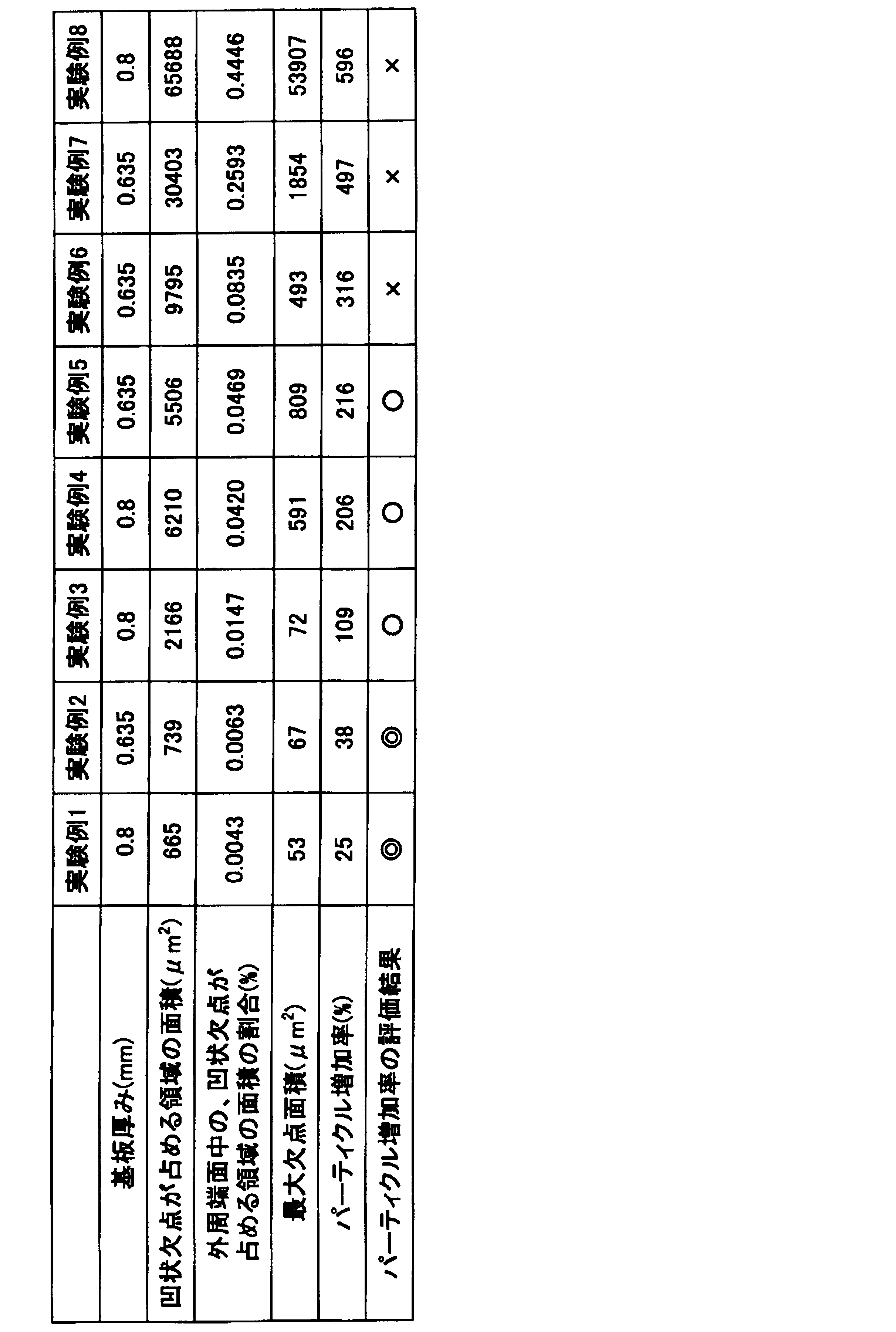
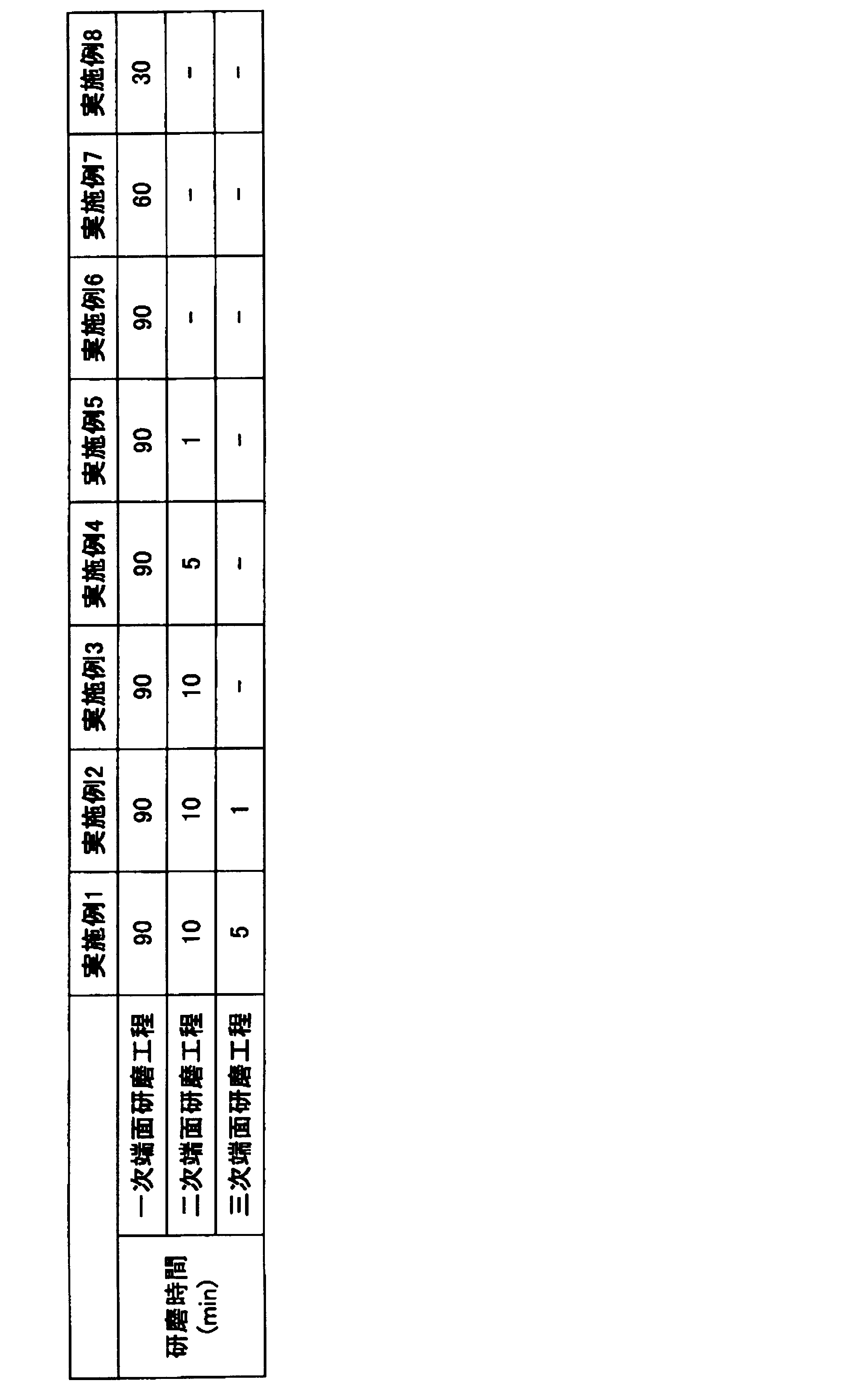
表1に示した結果によると、外周端面中の、凹状欠点が占める領域の面積の割合が0.05%以下である実験例1~実験例5は、いずれもパーティクル増加率は260%以下となっていることが確認できる。従って、外周端面の微小な疵に起因した、主表面への異物の付着を抑制できていることが確認できる。
これに対して、外周端面中の、凹状欠点が占める領域の面積の割合が0.05%を超える実験例6~実験例8については、いずれもパーティクル増加率は、260%を超え、外周端面の微小な疵に起因した、主表面への異物の付着を十分に抑制できていないことが確認できる。
また、実験例1~実験例5では、いずれも最大欠点面積が1000μm2以下であり、外周端面に含まれる個々の凹状欠点のサイズも小さいことが確認できる。
本発明を詳細に、また特定の実施態様を参照して説明したが、本発明の精神と範囲を逸脱することなく様々な変更や修正を加えることができることは当業者にとって明らかである。本出願は2015年12月28日出願の日本特許出願(特願2015-257145)、及び2016年4月11日出願の日本特許出願(特願2016-079173)に基づくものであり、その内容はここに参照として取り込まれる。
10 磁気記録媒体用ガラス基板
121、122 主表面
13 外周端面
131、133、221、223 外周面取り部
132、222 外周側面部
14 内周端面
23 凹状欠点
121、122 主表面
13 外周端面
131、133、221、223 外周面取り部
132、222 外周側面部
14 内周端面
23 凹状欠点
Claims (8)
- ドーナツ形状を有し、一対の主表面と、外周端面と、内周端面と、を有する磁気記録媒体用ガラス基板であって、
前記外周端面は外周側面部と一対の外周面取り部とを有し、
前記外周端面中の、凹状欠点が占める領域の面積の割合が0.05%以下である磁気記録媒体用ガラス基板。 - 前記外周端面中の、前記凹状欠点が占める領域の面積の割合が0.01%以下である請求項1に記載の磁気記録媒体用ガラス基板。
- 前記外周端面中の、前記凹状欠点が占める領域の面積の割合が0.005%以下である請求項1に記載の磁気記録媒体用ガラス基板。
- 前記外周端面中の、前記凹状欠点が占める領域の面積の割合は、
前記外周端面について、表面画像を得て、
前記表面画像中の、前記外周側面部、及び一対の前記外周面取り部に含まれる凹状欠点の明度と、前記凹状欠点以外の部分の明度とが分離できるように閾値を設け、
前記表面画像を前記閾値で二値化した、二値化処理済み表面画像を形成し、
前記二値化処理済み表面画像から算出する、請求項1乃至3のいずれか一項に記載の磁気記録媒体用ガラス基板。 - 前記外周端面が有する前記凹状欠点のうち、最も面積の大きい凹状欠点の面積である最大欠点面積が1000μm2以下である、請求項1乃至4のいずれか一項に記載の磁気記録媒体用ガラス基板。
- 前記最大欠点面積が100μm2以下である請求項5に記載の磁気記録媒体用ガラス基板。
- エネルギーアシスト磁気記録媒体用の磁気記録媒体用ガラス基板である、請求項1乃至6のいずれか一項に記載の磁気記録媒体用ガラス基板。
- 請求項1乃至7のいずれか一項に記載の磁気記録媒体用ガラス基板を含む磁気記録媒体。
Applications Claiming Priority (4)
| Application Number | Priority Date | Filing Date | Title |
|---|---|---|---|
| JP2015-257145 | 2015-12-28 | ||
| JP2015257145 | 2015-12-28 | ||
| JP2016-079173 | 2016-04-11 | ||
| JP2016079173A JP6020753B1 (ja) | 2015-12-28 | 2016-04-11 | 磁気記録媒体用ガラス基板、磁気記録媒体 |
Publications (1)
| Publication Number | Publication Date |
|---|---|
| WO2017115473A1 true WO2017115473A1 (ja) | 2017-07-06 |
Family
ID=57216828
Family Applications (1)
| Application Number | Title | Priority Date | Filing Date |
|---|---|---|---|
| PCT/JP2016/062148 Ceased WO2017115473A1 (ja) | 2015-12-28 | 2016-04-15 | 磁気記録媒体用ガラス基板及び磁気記録媒体 |
Country Status (2)
| Country | Link |
|---|---|
| JP (1) | JP6020753B1 (ja) |
| WO (1) | WO2017115473A1 (ja) |
Citations (7)
| Publication number | Priority date | Publication date | Assignee | Title |
|---|---|---|---|---|
| JPH08235543A (ja) * | 1995-03-01 | 1996-09-13 | Hitachi Ltd | 汚れ等の欠陥検出方法及び装置 |
| JPH0972722A (ja) * | 1995-09-07 | 1997-03-18 | Kao Corp | 基板外観検査装置 |
| JP2002168793A (ja) * | 2000-11-30 | 2002-06-14 | Fuji Photo Film Co Ltd | 表面欠陥検査装置および表面欠陥検査方法 |
| JP2012185891A (ja) * | 2011-03-07 | 2012-09-27 | Asahi Glass Co Ltd | 磁気記録媒体用ガラス基板の製造方法および磁気記録媒体用ガラス基板 |
| WO2014050241A1 (ja) * | 2012-09-28 | 2014-04-03 | Hoya株式会社 | 磁気ディスク用ガラス基板、磁気ディスク、磁気ディスク用ガラス基板の製造方法 |
| WO2014208717A1 (ja) * | 2013-06-27 | 2014-12-31 | Hoya株式会社 | 円板状ガラス基板、磁気ディスク用ガラス基板、磁気ディスク用ガラス基板の製造方法、磁気ディスク |
| JP2015069674A (ja) * | 2013-09-30 | 2015-04-13 | Hoya株式会社 | 磁気ディスク用ガラス基板の製造方法及び研磨処理用キャリア |
Family Cites Families (2)
| Publication number | Priority date | Publication date | Assignee | Title |
|---|---|---|---|---|
| JP4905238B2 (ja) * | 2007-04-27 | 2012-03-28 | コニカミノルタオプト株式会社 | 磁気記録媒体用ガラス基板の研磨方法 |
| JP2009035461A (ja) * | 2007-08-03 | 2009-02-19 | Asahi Glass Co Ltd | 磁気ディスク用ガラス基板の製造方法 |
-
2016
- 2016-04-11 JP JP2016079173A patent/JP6020753B1/ja active Active
- 2016-04-15 WO PCT/JP2016/062148 patent/WO2017115473A1/ja not_active Ceased
Patent Citations (7)
| Publication number | Priority date | Publication date | Assignee | Title |
|---|---|---|---|---|
| JPH08235543A (ja) * | 1995-03-01 | 1996-09-13 | Hitachi Ltd | 汚れ等の欠陥検出方法及び装置 |
| JPH0972722A (ja) * | 1995-09-07 | 1997-03-18 | Kao Corp | 基板外観検査装置 |
| JP2002168793A (ja) * | 2000-11-30 | 2002-06-14 | Fuji Photo Film Co Ltd | 表面欠陥検査装置および表面欠陥検査方法 |
| JP2012185891A (ja) * | 2011-03-07 | 2012-09-27 | Asahi Glass Co Ltd | 磁気記録媒体用ガラス基板の製造方法および磁気記録媒体用ガラス基板 |
| WO2014050241A1 (ja) * | 2012-09-28 | 2014-04-03 | Hoya株式会社 | 磁気ディスク用ガラス基板、磁気ディスク、磁気ディスク用ガラス基板の製造方法 |
| WO2014208717A1 (ja) * | 2013-06-27 | 2014-12-31 | Hoya株式会社 | 円板状ガラス基板、磁気ディスク用ガラス基板、磁気ディスク用ガラス基板の製造方法、磁気ディスク |
| JP2015069674A (ja) * | 2013-09-30 | 2015-04-13 | Hoya株式会社 | 磁気ディスク用ガラス基板の製造方法及び研磨処理用キャリア |
Also Published As
| Publication number | Publication date |
|---|---|
| JP2017120678A (ja) | 2017-07-06 |
| JP6020753B1 (ja) | 2016-11-02 |
Similar Documents
| Publication | Publication Date | Title |
|---|---|---|
| JP5035405B2 (ja) | 磁気記録媒体用ガラス基板の製造方法 | |
| JP5335789B2 (ja) | 磁気ディスク用基板及び磁気ディスク | |
| CN102820040B (zh) | 磁记录介质用玻璃基板、及使用该磁记录介质用玻璃基板的磁记录介质 | |
| WO2011125894A1 (ja) | 磁気ディスク用ガラス基板の製造方法 | |
| JP5635078B2 (ja) | 磁気ディスク用ガラス基板の製造方法 | |
| CN102930874B (zh) | 磁记录介质用玻璃基板 | |
| CN103978422A (zh) | 磁记录介质用玻璃基板的制造方法及磁记录介质用玻璃基板 | |
| JP2003346316A (ja) | 情報記録媒体並びに該情報記録媒体用ガラス基板の製造方法および該方法によって製造された情報記録媒体用ガラス基板 | |
| JP5915718B1 (ja) | 磁気ディスク用ガラス基板及び磁気ディスク | |
| JP5939350B1 (ja) | 磁気記録媒体用ガラス基板、磁気記録媒体 | |
| JP6020753B1 (ja) | 磁気記録媒体用ガラス基板、磁気記録媒体 | |
| JP6298448B2 (ja) | 磁気ディスク用ガラス基板の製造方法、磁気ディスク用ガラス基板、及び磁気ディスクの製造方法 | |
| JP6020754B1 (ja) | 磁気記録媒体用ガラス基板、磁気記録媒体 | |
| JP5494747B2 (ja) | 磁気記録媒体用ガラス基板の製造方法、及び、磁気記録媒体用ガラス基板 | |
| JP5212530B2 (ja) | 磁気記録媒体用ガラス基板、及び、該磁気記録媒体用ガラス基板を用いた磁気記録媒体 | |
| CN102855888B (zh) | 磁记录介质用玻璃基板及使用该磁记录介质用玻璃基板的磁记录介质 | |
| JP2012185891A (ja) | 磁気記録媒体用ガラス基板の製造方法および磁気記録媒体用ガラス基板 | |
| JP5983897B1 (ja) | 磁気ディスク用ガラス基板及び磁気ディスク | |
| JP5386037B2 (ja) | 磁気ディスク用ガラス基板の製造方法 | |
| JP5247141B2 (ja) | 磁気ディスク用ガラス基板の製造システム | |
| JP2012035330A (ja) | 磁気記録媒体用ガラス基板及びその製造方法 | |
| JP2013089280A (ja) | 磁気記録媒体用ガラス基板の製造方法、及び、磁気記録媒体の製造方法 | |
| JP2011076647A (ja) | 磁気ディスク用ガラス基板の製造方法 |
Legal Events
| Date | Code | Title | Description |
|---|---|---|---|
| 121 | Ep: the epo has been informed by wipo that ep was designated in this application |
Ref document number: 16881453 Country of ref document: EP Kind code of ref document: A1 |
|
| NENP | Non-entry into the national phase |
Ref country code: DE |
|
| 122 | Ep: pct application non-entry in european phase |
Ref document number: 16881453 Country of ref document: EP Kind code of ref document: A1 |