WO2017110291A1 - 計測センサ用パッケージおよび計測センサ - Google Patents
計測センサ用パッケージおよび計測センサ Download PDFInfo
- Publication number
- WO2017110291A1 WO2017110291A1 PCT/JP2016/083435 JP2016083435W WO2017110291A1 WO 2017110291 A1 WO2017110291 A1 WO 2017110291A1 JP 2016083435 W JP2016083435 W JP 2016083435W WO 2017110291 A1 WO2017110291 A1 WO 2017110291A1
- Authority
- WO
- WIPO (PCT)
- Prior art keywords
- housing recess
- light
- base body
- measurement sensor
- ground
- Prior art date
Links
- 239000004020 conductor Substances 0.000 claims abstract description 142
- 238000005259 measurement Methods 0.000 claims abstract description 76
- 239000000758 substrate Substances 0.000 claims description 20
- 229910010293 ceramic material Inorganic materials 0.000 claims description 7
- 239000011810 insulating material Substances 0.000 claims description 7
- 238000010030 laminating Methods 0.000 claims description 3
- 239000010410 layer Substances 0.000 description 58
- 239000000463 material Substances 0.000 description 16
- 230000017531 blood circulation Effects 0.000 description 14
- 230000000052 comparative effect Effects 0.000 description 13
- 239000011521 glass Substances 0.000 description 9
- 239000000919 ceramic Substances 0.000 description 7
- 229910052751 metal Inorganic materials 0.000 description 7
- 239000002184 metal Substances 0.000 description 7
- 239000011347 resin Substances 0.000 description 7
- 229920005989 resin Polymers 0.000 description 7
- 238000001228 spectrum Methods 0.000 description 7
- 238000005520 cutting process Methods 0.000 description 6
- 238000000034 method Methods 0.000 description 5
- XUIMIQQOPSSXEZ-UHFFFAOYSA-N Silicon Chemical compound [Si] XUIMIQQOPSSXEZ-UHFFFAOYSA-N 0.000 description 4
- 210000004369 blood Anatomy 0.000 description 4
- 239000008280 blood Substances 0.000 description 4
- 210000000601 blood cell Anatomy 0.000 description 4
- 230000000694 effects Effects 0.000 description 4
- 239000010703 silicon Substances 0.000 description 4
- 229910052710 silicon Inorganic materials 0.000 description 4
- PXHVJJICTQNCMI-UHFFFAOYSA-N Nickel Chemical compound [Ni] PXHVJJICTQNCMI-UHFFFAOYSA-N 0.000 description 3
- PNEYBMLMFCGWSK-UHFFFAOYSA-N aluminium oxide Inorganic materials [O-2].[O-2].[O-2].[Al+3].[Al+3] PNEYBMLMFCGWSK-UHFFFAOYSA-N 0.000 description 3
- 239000003822 epoxy resin Substances 0.000 description 3
- 238000011156 evaluation Methods 0.000 description 3
- 239000011368 organic material Substances 0.000 description 3
- 229920000647 polyepoxide Polymers 0.000 description 3
- 229910000679 solder Inorganic materials 0.000 description 3
- 239000010409 thin film Substances 0.000 description 3
- 229910045601 alloy Inorganic materials 0.000 description 2
- 239000000956 alloy Substances 0.000 description 2
- 239000000470 constituent Substances 0.000 description 2
- 238000010586 diagram Methods 0.000 description 2
- 229910052737 gold Inorganic materials 0.000 description 2
- 239000010931 gold Substances 0.000 description 2
- 238000004519 manufacturing process Methods 0.000 description 2
- 229910052759 nickel Inorganic materials 0.000 description 2
- 239000003960 organic solvent Substances 0.000 description 2
- 239000000843 powder Substances 0.000 description 2
- 239000002994 raw material Substances 0.000 description 2
- VYPSYNLAJGMNEJ-UHFFFAOYSA-N silicon dioxide Inorganic materials O=[Si]=O VYPSYNLAJGMNEJ-UHFFFAOYSA-N 0.000 description 2
- 239000002904 solvent Substances 0.000 description 2
- 238000004544 sputter deposition Methods 0.000 description 2
- 238000002834 transmittance Methods 0.000 description 2
- 229910052721 tungsten Inorganic materials 0.000 description 2
- 238000007740 vapor deposition Methods 0.000 description 2
- 239000004925 Acrylic resin Substances 0.000 description 1
- 229920000178 Acrylic resin Polymers 0.000 description 1
- 229910018072 Al 2 O 3 Inorganic materials 0.000 description 1
- 229910015363 Au—Sn Inorganic materials 0.000 description 1
- ODINCKMPIJJUCX-UHFFFAOYSA-N Calcium oxide Chemical compound [Ca]=O ODINCKMPIJJUCX-UHFFFAOYSA-N 0.000 description 1
- 239000004593 Epoxy Substances 0.000 description 1
- YCKRFDGAMUMZLT-UHFFFAOYSA-N Fluorine atom Chemical compound [F] YCKRFDGAMUMZLT-UHFFFAOYSA-N 0.000 description 1
- 229910001218 Gallium arsenide Inorganic materials 0.000 description 1
- 229910000530 Gallium indium arsenide Inorganic materials 0.000 description 1
- CPLXHLVBOLITMK-UHFFFAOYSA-N Magnesium oxide Chemical compound [Mg]=O CPLXHLVBOLITMK-UHFFFAOYSA-N 0.000 description 1
- 229910052581 Si3N4 Inorganic materials 0.000 description 1
- CDBYLPFSWZWCQE-UHFFFAOYSA-L Sodium Carbonate Chemical compound [Na+].[Na+].[O-]C([O-])=O CDBYLPFSWZWCQE-UHFFFAOYSA-L 0.000 description 1
- 230000004308 accommodation Effects 0.000 description 1
- 229910052782 aluminium Inorganic materials 0.000 description 1
- 210000004204 blood vessel Anatomy 0.000 description 1
- 239000005388 borosilicate glass Substances 0.000 description 1
- 238000005219 brazing Methods 0.000 description 1
- 239000003990 capacitor Substances 0.000 description 1
- 239000012671 ceramic insulating material Substances 0.000 description 1
- 229910052804 chromium Inorganic materials 0.000 description 1
- 229910052802 copper Inorganic materials 0.000 description 1
- PMHQVHHXPFUNSP-UHFFFAOYSA-M copper(1+);methylsulfanylmethane;bromide Chemical compound Br[Cu].CSC PMHQVHHXPFUNSP-UHFFFAOYSA-M 0.000 description 1
- 238000005260 corrosion Methods 0.000 description 1
- 230000007797 corrosion Effects 0.000 description 1
- KZHJGOXRZJKJNY-UHFFFAOYSA-N dioxosilane;oxo(oxoalumanyloxy)alumane Chemical compound O=[Si]=O.O=[Si]=O.O=[Al]O[Al]=O.O=[Al]O[Al]=O.O=[Al]O[Al]=O KZHJGOXRZJKJNY-UHFFFAOYSA-N 0.000 description 1
- 238000007606 doctor blade method Methods 0.000 description 1
- 238000001312 dry etching Methods 0.000 description 1
- 210000003743 erythrocyte Anatomy 0.000 description 1
- 239000000945 filler Substances 0.000 description 1
- 239000010408 film Substances 0.000 description 1
- 239000012530 fluid Substances 0.000 description 1
- 229910052731 fluorine Inorganic materials 0.000 description 1
- 239000011737 fluorine Substances 0.000 description 1
- 229910052732 germanium Inorganic materials 0.000 description 1
- GNPVGFCGXDBREM-UHFFFAOYSA-N germanium atom Chemical compound [Ge] GNPVGFCGXDBREM-UHFFFAOYSA-N 0.000 description 1
- 239000002241 glass-ceramic Substances 0.000 description 1
- PCHJSUWPFVWCPO-UHFFFAOYSA-N gold Chemical compound [Au] PCHJSUWPFVWCPO-UHFFFAOYSA-N 0.000 description 1
- 229910052738 indium Inorganic materials 0.000 description 1
- 238000005304 joining Methods 0.000 description 1
- 239000007769 metal material Substances 0.000 description 1
- 238000012986 modification Methods 0.000 description 1
- 230000004048 modification Effects 0.000 description 1
- 229910052863 mullite Inorganic materials 0.000 description 1
- TWNQGVIAIRXVLR-UHFFFAOYSA-N oxo(oxoalumanyloxy)alumane Chemical compound O=[Al]O[Al]=O TWNQGVIAIRXVLR-UHFFFAOYSA-N 0.000 description 1
- 229910052763 palladium Inorganic materials 0.000 description 1
- 238000000059 patterning Methods 0.000 description 1
- 239000005011 phenolic resin Substances 0.000 description 1
- 238000000206 photolithography Methods 0.000 description 1
- 238000007747 plating Methods 0.000 description 1
- 229910052697 platinum Inorganic materials 0.000 description 1
- 229920005668 polycarbonate resin Polymers 0.000 description 1
- 239000004431 polycarbonate resin Substances 0.000 description 1
- 229920001225 polyester resin Polymers 0.000 description 1
- 239000004645 polyester resin Substances 0.000 description 1
- 229920001721 polyimide Polymers 0.000 description 1
- 239000009719 polyimide resin Substances 0.000 description 1
- 239000010453 quartz Substances 0.000 description 1
- 238000005096 rolling process Methods 0.000 description 1
- 229910052707 ruthenium Inorganic materials 0.000 description 1
- 229910052594 sapphire Inorganic materials 0.000 description 1
- 239000010980 sapphire Substances 0.000 description 1
- 238000007650 screen-printing Methods 0.000 description 1
- 239000004065 semiconductor Substances 0.000 description 1
- HBMJWWWQQXIZIP-UHFFFAOYSA-N silicon carbide Chemical compound [Si+]#[C-] HBMJWWWQQXIZIP-UHFFFAOYSA-N 0.000 description 1
- 229910010271 silicon carbide Inorganic materials 0.000 description 1
- HQVNEWCFYHHQES-UHFFFAOYSA-N silicon nitride Chemical compound N12[Si]34N5[Si]62N3[Si]51N64 HQVNEWCFYHHQES-UHFFFAOYSA-N 0.000 description 1
- 229910052709 silver Inorganic materials 0.000 description 1
- 239000002356 single layer Substances 0.000 description 1
- 239000002002 slurry Substances 0.000 description 1
- 238000003860 storage Methods 0.000 description 1
- 229920005992 thermoplastic resin Polymers 0.000 description 1
- 229910052718 tin Inorganic materials 0.000 description 1
- 229910052719 titanium Inorganic materials 0.000 description 1
- WFKWXMTUELFFGS-UHFFFAOYSA-N tungsten Chemical compound [W] WFKWXMTUELFFGS-UHFFFAOYSA-N 0.000 description 1
- 239000010937 tungsten Substances 0.000 description 1
- 229920006337 unsaturated polyester resin Polymers 0.000 description 1
- 238000001039 wet etching Methods 0.000 description 1
Images


Classifications
-
- A—HUMAN NECESSITIES
- A61—MEDICAL OR VETERINARY SCIENCE; HYGIENE
- A61B—DIAGNOSIS; SURGERY; IDENTIFICATION
- A61B5/00—Measuring for diagnostic purposes; Identification of persons
- A61B5/02—Detecting, measuring or recording pulse, heart rate, blood pressure or blood flow; Combined pulse/heart-rate/blood pressure determination; Evaluating a cardiovascular condition not otherwise provided for, e.g. using combinations of techniques provided for in this group with electrocardiography or electroauscultation; Heart catheters for measuring blood pressure
- A61B5/026—Measuring blood flow
- A61B5/0261—Measuring blood flow using optical means, e.g. infrared light
-
- A—HUMAN NECESSITIES
- A61—MEDICAL OR VETERINARY SCIENCE; HYGIENE
- A61B—DIAGNOSIS; SURGERY; IDENTIFICATION
- A61B5/00—Measuring for diagnostic purposes; Identification of persons
- A61B5/0059—Measuring for diagnostic purposes; Identification of persons using light, e.g. diagnosis by transillumination, diascopy, fluorescence
-
- A—HUMAN NECESSITIES
- A61—MEDICAL OR VETERINARY SCIENCE; HYGIENE
- A61B—DIAGNOSIS; SURGERY; IDENTIFICATION
- A61B5/00—Measuring for diagnostic purposes; Identification of persons
- A61B5/02—Detecting, measuring or recording pulse, heart rate, blood pressure or blood flow; Combined pulse/heart-rate/blood pressure determination; Evaluating a cardiovascular condition not otherwise provided for, e.g. using combinations of techniques provided for in this group with electrocardiography or electroauscultation; Heart catheters for measuring blood pressure
- A61B5/026—Measuring blood flow
-
- A—HUMAN NECESSITIES
- A61—MEDICAL OR VETERINARY SCIENCE; HYGIENE
- A61B—DIAGNOSIS; SURGERY; IDENTIFICATION
- A61B5/00—Measuring for diagnostic purposes; Identification of persons
- A61B5/68—Arrangements of detecting, measuring or recording means, e.g. sensors, in relation to patient
- A61B5/6801—Arrangements of detecting, measuring or recording means, e.g. sensors, in relation to patient specially adapted to be attached to or worn on the body surface
- A61B5/6813—Specially adapted to be attached to a specific body part
- A61B5/6825—Hand
- A61B5/6826—Finger
-
- H—ELECTRICITY
- H01—ELECTRIC ELEMENTS
- H01L—SEMICONDUCTOR DEVICES NOT COVERED BY CLASS H10
- H01L23/00—Details of semiconductor or other solid state devices
- H01L23/58—Structural electrical arrangements for semiconductor devices not otherwise provided for, e.g. in combination with batteries
- H01L23/60—Protection against electrostatic charges or discharges, e.g. Faraday shields
-
- A—HUMAN NECESSITIES
- A61—MEDICAL OR VETERINARY SCIENCE; HYGIENE
- A61B—DIAGNOSIS; SURGERY; IDENTIFICATION
- A61B2562/00—Details of sensors; Constructional details of sensor housings or probes; Accessories for sensors
- A61B2562/18—Shielding or protection of sensors from environmental influences, e.g. protection from mechanical damage
- A61B2562/182—Electrical shielding, e.g. using a Faraday cage
-
- H—ELECTRICITY
- H01—ELECTRIC ELEMENTS
- H01L—SEMICONDUCTOR DEVICES NOT COVERED BY CLASS H10
- H01L2224/00—Indexing scheme for arrangements for connecting or disconnecting semiconductor or solid-state bodies and methods related thereto as covered by H01L24/00
- H01L2224/01—Means for bonding being attached to, or being formed on, the surface to be connected, e.g. chip-to-package, die-attach, "first-level" interconnects; Manufacturing methods related thereto
- H01L2224/42—Wire connectors; Manufacturing methods related thereto
- H01L2224/47—Structure, shape, material or disposition of the wire connectors after the connecting process
- H01L2224/48—Structure, shape, material or disposition of the wire connectors after the connecting process of an individual wire connector
- H01L2224/4805—Shape
- H01L2224/4809—Loop shape
- H01L2224/48091—Arched
-
- H—ELECTRICITY
- H01—ELECTRIC ELEMENTS
- H01L—SEMICONDUCTOR DEVICES NOT COVERED BY CLASS H10
- H01L2924/00—Indexing scheme for arrangements or methods for connecting or disconnecting semiconductor or solid-state bodies as covered by H01L24/00
- H01L2924/15—Details of package parts other than the semiconductor or other solid state devices to be connected
- H01L2924/161—Cap
- H01L2924/1615—Shape
- H01L2924/16195—Flat cap [not enclosing an internal cavity]
Definitions
- the present invention relates to a measurement sensor package and a measurement sensor.
- blood flow can be measured using the Doppler effect of light.
- light When light is irradiated to blood, light is scattered by blood cells such as red blood cells.
- the moving speed of the blood cell is calculated from the frequency of the irradiation light and the frequency of the scattered light.
- a measurement sensor that measures blood flow is described as, for example, a self-luminous measurement sensor in Patent Document 1, and an irradiation unit that irradiates light to blood and a light receiving unit that receives scattered light are arranged on a substrate.
- the front plate is bonded to the substrate by a light-shielding bonding portion that surrounds each.
- the tip of a finger which is a measurement location
- the human fingertip works like a capacitor, and when it touches the measurement sensor, the charge accumulated on the fingertip is released. Due to the discharge of this charge, noise is mixed in the current input to the light emitting element and the current output from the light receiving element, and the measurement accuracy is lowered due to the influence of this noise.
- the package for a measurement sensor includes a base, a lid, and a ground conductor layer.
- the base includes a base body and a ground via conductor.
- the base body is formed by laminating a plurality of dielectric layers, has a rectangular plate shape, and has a first housing recess for housing the light emitting element and a second housing recess for housing the light receiving element on the first surface. ing.
- the lid is a plate made of an insulating material that covers the first housing recess and the second housing recess, and the light emitted from the light emitting element housed in the first housing recess is transmitted therethrough, Light received by the light receiving element housed in the second housing recess is transmitted.
- the ground conductor layer is disposed on a surface of the lid that faces the first housing recess and the second housing recess, and is connected to a ground potential.
- the ground conductor layer is provided with a first opening through which light emitted from the light emitting element passes and a second opening through which light received by the light receiving element passes, and is electrically connected to the plurality of ground via conductors. Connected to.
- a measurement sensor includes the above-described measurement sensor package, a light emitting element accommodated in the first accommodating recess, and a light receiving element accommodated in the second accommodating recess.
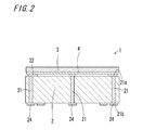
- FIG. 2 is a cross-sectional view taken along a cutting plane line AA of FIG.
- FIG. 2 is a cross-sectional view taken along a cutting plane line BB in FIG.
- FIG. 3 is a cross-sectional view of a measurement sensor package 1 ⁇ / b> A corresponding to the cross-sectional view shown in FIG. 2.
- FIG. 4 is a cross-sectional view of a measurement sensor package 1 ⁇ / b> A corresponding to the cross-sectional view shown in FIG. 3.
- 2 is a cross-sectional view illustrating a configuration of a measurement sensor 100.
- FIG. It is a figure which shows the measurement result of the power spectrum of an Example and a comparative example. It is a figure which shows the evaluation result of an Example and a comparative example.
- FIG. 1 is a plan view showing a measurement sensor package 1 according to an embodiment of the present invention
- FIG. 2 is a cross-sectional view taken along the section line AA of FIG. 1
- FIG. FIG. 6 is a cross-sectional view taken along the cutting plane line BB.
- the lid 3 is omitted.
- the measurement sensor package 1 includes a base 2, a lid 3 and a ground conductor layer 4.
- the base 2 contains a light emitting element and a light receiving element, and includes a base body 20, a plurality of ground via conductors 21, an annular ground conductor layer 22, a signal wiring conductor 23, and an external connection terminal 24. .
- the base body 20 of the present embodiment has a rectangular plate shape and is formed by laminating a plurality of dielectric layers.
- the base body 20 is provided with at least two recesses, and one of the two recesses is a first storage recess 20a for storing the light emitting element, and the other of the two recesses is It is the 2nd accommodation recessed part 20b which accommodates a light receiving element.
- the first housing recess 20 a and the second housing recess 20 b are provided so as to open on the same first surface (one main surface) of the base body 20.
- the measurement sensor package 1 of the present embodiment is suitably used as a measurement sensor that measures the flow of fluid such as blood flow by utilizing the Doppler effect of light.
- the measurement sensor includes a light emitting element that irradiates light to the object to be measured and a light receiving element that receives light scattered by the object to be measured.
- a part of the body such as a finger is irradiated with light from the outside, and light scattered by blood cells contained in blood flowing through the blood vessels under the skin is received, and the frequency Measure blood flow from changes.
- the light emitting element and the light receiving element are arranged at a predetermined interval based on the positional relationship between the irradiation light and the scattered light.
- the first housing recess 20a and the second housing recess 20b are provided according to the positional relationship of these elements.
- the size of the first receiving recess 20a and the size of the second receiving recess 20b may be appropriately set according to the size of the light emitting element and the light receiving element to be stored.
- the opening of the first housing recess 20a may be rectangular or square, for example.
- the size of the opening of the first housing recess 20a is, for example, a longitudinal length of 0.3 mm to 2.0 mm and a lateral length of 0.3 mm to 2.0 mm, and the depth of the first housing recess 20a. Is between 0.3 mm and 1.0 mm.
- the shape of the opening of the second housing recess 20b may be rectangular or square, for example.
- the size of the opening of the second housing recess 20b is, for example, a longitudinal length of 0.3 mm to 2.0 mm and a lateral length of 0.3 mm to 2.0 mm, and the depth of the second housing recess 20b. Is 0.4 mm to 1.5 mm.
- the opening shape of the first receiving recess 20a and the second receiving recess 20b may be, for example, a circular shape, a square shape, a rectangular shape, or other shapes.
- the first receiving recess 20a and the second receiving recess 20b may have a cross-sectional shape that is parallel to the main surface of the base body 20 and has a uniform shape in the depth direction.
- the first receiving recess 20a and the second receiving recess 20b have a uniform cross-sectional shape that is the same as the opening shape at a predetermined depth, and a cross-section after the predetermined depth. It may be a concave portion with a step whose shape is small and uniform to the bottom.
- a light emitting element or a light receiving element is mounted on the bottom of the recess, and a connection terminal for electrical connection with the light emitting element or the light receiving element is provided on the surface of the step. It is done.
- the ground via conductor 21 is a via conductor connected to the ground potential, and one or a plurality of the ground via conductors 21 are disposed outside the first housing recess 20a and the second housing recess 20b of the base body 20 in a plan view.
- the ground via conductor 21 includes a plurality of through conductors that penetrate through the dielectric layers constituting the base body 20 in the thickness direction in the thickness direction of the base body 20. In the present embodiment, for example, as shown in FIG. 2, the ground via conductor 21 penetrates the entire base body 20 in the thickness direction, and the position of the through conductor provided in each dielectric layer is the same in plan view. is there.
- the ground via conductor 21 penetrates in a straight line from one main surface of the base body 20 to the second surface (the other main surface), and one end surface 21 a of the ground via conductor 21 is one main surface of the base body 20.
- the other end surface 21 b is exposed on the other main surface of the base body 20.
- ground via conductor 21 One end surface 21a of the ground via conductor 21 is connected to a ground conductor layer disposed on the lid 3 via an annular ground conductor layer 22 described later.
- the other end surface 21 b of the ground via conductor 21 is connected to an external connection terminal 24 disposed on the other main surface of the base body 20.
- Such a ground via conductor 21 is electrically connected to the ground conductor layer, the annular ground conductor layer 22 and the ground via conductor 21 disposed on the lid 3 and is given the same ground potential.
- the electric charge emitted from a person is signal wiring from a connection body that electrically connects the light emitting element or the light receiving element and the measurement sensor package 1 such as a bonding wire. Enters the conductor and causes noise.
- the ground via conductor 21 forms a path in the measurement sensor package 1 through which charges discharged from a person easily flow, so that the charges are guided to the path and released to the outside. Prevents entry into the wiring conductor.
- the ground via conductor 21 is disposed along the outer shape of the base body 20. Since the base body 20 has a rectangular outer shape, the ground via conductor 21 is also disposed along the rectangular shape. That is, each ground via conductor 21 is arranged so that the distance from each side constituting the outline of the base body 20 to the ground via conductor 21 is the same. In the plan view of FIG. 1, the arrangement position of the ground via conductor 21 is indicated by a broken-line circle.
- the three ground via conductors 21 shown in the sectional view of FIG. 2 are the three ground via conductors 21 arranged at equal intervals in the horizontal direction on the upper side in FIG. Are arranged so that the imaginary straight line connecting them is parallel to the long side of the base body 20.
- ground via conductors 21 arranged in the vertical direction on the left side in the drawing have a virtual straight line connecting the centers parallel to the short side of the base body 20.
- the two ground via conductors 21 arranged horizontally in the lower side of the drawing are arranged so that a virtual straight line connecting the centers is parallel to the long side of the base body 20. .
- ground via conductors 21 surround the first housing recess 20a and the second housing recess 20b outside the first housing recess 20a and the second housing recess 20b, and the base body. 20 are arranged along a rectangle which is the outer shape. Of the four corners of the rectangle, ground via conductors 21 are disposed at three corners, respectively, and are not disposed at the remaining one corner.
- the arrangement position of the ground via conductor 21 is determined based on the distance from the first housing recess 20a and the distance from the second housing recess 20b. As described above, since unnecessary electric charge that causes noise flows into the ground via conductor 21 when entering the signal wiring conductor, the ground via conductor 21 and the signal wiring formed in the measurement sensor package 1 are used. The distance from the conductor 23 (including the inside of the base body 20 and the bonding wire) is made larger than a predetermined distance to reduce unnecessary charges from entering the signal wiring conductor 23 from the ground via conductor 21. .
- the ground via is located at a position where the distance from the first receiving recess 20a or the second receiving recess 20b, in other words, the distance from the signal wiring conductor 23 is smaller than a predetermined distance.
- the conductor 21 may not be provided.
- the ground via conductor 21 is not provided at one corner because the distance between the corner and the signal wiring conductor 23 is smaller than a predetermined distance.
- the ground via conductor 21 may have a low electrical resistance in order to induce unnecessary charges as described above to be released to the outside of the package. To reduce the electrical resistance, the ground via conductor 21 may have a larger diameter. Good. However, if the diameter is too large, the distance from the signal wiring conductor is reduced, and unnecessary charges may enter the signal wiring conductor from the ground via conductor 21. Therefore, considering these, for example, the size of the ground via conductor 21 may be such that the diameter D is 10 ⁇ m to 500 ⁇ m.
- the annular ground conductor layer 22 is a conductor layer provided in an annular shape on one main surface of the base body 20 so as to surround the opening of the first housing recess 20a and the opening of the second housing recess 20b.
- the annular conductor layer electrically connects each end face 21 a of the ground via conductor 21 exposed on the one main surface of the base body 20.
- the annular grounding conductor layer 22 is used for joining the lid 3 to the base body 2, such as solder, Au—Sn, brazing filler metal or other molten metal joint material, or epoxy, silicon, thermoplastic resin, anisotropic
- the ground conductor layer 4 is joined by a resin-based joining material such as a conductive resin, a conductive epoxy resin, or a conductive silicon resin.
- the plurality of ground via conductors 21 are disposed along a rectangle that is the outer shape of the base body 20, and each one end surface 21 a is also formed on one main surface of the base body 20 along the rectangle that is the outer shape of the base body 20. Exposed.
- the annular ground conductor layer 22 for electrically connecting the respective one end faces 21 a is also provided in a rectangular shape according to the arrangement positions thereof.
- the annular ground conductor layer 22 has a land portion 22a connected to one end face 21a of the ground via conductor 21, and a connection line portion 22b connecting each land portion 22a.
- the land portion 22a is formed larger than the one end surface 21a in order to reliably connect with the one end surface 21a of the ground via conductor 21 with low resistance.
- the land portion 22a has a width or diameter of 1 ⁇ D to 3 ⁇ D (1 to 3 times the diameter) with respect to the diameter D of the one end face 21a of the ground via conductor 21.
- the connection line portion 22b is thinner than the land portion 22a and has a constant line width.
- the signal wiring conductor 23 is electrically connected to the light emitting element or the light receiving element, the electric signal input to the light emitting element is transmitted, and the electric signal output from the light receiving element is transmitted.
- the signal wiring conductor 23 in this embodiment includes a bonding wire that is a connection member connected to the light emitting element or the light receiving element, a connection pad 23a to which the bonding wire is connected, and a connection pad 23a that is electrically connected to the connection pad 23a.
- the signal via conductor 23 b extends in a straight line from directly below to the other main surface of the base body 20 and an external connection terminal 24.
- the external connection terminal 24 is electrically connected to a connection terminal of an external mounting substrate on which the measurement sensor including the measurement sensor package 1 is mounted by a bonding material such as solder.
- the annular ground conductor layer 22 and the external connection terminal 24 are, for example, a nickel layer having a thickness of 0.5 to 10 ⁇ m and a thickness of 0 in order to improve wettability with a bonding material such as solder and improve corrosion resistance.
- a gold layer of 5 to 5 ⁇ m may be sequentially deposited by a plating method.
- the dielectric layer of the base body 20 is made of a ceramic insulating material.
- the signal wiring conductor 23 and the like may be a ceramic wiring board made of a conductive material, and the dielectric layer may be an organic wiring board made of a resin insulating material.
- each conductor is formed on a dielectric layer made of a ceramic material.
- the ceramic wiring board is formed from a plurality of ceramic dielectric layers.
- Examples of the ceramic material used in the ceramic wiring board include an aluminum oxide sintered body, a mullite sintered body, a silicon carbide sintered body, an aluminum nitride sintered body, a silicon nitride sintered body, or a glass ceramic sintered body. A ligature etc. are mentioned.
- the substrate 2 is an organic wiring substrate
- a wiring conductor is formed on an insulating layer made of an organic material.
- the organic wiring board is formed from a plurality of organic dielectric layers.
- the organic wiring substrate may be any material in which a dielectric layer such as a printed wiring substrate, a build-up wiring substrate, or a flexible wiring substrate is made of an organic material.
- a dielectric layer such as a printed wiring substrate, a build-up wiring substrate, or a flexible wiring substrate is made of an organic material.
- the organic material used in the organic wiring board include an epoxy resin, a polyimide resin, a polyester resin, an acrylic resin, a phenol resin, and a fluorine resin.
- the lid 3 is joined to one main surface of the base body 20 and covers the first housing recess 20a and the second housing recess 20b.
- the lid 3 is a plate-like member made of an insulating material.
- the lid 3 is configured such that light emitted from the light emitting element accommodated in the first accommodating recess 20a is transmitted and light received by the light receiving element accommodated in the second accommodating recess 20b is transmitted.
- the surface of the lid 3 is irradiated with light emitted from the light emitting element in a state where, for example, a finger as a measurement object is applied.
- the lid 3 is made of a conductive material, when the finger is brought into contact with the lid 3, the above-mentioned unnecessary charges are released from the finger, and the charge flows into the base 2 through the lid 3 and noise. Occurs.
- the lid 3 By configuring the lid 3 with an insulating material, it is possible to prevent unnecessary charges from flowing through the lid 3.
- the lid 3 needs to transmit the irradiation light and scattered light to the object to be measured. Since the characteristics of the irradiation light and the scattered light are determined by the light emitting element to be mounted, it is sufficient that the lid 3 is configured to transmit at least light emitted from the light emitting element to be mounted.
- the insulating material constituting the lid 3 may have a transmittance of light of the wavelength of 70% or more with respect to the wavelength of light emitted from the light emitting element, and has a transmittance of 90% or more. It is preferable.
- a transparent ceramic material such as sapphire, a glass material or a resin material
- a glass material borosilicate glass, crystallized glass, quartz, soda glass, or the like
- the resin material polycarbonate resin, unsaturated polyester resin, epoxy resin, or the like can be used.
- the lid 3 requires a predetermined strength because an object to be measured such as a finger is in direct contact.
- the strength of the lid 3 depends on the strength and thickness of the constituent material. If it is a transparent ceramic material and a glass material as mentioned above, sufficient intensity
- the ground conductor layer 4 is disposed on the main surface of the lid 3 that faces the first receiving recess 20a and the second receiving recess 20b, that is, the main surface that is opposite to the main surface that contacts the fingers. , Connected to ground potential.
- the ground conductor layer 4 is provided with a first opening 4a through which light emitted from the light emitting element passes and a second opening 4b through which light received by the light receiving element passes, and is electrically connected to the plurality of ground via conductors 21. Connected to.
- the ground conductor layer 4 has the first opening 4a and the second opening 4b so that unnecessary light is not emitted from the first housing recess 20a to the outside and so that unnecessary light does not enter the second housing recess 20b from the outside. It functions as a provided mask member.
- the ground conductor layer 4 also functions as an electromagnetic shield for suppressing electromagnetic waves coming from the outside from entering the first housing recess 20a and the second housing recess 20b.
- the signal wiring conductor 23, particularly the bonding wire receives the entering electromagnetic wave as an antenna and causes noise.
- the influence of noise can be suppressed and the measurement accuracy can be improved.
- the ground conductor layer 4 is electrically connected to the ground via conductor 21 and the annular ground conductor layer 22 and given a ground potential.
- the lid 3 made of a transparent ceramic material or a glass material.
- Metal materials such as Ni, W, and alloys thereof, and alloys thereof can be formed as a metal thin film by vapor deposition, sputtering, baking, or the like.
- the layer thickness of the ground conductor layer 4 is, for example, 500 mm to 4000 mm.
- the ground conductor layer 4 may be a single layer or may be formed by overlapping a plurality of layers.
- FIG. 4 is a cross-sectional view of the measurement sensor package 1A corresponding to the cross-sectional view shown in FIG. 2
- FIG. 5 is a cross-sectional view of the measurement sensor package 1A corresponding to the cross-sectional view shown in FIG.
- the measurement sensor package 1A of the present embodiment is different from the measurement sensor package 1 of the above-described embodiment in that the base 2 further includes an internal ground conductor layer 25, and the other configurations are the same. Therefore, the same reference numerals as those of the measurement sensor package 1 are attached to the same components, and detailed description thereof is omitted.
- the internal ground conductor layer 25 is connected to the ground potential, and is disposed between the bottom of the second housing recess 20b and the other main surface of the base body 20.
- the internal ground conductor layer 25 is electrically connected to the ground via conductor 21 inside the base body 20 and is applied with a ground potential.
- the amount of light received by the light receiving element is relatively small, so the electrical signal output from the light receiving element is weak and noise compared to the electrical signal for light emission control input to the light emitting element. It is greatly affected by.
- the measurement sensor is mounted and used on an external mounting board, and electromagnetic waves caused by signals flowing through the wiring of the external mounting board enter the measurement sensor package 1 from the other main surface side of the base body 20. As a result, noise may be mixed in the signal flowing through the signal wiring conductor 23.
- the bottom and the other main surface of the second housing recess 20b in which the light receiving element is housed In order to suppress the influence of noise from the external mounting substrate, the bottom and the other main surface of the second housing recess 20b in which the light receiving element is housed.
- An internal ground conductor layer 25 is provided between the two.
- the internal ground conductor layer 25 is positioned between the second housing recess 20b and the external mounting substrate, and functions as an electromagnetic shield.
- the measurement sensor package 1A of the present embodiment includes the internal ground conductor layer 25, thereby suppressing the influence of noise and further improving the measurement accuracy.
- the base body 2 is produced in the same manner as a known multilayer wiring board manufacturing method.
- the substrate 2 is a ceramic wiring board and the ceramic material is alumina
- it is suitable for a raw material powder such as alumina (Al 2 O 3 ), silica (SiO 2 ), calcia (CaO), magnesia (MgO), etc.
- An organic solvent and a solvent are added and mixed to form a slurry, which is formed into a sheet by a known doctor blade method, calendar roll method, or the like to obtain a ceramic green sheet (hereinafter also referred to as a green sheet).
- the green sheet is punched into a predetermined shape, and an organic solvent and a solvent are added to and mixed with the raw material powder such as tungsten (W) and a glass material to form a metal paste.
- the via conductor is provided with a through hole in the green sheet, and the metal paste is filled into the through hole by screen printing or the like.
- a plurality of the green sheets obtained in this way are stacked, and these are co-fired at a temperature of about 1600 ° C., thereby producing the substrate 2.
- a lid 3 obtained by cutting a glass material into a predetermined shape by cutting, cutting or the like is prepared, and a ground conductor layer 4 made of a metal thin film is formed on the main surface by vapor deposition, sputtering, baking, or the like.
- the first opening 4a and the second opening 4b can be formed by patterning the metal thin film by a photolithography (wet etching) method, a dry etching method, or the like.
- FIG. 6 is a cross-sectional view showing the configuration of the measurement sensor 100.
- the measurement sensor 100 includes the above-described measurement sensor packages 1 and 1A, the light emitting element 30 accommodated in the first accommodating recess 20a, and the light receiving element 31 accommodated in the second accommodating recess 20b.
- the light emitting element 30 and the light receiving element 31 are mounted on the measurement sensor package 1, these elements are connected to the connection pads 23 a by the bonding wires 32, and then the lid 3 is bonded to the base body 20. Obtained.
- the light emitting element 30 can be a semiconductor laser element such as a VCSEL, and the light receiving element 31 can be a variety of photodiodes such as a silicon photodiode, a GaAs photodiode, an InGaAs photodiode, or a germanium photodiode.
- the light emitting element 30 and the light receiving element 31 may be appropriately selected depending on the type of the object to be measured, the type of parameter to be measured, and the like.
- the VCSEL that is the light emitting element 30 When measuring the blood flow, for example, as long as the VCSEL that is the light emitting element 30 is capable of emitting laser light having a wavelength of 850 nm in order to measure using the Doppler effect of light.
- the light emitting element 30 that emits laser light having a wavelength according to the measurement purpose may be selected.
- the light receiving element 31 may be any element that can receive the light emitted from the light emitting element 30 when the received light has no wavelength change from the laser light emitted from the light emitting element 30. If there is a wavelength change, It is sufficient if it can receive light of a wavelength of.
- the light emitting element 30, the light receiving element 31, and the connection pad 23a are electrically connected by, for example, the bonding wire 32, but flip chip connection, bump connection, connection using an anisotropic conductive film, or the like. Other connection methods may be used.
- the measurement sensor 100 is used by being mounted on an external mounting board.
- an external mounting substrate for example, a control element that controls light emission of the light emitting element 30, an arithmetic element that calculates a blood flow velocity and the like from an output signal of the light receiving element 31, and the like are mounted.
- a light emitting element control current is input from the external mounting substrate to the measurement sensor 100 via the external connection terminal 24 with the fingertip of the finger as the object to be measured being in contact with the surface of the lid 3.
- Light is input to the light emitting element 30 through the via conductor 23 b and the connection pad 23 a, and measurement light is emitted from the light emitting element 30.
- the emitted light passes through the first opening 4a, passes through the lid 3 and is irradiated onto the fingertip, it is scattered by blood cells in the blood.
- an electrical signal corresponding to the amount of received light is output from the light receiving element 31.
- the output signal passes through the connection pad 23a and the signal via conductor 23b, and is output from the measurement sensor 100 to the external mounting board via the external connection terminal 24.
- the signal output from the measurement sensor 100 is input to the arithmetic element, and for example, the frequency of the irradiation light that is the light emitted from the light emitting element 30 and the scattered light that is the light received by the light receiving element 31.
- the blood flow velocity can be calculated on the basis of the frequency.
- the ground via conductor 21 is configured to be formed in a straight line in the vertical direction within the base body 20, but electrically from one main surface of the base body 20 to the external connection terminal 24 on the other main surface. As long as they are connected, they may not be straight, but may be shifted in the base body 20 by the inner layer wiring, the inner ground conductor layer 25, or the like.
- the annular ground conductor layer 22 is not an essential component, and is configured so that the ground conductor layer 4 formed on the lid 3 and the ground via conductor 21 are directly joined and electrically connected. May be.
- the internal ground conductor layer 25 further extends in the surface direction from between the bottom of the second housing recess 20b and the other main surface of the base body 20, and between the bottom of the first housing recess 20a and the other main surface. It may be arranged.
- a measurement sensor package (dielectric layer is made of alumina, length 3 mm, width 4.5 mm, thickness 1.2 mm) having the same configuration as the measurement sensor package 1 shown in FIGS.
- a VCSEL having a near-infrared wavelength and a silicon photodiode having a light receiving diameter of ⁇ 200 ⁇ m as the light receiving element 31 are mounted in a measurement sensor package to obtain a measurement sensor according to an embodiment of the present invention.
- a measurement sensor of a comparative example was obtained in the same manner as in the example except that the ground via conductor 21 was not provided.
- the power spectrum was measured as follows. The light generated from the VCSEL is irradiated on the object to be measured, and the current generated by receiving the diffused light returned by the photodiode is used as an output signal. Since the output signal is weak, it was amplified using an amplifier circuit, then AD (analog-digital) converted, and the converted digital signal was Fourier transformed to obtain a power spectrum.
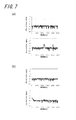
- FIG. 7 is a diagram showing measurement results of the power spectrum of the example and the comparative example.
- Fig.7 (a) shows the result of a comparative example
- FIG.7 (b) shows the result of an Example.
- the upper graph is a result in a state where the finger is not brought into contact with the lid 3
- the lower graph is a result in a state where the finger is brought into contact with the lid.
- noise was generated at frequencies of 9 kHz to 10 kHz and 16 kHz when the finger was in contact.
- no output change was observed below 2 kHz due to scattering by blood flow that should be detected.
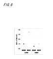
- FIG. 8 is a diagram showing the evaluation results of Examples and Comparative Examples.
- the maximum noise amount was used as the evaluation result.
- the maximum noise amount is calculated by the difference between the maximum output value and the minimum output value at a frequency of 2 kHz or more in the power spectrum. It can be evaluated that the larger the maximum amount of noise is, the more remarkable the occurrence of noise is, and the smaller the maximum amount of noise is, the more suppressed the generation of noise.
- the maximum noise amount is small in both the example and the comparative example, and the example is smaller than the comparative example. It can be seen that minute noise in a state in which is not in contact with the lid 3 is also suppressed. In addition, the maximum noise amount in the comparative example was larger in the state where the finger was in contact with the lid 3 than in the state where the finger was not in contact, whereas it was only slightly larger in the example.
Abstract
Description
2 基体
3 蓋体
4 接地導体層
4a 第1開口
4b 第2開口
20 基体本体
20a 第1収容凹部
20b 第2収容凹部
21 接地ビア導体
21a 一方端面
21b 他方端面
22 環状接地導体層
22a ランド部分
22b 接続線部分
23 信号配線導体
23a 接続パッド
23b 信号ビア導体
24 外部接続端子
25 内部接地導体層
30 発光素子
31 受光素子
32 ボンディングワイヤ
100 計測センサ
Claims (5)
- 複数の誘電体層が積層されて成る、矩形板状の基体本体であって、発光素子を収容する第1収容凹部および受光素子を収容する第2収容凹部が、第1面に設けられている基体本体と、平面視で、該基体本体の、前記第1収容凹部および前記第2収容凹部よりも外方に配設され、接地電位に接続される1または複数の接地ビア導体と、を有する基体と、
前記第1収容凹部および前記第2収容凹部を覆う、絶縁材料からなる板状の蓋体であって、前記第1収容凹部に収容される前記発光素子から出射される光が透過し、前記第2収容凹部に収容される前記受光素子が受光する光が透過する蓋体と、
該蓋体の、前記第1収容凹部および前記第2収容凹部に対向する側の面に配設される、接地電位に接続される接地導体層であって、前記発光素子から出射される光が通過する第1開口および前記受光素子が受光する光が通過する第2開口が設けられており、前記複数の接地ビア導体と電気的に接続される接地導体層と、を含むことを特徴とする計測センサ用パッケージ。 - 前記基体には、接地ビア導体が複数配設され
複数の接地ビア導体は、前記基体本体の第1面の外周に沿って配設され、一方の端面がそれぞれ前記基体の第1面に露出しており、
前記基体は、前記基体本体の前記第1面に、前記第1収容凹部の開口および前記第2収容凹部の開口を取り囲むように環状に設けられる、前記複数の接地ビア導体の各一方の端面を電気的に接続する環状導体層を有することを特徴とする請求項1記載の計測センサ用パッケージ。 - 前記基体は、前記基体本体の、前記第2収容凹部の底部と前記第1面とは反対側の第2面との間に配設される、接地電位に接続される内部接地導体層を有することを特徴とする請求項1または2記載の計測センサ用パッケージ。
- 前記誘電体層は、セラミックス材料を含むことを特徴とする請求項1~3のいずれか1つに記載の計測センサ用パッケージ。
- 請求項1~4のいずれか1つに記載の計測センサ用パッケージと、
前記第1収容凹部に収容される発光素子と、
前記第2収容凹部に収容される受光素子と、を含むことを特徴とする計測センサ。
Priority Applications (6)
| Application Number | Priority Date | Filing Date | Title |
|---|---|---|---|
| US15/770,658 US11166642B2 (en) | 2015-12-22 | 2016-11-10 | Measurement sensor package and measurement sensor |
| EP21205560.2A EP4026493A1 (en) | 2015-12-22 | 2016-11-10 | Measuring sensor package and measurement sensor |
| CN201680060515.8A CN108135516B (zh) | 2015-12-22 | 2016-11-10 | 测量传感器用封装体以及测量传感器 |
| JP2017557785A JP6483859B2 (ja) | 2015-12-22 | 2016-11-10 | 計測センサ用パッケージおよび計測センサ |
| EP16878189.6A EP3395242B1 (en) | 2015-12-22 | 2016-11-10 | Measuring sensor package and measuring sensor |
| KR1020187010706A KR102136538B1 (ko) | 2015-12-22 | 2016-11-10 | 계측 센서용 패키지 및 계측 센서 |
Applications Claiming Priority (2)
| Application Number | Priority Date | Filing Date | Title |
|---|---|---|---|
| JP2015250656 | 2015-12-22 | ||
| JP2015-250656 | 2015-12-22 |
Publications (1)
| Publication Number | Publication Date |
|---|---|
| WO2017110291A1 true WO2017110291A1 (ja) | 2017-06-29 |
Family
ID=59090416
Family Applications (1)
| Application Number | Title | Priority Date | Filing Date |
|---|---|---|---|
| PCT/JP2016/083435 WO2017110291A1 (ja) | 2015-12-22 | 2016-11-10 | 計測センサ用パッケージおよび計測センサ |
Country Status (6)
| Country | Link |
|---|---|
| US (1) | US11166642B2 (ja) |
| EP (2) | EP4026493A1 (ja) |
| JP (1) | JP6483859B2 (ja) |
| KR (1) | KR102136538B1 (ja) |
| CN (2) | CN108135516B (ja) |
| WO (1) | WO2017110291A1 (ja) |
Cited By (1)
| Publication number | Priority date | Publication date | Assignee | Title |
|---|---|---|---|---|
| WO2020090883A1 (ja) * | 2018-10-30 | 2020-05-07 | 京セラ株式会社 | 光学センサ装置 |
Families Citing this family (2)
| Publication number | Priority date | Publication date | Assignee | Title |
|---|---|---|---|---|
| EP3410127A4 (en) * | 2016-01-25 | 2019-08-28 | Kyocera Corporation | MEASUREMENT SENSOR HOUSING, AND MEASUREMENT SENSOR |
| US10582864B2 (en) * | 2016-04-04 | 2020-03-10 | Kyocera Corporation | Measurement sensor package and measurement sensor |
Citations (5)
| Publication number | Priority date | Publication date | Assignee | Title |
|---|---|---|---|---|
| JPS5146596B2 (ja) * | 1972-09-06 | 1976-12-09 | ||
| JPS63194638A (ja) * | 1987-02-10 | 1988-08-11 | 松下電器産業株式会社 | 光電式脈波検出器 |
| JP2001284488A (ja) * | 2000-03-30 | 2001-10-12 | Ngk Spark Plug Co Ltd | 配線基板 |
| JP2004041482A (ja) * | 2002-07-12 | 2004-02-12 | Seiko Epson Corp | 脈波検出装置及び生体電位検出装置 |
| JP2005260877A (ja) * | 2004-03-15 | 2005-09-22 | Kyocera Corp | 高周波モジュール及び無線通信装置 |
Family Cites Families (20)
| Publication number | Priority date | Publication date | Assignee | Title |
|---|---|---|---|---|
| JPS5031895B1 (ja) | 1971-03-16 | 1975-10-16 | ||
| US6300659B1 (en) * | 1994-09-30 | 2001-10-09 | Semiconductor Energy Laboratory Co., Ltd. | Thin-film transistor and fabrication method for same |
| KR100309957B1 (ko) * | 1997-09-08 | 2002-08-21 | 신꼬오덴기 고교 가부시키가이샤 | 반도체장치 |
| US6486534B1 (en) * | 2001-02-16 | 2002-11-26 | Ashvattha Semiconductor, Inc. | Integrated circuit die having an interference shield |
| JP4061409B2 (ja) * | 2004-11-09 | 2008-03-19 | 国立大学法人九州大学 | センサ部及び生体センサ |
| CN2879968Y (zh) * | 2006-02-17 | 2007-03-21 | 杭州大力神医疗器械有限公司 | 光电指脉传感器 |
| JP4708214B2 (ja) * | 2006-02-23 | 2011-06-22 | 浜松ホトニクス株式会社 | 光送受信デバイス |
| JP5031895B2 (ja) | 2008-05-12 | 2012-09-26 | パイオニア株式会社 | 自発光型センサ装置及びその製造方法 |
| CN102026575B (zh) * | 2008-05-12 | 2013-12-18 | 日本先锋公司 | 自发光传感器装置 |
| JP5549104B2 (ja) * | 2008-05-29 | 2014-07-16 | 株式会社リコー | 発光装置、光走査装置及び画像形成装置 |
| WO2010003134A2 (en) * | 2008-07-03 | 2010-01-07 | Masimo Laboratories, Inc. | Protrusion, heat sink, and shielding for improving spectroscopic measurement of blood constituents |
| KR101307212B1 (ko) | 2009-04-30 | 2013-09-11 | 가부시키가이샤 무라타 세이사쿠쇼 | 생체 센서 장치 |
| JP2010264174A (ja) * | 2009-05-18 | 2010-11-25 | Hitachi Cable Ltd | 表面筋電位センサ |
| US8199518B1 (en) * | 2010-02-18 | 2012-06-12 | Amkor Technology, Inc. | Top feature package and method |
| US8258012B2 (en) * | 2010-05-14 | 2012-09-04 | Stats Chippac, Ltd. | Semiconductor device and method of forming discontinuous ESD protection layers between semiconductor die |
| US9490239B2 (en) * | 2011-08-31 | 2016-11-08 | Micron Technology, Inc. | Solid state transducers with state detection, and associated systems and methods |
| TWI453923B (zh) * | 2012-06-22 | 2014-09-21 | Txc Corp | Light sensing chip package structure |
| PL2931121T3 (pl) * | 2012-12-14 | 2017-08-31 | Koninklijke Philips N.V. | Urządzenie do pomiaru parametru fizjologicznego użytkownika |
| EP2803315B1 (en) * | 2013-05-15 | 2019-10-02 | Polar Electro Oy | Heart activity sensor structure |
| JP5907200B2 (ja) * | 2014-03-18 | 2016-04-26 | セイコーエプソン株式会社 | 光検出ユニット及び生体情報検出装置 |
-
2016
- 2016-11-10 CN CN201680060515.8A patent/CN108135516B/zh active Active
- 2016-11-10 CN CN202011206741.7A patent/CN112168146A/zh active Pending
- 2016-11-10 KR KR1020187010706A patent/KR102136538B1/ko active IP Right Grant
- 2016-11-10 EP EP21205560.2A patent/EP4026493A1/en not_active Withdrawn
- 2016-11-10 WO PCT/JP2016/083435 patent/WO2017110291A1/ja active Application Filing
- 2016-11-10 US US15/770,658 patent/US11166642B2/en active Active
- 2016-11-10 JP JP2017557785A patent/JP6483859B2/ja active Active
- 2016-11-10 EP EP16878189.6A patent/EP3395242B1/en active Active
Patent Citations (5)
| Publication number | Priority date | Publication date | Assignee | Title |
|---|---|---|---|---|
| JPS5146596B2 (ja) * | 1972-09-06 | 1976-12-09 | ||
| JPS63194638A (ja) * | 1987-02-10 | 1988-08-11 | 松下電器産業株式会社 | 光電式脈波検出器 |
| JP2001284488A (ja) * | 2000-03-30 | 2001-10-12 | Ngk Spark Plug Co Ltd | 配線基板 |
| JP2004041482A (ja) * | 2002-07-12 | 2004-02-12 | Seiko Epson Corp | 脈波検出装置及び生体電位検出装置 |
| JP2005260877A (ja) * | 2004-03-15 | 2005-09-22 | Kyocera Corp | 高周波モジュール及び無線通信装置 |
Non-Patent Citations (1)
| Title |
|---|
| See also references of EP3395242A4 * |
Cited By (4)
| Publication number | Priority date | Publication date | Assignee | Title |
|---|---|---|---|---|
| WO2020090883A1 (ja) * | 2018-10-30 | 2020-05-07 | 京セラ株式会社 | 光学センサ装置 |
| CN112912984A (zh) * | 2018-10-30 | 2021-06-04 | 京瓷株式会社 | 光学传感器装置 |
| JPWO2020090883A1 (ja) * | 2018-10-30 | 2021-10-14 | 京セラ株式会社 | 光学センサ装置 |
| JP7134246B2 (ja) | 2018-10-30 | 2022-09-09 | 京セラ株式会社 | 光学センサ装置 |
Also Published As
| Publication number | Publication date |
|---|---|
| US11166642B2 (en) | 2021-11-09 |
| CN112168146A (zh) | 2021-01-05 |
| CN108135516B (zh) | 2020-11-20 |
| JP6483859B2 (ja) | 2019-03-13 |
| EP4026493A1 (en) | 2022-07-13 |
| EP3395242A4 (en) | 2019-09-04 |
| EP3395242B1 (en) | 2021-11-10 |
| EP3395242A1 (en) | 2018-10-31 |
| KR20180053383A (ko) | 2018-05-21 |
| KR102136538B1 (ko) | 2020-07-22 |
| US20180310836A1 (en) | 2018-11-01 |
| CN108135516A (zh) | 2018-06-08 |
| JPWO2017110291A1 (ja) | 2018-08-16 |
Similar Documents
| Publication | Publication Date | Title |
|---|---|---|
| JP7061990B2 (ja) | 計測センサ用パッケージおよび計測センサ | |
| JP6483859B2 (ja) | 計測センサ用パッケージおよび計測センサ | |
| JP6659377B2 (ja) | 計測センサ用パッケージおよび計測センサ | |
| JP6999407B2 (ja) | 光学センサ装置 | |
| JP2018100934A (ja) | センサ装置 | |
| JP6942211B2 (ja) | 計測センサ用パッケージおよび計測センサ | |
| JP6718339B2 (ja) | 計測センサ用パッケージおよび計測センサ | |
| JP6462904B2 (ja) | 計測センサ用パッケージおよび計測センサ | |
| JP7054609B2 (ja) | 計測センサ用パッケージ及び計測センサ | |
| JP2018196571A (ja) | 計測センサ用パッケージ及び計測センサ | |
| JP6666191B2 (ja) | 計測センサ用パッケージおよび計測センサ | |
| JP6666192B2 (ja) | 計測センサ用パッケージおよび計測センサ | |
| JP6753729B2 (ja) | 計測センサ用パッケージおよび計測センサ | |
| JP6753731B2 (ja) | 計測センサ用パッケージおよび計測センサ | |
| JP2019058451A (ja) | 光学センサ装置 |
Legal Events
| Date | Code | Title | Description |
|---|---|---|---|
| 121 | Ep: the epo has been informed by wipo that ep was designated in this application |
Ref document number: 16878189 Country of ref document: EP Kind code of ref document: A1 |
|
| ENP | Entry into the national phase |
Ref document number: 2017557785 Country of ref document: JP Kind code of ref document: A |
|
| ENP | Entry into the national phase |
Ref document number: 20187010706 Country of ref document: KR Kind code of ref document: A |
|
| WWE | Wipo information: entry into national phase |
Ref document number: 15770658 Country of ref document: US |
|
| NENP | Non-entry into the national phase |
Ref country code: DE |