WO2017104173A1 - 複素環含有シロキサン重合体、該重合体を含有する組成物、電子素子 - Google Patents
複素環含有シロキサン重合体、該重合体を含有する組成物、電子素子 Download PDFInfo
- Publication number
- WO2017104173A1 WO2017104173A1 PCT/JP2016/074229 JP2016074229W WO2017104173A1 WO 2017104173 A1 WO2017104173 A1 WO 2017104173A1 JP 2016074229 W JP2016074229 W JP 2016074229W WO 2017104173 A1 WO2017104173 A1 WO 2017104173A1
- Authority
- WO
- WIPO (PCT)
- Prior art keywords
- group
- polymer
- organic
- general formula
- monomer
- Prior art date
- Legal status (The legal status is an assumption and is not a legal conclusion. Google has not performed a legal analysis and makes no representation as to the accuracy of the status listed.)
- Ceased
Links
Classifications
-
- C—CHEMISTRY; METALLURGY
- C08—ORGANIC MACROMOLECULAR COMPOUNDS; THEIR PREPARATION OR CHEMICAL WORKING-UP; COMPOSITIONS BASED THEREON
- C08F—MACROMOLECULAR COMPOUNDS OBTAINED BY REACTIONS ONLY INVOLVING CARBON-TO-CARBON UNSATURATED BONDS
- C08F12/00—Homopolymers and copolymers of compounds having one or more unsaturated aliphatic radicals, each having only one carbon-to-carbon double bond, and at least one being terminated by an aromatic carbocyclic ring
- C08F12/02—Monomers containing only one unsaturated aliphatic radical
- C08F12/32—Monomers containing only one unsaturated aliphatic radical containing two or more rings
-
- C—CHEMISTRY; METALLURGY
- C08—ORGANIC MACROMOLECULAR COMPOUNDS; THEIR PREPARATION OR CHEMICAL WORKING-UP; COMPOSITIONS BASED THEREON
- C08G—MACROMOLECULAR COMPOUNDS OBTAINED OTHERWISE THAN BY REACTIONS ONLY INVOLVING UNSATURATED CARBON-TO-CARBON BONDS
- C08G77/00—Macromolecular compounds obtained by reactions forming a linkage containing silicon with or without sulfur, nitrogen, oxygen or carbon in the main chain of the macromolecule
- C08G77/42—Block-or graft-polymers containing polysiloxane sequences
- C08G77/452—Block-or graft-polymers containing polysiloxane sequences containing nitrogen-containing sequences
-
- C—CHEMISTRY; METALLURGY
- C08—ORGANIC MACROMOLECULAR COMPOUNDS; THEIR PREPARATION OR CHEMICAL WORKING-UP; COMPOSITIONS BASED THEREON
- C08F—MACROMOLECULAR COMPOUNDS OBTAINED BY REACTIONS ONLY INVOLVING CARBON-TO-CARBON UNSATURATED BONDS
- C08F12/00—Homopolymers and copolymers of compounds having one or more unsaturated aliphatic radicals, each having only one carbon-to-carbon double bond, and at least one being terminated by an aromatic carbocyclic ring
- C08F12/02—Monomers containing only one unsaturated aliphatic radical
- C08F12/04—Monomers containing only one unsaturated aliphatic radical containing one ring
- C08F12/14—Monomers containing only one unsaturated aliphatic radical containing one ring substituted by hetero atoms or groups containing heteroatoms
- C08F12/26—Nitrogen
-
- C—CHEMISTRY; METALLURGY
- C08—ORGANIC MACROMOLECULAR COMPOUNDS; THEIR PREPARATION OR CHEMICAL WORKING-UP; COMPOSITIONS BASED THEREON
- C08F—MACROMOLECULAR COMPOUNDS OBTAINED BY REACTIONS ONLY INVOLVING CARBON-TO-CARBON UNSATURATED BONDS
- C08F212/00—Copolymers of compounds having one or more unsaturated aliphatic radicals, each having only one carbon-to-carbon double bond, and at least one being terminated by an aromatic carbocyclic ring
- C08F212/02—Monomers containing only one unsaturated aliphatic radical
- C08F212/04—Monomers containing only one unsaturated aliphatic radical containing one ring
- C08F212/14—Monomers containing only one unsaturated aliphatic radical containing one ring substituted by heteroatoms or groups containing heteroatoms
- C08F212/26—Nitrogen
-
- C—CHEMISTRY; METALLURGY
- C08—ORGANIC MACROMOLECULAR COMPOUNDS; THEIR PREPARATION OR CHEMICAL WORKING-UP; COMPOSITIONS BASED THEREON
- C08F—MACROMOLECULAR COMPOUNDS OBTAINED BY REACTIONS ONLY INVOLVING CARBON-TO-CARBON UNSATURATED BONDS
- C08F212/00—Copolymers of compounds having one or more unsaturated aliphatic radicals, each having only one carbon-to-carbon double bond, and at least one being terminated by an aromatic carbocyclic ring
- C08F212/02—Monomers containing only one unsaturated aliphatic radical
- C08F212/32—Monomers containing only one unsaturated aliphatic radical containing two or more rings
-
- C—CHEMISTRY; METALLURGY
- C08—ORGANIC MACROMOLECULAR COMPOUNDS; THEIR PREPARATION OR CHEMICAL WORKING-UP; COMPOSITIONS BASED THEREON
- C08G—MACROMOLECULAR COMPOUNDS OBTAINED OTHERWISE THAN BY REACTIONS ONLY INVOLVING UNSATURATED CARBON-TO-CARBON BONDS
- C08G61/00—Macromolecular compounds obtained by reactions forming a carbon-to-carbon link in the main chain of the macromolecule
- C08G61/12—Macromolecular compounds containing atoms other than carbon in the main chain of the macromolecule
- C08G61/122—Macromolecular compounds containing atoms other than carbon in the main chain of the macromolecule derived from five- or six-membered heterocyclic compounds, other than imides
-
- C—CHEMISTRY; METALLURGY
- C09—DYES; PAINTS; POLISHES; NATURAL RESINS; ADHESIVES; COMPOSITIONS NOT OTHERWISE PROVIDED FOR; APPLICATIONS OF MATERIALS NOT OTHERWISE PROVIDED FOR
- C09K—MATERIALS FOR MISCELLANEOUS APPLICATIONS, NOT PROVIDED FOR ELSEWHERE
- C09K11/00—Luminescent materials, e.g. electroluminescent or chemiluminescent
- C09K11/02—Use of particular materials as binders, particle coatings or suspension media therefor
- C09K11/025—Use of particular materials as binders, particle coatings or suspension media therefor non-luminescent particle coatings or suspension media
-
- C—CHEMISTRY; METALLURGY
- C09—DYES; PAINTS; POLISHES; NATURAL RESINS; ADHESIVES; COMPOSITIONS NOT OTHERWISE PROVIDED FOR; APPLICATIONS OF MATERIALS NOT OTHERWISE PROVIDED FOR
- C09K—MATERIALS FOR MISCELLANEOUS APPLICATIONS, NOT PROVIDED FOR ELSEWHERE
- C09K11/00—Luminescent materials, e.g. electroluminescent or chemiluminescent
- C09K11/06—Luminescent materials, e.g. electroluminescent or chemiluminescent containing organic luminescent materials
-
- H—ELECTRICITY
- H10—SEMICONDUCTOR DEVICES; ELECTRIC SOLID-STATE DEVICES NOT OTHERWISE PROVIDED FOR
- H10K—ORGANIC ELECTRIC SOLID-STATE DEVICES
- H10K85/00—Organic materials used in the body or electrodes of devices covered by this subclass
- H10K85/10—Organic polymers or oligomers
- H10K85/141—Organic polymers or oligomers comprising aliphatic or olefinic chains, e.g. poly N-vinylcarbazol, PVC or PTFE
-
- H—ELECTRICITY
- H10—SEMICONDUCTOR DEVICES; ELECTRIC SOLID-STATE DEVICES NOT OTHERWISE PROVIDED FOR
- H10K—ORGANIC ELECTRIC SOLID-STATE DEVICES
- H10K85/00—Organic materials used in the body or electrodes of devices covered by this subclass
- H10K85/10—Organic polymers or oligomers
- H10K85/151—Copolymers
-
- H—ELECTRICITY
- H10—SEMICONDUCTOR DEVICES; ELECTRIC SOLID-STATE DEVICES NOT OTHERWISE PROVIDED FOR
- H10K—ORGANIC ELECTRIC SOLID-STATE DEVICES
- H10K85/00—Organic materials used in the body or electrodes of devices covered by this subclass
- H10K85/40—Organosilicon compounds, e.g. TIPS pentacene
-
- C—CHEMISTRY; METALLURGY
- C08—ORGANIC MACROMOLECULAR COMPOUNDS; THEIR PREPARATION OR CHEMICAL WORKING-UP; COMPOSITIONS BASED THEREON
- C08G—MACROMOLECULAR COMPOUNDS OBTAINED OTHERWISE THAN BY REACTIONS ONLY INVOLVING UNSATURATED CARBON-TO-CARBON BONDS
- C08G2261/00—Macromolecular compounds obtained by reactions forming a carbon-to-carbon link in the main chain of the macromolecule
- C08G2261/90—Applications
- C08G2261/91—Photovoltaic applications
-
- C—CHEMISTRY; METALLURGY
- C08—ORGANIC MACROMOLECULAR COMPOUNDS; THEIR PREPARATION OR CHEMICAL WORKING-UP; COMPOSITIONS BASED THEREON
- C08G—MACROMOLECULAR COMPOUNDS OBTAINED OTHERWISE THAN BY REACTIONS ONLY INVOLVING UNSATURATED CARBON-TO-CARBON BONDS
- C08G2261/00—Macromolecular compounds obtained by reactions forming a carbon-to-carbon link in the main chain of the macromolecule
- C08G2261/90—Applications
- C08G2261/92—TFT applications
-
- C—CHEMISTRY; METALLURGY
- C08—ORGANIC MACROMOLECULAR COMPOUNDS; THEIR PREPARATION OR CHEMICAL WORKING-UP; COMPOSITIONS BASED THEREON
- C08G—MACROMOLECULAR COMPOUNDS OBTAINED OTHERWISE THAN BY REACTIONS ONLY INVOLVING UNSATURATED CARBON-TO-CARBON BONDS
- C08G2261/00—Macromolecular compounds obtained by reactions forming a carbon-to-carbon link in the main chain of the macromolecule
- C08G2261/90—Applications
- C08G2261/95—Use in organic luminescent diodes
-
- H—ELECTRICITY
- H10—SEMICONDUCTOR DEVICES; ELECTRIC SOLID-STATE DEVICES NOT OTHERWISE PROVIDED FOR
- H10K—ORGANIC ELECTRIC SOLID-STATE DEVICES
- H10K2102/00—Constructional details relating to the organic devices covered by this subclass
- H10K2102/301—Details of OLEDs
- H10K2102/351—Thickness
-
- H—ELECTRICITY
- H10—SEMICONDUCTOR DEVICES; ELECTRIC SOLID-STATE DEVICES NOT OTHERWISE PROVIDED FOR
- H10K—ORGANIC ELECTRIC SOLID-STATE DEVICES
- H10K50/00—Organic light-emitting devices
- H10K50/10—OLEDs or polymer light-emitting diodes [PLED]
- H10K50/11—OLEDs or polymer light-emitting diodes [PLED] characterised by the electroluminescent [EL] layers
-
- H—ELECTRICITY
- H10—SEMICONDUCTOR DEVICES; ELECTRIC SOLID-STATE DEVICES NOT OTHERWISE PROVIDED FOR
- H10K—ORGANIC ELECTRIC SOLID-STATE DEVICES
- H10K50/00—Organic light-emitting devices
- H10K50/10—OLEDs or polymer light-emitting diodes [PLED]
- H10K50/14—Carrier transporting layers
- H10K50/15—Hole transporting layers
-
- H—ELECTRICITY
- H10—SEMICONDUCTOR DEVICES; ELECTRIC SOLID-STATE DEVICES NOT OTHERWISE PROVIDED FOR
- H10K—ORGANIC ELECTRIC SOLID-STATE DEVICES
- H10K50/00—Organic light-emitting devices
- H10K50/10—OLEDs or polymer light-emitting diodes [PLED]
- H10K50/14—Carrier transporting layers
- H10K50/16—Electron transporting layers
-
- H—ELECTRICITY
- H10—SEMICONDUCTOR DEVICES; ELECTRIC SOLID-STATE DEVICES NOT OTHERWISE PROVIDED FOR
- H10K—ORGANIC ELECTRIC SOLID-STATE DEVICES
- H10K50/00—Organic light-emitting devices
- H10K50/10—OLEDs or polymer light-emitting diodes [PLED]
- H10K50/17—Carrier injection layers
-
- H—ELECTRICITY
- H10—SEMICONDUCTOR DEVICES; ELECTRIC SOLID-STATE DEVICES NOT OTHERWISE PROVIDED FOR
- H10K—ORGANIC ELECTRIC SOLID-STATE DEVICES
- H10K50/00—Organic light-emitting devices
- H10K50/10—OLEDs or polymer light-emitting diodes [PLED]
- H10K50/17—Carrier injection layers
- H10K50/171—Electron injection layers
-
- H—ELECTRICITY
- H10—SEMICONDUCTOR DEVICES; ELECTRIC SOLID-STATE DEVICES NOT OTHERWISE PROVIDED FOR
- H10K—ORGANIC ELECTRIC SOLID-STATE DEVICES
- H10K71/00—Manufacture or treatment specially adapted for the organic devices covered by this subclass
-
- H—ELECTRICITY
- H10—SEMICONDUCTOR DEVICES; ELECTRIC SOLID-STATE DEVICES NOT OTHERWISE PROVIDED FOR
- H10K—ORGANIC ELECTRIC SOLID-STATE DEVICES
- H10K71/00—Manufacture or treatment specially adapted for the organic devices covered by this subclass
- H10K71/10—Deposition of organic active material
- H10K71/12—Deposition of organic active material using liquid deposition, e.g. spin coating
- H10K71/13—Deposition of organic active material using liquid deposition, e.g. spin coating using printing techniques, e.g. ink-jet printing or screen printing
-
- H—ELECTRICITY
- H10—SEMICONDUCTOR DEVICES; ELECTRIC SOLID-STATE DEVICES NOT OTHERWISE PROVIDED FOR
- H10K—ORGANIC ELECTRIC SOLID-STATE DEVICES
- H10K71/00—Manufacture or treatment specially adapted for the organic devices covered by this subclass
- H10K71/10—Deposition of organic active material
- H10K71/16—Deposition of organic active material using physical vapour deposition [PVD], e.g. vacuum deposition or sputtering
- H10K71/164—Deposition of organic active material using physical vapour deposition [PVD], e.g. vacuum deposition or sputtering using vacuum deposition
-
- Y—GENERAL TAGGING OF NEW TECHNOLOGICAL DEVELOPMENTS; GENERAL TAGGING OF CROSS-SECTIONAL TECHNOLOGIES SPANNING OVER SEVERAL SECTIONS OF THE IPC; TECHNICAL SUBJECTS COVERED BY FORMER USPC CROSS-REFERENCE ART COLLECTIONS [XRACs] AND DIGESTS
- Y02—TECHNOLOGIES OR APPLICATIONS FOR MITIGATION OR ADAPTATION AGAINST CLIMATE CHANGE
- Y02E—REDUCTION OF GREENHOUSE GAS [GHG] EMISSIONS, RELATED TO ENERGY GENERATION, TRANSMISSION OR DISTRIBUTION
- Y02E10/00—Energy generation through renewable energy sources
- Y02E10/50—Photovoltaic [PV] energy
- Y02E10/549—Organic PV cells
Definitions
- the present invention relates to a heterocyclic ring-containing siloxane polymer, a composition containing the polymer, an electronic material composition, and an electronic device comprising the electronic material composition.
- This electronic device can be broadly classified into low molecular weight materials and high molecular weight materials.
- the semiconductor film obtained by coating film formation is inferior in smoothness compared to vacuum film formation and deteriorates the characteristics of the electronic element, so that it can form a semiconductor-containing layer with excellent flatness of the electronic element.
- Layer forming leveling agents and methods for using the same, organic semiconductor-containing layer forming compositions and inks, and organic devices and methods for producing the same have been studied.
- polyether-modified polysiloxane, aralkyl-modified A leveling agent for forming an organic semiconductor-containing layer containing polysiloxane, silicon-modified (meth) acrylic polymer, or (meth) acryl-modified polysiloxane has been proposed.
- the obtained coating film can have a certain flatness, but in an electronic device, polyether-modified siloxane and aralkyl-modified siloxane are polyether groups and aralkyl. Since the carbonyl group, which is a polar group in the (meth) acrylic polymer, can inhibit the charge transfer, there is a concern that the light emitting efficiency and driving stability of the electronic device may be reduced. As a result, a desired performance may not be obtained as the obtained electronic device.
- the present invention is a novel heterocyclic ring-containing siloxane polymer that does not deteriorate the luminous efficiency and driving stability of an electronic device by adding to the electronic material composition / ink used for coating film formation, It aims at providing the composition containing this polymer, an electronic material composition, and an electronic device.
- the present inventors have found that the novel heterocyclic-containing siloxane polymer of the present invention, a composition containing the polymer, and an electronic device produced from the electronic material composition Found that the light emission efficiency and the driving stability were improved, and completed the present invention.
- the present invention relates to a novel monomer, a polymer thereof, a composition containing the polymer, an electronic material composition, and an electronic device comprising the electronic material composition.
- a 1 is a polymerizable reactive group
- L 1 is a single bond, a substituted or unsubstituted aromatic hydrocarbon group having 6 to 30 carbon atoms or a condensed aromatic hydrocarbon group.
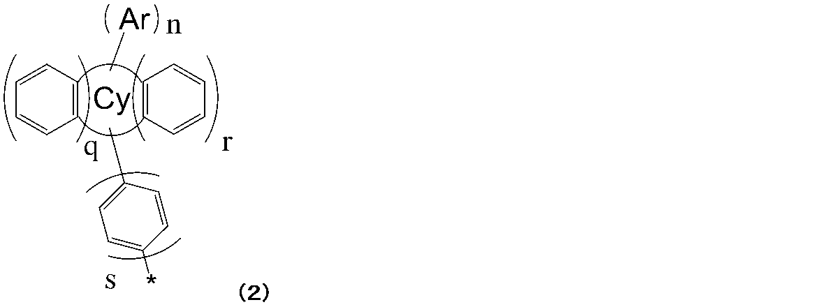
- B 1 is represented by the general formula (2).
- the Cy ring represents an aromatic 5-membered ring or 6-membered ring containing 1 to 3 nitrogen atoms and 0 to 1 oxygen atom.
- Q, r and s are each independently selected. 0 or 1, n is an integer of 0 to 2
- Ar is a phenyl group or biphenyl group which may have an alkyl group having 1 to 8 carbon atoms as a substituent, and * is in the general formula (1) represents the connection between L 1.
- n 1 to 1000
- R 1 and R 2 represent a hydrocarbon group which may have an ether bond
- R 3 represents a vinyl group or a vinyl group. Represents an organic group possessed).
- X 1 , X 2 and X 3 are each independently a carbon or nitrogen atom, Y 1 is a carbon or nitrogen atom, and Z 1 is nitrogen or Represents an oxygen atom.
- a composition comprising the polymer.
- An electronic material composition comprising the polymer.
- An electronic device comprising the composition or electronic material composition described above.
- the composition containing the novel heterocyclic ring-containing siloxane polymer of the present invention can produce a smooth organic thin film, and an electronic device obtained from these organic thin films has a luminous efficiency and a driving stability. We found that sex was improved.
- the heterocycle-containing siloxane polymer according to this embodiment is a copolymer obtained by copolymerizing at least one heterocycle-containing monomer represented by the general formula (1) and a siloxane monomer.
- the heterocycle-containing siloxane polymer may be a copolymer obtained by copolymerizing at least one heterocycle-containing monomer represented by the general formula (1), a siloxane monomer, and a monomer other than the general formula (1).
- the heterocyclic ring-containing siloxane polymer may contain components derived from the polymerization initiator.
- siloxane means a structure of “—Si—O—Si—” (siloxane structure).
- the siloxane monomer in the heterocyclic ring-containing siloxane polymer and other monomers including the heterocyclic monomer it is preferable to adjust the siloxane monomer in the heterocyclic ring-containing siloxane polymer and other monomers including the heterocyclic monomer.
- the silicon content in the heterocyclic ring-containing siloxane polymer is preferably 0.1% by mass or more, more preferably 0.1 to 80.0% by mass, and 3 to 80% by mass. %, More preferably 5 to 80% by mass. It is preferable that the silicon content in the heterocyclic ring-containing siloxane polymer is 0.1% by mass or more because surface energy can be reduced.
- the value of the silicon content can be controlled by appropriately adjusting the synthesis conditions of the polymer, for example, the addition amount of the siloxane monomer. In the present specification, the value calculated by the following formula is adopted as the value of “silicon content”.
- the heterocyclic monomer content in the heterocyclic ring containing siloxane polymer is 0.1 mol in consideration of the charge injection property to the light emitting layer. % Or more, preferably 0.1 to 99 mol%, more preferably 1 to 99 mol% or more. It is preferable that the heterocyclic monomer content in the heterocyclic ring-containing siloxane polymer be 0.1 mol% or more because charge injection into the light emitting layer can be improved. At this time, the content of the heterocyclic monomer can be controlled by appropriately adjusting the synthesis conditions of the polymer, for example, the addition amount of the heterocyclic monomer.
- the weight average molecular weight (Mw) of the heterocyclic ring-containing siloxane polymer is preferably 500 to 100,000, and more preferably 3,000 to 40,000.
- the weight-average molecular weight (Mw) of the heterocyclic ring-containing siloxane polymer is in the above range, the film thickness non-uniformity can be suppressed, and the electronic material should be made uniform particularly when used for forming an electronic material composition. It is preferable because it can be dissolved and dispersed.
- the value measured by the measuring method of an Example shall be employ
- the number average molecular weight (Mn) of the heterocyclic ring-containing siloxane polymer is preferably 500 to 100,000, more preferably 3,000 to 40,000.
- the film thickness non-uniformity can be suppressed, and particularly when used for forming an electronic material composition, the electronic material should be made uniform. It is preferable because it can be dissolved and dispersed.
- the value measured by the measuring method of an Example shall be employ
- Heterocycle-containing monomer The heterocyclic ring-containing monomer is represented by the following general formula (1).
- a 1 is a polymerizable reactive group
- L 1 is a single bond, a substituted or unsubstituted aromatic hydrocarbon group having 6 to 30 carbon atoms or a condensed aromatic hydrocarbon group.
- B 1 is represented by the general formula (2).
- the Cy ring represents an aromatic 5-membered ring or 6-membered ring containing 1 to 3 nitrogen atoms and 0 to 1 oxygen atom.
- Q, r and s are each independently selected. 0 or 1, n is an integer of 0 to 2
- Ar is a phenyl group or biphenyl group which may have an alkyl group having 1 to 8 carbon atoms as a substituent, and * is in the general formula (1) represents the connection between L 1.
- a 1 is preferably a methacryloxy group, an acryloxy group, a vinyl group, a vinyl group, or an organic group having a vinyl group, and is an organic group having a methacryloxy group, a vinyl group, or a vinyl group. More preferably.
- Examples of the organic group having a vinyl group include allyl group, 2-butenyl group, 3-butenyl group, 3-pentenyl group, 4-pentenyl group, 5-hexenyl group, butadienyl group, 2,4-pentadienyl group, 3,5 -Aliphatic hydrocarbon groups having vinyl groups such as hexadienyl group, 4,6-heptadienyl group, 5,7-octadienyl group; vinyloxymethylene group, vinyloxyethylene group, vinyloxypropylene group, vinyloxybutylene group, etc.
- an aliphatic hydrocarbon group having a vinyl group, a styryl group, and an aralkyl group having a vinyl group are preferable because of excellent polymerizability, and a vinyl group and a butadienyl group are easy to design a polymer having a wide molecular weight.
- An aralkyl group having a group, a pentadienyl group, a styryl group, or a vinyl group is particularly preferable.
- aromatic hydrocarbon group or condensed aromatic hydrocarbon group having 6 to 30 ring carbon atoms examples include phenyl group, naphthyl group, phenanthryl group, biphenyl group, terphenyl group, quarterphenyl group, fluoranthenyl group, triphenylenyl Group, phenanthrenyl group, pyrenyl group, chrycenyl group, fluorenyl group, and 9,9-dimethylfluorenyl group.
- an aromatic hydrocarbon group having 6 to 20 ring carbon atoms or a condensed aromatic hydrocarbon group is preferable.
- Cy ring pyrrolyl group, pyrazinyl group, pyridinyl group, indolyl group, isoindolyl group, furyl group, benzofuranyl group, isobenzofuranyl group, dibenzofuranyl group, dibenzothiophenyl group, quinolyl group, isoquinolyl group, quinoxalinyl Group, carbazolyl group, phenanthridinyl group, acridinyl group, phenanthrolinyl group, thienyl group, and pyridine ring, pyrazine ring, pyrimidine ring, pyridazine ring, triazine ring, indole ring, quinoline ring, acridine ring, pyrrolidine ring , Dioxane ring, piperidine ring, morpholine ring, piperazine ring, carbazole ring, furan ring, thiophen
- a pyridine ring, a pyrimidine ring, a triazine ring, a carbazole ring, an oxadiazole ring, a triazole ring, an imidazole ring, and a benzimidazole ring are preferable.
- heterocyclic ring-containing monomer represented by the general formula (1) include the following compounds.
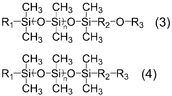
- siloxane monomer Although it does not restrict
- n 1 to 1000
- R 1 and R 2 represent a hydrocarbon group which may have an ether bond
- R 3 represents a methacryloxy group. Represents an acryloxy group, a vinyl group, or an organic group having a vinyl group.
- R 1 is not particularly limited, but is a C1-C10 alkyl group, a C2-C10 alkoxyalkyl group, a C3-C30 cycloalkyl group, a C4-C30 cycloalkoxyalkyl group, a C6-C20 aryl group, a C6-C20 aryl group.
- An oxy group is mentioned.
- the C1-C10 alkyl group is not particularly limited, but is methyl group, ethyl group, propyl group, isopropyl group, butyl group, iso-butyl group, sec-butyl group, tert-butyl group, pentyl group, hexyl group, decyl group. Groups and the like.
- the C2-C10 alkoxyalkyl group is not particularly limited, but is a methoxymethyl group, a methoxyethyl group, an ethoxyethyl group, a propoxyethyl group, a propoxypropyl group, a butoxypropyl group, a butoxybutyl group, a butoxypentyl group, a pentyloxypentyl group. Groups and the like.
- the C3-C30 cycloalkyl group is not particularly limited, but is a cyclopropyl group, a cyclobutyl group, a cyclopentyl group, a cyclohexyl group, a cycloheptyl group, a tricyclo [5,2,1,0 (2,6)] decyl group, And an adamantyl group.
- it is a group having 3 to 18 carbon atoms.
- the C4-C30 cycloalkoxyalkyl group is not particularly limited, but is a cyclopropyloxymethyl group, cyclobutyloxyethyl group, cyclopentyloxypropyl group, cyclohexyloxypropyl group, cycloheptyloxypropyl group, tricyclo [5,2, 1,0 (2,6)] decyloxypropyl group, adamantyloxypropyl group and the like.
- it is a group having 3 to 18 carbon atoms.
- Examples of the C6 to C20 aryl group include a phenyl group, a naphthyl group, an anthracenyl group, and a biphenyl group.
- Examples of the C6-C20 aryloxy group include a phenyloxy group, a naphthyloxy group, an anthracenyloxy group, and a biphenyloxy group.
- hydrogen constituting the C1 to C10 alkyl group, C1 to C10 alkoxyalkyl group, C3 to C30 cycloalkyl group, C3 to C30 cycloalkoxyalkyl group, C6 to C20 aryl group, and C6 to C20 aryloxy group At least one of the atoms may be substituted with a C1-C10 alkyl group as described above.
- R 1 is preferably a C1 to C10 alkyl group for improving leveling properties, and a methyl group, an ethyl group, a propyl group, an isopropyl group for enhancing compatibility with a solvent. More preferably a butyl group, an iso-butyl group, a sec-butyl group, or a tert-butyl group, and in order to improve electronic device characteristics, a methyl group, an ethyl group, a propyl group, or a butyl group. Further preferred.
- R 2 is not particularly limited, but is a C1-C10 alkylene group, a C2-C10 alkyleneoxyalkylene group, a C3-C30 cycloalkylene group, a C4-C30 cycloalkyleneoxyalkylene group, a C6-C20 arylene group, a C7-C20 Of the aryleneoxyalkylene group.
- the C1-C10 alkylene group is not particularly limited, and examples thereof include a methylene group, an ethylene group, a propylene group, an isopropylene group, a butylene group, an iso-butylene group, a pentylene group, a hexylene group, and a decylene group.
- the C2 to C10 alkyleneoxyalkylene group is not particularly limited, but a methyleneoxymethylene group, an ethyleneoxymethylene group, an ethyleneoxypropylene group, a propyleneoxyethylene group, a propyleneoxypropylene group, a propyleneoxybutylene group, a butyleneoxybutylene group. , Butyleneoxypentylene group, pentyleneoxypentylene group, and the like.
- the C3-C30 cycloalkylene group is not particularly limited, and examples thereof include a cyclopropylene group, a cyclobutylene group, a cyclopentylene group, a cyclohexylene group, and a cycloheptylene group. Preferably, it is a group having 3 to 10 carbon atoms.
- the C4-C30 cycloalkyleneoxyalkyl group is not particularly limited, but includes a cyclopropyleneoxyethylene group, a cyclobutyleneoxypropylene group, a cyclopentyleneoxypropylene group, a cyclohexyleneoxypropylene group, a cycloheptyleneoxypropylene group, and the like. Is mentioned. Preferably, it is a group having 3 to 10 carbon atoms.
- Examples of the C6 to C20 arylene group include a phenylene group, a naphthylene group, an anthracenylene group, and a biphenylene group.
- Examples of the C7 to C20 aryleneoxyalkylene group include a phenyleneoxypropylene group, a naphthyleneoxypropylene group, an anthracenyleneoxypropylene group, and a biphenyleneoxypropylene group.
- the C1 to C10 alkylene group, the C2 to C10 alkyleneoxyalkylene group, the C3 to C30 cycloalkylene group, the C4 to C30 cycloalkyleneoxyalkylene group, the C6 to C20 arylene group, and the C7 to C20 aryleneoxyalkylene group At least one of the constituent hydrogen atoms may be substituted with the above-described C1-C10 alkyl group.
- R 2 is preferably a C1 to C10 alkylene group or a C2 to C10 alkyleneoxyalkylene group in order to improve the leveling property, and a methylene group, an ethylene group, Propylene group, isopropylene group, butylene group, iso-butylene group, pentylene group, hexylene group, methyleneoxymethylene group, methyleneoxyethylene group, ethyleneoxyethylene group, ethyleneoxypropylene group, propyleneoxyethylene group, propyleneoxypropylene group , Propyleneoxybutylene group and butyleneoxybutylene group are particularly preferable.
- ethylene group, propylene group, butylene group, ethyleneoxyethylene group, ethyleneoxypropylene group, propyleneoxyethylene Down group and is more preferably propylene oxypropylene group.
- R 3 is a methacryloxy group, an acryloxy group, a vinyl group or an organic group having a vinyl group.
- Examples of the organic group having a vinyl group include allyl group, 2-butenyl group, 3-butenyl group, 3-pentenyl group, 4-pentenyl group, 5-hexenyl group, butadienyl group, 2,4-pentadienyl group, 3,5 -Aliphatic hydrocarbon groups having vinyl groups such as hexadienyl group, 4,6-heptadienyl group, 5,7-octadienyl group; vinyloxymethylene group, vinyloxyethylene group, vinyloxypropylene group, vinyloxybutylene group, etc.
- methacryloxy group, vinyl group, aliphatic hydrocarbon group having vinyl group, styryl group, and aralkyl group having vinyl group are preferable because of excellent polymerizability, and it is easy to design a polymer having a wide molecular weight.
- methacryloxy group, vinyl group, butadienyl group, pentadienyl group, styryl group, aralkyl group having a vinyl group is particularly preferable, since the resulting polymer improves the driving stability of the electronic device, vinyl group, More preferred are a butadienyl group, a 2,4-pentadienyl group, a styryl group, and a styrylmethylene group.
- n is 1 to 1000, and is preferably 3 to 500 because the smoothness of the coating film obtained from the electronic material composition / ink is excellent, and the driving stability of the electronic device is improved. Therefore, it is more preferably 5 to 200.
- siloxane monomer examples include siloxane monomer, but are not limited thereto.
- the monomers other than the general formula (1) are not particularly limited, and for example, known and commonly used (meth) acrylate monomers, styryl monomers, vinyl ether monomers, allyl monomers and the like can be used.
- the (meth) acrylate monomer is not particularly limited, but methyl (meth) acrylate, ethyl (meth) acrylate, propyl (meth) acrylate, (meth) acrylate-n-butyl, (meth) acrylic acid- t-butyl, hexyl (meth) acrylate, heptyl (meth) acrylate, octyl (meth) acrylate, nonyl (meth) acrylate, decyl (meth) acrylate, dodecyl (meth) acrylate, (meth) acrylic Alkyl (meth) acrylates such as tetradecyl acid, hexadecyl (meth) acrylate, octadecyl (meth) acrylate, docosyl (meth) acrylate; cyclohexyl (meth) acrylate, isobornyl (meth) acrylate, (met
- the styryl monomer is not particularly limited, and examples thereof include styrene; ⁇ -methylstyrene, ⁇ -ethylstyrene, ⁇ -butylstyrene, alkyl-substituted styrenes such as 4-methylstyrene, styrene such as chlorostyrene, and styrene derivatives. .
- the vinyl ether monomer is not particularly limited, but alkyl such as methyl vinyl ether, ethyl vinyl ether, propyl vinyl ether, isopropyl vinyl ether, n-butyl vinyl ether, sec-butyl vinyl ether, tert-butyl vinyl ether, isobutyl vinyl ether, n-amyl vinyl ether, isoamyl vinyl ether, etc.
- Vinyl ethers cyclopentyl vinyl ether, cyclohexyl vinyl ether, cycloheptyl vinyl ether, cyclooctyl vinyl ether, 2-bicyclo [2.2.1] heptyl vinyl ether, 2-bicyclo [2.2.2] octyl vinyl ether, 8-tricyclo [5.2 .1.0 (2,6)] decanyl vinyl ether, 1-adamantyl vinyl ether, 2-adamant Cycloalkyl vinyl ethers such as ruvinyl ether; aryl vinyl ethers such as phenyl vinyl ether, 4-methylphenyl vinyl ether, 4-trifluoromethylphenyl vinyl ether and 4-fluorophenyl vinyl ether; aryl vinyl ethers such as benzyl vinyl ether and 4-fluorobenzyl vinyl ether ; Etc.
- the allyl monomer is not particularly limited, but alkyl allyl ethers such as methyl allyl ether, ethyl allyl ether, propyl allyl ether, and butyl allyl ether; aryl allyl ethers such as phenyl allyl ether; allyl acetate, allyl alcohol, and allylamine Can be mentioned.
- these (meth) acrylate monomers, styryl monomers, vinyl ether monomers, and allyl monomers preferably contain a hydrophobic group.
- the “hydrophobic group” means a molecule having a water solubility (25 ° C., 25% RH) of a molecule formed by bonding a hydrophobic group with a hydrogen atom to 100 mg / L or less.
- the hydrophobic group is not particularly limited, and examples thereof include a C1-C18 alkyl group, a C3-C20 cycloalkyl group, and a C6-C30 aryl group.
- the C1-C18 alkyl group is not particularly limited, but is methyl group, ethyl group, propyl group, isopropyl group, butyl group, iso-butyl group, sec-butyl group, tert-butyl group, pentyl group, hexyl group, decyl group. Group, undecyl group, dodecyl group, octadecyl group, 2-ethylhexyl group and the like.
- the C3-C20 cycloalkyl group is not particularly limited, but is a cyclopropyl group, a cyclobutyl group, a cyclopentyl group, a cyclohexyl group, a cycloheptyl group, a tricyclo [5,2,1,0 (2,6)] decyl group, And an adamantyl group.
- Examples of the C6 to C30 aryl group include phenyl, naphthyl, anthracenyl, biphenyl and the like.
- Examples of the monomer having such a hydrophobic group include the above-described alkyl (meth) acrylates, cycloalkyl (meth) acrylates, aryl (meth) acrylates, styrene, alkyl-substituted styrenes, alkyls
- Examples thereof include vinyl ethers, cycloalkyl vinyl ethers, aryl vinyl ethers, alkyl allyl ethers, and aryl allyl ethers.
- the above-mentioned alkyl (meth) acrylate ester has good copolymerizability with the monomer represented by the general formula (1), and a polymer having a wide molecular weight can be obtained.
- Cycloalkyl (meth) acrylic acid esters, aryl (meth) acrylic acid esters, styrene, alkyl-substituted styrenes, alkyl vinyl ethers, cycloalkyl vinyl ethers, and aryl vinyl ethers are preferred.
- an aromatic-containing monomer containing an aryl group such as aryl (meth) acrylates, styrene, alkyl-substituted styrenes, aryl vinyl ethers, etc.
- aryl (meth) acrylates styrene, alkyl-substituted styrenes, aryl vinyl ethers, etc.
- styrene, alkyl-substituted styrenes, and aryl vinyl ethers are more preferable, and this is particularly true in the case of styrene, alkyl-substituted styrenes, phenyl vinyl ether, and benzyl vinyl ether.
- the effect of the invention is remarkable.
- the weight average molecular weight (Mw) of the polymer of the present invention is preferably 500 to 100,000, and more preferably 3,000 to 40,000 from the viewpoint of smoothness.
- the value measured by the measuring method of an Example shall be employ
- the number average molecular weight (Mn) of the polymer of the present invention is preferably 500 to 100,000, and more preferably 3,000 to 40,000 from the viewpoint of smoothness.
- the value measured by the measuring method of an Example shall be employ
- polymerization may be performed by a known and conventional method using the above-described monomer and polymerization initiator, and a random copolymer, block copolymer, graft copolymer may be used. Any of coalescence etc. may be sufficient.
- Examples of the polymerization method include radical polymerization, anionic polymerization, and cationic polymerization.
- the reaction conditions are not particularly limited.
- polymerization can be performed in a solvent using a monomer and a radical polymerization initiator.
- radical polymerization initiators such as 2,2′-azobisisobutyronitrile, 2,2′-azobis- (2,4-dimethylvaleronitrile), 2,2′-.
- Azo compounds such as azobis- (4-methoxy-2,4-dimethylvaleronitrile); benzoyl peroxide, lauroyl peroxide, t-butylperoxypivalate, t-butylperoxyethylhexanoate, 1,1'-bis- Examples thereof include organic peroxides such as (t-butylperoxy) cyclohexane, t-amylperoxy-2-ethylhexanoate, and t-hexylperoxy-2-ethylhexanoate, and hydrogen peroxide. These may be used alone or in combination of two or more.
- the amount of radical polymerization initiator used is not particularly limited, and is generally 0.001 to 1 part by mass with respect to 100 parts by mass of the monomer.
- the amount of the radical polymerization initiator used is preferably 0.005 to 0.5 parts by mass with respect to 100 parts by mass of the monomer. More preferably, the content is 0.01 to 0.3 parts by mass.
- Typical solvents that can be used for radical polymerization include, for example, acetone, methyl ethyl ketone, methyl-n-propyl ketone, methyl isopropyl ketone, methyl-n-butyl ketone, methyl isobutyl ketone, methyl-n-amyl ketone, Ketone solvents such as methyl-n-hexyl ketone, diethyl ketone, ethyl-n-butyl ketone, di-n-propyl ketone, diisobutyl ketone, cyclohexanone, holon; ethyl ether, isopropyl ether, n-butyl ether, diisoamyl ether, ethylene Ether solvents such as glycol dimethyl ether, ethylene glycol diethyl ether, diethylene glycol dimethyl ether, diethylene glycol, dioxane, tetrahydrofuran
- solvents may be used alone or in combination of two or more.
- the amount of the solvent used in the radical polymerization reaction is not particularly limited, but is preferably 0 to 3000 parts by mass with respect to 100 parts by mass of the monomer charged, from the viewpoint of agitation, and 10% from the viewpoint of reactivity. It is more preferably from 1000 parts by mass, and further preferably from 10 to 500 parts by mass from the viewpoint of molecular weight control.
- the reaction conditions are not particularly limited.
- polymerization can be performed in a solvent using a monomer and an anionic polymerization initiator.
- anionic polymerization initiators can be used, such as methyl lithium, n-butyl lithium, sec-butyl lithium, t-butyl lithium, isopropyl lithium, n-propyl lithium, isopropyl lithium phenyl lithium, benzyl
- Organic alkali metals such as lithium, hexyl lithium, butyl sodium and butyl potassium; organics such as methyl magnesium chloride, methyl magnesium bromide, methyl magnesium iodide, ethyl magnesium bromide, propyl magnesium bromide, phenyl magnesium chloride, phenyl magnesium bromide and dibutyl magnesium Alkaline earth metals; alkaline metals such as lithium, sodium, potassium; diethyl zinc, dibutyl zinc, ethyl butyl zinc, etc.
- Machine zinc trimethylaluminum, triethylaluminum, methylbisphenoxyaluminum, isopropylbisphenoxyaluminum, bis (2,6-di-t-butylphenoxy) methylaluminum, bis (2,6-di-t-butyl-4-methyl) And organic aluminum such as phenoxy) methylaluminum. These may be used alone or in combination of two or more.
- the amount of the anionic polymerization initiator used is not particularly limited, but is preferably 0.001 to 1 part by mass, and preferably 0.005 to 0.5 part by mass with respect to 100 parts by mass of the monomer. More preferred is 0.01 to 0.3 part by mass.
- solvent that can be used for anionic polymerization examples include those mentioned above.
- the amount of the solvent used in the anionic polymerization reaction is not particularly limited, but it is preferably 0 to 3000 parts by mass with respect to 100 parts by mass of the monomer charged from the viewpoint of agitation, and 10% from the viewpoint of reactivity. It is more preferably from 1000 parts by mass, and further preferably from 10 to 500 parts by mass from the viewpoint of molecular weight control.
- the reaction conditions are not particularly limited.
- polymerization can be performed in a solvent using a monomer and a cationic polymerization initiator.
- cationic polymerization initiators can be used, for example, protonic acids such as hydrochloric acid, sulfuric acid, perchloric acid, trifluoroacetic acid, methanesulfonic acid, trifluoromethanesulfonic acid, chlorosulfonic acid, and fluorosulfonic acid.
- protonic acids such as hydrochloric acid, sulfuric acid, perchloric acid, trifluoroacetic acid, methanesulfonic acid, trifluoromethanesulfonic acid, chlorosulfonic acid, and fluorosulfonic acid.
- Lewis acids such as boron trifluoride, aluminum chloride, titanium tetrachloride, stannic chloride, and ferric chloride. These may be used alone or in combination of two or more.
- the amount of the cationic polymerization initiator used is not particularly limited, and is generally 0.001 to 1 part by mass with respect to 100 parts by mass of the monomer.
- the amount of the cationic polymerization initiator used is preferably 0.005 to 0.5 parts by mass with respect to 100 parts by mass of the monomer. More preferably, the content is 0.01 to 0.3 parts by mass.
- Examples of the solvent that can be used for cationic polymerization include the solvents that can be used for the above-mentioned radical polymerization.
- the amount of the solvent used in the cationic polymerization reaction is not particularly limited, but is preferably 0 to 3000 parts by mass with respect to 100 parts by mass of the monomer charged from the viewpoint of stirring, and 10% from the viewpoint of reactivity.
- the amount is more preferably from 5 to 51,000 parts by mass, and further preferably from 10 to 500 parts by mass from the viewpoint of controlling the molecular weight.
- the radical polymerization, anionic polymerization, and cationic polymerization described above may be living polymerization.
- a method described in “Quarterly Chemical Review No. 18, 1993 Precision Polymerization, The Chemical Society of Japan (Academic Publishing Center)” may be used. it can.
- composition Since the composition containing the polymer of the present invention has a function of improving leveling properties after film formation, examples thereof include a curing composition by heat and light, an ink composition, a coating composition, and an electronic material composition. However, it is not limited to these. Among these, the polymer of the present invention is useful for an electronic material composition because it does not deteriorate the electrical characteristics of the electronic device.
- the electronic material composition containing the polymer of the present invention includes an organic semiconductor material, the polymer (leveling agent) of the present invention, and a solvent.
- the electronic material composition may contain a surfactant or the like as necessary.
- the content of the organic semiconductor material is preferably 0.01 to 10% by mass with respect to the total amount of the electronic material composition, and more preferably 0.01 to 5% by mass from the viewpoint of electrical characteristics.
- the content of the polymer of the present invention is preferably 0.001 to 5.0 mass% with respect to the total amount of the electronic material composition, and is 0.001 to 1.0 mass% from the viewpoint of leveling properties. More preferably.
- the content of the solvent is preferably 90 to 99% by mass with respect to the total amount of the electronic material composition, and more preferably 95 to 99% by mass from the viewpoint of film formability.
- Organic semiconductor materials examples include, but are not limited to, organic TFT materials, organic solar cell materials, and organic EL materials.
- the organic TFT material is not particularly limited as long as it is a material used for a layer constituting the organic TFT element.
- acenes having a substituent such as naphthalene, anthracene, tetracene, pentacene, hexacene, heptacene, etc.
- Nodimethane (TCNQ), quinoid oligomers such as 11,11,12,12-tetracyanonaphth-2,6-quinodimethane (TCNNQ), fullerenes such as C60, C70, PCBM, N, N′-diphenyl-3,4 , 9,10-perylenetetracarboxylic acid diimide, N, N′-dioctyl-3,4,9,10-perylenetetracarboxylic acid diimide (C8-PTCDI), NTCDA, 1,4,5,8-naphthalenetetracarboxyl And tetracarboxylic acids such as diimide (NTCDI).
- the organic solar cell material is not particularly limited as long as it is a material used for a layer constituting the organic solar cell element.
- Examples of the polymer system include CN-poly (phenylene-vinylene), MEH-CN-PPV, -CN group or CF3 group-containing polymer, -CF3 substituted polymer, poly (fluorene) derivative, and the like.
- the organic EL material is not particularly limited as long as it is a material used for a layer constituting the organic EL element.
- the organic EL material that can be contained in the electronic material composition includes a light emitting material used for a light emitting layer, a hole injection material used for a hole injection layer, and a positive electrode used for a hole transport layer. Examples thereof include a hole transport material and an electron transport material used for an electron transport layer.
- the light emitting material includes a host material and a dopant material.
- composition ratio of the host material and the dopant material is not limited to this, but the dopant is preferably 1 to 50 parts by weight with respect to 100 parts by weight of the host, and 5 to 20 parts by weight from the viewpoint of luminous efficiency. Further preferred.
- the host material is classified into a polymer host material and a low molecular host material.
- low molecule means that having a weight average molecular weight (Mw) of 5,000 or less.
- polymer means a polymer having a weight average molecular weight (Mw) of more than 5,000.
- weight average molecular weight (Mw) employs a value measured by gel permeation chromatography (GPC) using polystyrene as a standard substance.
- the polymer host material is not particularly limited, and examples thereof include poly (9-vinylcarbazole) (PVK), polyfluorene (PF), polyphenylene vinylene (PPV), and copolymers containing these monomer units.
- PVK poly (9-vinylcarbazole)
- PF polyfluorene
- PPV polyphenylene vinylene
- the weight average molecular weight (Mw) of the polymer host material is preferably more than 5,000 and less than 5,000,000, and from the viewpoint of film formability, it is more than 5,000 and less than 1,000,000. More preferred.
- the low molecular weight host material is not particularly limited, but 4,4′-bis (9H-carbazol-9-yl) biphenyl (CBP), 4,4′-bis (9-carbazolyl) -2,2′-dimethyl Biphenyl (CDBP), N, N′-dicarbazolyl-1,4-dimethylbenzene (DCB), 1,3-dicarbazolylbenzene (mCP), 3,5-bis (9-carbazolyl) tetraphenylsilane (SimCP ), 9,9 ′-(p-tert-butylphenyl) -1,3-biscarbazole, carbazole derivatives, 4,4′-di (di (triphenylsilyl) -biphenyl (BSB), 9- (4 -tert-butylphenyl) -3,6-bis (triphenylsilyl) -9H-carbazole (CzSi), 1,3-bis (triphenylsilyl
- the weight average molecular weight (Mw) of the low molecular weight host material is preferably 100 to 5,000, and more preferably 300 to 5,000 from the viewpoint of film formability.
- a low molecular weight host material is preferably used as the host material, and 4,4′-bis (9H-carbazol-9-yl) biphenyl (CBP), 9,9 ′-(p— carbazole derivatives such as tert-butylphenyl) -1,3-biscarbazole, bis (2-methyl-8-quinolinolate) -4- (phenylphenolato) aluminum (BAlq), oxadiazole derivatives, imidazole derivatives, triazine derivatives It is more preferable to use heterocyclic compounds such as pyridine derivatives and pyrimidine derivatives, and 4,4′-bis (9H-carbazol-9-yl) biphenyl (CBP), 9,9 ′-(p-tert-butylphenyl) ) -1,3-biscarbazole, imidazole derivatives, triazine derivatives, pyridine derivatives Body, it is more preferable to use a heterocyclic compound such
- the above host materials may be used alone or in combination of two or more.
- the dopant material is usually classified into a high molecular dopant material and a low molecular dopant material.
- the polymer dopant material is not particularly limited, but polyphenylene vinylene (PPV), cyano polyphenylene vinylene (CN-PPV), poly (fluorenylene ethynylene) (PFE), polyfluorene (PFO), polythiophene polymer, polypyridine, And copolymers containing these monomer units.
- the weight average molecular weight (Mw) of the polymer dopant material is preferably more than 5,000 and less than 5,000,000, and more preferably more than 5,000 and less than 1,000,000 from the viewpoint of light emission efficiency. preferable.
- the low molecular dopant material is not particularly limited, and examples thereof include fluorescent materials and phosphorescent materials.
- fluorescent light-emitting material examples include naphthalene, perylene, pyrene, chrysene, anthracene, coumarin, p-bis (2-phenylethenyl) benzene, quinacridone, coumarin, aluminum complexes such as Al (C 9 H 6 NO) 3, etc.
- rubrene perimidone, dicyanomethylene-2-methyl-6- (p-dimethylaminostyryl) -4H-pyran (DCM), benzopyran, rhodamine, benzothioxanthene, azabenzothioxanthene, and derivatives thereof. .
- Examples of the phosphorescent material include a complex containing a central metal of Groups 7 to 11 of the periodic table and an aromatic ligand coordinated to the central metal.
- Examples of the central metal of Group 7 to Group 11 of the periodic table include ruthenium, rhodium, palladium, osmium, iridium, gold, platinum, silver, and copper. Among these, from the viewpoint of luminous efficiency, the central metal is preferably iridium.
- the ligand examples include phenylpyridine, p-tolylpyridine, thienylpyridine, difluorophenylpyridine, phenylisoquinoline, fluorenopyridine, fluorenoquinoline, acetylacetone, and derivatives thereof.
- the ligand is preferably phenylpyridine, p-tolylpyridine, and derivatives thereof, and more preferably p-tolylpyridine and derivatives thereof from the viewpoint of film formability.
- Specific phosphorescent materials include tris (2-phenylpyridine) iridium (Ir (ppy) 3 ), tris (2-phenylpyridine) ruthenium, tris (2-phenylpyridine) palladium, bis (2-phenylpyridine) Platinum, tris (2-phenylpyridine) osmium, tris (2-phenylpyridine) rhenium, tris [2- (p-tolyl) pyridine] iridium (Ir (mppy) 3 ), tris [2- (p-tolyl) pyridine ] Ruthenium, tris [2- (p-tolyl) pyridine] palladium, tris [2- (p-tolyl) pyridine] platinum, tris [2- (p-tolyl) pyridine] osmium, tris [2- (p-tolyl) ) Pyridine] rhenium, octaethylplatinum porphyrin, octaphenyl
- the dopant material is preferably a low molecular dopant material, and is preferably a phosphorescent material from the viewpoint of luminous efficiency.
- the weight average molecular weight (Mw) of the low molecular dopant material is preferably 100 to 5,000, and more preferably 100 to 3,000.
- the above dopant materials may be used alone or in combination of two or more.
- a low molecular light emitting material is preferably used, and a low molecular host material and a low molecular dopant material are more preferably used from the viewpoint that higher luminous efficiency can be obtained.
- the hole injection material is not particularly limited, but is a phthalocyanine compound such as copper phthalocyanine; a triphenylamine derivative such as 4,4 ′, 4 ′′ -tris [phenyl (m-tolyl) amino] triphenylamine; , 5,8,9,12-hexaazatriphenylenehexacarbonitrile, 2,3,5,6-tetrafluoro-7,7,8,8-tetracyano-quinodimethane and other cyano compounds; vanadium oxide, molybdenum oxide, etc.
- a phthalocyanine compound such as copper phthalocyanine
- a triphenylamine derivative such as 4,4 ′, 4 ′′ -tris [phenyl (m-tolyl) amino] triphenylamine
- 5,8,9,12-hexaazatriphenylenehexacarbonitrile 2,3,5,6-tetrafluoro-7,7,8,8-tetracyano-quinodimethane and
- the hole injecting material is preferably a polymer from the viewpoint of film formability.
- the above hole injection materials may be used alone or in combination of two or more.
- the hole transport material is not particularly limited, but includes TPD (N, N′-diphenyl-N, N′-di (3-methylphenyl) -1,1′-biphenyl-4,4′diamine), ⁇ - NPD (4,4′-bis [N- (1-naphthyl) -N-phenylamino] biphenyl), m-MTDATA (4,4 ′, 4 ′′ -tris (3-methylphenylphenylamino) triphenylamine)
- a low molecular weight triphenylamine derivative such as polyvinylcarbazole, a polymer compound obtained by polymerizing a triphenylamine derivative represented by the following chemical formula HT-2 by introducing a substituent, etc.
- a hole transport material Is a high molecular compound such as HT-2 represented by Formula 5 in which a substituent is introduced into a triphenylamine derivative or a triphenylamine derivative from the viewpoint of hole transportability. Preferred.
- the above hole transport materials may be used alone or in combination of two or more.
- the electron transport material is not particularly limited, but tris (8-quinolylato) aluminum (Alq), tris (4-methyl-8-quinolinolato) aluminum (Almq3), bis (10-hydroxybenzo [h] quinolinato) beryllium ( A metal complex having a quinoline skeleton or a benzoquinoline skeleton such as BeBq2), bis (2-methyl-8-quinolinolato) (p-phenylphenolate) aluminum (BAlq), bis (8-quinolinolato) zinc (Znq); 2- (2′-hydroxyphenyl) benzoxazolate] zinc (Zn (BOX) 2) and other metal complexes having a benzoxazoline skeleton; bis [2- (2′-hydroxyphenyl) benzothiazolate] zinc ( Zn (BTZ) 2) Metal complex having benzothiazoline skeleton 2- (4-biphenylyl) -5- (4-tert-butylphenyl) -1,3,4
- Benzimidazole derivatives such as ET-1 represented by Chemical Formula 6; quinoline derivatives; perylene derivatives; pyridine derivatives; pyrimidine derivatives; triazine derivatives; quinoxaline derivatives; diphenylquinone derivatives; nitro-substituted fluorene derivatives.
- the electron transport material is preferably a benzimidazole derivative, a pyridine derivative, a pyrimidine derivative, or a triazine derivative from the viewpoint of electron transport properties.
- the above electron transport materials may be used alone or in combination of two or more.
- solvent is not particularly limited, and known solvents can be used as appropriate. Specific examples include aromatic solvents, alkane solvents, ether solvents, alcohol solvents, ester solvents, amide solvents, other solvents, and the like.
- aromatic solvent examples include toluene, xylene, ethylbenzene, cumene, pentylbenzene, hexylbenzene, cyclohexylbenzene, dodecylbenzene, mesitylene, diphenylmethane, dimethoxybenzene, phenetole, methoxytoluene, anisole, methylanisole, and dimethylanisole.
- Cyclic aromatic solvents condensed cyclic aromatic solvents such as cyclohexylbenzene, tetralin, naphthalene, and methylnaphthalene; ether-based aromatic solvents such as methylphenyl ether, ethylphenyl ether, propylphenyl ether, and butylphenyl ether; phenyl acetate; And ester aromatic solvents such as phenyl propionate, ethyl benzoate, propyl benzoate, and butyl benzoate.
- alkane solvent examples include pentane, hexane, octane, and cyclohexane.
- ether solvent examples include dioxane, ethylene glycol dimethyl ether, ethylene glycol diethyl ether, propylene glycol-1-monomethyl ether acetate, tetrahydrofuran and the like.
- Examples of the alcohol solvent include methanol, ethanol, isopropyl alcohol and the like.
- ester solvent examples include ethyl acetate, butyl acetate, ethyl lactate, and butyl lactate.
- amide solvent examples include N, N-dimethylformamide, N, N-dimethylacetamide and the like.
- Examples of the other solvent include water, dimethyl sulfoxide, acetone, chloroform, methylene chloride and the like.
- the solvent is preferably an aromatic solvent from the viewpoint of solubility of the organic semiconductor material, and from the viewpoint of leveling properties, a condensed cyclic aromatic solvent, an ether aromatic solvent, and an ester solvent. It is more preferable to include at least one selected from the group consisting of aromatic solvents, and from the viewpoint of film formability, it is more preferable to use a condensed cyclic aromatic solvent and / or an ether-based aromatic solvent.
- the above-mentioned solvent may be used independently or may be used in combination of 2 or more type.
- the polymer of the present invention which becomes a leveling agent, has a siloxane structure and is thus oriented on the coating film surface to reduce the surface tension. Then, by drying the coating film obtained in such a state, it is possible to prevent the occurrence of waviness due to drying, and to obtain a highly flat layer, and thus an organic functional layer having high performance. be able to.
- a function of improving the driving stability of the organic EL element can be exhibited.
- Such a function is considered to be a charge because the polymer of the present invention has a heterocyclic structure.
- the luminescent material includes a host material and a dopant material.
- the light emitting layer holes and / or electrons are transported by the host material, and the light emitting layer emits light by using energy generated by recombination of the holes and electrons transported by the dopant material. Therefore, if holes and electrons are efficiently transported in the light emitting layer, efficient light emission is possible and driving stability is improved.
- the leveling agent structure has a functional group that can inhibit electron injection, such as charge aralkyl group, polyether group, carbonyl group, etc., which deteriorates the charge balance in the light emitting layer and impairs the light emitting efficiency and driving stability of the device. Can be. That is, when a conventional leveling agent is used, the effect of preventing undulation can be obtained to a certain extent, but at the cost of light emission efficiency and driving stability can be reduced.
- the leveling agent contains a heterocyclic ring
- the electron injection barrier is lowered as compared with the conventional leveling, so that inhibition of charge transport can be suppressed.
- charges are efficiently transported in the light emitting layer, and the light emission efficiency and driving stability of the device can be improved.
- An electronic device containing a composition or an electronic material composition containing the polymer of the present invention in any form includes photoelectric conversion elements such as solar cells and light receiving elements, transistors such as field effect transistors, electrostatic induction transistors and bipolar transistors, organic electroluminescence elements (hereinafter abbreviated as organic EL elements), Examples include, but are not limited to, temperature sensors, gas sensors, humidity sensors, and radiation sensors.
- photoelectric conversion elements such as solar cells and light receiving elements
- transistors such as field effect transistors, electrostatic induction transistors and bipolar transistors
- organic EL elements organic electroluminescence elements
- Examples include, but are not limited to, temperature sensors, gas sensors, humidity sensors, and radiation sensors.
- an organic EL element will be described below.
- the organic EL element containing an anode, a light emitting layer, and a cathode is provided.
- the light emitting layer is formed of an electronic material composition.
- the organic EL element may include one or more other layers such as a hole injection layer, a hole transport layer, an electron transport layer, and an electron injection layer. Moreover, you may include well-known things, such as a sealing member.
- An organic EL device is provided.
- at least one layer selected from the group consisting of a light emitting layer, a hole injection layer, a hole transport layer, and an electron transport layer contains the polymer (leveling agent) of the present invention.
- the organic EL element has at least one selected from the group consisting of a hole injection layer, a hole transport layer, an electron transport layer, and an electron injection layer, with the anode, the light emitting layer, and the cathode as minimum structural units.
- a layer may be included as an arbitrary structural unit.
- the leveling agent may be contained only in the light emitting layer, or only in at least one layer selected from the group consisting of a hole injection layer, a hole transport layer, and an electron transport property (for example, a positive layer).
- Hole transport layer only, hole transport layer and electron transport layer) or light emitting layer and at least one of the hole injection layer, hole transport layer and electron transport layer. May be.
- it is preferable that a light emitting layer and / or a hole transport layer contain a leveling agent, and it is more preferable that a light emitting layer contains a leveling agent.
- the anode is not particularly limited, and metals such as gold (Au), copper iodide (CuI), indium tin oxide (ITO), tin oxide (SnO 2 ), zinc oxide (ZnO), and the like can be used. These materials may be used alone or in combination of two or more.
- the film thickness of the anode is not particularly limited, but is preferably 10 to 1000 nm, and more preferably 10 to 200 nm.
- the anode can be formed by a method such as vapor deposition or sputtering. At this time, pattern formation may be performed by a photolithography method or a method using a mask.
- the hole injection layer is an optional component in the organic light emitting device and has a function of taking holes from the anode. Normally, holes taken from the anode are transported to the hole transport layer or the light emitting layer.
- the thickness of the hole injection layer is not particularly limited, but is preferably 0.1 nm to 5 ⁇ m.
- the hole injection layer may be a single layer or a laminate of two or more.
- the hole injection layer can be formed by a wet film forming method and a dry film forming method.
- the hole injection layer When the hole injection layer is formed by a wet film formation method, it usually includes a step of applying the above-described ink composition for an organic light-emitting device and drying the obtained coating film.
- the application method is not particularly limited, and examples thereof include an ink jet printing method, a relief printing method, a gravure printing method, a screen printing method, and a nozzle printing method.
- the hole injection layer is formed by a dry film forming method, a vacuum deposition method, a spin coating method, or the like can be applied.
- the hole transport layer is an optional component in the organic light emitting device and has a function of efficiently transporting holes.
- the hole transport layer may have a function of preventing hole transport.
- the hole transport layer usually takes holes from the anode or the hole injection layer and transports the holes to the light emitting layer.
- the film thickness of the hole transport layer is not particularly limited, but is preferably 1 nm to 5 ⁇ m, more preferably 5 nm to 1 ⁇ m, and further preferably 10 to 500 nm.
- the hole transport layer may be a single layer or a laminate of two or more.
- the hole transport layer can be formed by a wet film formation method and a dry film formation method.
- the hole transport layer is formed by a wet film forming method
- it usually includes a step of applying the above-described ink composition for an organic light emitting device and drying the obtained coating film.
- the application method is not particularly limited, and examples thereof include an ink jet printing method, a relief printing method, a gravure printing method, a screen printing method, and a nozzle printing method.
- the hole transport layer is formed by a dry film forming method, a vacuum deposition method, a spin coating method, or the like can be applied.
- the light emitting layer has a function of causing light emission by using energy generated by recombination of holes and electrons injected into the light emitting layer.
- the thickness of the light emitting layer is not particularly limited, but is preferably 2 to 100 nm, and more preferably 2 to 20 nm.
- the light emitting layer can be formed by a wet film forming method and a dry film forming method.
- the light emitting layer When the light emitting layer is formed by a wet film forming method, it usually includes a step of applying the above-described ink composition for an organic light emitting device and drying the obtained coating film.
- the application method is not particularly limited, and examples thereof include an ink jet printing method, a relief printing method, a gravure printing method, a screen printing method, and a nozzle printing method.
- the light emitting layer is formed by a dry film forming method, a vacuum deposition method, a spin coating method, or the like can be applied.
- the electron transport layer is an optional component in the organic light emitting device and has a function of efficiently transporting electrons.
- the electron transport layer can have a function of preventing electron transport.
- the electron transport layer usually takes electrons from the cathode or the electron injection layer and transports the electrons to the light emitting layer.
- the thickness of the electron transport layer is not particularly limited, but is preferably 5 nm to 5 ⁇ m, and more preferably 5 to 200 nm.
- the electron transport layer may be a single layer or a laminate of two or more.
- the electron transport layer can be formed by a wet film formation method and a dry film formation method.
- the electron transport layer When the electron transport layer is formed by a wet film formation method, it usually includes a step of applying the above-described ink composition for an organic light emitting device and drying the obtained coating film.
- the application method is not particularly limited, and examples thereof include an ink jet printing method, a relief printing method, a gravure printing method, a screen printing method, and a nozzle printing method.
- the electron transport layer is formed by a dry film forming method, a vacuum deposition method, a spin coating method, or the like can be applied.
- the electron injection layer is an optional component in the organic light emitting device and has a function of taking electrons from the cathode. Usually, electrons taken from the cathode are transported to the electron transport layer or the light emitting layer.
- the electron injection material is not particularly limited, but alkali metals such as lithium and calcium; metals such as strontium and aluminum; alkali metal salts such as lithium fluoride and sodium fluoride; alkali metal compounds such as 8-hydroxyquinolate lithium An alkaline earth metal salt such as magnesium fluoride; an oxide such as aluminum oxide; Among these, the electron injecting material is preferably an alkali metal, an alkali metal salt, or an alkali metal compound, and more preferably an alkali metal salt or an alkali metal compound.
- the above-described electron injection materials may be used alone or in combination of two or more.
- the thickness of the electron injection layer is not particularly limited, but is preferably 0.1 nm to 5 ⁇ m.
- the electron injection layer may be a single layer or a laminate of two or more.
- the electron injection layer can be formed by a wet film forming method and a dry film forming method.
- the electron injection layer When the electron injection layer is formed by a wet film formation method, it usually includes a step of applying the above-described ink composition for an organic light emitting device and drying the obtained coating film.
- the application method is not particularly limited, and examples thereof include an ink jet printing method, a relief printing method, a gravure printing method, a screen printing method, and a nozzle printing method.
- the electron injection layer is formed by a dry film forming method, a vacuum deposition method, a spin coating method, or the like can be applied.
- cathode examples include, but are not limited to, lithium, sodium, magnesium, aluminum, sodium-potassium alloy, magnesium / aluminum mixture, magnesium / indium mixture, aluminum / aluminum oxide (Al 2 O 3 ) mixture, rare earth metal, and the like. . These materials may be used alone or in combination of two or more.
- the cathode can be usually formed by a method such as vapor deposition or sputtering.
- the film thickness of the cathode is not particularly limited, but is preferably 10 to 1000 nm, and more preferably 10 to 200 nm.
- an organic EL element including a layer formed using the electronic material composition described above can suitably prevent non-uniform film thickness of the formed layer. Thereby, the obtained organic EL element has high performance, such as a variation in luminance.
- the obtained organic EL device can realize excellent light emission efficiency and driving stability.
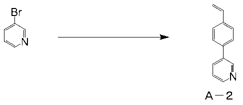
- a heterocycle-containing monomer A-2 (0.81 g, 44%) was obtained in the same manner as in Synthesis Example 1 except that 2-bromopyridine was changed to 3-bromopyridine.
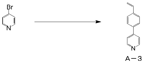
- Heterocycle-containing monomer A-3 (0.8 g, 43%) was obtained in the same manner as in Synthesis Example 1, except that 2-bromopyridine was changed to 3-bromopyridine.
- a heterocycle-containing monomer A-6 was prepared in the same manner as in Synthesis Example 5 except that 2- (4-bromophenyl) -1-phenylbenzimidazole was changed to 1- (4-bromophenyl) -2-phenylbenzimidazole. (0.36 g, 30%) was obtained.
- Heterocycle-containing monomer A-7 (2.5 g, 46%) was obtained in the same manner as in Synthesis Example 1 except that 2-bromopyridine was changed to 1- (4-bromophenyl) -2-phenylbenzimidazole.
- Heterocycle-containing monomer A-12 (0.8 g, 9%) was obtained in the same manner as in Example 10 except that acetophenone was changed to 4'-hexyl acetophenone.
- Heterocycle-containing monomer A-13 (1.0 g, 12%) was obtained in the same manner as in Example 10 except that acetophenone was changed to 4'-tert-acetophenone.
- Heterocycle-containing monomer A-15 (3.0 g, 42%) was obtained in the same manner as in Example 10, except that M-4 was changed to M-6.
- Heterocycle-containing monomer A-16 (0.7 g, 19%) was obtained in the same manner as in Synthesis Example 14 except that benzonitrile was changed to 4-tert-butylbenzonitrile.
- Heterocycle-containing monomer A-17 (1.3 g, 41%) was obtained in the same manner as in Synthesis Example 10, except that M-4 was changed to M-7.
- siloxane monomer B-1 The structure of siloxane monomer B-1 is shown below.
- Examples 30 to 33 Polymers P-30 to 33 were obtained in the same manner as in Example 20, except that 500 mg of the heterocyclic monomer was changed to 250 mg of the heterocyclic monomer and 250 mg of the third monomer.
- Table 1 shows the charged amount of each monomer and the number average molecular weight (Mn) and the weight average molecular weight (Mw) of the obtained polymers P1 to P31.
- Mn number average molecular weight
- Mw weight average molecular weight
- Example 34 0.001 g of the polymer P-1 synthesized in Example 1 was dissolved in 9.9 g of tetralin as a solvent. To the resulting solution, 0.04 g of tris [2- (p-tolyl) pyridine] iridium (Ir (mppy) 3 ) (manufactured by Lumtec) and 0.26 g of 9,9 ′ synthesized in Synthesis Example 20 were added. An electronic material composition was produced by adding-(p-tert-butylphenyl) -1,3-biscarbazole and heating at 60 ° C.
- Example 35 to 66 An electronic material composition was produced in the same manner as in Example 34, except that the polymer P-1 was changed to the polymers P-2 to 33 synthesized in Examples 1 to 33.
- the organic EL element was produced as follows.
- UV / O 3 was irradiated onto the cleaned ITO substrate, and a poly (3,4-ethylenedioxythiophene) -poly (styrenesulfonic acid) (PEDOT-PSS) film having a thickness of 45 nm was formed by spin coating.
- the hole injection layer was formed by heating at 180 ° C. for 15 minutes.
- a 0.3 wt% xylene solution of HT-2 represented by the following formula was formed on the hole injection layer by spin coating to a thickness of 10 nm and dried at 200 ° C. for 30 minutes in a nitrogen atmosphere.
- a hole transport layer was formed.
- the electronic material compositions obtained in Examples 34 to 66 and the comparative example were formed on the hole transport layer by spin coating, dried under reduced pressure at 25 ° C. and 1 Torr for 3 minutes, and then in a nitrogen atmosphere.
- a light emitting layer having a thickness of 30 nm was formed by drying at 110 ° C. for 15 minutes.
- 45 nm of ET-1 represented by the following formula is sequentially formed as an electron transport layer, 0.5 nm of lithium fluoride as an electron injection layer, and 100 nm of aluminum as a cathode. did.
- the substrate was transported to a glove box and sealed with a glass substrate to produce an organic light emitting device.
- Luminescence efficiency was evaluated using the produced organic EL element.
- the produced organic EL device was connected to an external power source, and light emission from the organic EL device was measured with BM-9 (manufactured by Topcon Corporation). At this time, the luminous efficiency at 10 mA / cm 2 was calculated from the current value.
Landscapes
- Chemical & Material Sciences (AREA)
- Organic Chemistry (AREA)
- Health & Medical Sciences (AREA)
- Chemical Kinetics & Catalysis (AREA)
- Medicinal Chemistry (AREA)
- Polymers & Plastics (AREA)
- Engineering & Computer Science (AREA)
- Materials Engineering (AREA)
- Electroluminescent Light Sources (AREA)
- Compositions Of Macromolecular Compounds (AREA)
- Addition Polymer Or Copolymer, Post-Treatments, Or Chemical Modifications (AREA)
Abstract
Description


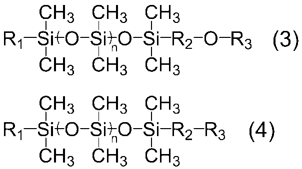
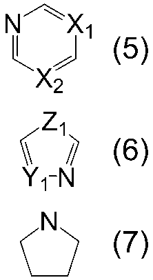
本形態に係る複素環含有シロキサン重合体は、一般式(1)で表される少なくとも1種の複素環含有モノマー、及びシロキサンモノマーを共重合させてなる共重合体である。前記複素環含有シロキサン重合体は、一般式(1)で表される少なくとも1種の複素環含有モノマー、シロキサンモノマー、及び一般式(1)以外のモノマーを共重合させてなる共重合体でもよい。この際、前記複素環含有シロキサン重合体は、重合開始剤に起因する成分等を含んでいてもよい。なお、本明細書において、「シロキサン」とは、「-Si-O-Si-」の構造(シロキサン構造)を意味する。

複素環含有モノマーは、下記一般式(1)で表される。


シロキサンモノマーが有するシロキサン基としては、特に制限されないが、下記式(3)または、下記式(4)で表されるものであることが好ましい。


一般式(1)以外のモノマーは、特に制限されることなく例えば、公知慣用の(メタ)アクリレートモノマー、スチリルモノマー、ビニルエーテルモノマー、アリルモノマー等を使用することができる。
本発明の重合体を得るには、上述のモノマーと重合開始剤とを用いて、公知慣用の方法で重合(共重合)させれば良く、ランダム共重合体、ブロック共重合体、グラフト共重合体等のいずれでもよい。
本発明の重合体を含有する組成物は、成膜後のレベリング性を向上する機能を有することから、熱や光による硬化組成物、インク組成物、コーティング組成物、電子材料組成物などが挙げられるが、これらに限定されるのもではない。なかでも、本発明の重合体は、電子素子の電気特性を低下させないことから電子材料組成物に有用である。
本発明の重合体を含有する電子材料組成物は、有機半導体材料、本発明の重合体(レベリング剤)、および溶媒を含む。なお、前記電子材料組成物には、その他、必要に応じて、界面活性剤等が含まれていてもよい。
有機半導体材料としては、有機TFT材料、有機太陽電池材料、有機EL材料などが挙げられるが、これらに限定されるものではない。
発光材料は、ホスト材料およびドーパント材料を含む。
正孔注入材料としては、特に制限されないが、銅フタロシアニン等のフタロシアニン化合物;4,4’,4”-トリス[フェニル(m-トリル)アミノ]トリフェニルアミン等のトリフェニルアミン誘導体;1,4,5,8,9,12-ヘキサアザトリフェニレンヘキサカルボニトリル、2,3,5,6-テトラフルオロ-7,7,8,8-テトラシアノ-キノジメタン等のシアノ化合物;酸化バナジウム、酸化モリブデン等の酸化物;アモルファスカーボン;ポリアニリン(エメラルディン)、ポリ(3,4-エチレンジオキシチオフェン)-ポリ(スチレンスルホン酸)(PEDOT-PSS)、ポリピロール等の高分子が挙げられる。これらのうち、正孔注入材料は、成膜性の観点から、高分子であることが好ましい。
正孔輸送材料としては、特に制限されないが、TPD(N,N'-ジフェニル-N,N’-ジ(3-メチルフェニル)-1,1’-ビフェニル-4,4’ジアミン)、α-NPD(4,4’-ビス[N-(1-ナフチル)-N-フェニルアミノ]ビフェニル)、m-MTDATA(4、4’,4”-トリス(3-メチルフェニルフェニルアミノ)トリフェニルアミン)等の低分子トリフェニルアミン誘導体;ポリビニルカルバゾール;下記化学式HT-2で表されるトリフェニルアミン誘導体に置換基を導入して重合した高分子化合物等が挙げられる。これらのうち、正孔輸送材料は、正孔輸送性の観点から、トリフェニルアミン誘導体、トリフェニルアミン誘導体に置換基を導入して重合した化5で表されるHT-2の如き高分子化合物であることが好ましい。

電子輸送材料としては、特に制限されないが、トリス(8-キノリラート)アルミニウム(Alq)、トリス(4-メチル-8-キノリノラート)アルミニウム(Almq3)、ビス(10-ヒドロキシベンゾ[h]キノリナート)ベリリウム(BeBq2)、ビス(2-メチル-8-キノリノラート)(p-フェニルフェノラート)アルミニウム(BAlq)、ビス(8-キノリノラート)亜鉛(Znq)等のキノリン骨格またはベンゾキノリン骨格を有する金属錯体;ビス[2-(2’-ヒドロキシフェニル)ベンズオキサゾラート]亜鉛(Zn(BOX)2)等のベンズオキサゾリン骨格を有する金属錯体;ビス[2-(2’-ヒドロキシフェニル)ベンゾチアゾラート]亜鉛(Zn(BTZ)2)ベンゾチアゾリン骨格を有する金属錯体;2-(4-ビフェニリル)-5-(4-tert-ブチルフェニル)-1,3,4-オキサジアゾール(PBD)、3-(4-ビフェニリル)-4-フェニル-5-(4-tert-ブチルフェニル)-1,2,4-トリアゾール(TAZ)、1,3-ビス[5-(p-tert-ブチルフェニル)-1,3,4-オキサジアゾール-2-イル]ベンゼン(OXD-7)、9-[4-(5-フェニル-1,3,4-オキサジアゾール-2-イル)フェニル]カルバゾール(CO11)、2,2’,2’’-(1,3,5-ベンゼントリイル)トリス(1-フェニル-1H-ベンゾイミダゾール)(TPBI)、2-[3-(ジベンゾチオフェン-4-イル)フェニル]-1-フェニル-1H-ベンゾイミダゾール(mDBTBIm-II)等のポリアゾール誘導体;化6で表されるET-1の如きベンゾイミダゾール誘導体;キノリン誘導体;ペリレン誘導体;ピリジン誘導体;ピリミジン誘導体;トリアジン誘導体;キノキサリン誘導体;ジフェニルキノン誘導体;ニトロ置換フルオレン誘導体等が挙げられる。これらのうち、電子輸送材料は、電子輸送性の観点から、ベンゾイミダゾール誘導体、ピリジン誘導体、ピリミジン誘導体、トリアジン誘導体であることが好ましい。

溶媒としては、特に制限されず、適宜公知のものが使用できる。具体的には、芳香族系溶媒、アルカン系溶媒、エーテル系溶媒、アルコール系溶媒、エステル系溶媒、アミド系溶媒、他の溶媒等が挙げられる。
次に、本発明の電子素子について説明する。本発明の重合体を含有する組成物または電子材料組成物をいかなる形態でも含有している電子素子である。電子素子の具体例として、太陽電池や受光素子などの光電変換素子、電界効果型トランジスタや静電誘導型トランジスタやバイポーラトランジスタ等のトランジスタ、有機エレクトロルミネッセンス素子(以下、有機EL素子と略する)、温度センサー、ガスセンサー、湿度センサー、放射線センサーなどが挙げられるが、これらに限定されるものではない。
本発明の一形態によれば、陽極、発光層、および陰極を含む有機EL素子が提供される。この際、前記発光層が、電子材料組成物から形成されることを特徴とする。
陽極としては、特に制限されないが、金(Au)等の金属、ヨウ化銅(CuI)、インジウムスズ酸化物(ITO)、酸化スズ(SnO2)、酸化亜鉛(ZnO)等が用いられうる。これらの材料は、単独で用いても、2種以上を組み合わせて用いてもよい。
正孔注入層は、有機発光素子において任意の構成要素であり、陽極から正孔を取り入れる機能を有する。通常、陽極から取り入れた正孔は、正孔輸送層または発光層に輸送される。
正孔輸送層は、有機発光素子において任意の構成要素であり、正孔を効率的に輸送する機能を有する。また、正孔輸送層は、正孔の輸送を防止する機能を有しうる。正孔輸送層は、通常、陽極または正孔注入層から正孔を取り入れ、発光層に正孔を輸送する。
発光層は、発光層に注入された正孔および電子の再結合により生じるエネルギーを利用して発光を生じさせる機能を有する。
電子輸送層は、有機発光素子において任意の構成要素であり、電子を効率的に輸送する機能を有する。また、電子輸送層は、電子の輸送を防止する機能を有しうる。電子輸送層は、通常、陰極または電子注入層から電子を取り入れ、発光層に電子を輸送する。
電子注入層は、有機発光素子において任意の構成要素であり、陰極から電子を取り入れる機能を有する。通常、陰極から取り入れた電子は、電子輸送層または発光層に輸送される。
陰極としては、特に制限されないが、リチウム、ナトリウム、マグネシウム、アルミニウム、ナトリウム-カリウム合金、マグネシウム/アルミニウム混合物、マグネシウム/インジウム混合物、アルミニウム/酸化アルミニウム(Al2O3)混合物、希土類金属等が挙げられる。これらの材料は、単独で用いても、2種以上を組み合わせて用いてもよい。
[合成例1](A-1の合成)
合成スキームを以下に示す。

合成スキームを以下に示す。
合成スキームを以下に示す。
合成スキームを以下に示す。

合成スキームを以下に示す。

乾燥窒素雰囲気下の脱水THF(35.0mL)に2-(4-ブロモフェニル)-1-フェニルベンゾイミダゾール (3.00g,8.59mmol)を加え、-78℃に冷却後、n-ブチルリチウム1.6MTHF溶液(6.4g,10.31mmol)を滴下した。2時間撹拌後、脱水DMF(4.0mL)を加え、25℃で1時間撹拌した。次いで、1時間還流後、室温まで冷却し、塩化アンモニウム水溶液及びジクロロメタンを加え、有機層を分離した。硫酸マグネシウムで有機層を乾燥後、有機溶媒を減圧下留去した。得られた残渣をシリカゲルクロマトグラフィーにて精製し、中間体モノマーM-1(1.18g,46%)を得た。
N-(4-ホルミルフェニル)カルバゾールをM-1(1.18g,3.95mmol)に変更した以外は、合成例4と同様にして、複素環含有モノマーA-6(0.45g,38%)を得た。
合成スキームを以下に示す。
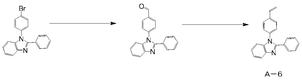
合成スキームを以下に示す。

合成スキームを以下に示す。

ピリジン(14mL)にベンゾイルクロライド(0.96g,4.88mmol)を加え、次いで、5-(4-ブロモフェニル)-1H-テトラゾール(1.0g,4.44mmol)を加えた。100℃で8時間撹拌後、常温まで冷却し、水を加えて析出物をろ過した。ろ過物をエタノールにて再結晶することで中間体モノマーM-2(0.8g,52%)を得た。
THF(10mL)に炭酸カリウム2M水溶液(2.0mL)を加え、窒素雰囲気下、M-2(0.8g,2.31mmol)、4-ビニルフェニルボロン酸(0.26g,1.76mmol)をさらに加えた。次いで、テトラキス(トリフェニルホスフィン)パラジウム(0)(9.5mg,8.2μmol)を加えて80℃で12時間撹拌した。反応液を室温まで冷却し、ジクロロメタン及び水を加え、有機層を分離し、硫酸マグネシウムで乾燥後、有機溶媒を減圧下留去した。得られた残渣をシリカゲルクロマトグラフィーにて精製し、複素環含有モノマーA-8(0.38g,43%)を得た。
合成スキームを以下に示す。

合成スキームを以下に示す。

4-ブロモベンズアルデヒド(25g,135mmol)、アセトフェノン(16.2g,135mmol)をエタノールに加え、さらに3M水酸化カリウム水溶液(60mL)を加えて室温で7時間撹拌した。析出した固体をろ過紙、この固体をメタノールで洗浄することでM-3(25.5g,66%)を得た。
M-3(5g,17.4mmol)、フェナシルピリジニウムブロミド(7.6g,27.3mmol)、酢酸アンモニウム(27g)、酢酸(120mL)、N,N-ジメチルホルムアミド(120mL)を加熱還流下、8時間還流した。反応液を氷水中に投入し、析出した沈殿をろ過し、メタノールで洗浄した。得られた固体をシリカゲルクロマトグラフィーにて精製し、M-4(2.3g,44%)を得た。
THF(10mL)に炭酸カリウム2M水溶液(2.0mL)を加え、窒素雰囲気下、M-4(2.3g,6.0mmol)、4-ビニルフェニルボロン酸(0.8g,5.6mmol)をさらに加えた。次いで、テトラキス(トリフェニルホスフィン)パラジウム(0)(9.5mg,8.2μmol)を加えて80℃で12時間撹拌した。反応液を室温まで冷却し、ジクロロメタン及び水を加え、有機層を分離し、硫酸マグネシウムで乾燥後、有機溶媒を減圧下留去した。得られた残渣をシリカゲルクロマトグラフィーにて精製し、複素環含有モノマーA-10(1.0g,41%)を得た。
合成スキームを以下に示す。

M-3(5g,17.4mmol)、ベンズアミジン塩酸塩(2.7g,17.4mmol)をエタノール(75mL)に加え、さらに水酸化ナトリウム(1.4g,35mmol)を加えて8時間加熱還流した。析出した固体をろ過し、この固体をヘキサンで洗浄することでM-5(2.3g,35%)を得た。
M-4をM-5に変更した以外は実施例10と同様にして、複素環含有モノマーA-11(1.0g,41%)を得た。
合成スキームを以下に示す。
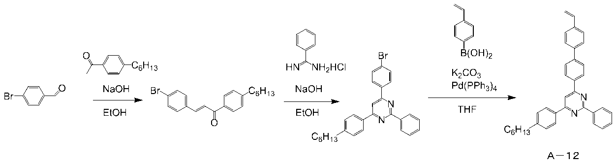
合成スキームを以下に示す。
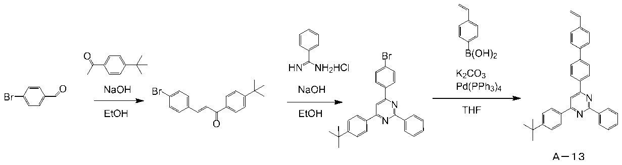
合成スキームを以下に示す。

合成スキームを以下に示す。
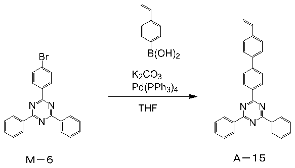
合成スキームを以下に示す。

合成スキームを以下に示す。
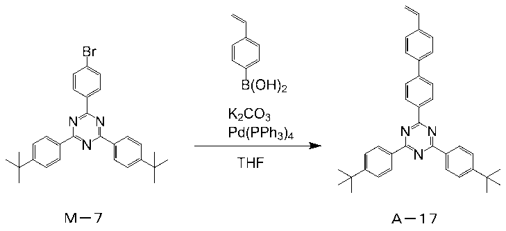
<シロキサンモノマーB-1の合成>
合成スキームを以下に示す。
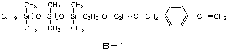
[実施例1~19]
500mgの複素環モノマーA-1~19とサイラプレーンFM-0711(JNC株式会社製)、19.7mgのパーブチルZ(日本油脂株式会社製)、2.4gのシクロヘキサノンを10mLの三口フラスコに入れ、窒素ガス封入下、110℃で30時間攪拌した。得られた反応液をメタノールに滴下し、重合体を沈殿させた後、ろ取、乾燥させることにより、本発明の重合体P-1~19を得た。

サイラプレーンFM-0711をシロキサンモノマーB-1に変更した以外は実施例1と同様にして重合体P―24~31を得た。
500mgの複素環モノマーを、250mgの複素環モノマーと250mgの第3のモノマーに変更した以外は、実施例20と同様にして重合体P-30~33を得た。
[合成例19]中間体1の合成
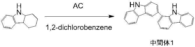

実施例1~31で得られた本発明の重合体P-1~33、並びにBYK-323(アラルキル変性ポリシロキサン,ビックケミー・ジャパン社製)を使用し、有機EL材料として発光材料を用いた電子材料組成物を製造した。
実施例1で合成した重合体P-1 0.001gを溶媒であるテトラリン9.9gに溶解させた。得られた溶液に、0.04gのトリス[2-(p-トリル)ピリジン]イリジウム(Ir(mppy)3)(Lumtec社製)と、合成例20で合成した0.26gの9,9’-(p-tert-ブチルフェニル)-1,3-ビスカルバゾールを添加し、60℃で加熱することで、電子材料組成物を製造した。
重合体P-1を実施例1~33で合成した重合体P-2~33に変更したことを除いては、実施例34と同様の方法で電子材料組成物を製造した。
重合体P-1をBYK-323に変更した以外は実施例34と同様にして、電子材料組成物を製造した。
実施例34~66および比較例で製造した電子材料組成物について以下の各種評価を行った。
有機EL素子を作製し、得らえた有機発光素子についての発光効率を評価した。
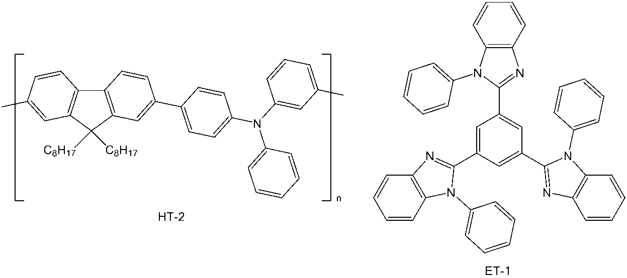
作製した有機EL素子を用いて、発光効率を評価した。
駆動安定性評価として、作製した有機EL素子を用いて、寿命を評価した。
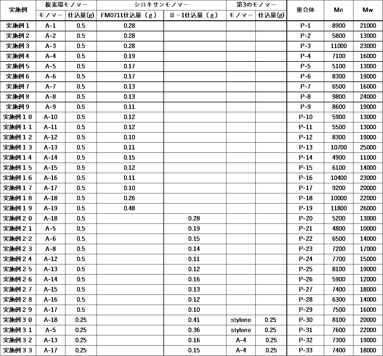
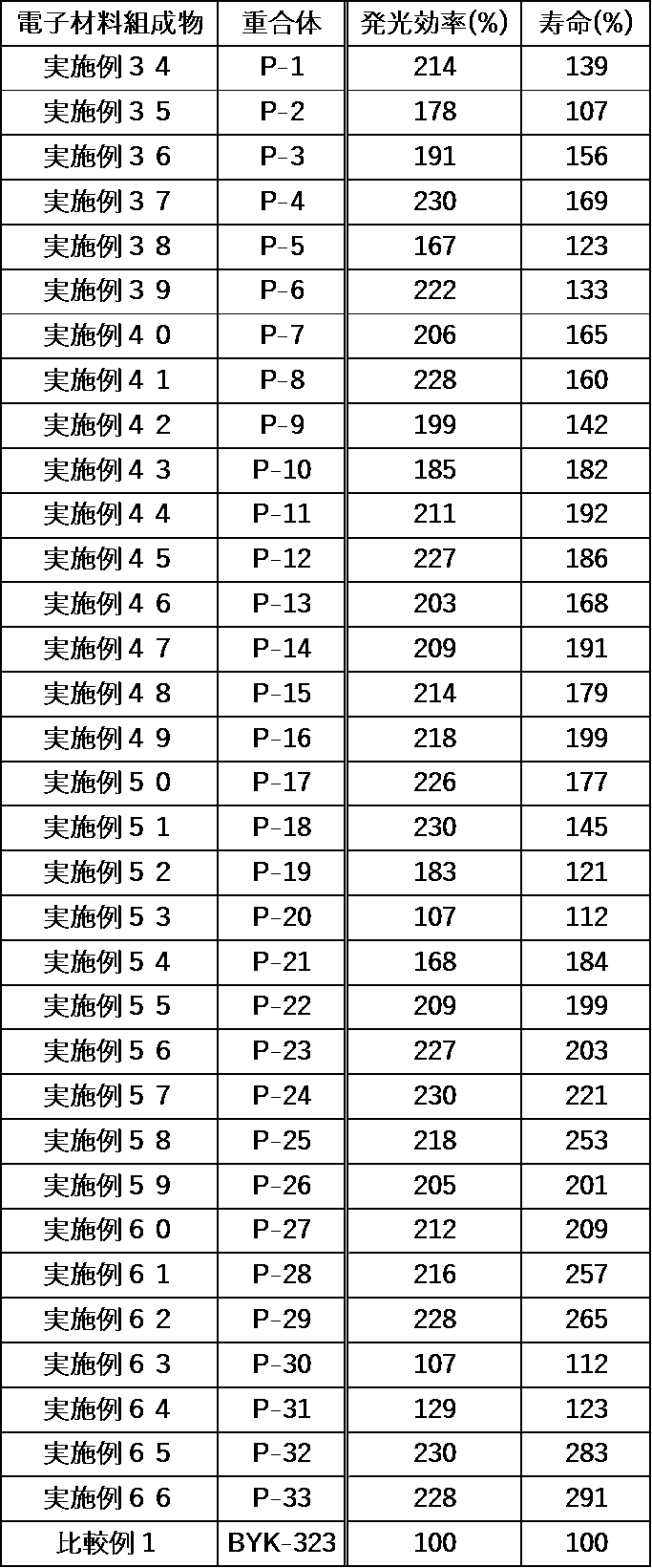
Claims (5)
- 一般式(1)で表されるモノマーと、少なくとも一般式(3)または一般式(4)で表されるモノマーを共重合してなる共重合体。

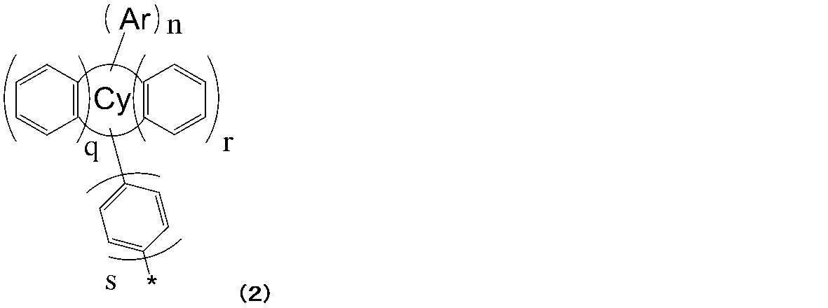
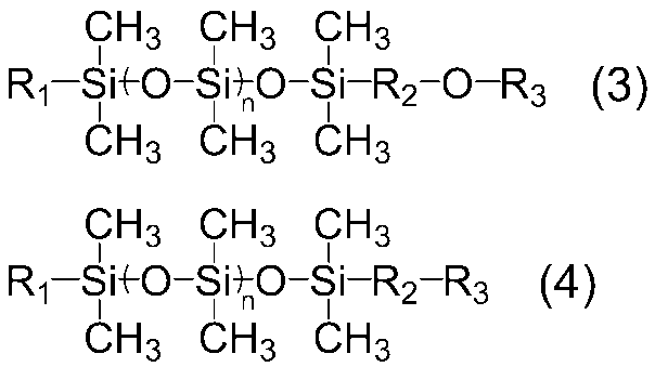
- 前記一般式(2)中、A環が下記一般式(5)~(7)から選ばれる少なくとも1つである請求項1記載の共重合体。

- 請求項1または2記載の重合体を含有することを特徴とする組成物。
- 請求項1または2記載の重合体を含有することを特徴とする電子材料組成物。
- 請求項3記載の組成物または請求項4記載の電子材料組成物を含有することを特徴とする電子素子。
Priority Applications (4)
| Application Number | Priority Date | Filing Date | Title |
|---|---|---|---|
| KR1020187012478A KR20180093881A (ko) | 2015-12-16 | 2016-08-19 | 복소환 함유 실록산 중합체, 해당 중합체를 함유하는 조성물, 전자 소자 |
| CN201680073643.6A CN108368198A (zh) | 2015-12-16 | 2016-08-19 | 含杂环的硅氧烷聚合物、含有该聚合物的组合物、电子元件 |
| US16/063,229 US20190002604A1 (en) | 2015-12-16 | 2016-08-19 | Heteroring-containing siloxane polymer, composition containing said polymer, and electronic element |
| JP2017556351A JPWO2017104173A1 (ja) | 2015-12-16 | 2016-08-19 | 複素環含有シロキサン重合体、該重合体を含有する組成物、電子素子 |
Applications Claiming Priority (2)
| Application Number | Priority Date | Filing Date | Title |
|---|---|---|---|
| JP2015-245281 | 2015-12-16 | ||
| JP2015245281 | 2015-12-16 |
Publications (1)
| Publication Number | Publication Date |
|---|---|
| WO2017104173A1 true WO2017104173A1 (ja) | 2017-06-22 |
Family
ID=59056314
Family Applications (1)
| Application Number | Title | Priority Date | Filing Date |
|---|---|---|---|
| PCT/JP2016/074229 Ceased WO2017104173A1 (ja) | 2015-12-16 | 2016-08-19 | 複素環含有シロキサン重合体、該重合体を含有する組成物、電子素子 |
Country Status (6)
| Country | Link |
|---|---|
| US (1) | US20190002604A1 (ja) |
| JP (1) | JPWO2017104173A1 (ja) |
| KR (1) | KR20180093881A (ja) |
| CN (1) | CN108368198A (ja) |
| TW (1) | TW201731884A (ja) |
| WO (1) | WO2017104173A1 (ja) |
Cited By (1)
| Publication number | Priority date | Publication date | Assignee | Title |
|---|---|---|---|---|
| JP2025032224A (ja) * | 2017-12-22 | 2025-03-11 | 株式会社半導体エネルギー研究所 | 発光素子、発光装置、電子機器、及び照明装置 |
Families Citing this family (2)
| Publication number | Priority date | Publication date | Assignee | Title |
|---|---|---|---|---|
| KR102301669B1 (ko) | 2018-08-10 | 2021-09-14 | 주식회사 엘지에너지솔루션 | 전극기재의 타발시스템 및 타발방법 |
| CN111171629A (zh) * | 2019-03-11 | 2020-05-19 | 广东聚华印刷显示技术有限公司 | 墨水及其制备方法 |
Citations (5)
| Publication number | Priority date | Publication date | Assignee | Title |
|---|---|---|---|---|
| JPH03215544A (ja) * | 1989-06-01 | 1991-09-20 | Nippon Shokubai Kagaku Kogyo Co Ltd | 耐候性塗料組成物 |
| JPH10316726A (ja) * | 1997-05-16 | 1998-12-02 | Mitsubishi Chem Corp | ベンゾフェノン基又はベンゾトリアゾール基を有するポリシロキサン系共重合体 |
| JP2001139924A (ja) * | 1999-08-30 | 2001-05-22 | Ipposha Oil Ind Co Ltd | シリコーン含有高分子紫外線吸収剤及びコーティング剤組成物 |
| WO2011013789A1 (ja) * | 2009-07-31 | 2011-02-03 | 共栄社化学株式会社 | コーティング剤用表面調整剤 |
| JP2014201735A (ja) * | 2013-04-10 | 2014-10-27 | 大日精化工業株式会社 | 高屈折率ポリマー及びその製造方法 |
Family Cites Families (4)
| Publication number | Priority date | Publication date | Assignee | Title |
|---|---|---|---|---|
| JP2014205830A (ja) | 2013-03-21 | 2014-10-30 | 国立大学法人九州大学 | 有機半導体含有層形成用レベリング剤、有機半導体含有層形成用組成物、並びに、有機デバイス及びその製造方法 |
| US20150346601A1 (en) * | 2013-04-26 | 2015-12-03 | Chi Mei Corporation | Photosensitive polysiloxane composition, protective film and element having the protective film |
| US9575423B2 (en) * | 2014-03-07 | 2017-02-21 | Kyocera Document Solutions Inc. | Electrophotographic photosensitive member |
| JP6627308B2 (ja) * | 2015-07-27 | 2020-01-08 | Jnc株式会社 | 熱硬化性組成物 |
-
2016
- 2016-08-19 JP JP2017556351A patent/JPWO2017104173A1/ja active Pending
- 2016-08-19 WO PCT/JP2016/074229 patent/WO2017104173A1/ja not_active Ceased
- 2016-08-19 US US16/063,229 patent/US20190002604A1/en not_active Abandoned
- 2016-08-19 KR KR1020187012478A patent/KR20180093881A/ko not_active Withdrawn
- 2016-08-19 CN CN201680073643.6A patent/CN108368198A/zh active Pending
- 2016-08-25 TW TW105127183A patent/TW201731884A/zh unknown
Patent Citations (5)
| Publication number | Priority date | Publication date | Assignee | Title |
|---|---|---|---|---|
| JPH03215544A (ja) * | 1989-06-01 | 1991-09-20 | Nippon Shokubai Kagaku Kogyo Co Ltd | 耐候性塗料組成物 |
| JPH10316726A (ja) * | 1997-05-16 | 1998-12-02 | Mitsubishi Chem Corp | ベンゾフェノン基又はベンゾトリアゾール基を有するポリシロキサン系共重合体 |
| JP2001139924A (ja) * | 1999-08-30 | 2001-05-22 | Ipposha Oil Ind Co Ltd | シリコーン含有高分子紫外線吸収剤及びコーティング剤組成物 |
| WO2011013789A1 (ja) * | 2009-07-31 | 2011-02-03 | 共栄社化学株式会社 | コーティング剤用表面調整剤 |
| JP2014201735A (ja) * | 2013-04-10 | 2014-10-27 | 大日精化工業株式会社 | 高屈折率ポリマー及びその製造方法 |
Cited By (1)
| Publication number | Priority date | Publication date | Assignee | Title |
|---|---|---|---|---|
| JP2025032224A (ja) * | 2017-12-22 | 2025-03-11 | 株式会社半導体エネルギー研究所 | 発光素子、発光装置、電子機器、及び照明装置 |
Also Published As
| Publication number | Publication date |
|---|---|
| CN108368198A (zh) | 2018-08-03 |
| KR20180093881A (ko) | 2018-08-22 |
| US20190002604A1 (en) | 2019-01-03 |
| JPWO2017104173A1 (ja) | 2018-05-31 |
| TW201731884A (zh) | 2017-09-16 |
Similar Documents
| Publication | Publication Date | Title |
|---|---|---|
| CN109843850B (zh) | 基于芴的化合物、使用其的有机发光器件及其制备方法 | |
| KR101999708B1 (ko) | 이온성 화합물, 이를 포함하는 코팅 조성물 및 유기 발광 소자 | |
| CN111247651B (zh) | 有机发光器件 | |
| TWI659018B (zh) | 咔唑衍生物、包含其的塗料組成物、使用其的有機發光二極體以及其製造方法 | |
| CN102781979B (zh) | 有机电致发光元件用聚合物及使用了该聚合物的有机电致发光元件 | |
| CN111247125B (zh) | 化合物、包含其的涂覆组合物和有机发光器件 | |
| KR102183737B1 (ko) | 중합체, 이를 포함하는 코팅 조성물 및 이를 이용한 유기 발광 소자 | |
| JP7427317B2 (ja) | 新規な高分子およびこれを用いた有機発光素子 | |
| KR20180092893A (ko) | 화합물, 이를 포함하는 코팅 조성물 및 이를 이용한 유기 발광 소자 | |
| KR102170399B1 (ko) | 플루오렌 유도체, 플루오렌 유도체를 포함하는 코팅 조성물 및 이를 이용하는 유기 발광 소자 | |
| JP2017119793A (ja) | 共重合体、有機エレクトロルミネッセンス素子材料、有機エレクトロルミネッセンス素子製造用組成物および有機エレクトロルミネッセンス素子 | |
| CN111247126A (zh) | 化合物、包含其的涂覆组合物和有机发光器件 | |
| CN102432844B (zh) | 树枝状聚合物和使用该树枝状聚合物的有机发光装置 | |
| JP6620015B2 (ja) | 重合体、有機エレクトロルミネッセンス素子用材料、および有機エレクトロルミネッセンス素子 | |
| JPWO2017104173A1 (ja) | 複素環含有シロキサン重合体、該重合体を含有する組成物、電子素子 | |
| US20170186950A1 (en) | Polymer, organic light-emitting device material including the same, and organic light-emitting device including the organic light-emitting device material | |
| JP2018109088A (ja) | ビニルアミノアリーレンポリマー、ならびにこれを用いた有機エレクトロルミネッセンス素子用材料および有機エレクトロルミネッセンス素子 | |
| CN113764603B (zh) | 用于有机光电器件的组合物、有机光电器件及显示器件 | |
| JP6245411B2 (ja) | シロキサンモノマーおよびその重合体、該重合体を含有する組成物、電子素子 | |
| CN120304043A (zh) | 用于有机光电装置的组成物、有机光电装置以及显示装置 | |
| KR102167242B1 (ko) | 카바졸 유도체, 이를 포함하는 코팅 조성물, 유기 발광 소자 및 이의 제조방법 | |
| KR20210010076A (ko) | 중합체, 이를 포함하는 코팅 조성물, 이를 이용한 유기 발광 소자 및 이의 제조방법 | |
| KR20210028355A (ko) | 신규한 화합물 및 이를 이용한 유기 발광 소자 | |
| JP2018104598A (ja) | 高分子化合物、ならびにこれを用いた有機エレクトロルミネッセンス素子用材料および有機エレクトロルミネッセンス素子 |
Legal Events
| Date | Code | Title | Description |
|---|---|---|---|
| 121 | Ep: the epo has been informed by wipo that ep was designated in this application |
Ref document number: 16875160 Country of ref document: EP Kind code of ref document: A1 |
|
| ENP | Entry into the national phase |
Ref document number: 2017556351 Country of ref document: JP Kind code of ref document: A |
|
| ENP | Entry into the national phase |
Ref document number: 20187012478 Country of ref document: KR Kind code of ref document: A |
|
| NENP | Non-entry into the national phase |
Ref country code: DE |
|
| 122 | Ep: pct application non-entry in european phase |
Ref document number: 16875160 Country of ref document: EP Kind code of ref document: A1 |