WO2017099145A1 - Module hyperfréquence et module haute fréquence - Google Patents
Module hyperfréquence et module haute fréquence Download PDFInfo
- Publication number
- WO2017099145A1 WO2017099145A1 PCT/JP2016/086437 JP2016086437W WO2017099145A1 WO 2017099145 A1 WO2017099145 A1 WO 2017099145A1 JP 2016086437 W JP2016086437 W JP 2016086437W WO 2017099145 A1 WO2017099145 A1 WO 2017099145A1
- Authority
- WO
- WIPO (PCT)
- Prior art keywords
- ground
- signal
- pad
- multilayer resin
- resin substrate
- Prior art date
Links
Images


Classifications
-
- H—ELECTRICITY
- H04—ELECTRIC COMMUNICATION TECHNIQUE
- H04B—TRANSMISSION
- H04B1/00—Details of transmission systems, not covered by a single one of groups H04B3/00 - H04B13/00; Details of transmission systems not characterised by the medium used for transmission
- H04B1/38—Transceivers, i.e. devices in which transmitter and receiver form a structural unit and in which at least one part is used for functions of transmitting and receiving
- H04B1/40—Circuits
-
- H—ELECTRICITY
- H01—ELECTRIC ELEMENTS
- H01L—SEMICONDUCTOR DEVICES NOT COVERED BY CLASS H10
- H01L23/00—Details of semiconductor or other solid state devices
- H01L23/552—Protection against radiation, e.g. light or electromagnetic waves
-
- H—ELECTRICITY
- H01—ELECTRIC ELEMENTS
- H01L—SEMICONDUCTOR DEVICES NOT COVERED BY CLASS H10
- H01L23/00—Details of semiconductor or other solid state devices
- H01L23/58—Structural electrical arrangements for semiconductor devices not otherwise provided for, e.g. in combination with batteries
- H01L23/64—Impedance arrangements
- H01L23/66—High-frequency adaptations
-
- H—ELECTRICITY
- H05—ELECTRIC TECHNIQUES NOT OTHERWISE PROVIDED FOR
- H05K—PRINTED CIRCUITS; CASINGS OR CONSTRUCTIONAL DETAILS OF ELECTRIC APPARATUS; MANUFACTURE OF ASSEMBLAGES OF ELECTRICAL COMPONENTS
- H05K1/00—Printed circuits
- H05K1/02—Details
- H05K1/0201—Thermal arrangements, e.g. for cooling, heating or preventing overheating
- H05K1/0203—Cooling of mounted components
- H05K1/0204—Cooling of mounted components using means for thermal conduction connection in the thickness direction of the substrate
-
- H—ELECTRICITY
- H05—ELECTRIC TECHNIQUES NOT OTHERWISE PROVIDED FOR
- H05K—PRINTED CIRCUITS; CASINGS OR CONSTRUCTIONAL DETAILS OF ELECTRIC APPARATUS; MANUFACTURE OF ASSEMBLAGES OF ELECTRICAL COMPONENTS
- H05K1/00—Printed circuits
- H05K1/02—Details
- H05K1/0213—Electrical arrangements not otherwise provided for
- H05K1/0216—Reduction of cross-talk, noise or electromagnetic interference
- H05K1/0218—Reduction of cross-talk, noise or electromagnetic interference by printed shielding conductors, ground planes or power plane
- H05K1/0219—Printed shielding conductors for shielding around or between signal conductors, e.g. coplanar or coaxial printed shielding conductors
- H05K1/0222—Printed shielding conductors for shielding around or between signal conductors, e.g. coplanar or coaxial printed shielding conductors for shielding around a single via or around a group of vias, e.g. coaxial vias or vias surrounded by a grounded via fence
-
- H—ELECTRICITY
- H05—ELECTRIC TECHNIQUES NOT OTHERWISE PROVIDED FOR
- H05K—PRINTED CIRCUITS; CASINGS OR CONSTRUCTIONAL DETAILS OF ELECTRIC APPARATUS; MANUFACTURE OF ASSEMBLAGES OF ELECTRICAL COMPONENTS
- H05K9/00—Screening of apparatus or components against electric or magnetic fields
-
- H—ELECTRICITY
- H01—ELECTRIC ELEMENTS
- H01L—SEMICONDUCTOR DEVICES NOT COVERED BY CLASS H10
- H01L2223/00—Details relating to semiconductor or other solid state devices covered by the group H01L23/00
- H01L2223/58—Structural electrical arrangements for semiconductor devices not otherwise provided for
- H01L2223/64—Impedance arrangements
- H01L2223/66—High-frequency adaptations
- H01L2223/6605—High-frequency electrical connections
- H01L2223/6611—Wire connections
-
- H—ELECTRICITY
- H01—ELECTRIC ELEMENTS
- H01L—SEMICONDUCTOR DEVICES NOT COVERED BY CLASS H10
- H01L2223/00—Details relating to semiconductor or other solid state devices covered by the group H01L23/00
- H01L2223/58—Structural electrical arrangements for semiconductor devices not otherwise provided for
- H01L2223/64—Impedance arrangements
- H01L2223/66—High-frequency adaptations
- H01L2223/6644—Packaging aspects of high-frequency amplifiers
- H01L2223/6655—Matching arrangements, e.g. arrangement of inductive and capacitive components
-
- H—ELECTRICITY
- H01—ELECTRIC ELEMENTS
- H01L—SEMICONDUCTOR DEVICES NOT COVERED BY CLASS H10
- H01L2223/00—Details relating to semiconductor or other solid state devices covered by the group H01L23/00
- H01L2223/58—Structural electrical arrangements for semiconductor devices not otherwise provided for
- H01L2223/64—Impedance arrangements
- H01L2223/66—High-frequency adaptations
- H01L2223/6661—High-frequency adaptations for passive devices
- H01L2223/6666—High-frequency adaptations for passive devices for decoupling, e.g. bypass capacitors
-
- H—ELECTRICITY
- H01—ELECTRIC ELEMENTS
- H01L—SEMICONDUCTOR DEVICES NOT COVERED BY CLASS H10
- H01L2224/00—Indexing scheme for arrangements for connecting or disconnecting semiconductor or solid-state bodies and methods related thereto as covered by H01L24/00
- H01L2224/01—Means for bonding being attached to, or being formed on, the surface to be connected, e.g. chip-to-package, die-attach, "first-level" interconnects; Manufacturing methods related thereto
- H01L2224/26—Layer connectors, e.g. plate connectors, solder or adhesive layers; Manufacturing methods related thereto
- H01L2224/31—Structure, shape, material or disposition of the layer connectors after the connecting process
- H01L2224/32—Structure, shape, material or disposition of the layer connectors after the connecting process of an individual layer connector
- H01L2224/321—Disposition
- H01L2224/32151—Disposition the layer connector connecting between a semiconductor or solid-state body and an item not being a semiconductor or solid-state body, e.g. chip-to-substrate, chip-to-passive
- H01L2224/32221—Disposition the layer connector connecting between a semiconductor or solid-state body and an item not being a semiconductor or solid-state body, e.g. chip-to-substrate, chip-to-passive the body and the item being stacked
- H01L2224/32245—Disposition the layer connector connecting between a semiconductor or solid-state body and an item not being a semiconductor or solid-state body, e.g. chip-to-substrate, chip-to-passive the body and the item being stacked the item being metallic
-
- H—ELECTRICITY
- H01—ELECTRIC ELEMENTS
- H01L—SEMICONDUCTOR DEVICES NOT COVERED BY CLASS H10
- H01L2224/00—Indexing scheme for arrangements for connecting or disconnecting semiconductor or solid-state bodies and methods related thereto as covered by H01L24/00
- H01L2224/01—Means for bonding being attached to, or being formed on, the surface to be connected, e.g. chip-to-package, die-attach, "first-level" interconnects; Manufacturing methods related thereto
- H01L2224/42—Wire connectors; Manufacturing methods related thereto
- H01L2224/47—Structure, shape, material or disposition of the wire connectors after the connecting process
- H01L2224/48—Structure, shape, material or disposition of the wire connectors after the connecting process of an individual wire connector
- H01L2224/4805—Shape
- H01L2224/4809—Loop shape
- H01L2224/48091—Arched
-
- H—ELECTRICITY
- H01—ELECTRIC ELEMENTS
- H01L—SEMICONDUCTOR DEVICES NOT COVERED BY CLASS H10
- H01L2224/00—Indexing scheme for arrangements for connecting or disconnecting semiconductor or solid-state bodies and methods related thereto as covered by H01L24/00
- H01L2224/01—Means for bonding being attached to, or being formed on, the surface to be connected, e.g. chip-to-package, die-attach, "first-level" interconnects; Manufacturing methods related thereto
- H01L2224/42—Wire connectors; Manufacturing methods related thereto
- H01L2224/47—Structure, shape, material or disposition of the wire connectors after the connecting process
- H01L2224/48—Structure, shape, material or disposition of the wire connectors after the connecting process of an individual wire connector
- H01L2224/481—Disposition
- H01L2224/48151—Connecting between a semiconductor or solid-state body and an item not being a semiconductor or solid-state body, e.g. chip-to-substrate, chip-to-passive
- H01L2224/48153—Connecting between a semiconductor or solid-state body and an item not being a semiconductor or solid-state body, e.g. chip-to-substrate, chip-to-passive the body and the item being arranged next to each other, e.g. on a common substrate
- H01L2224/48155—Connecting between a semiconductor or solid-state body and an item not being a semiconductor or solid-state body, e.g. chip-to-substrate, chip-to-passive the body and the item being arranged next to each other, e.g. on a common substrate the item being non-metallic, e.g. insulating substrate with or without metallisation
-
- H—ELECTRICITY
- H01—ELECTRIC ELEMENTS
- H01L—SEMICONDUCTOR DEVICES NOT COVERED BY CLASS H10
- H01L2224/00—Indexing scheme for arrangements for connecting or disconnecting semiconductor or solid-state bodies and methods related thereto as covered by H01L24/00
- H01L2224/73—Means for bonding being of different types provided for in two or more of groups H01L2224/10, H01L2224/18, H01L2224/26, H01L2224/34, H01L2224/42, H01L2224/50, H01L2224/63, H01L2224/71
- H01L2224/732—Location after the connecting process
- H01L2224/73251—Location after the connecting process on different surfaces
- H01L2224/73265—Layer and wire connectors
-
- H—ELECTRICITY
- H01—ELECTRIC ELEMENTS
- H01L—SEMICONDUCTOR DEVICES NOT COVERED BY CLASS H10
- H01L2924/00—Indexing scheme for arrangements or methods for connecting or disconnecting semiconductor or solid-state bodies as covered by H01L24/00
- H01L2924/10—Details of semiconductor or other solid state devices to be connected
- H01L2924/11—Device type
- H01L2924/14—Integrated circuits
- H01L2924/141—Analog devices
- H01L2924/142—HF devices
- H01L2924/1421—RF devices
- H01L2924/14215—Low-noise amplifier [LNA]
-
- H—ELECTRICITY
- H01—ELECTRIC ELEMENTS
- H01L—SEMICONDUCTOR DEVICES NOT COVERED BY CLASS H10
- H01L2924/00—Indexing scheme for arrangements or methods for connecting or disconnecting semiconductor or solid-state bodies as covered by H01L24/00
- H01L2924/15—Details of package parts other than the semiconductor or other solid state devices to be connected
- H01L2924/151—Die mounting substrate
- H01L2924/1517—Multilayer substrate
- H01L2924/15192—Resurf arrangement of the internal vias
-
- H—ELECTRICITY
- H01—ELECTRIC ELEMENTS
- H01L—SEMICONDUCTOR DEVICES NOT COVERED BY CLASS H10
- H01L2924/00—Indexing scheme for arrangements or methods for connecting or disconnecting semiconductor or solid-state bodies as covered by H01L24/00
- H01L2924/15—Details of package parts other than the semiconductor or other solid state devices to be connected
- H01L2924/151—Die mounting substrate
- H01L2924/153—Connection portion
- H01L2924/1531—Connection portion the connection portion being formed only on the surface of the substrate opposite to the die mounting surface
- H01L2924/15311—Connection portion the connection portion being formed only on the surface of the substrate opposite to the die mounting surface being a ball array, e.g. BGA
-
- H—ELECTRICITY
- H01—ELECTRIC ELEMENTS
- H01L—SEMICONDUCTOR DEVICES NOT COVERED BY CLASS H10
- H01L2924/00—Indexing scheme for arrangements or methods for connecting or disconnecting semiconductor or solid-state bodies as covered by H01L24/00
- H01L2924/15—Details of package parts other than the semiconductor or other solid state devices to be connected
- H01L2924/151—Die mounting substrate
- H01L2924/153—Connection portion
- H01L2924/1531—Connection portion the connection portion being formed only on the surface of the substrate opposite to the die mounting surface
- H01L2924/15313—Connection portion the connection portion being formed only on the surface of the substrate opposite to the die mounting surface being a land array, e.g. LGA
-
- H—ELECTRICITY
- H01—ELECTRIC ELEMENTS
- H01L—SEMICONDUCTOR DEVICES NOT COVERED BY CLASS H10
- H01L2924/00—Indexing scheme for arrangements or methods for connecting or disconnecting semiconductor or solid-state bodies as covered by H01L24/00
- H01L2924/15—Details of package parts other than the semiconductor or other solid state devices to be connected
- H01L2924/161—Cap
- H01L2924/162—Disposition
- H01L2924/16251—Connecting to an item not being a semiconductor or solid-state body, e.g. cap-to-substrate
-
- H—ELECTRICITY
- H01—ELECTRIC ELEMENTS
- H01L—SEMICONDUCTOR DEVICES NOT COVERED BY CLASS H10
- H01L2924/00—Indexing scheme for arrangements or methods for connecting or disconnecting semiconductor or solid-state bodies as covered by H01L24/00
- H01L2924/19—Details of hybrid assemblies other than the semiconductor or other solid state devices to be connected
- H01L2924/1901—Structure
- H01L2924/1904—Component type
- H01L2924/19041—Component type being a capacitor
-
- H—ELECTRICITY
- H01—ELECTRIC ELEMENTS
- H01L—SEMICONDUCTOR DEVICES NOT COVERED BY CLASS H10
- H01L2924/00—Indexing scheme for arrangements or methods for connecting or disconnecting semiconductor or solid-state bodies as covered by H01L24/00
- H01L2924/19—Details of hybrid assemblies other than the semiconductor or other solid state devices to be connected
- H01L2924/191—Disposition
- H01L2924/19101—Disposition of discrete passive components
- H01L2924/19105—Disposition of discrete passive components in a side-by-side arrangement on a common die mounting substrate
-
- H—ELECTRICITY
- H01—ELECTRIC ELEMENTS
- H01L—SEMICONDUCTOR DEVICES NOT COVERED BY CLASS H10
- H01L2924/00—Indexing scheme for arrangements or methods for connecting or disconnecting semiconductor or solid-state bodies as covered by H01L24/00
- H01L2924/19—Details of hybrid assemblies other than the semiconductor or other solid state devices to be connected
- H01L2924/191—Disposition
- H01L2924/19101—Disposition of discrete passive components
- H01L2924/19107—Disposition of discrete passive components off-chip wires
-
- H—ELECTRICITY
- H01—ELECTRIC ELEMENTS
- H01L—SEMICONDUCTOR DEVICES NOT COVERED BY CLASS H10
- H01L2924/00—Indexing scheme for arrangements or methods for connecting or disconnecting semiconductor or solid-state bodies as covered by H01L24/00
- H01L2924/30—Technical effects
- H01L2924/301—Electrical effects
- H01L2924/3011—Impedance
- H01L2924/30111—Impedance matching
-
- H—ELECTRICITY
- H01—ELECTRIC ELEMENTS
- H01L—SEMICONDUCTOR DEVICES NOT COVERED BY CLASS H10
- H01L2924/00—Indexing scheme for arrangements or methods for connecting or disconnecting semiconductor or solid-state bodies as covered by H01L24/00
- H01L2924/30—Technical effects
- H01L2924/301—Electrical effects
- H01L2924/3025—Electromagnetic shielding
-
- H—ELECTRICITY
- H05—ELECTRIC TECHNIQUES NOT OTHERWISE PROVIDED FOR
- H05K—PRINTED CIRCUITS; CASINGS OR CONSTRUCTIONAL DETAILS OF ELECTRIC APPARATUS; MANUFACTURE OF ASSEMBLAGES OF ELECTRICAL COMPONENTS
- H05K1/00—Printed circuits
- H05K1/02—Details
- H05K1/14—Structural association of two or more printed circuits
- H05K1/144—Stacked arrangements of planar printed circuit boards
-
- H—ELECTRICITY
- H05—ELECTRIC TECHNIQUES NOT OTHERWISE PROVIDED FOR
- H05K—PRINTED CIRCUITS; CASINGS OR CONSTRUCTIONAL DETAILS OF ELECTRIC APPARATUS; MANUFACTURE OF ASSEMBLAGES OF ELECTRICAL COMPONENTS
- H05K2201/00—Indexing scheme relating to printed circuits covered by H05K1/00
- H05K2201/03—Conductive materials
- H05K2201/0302—Properties and characteristics in general
- H05K2201/0311—Metallic part with specific elastic properties, e.g. bent piece of metal as electrical contact
-
- H—ELECTRICITY
- H05—ELECTRIC TECHNIQUES NOT OTHERWISE PROVIDED FOR
- H05K—PRINTED CIRCUITS; CASINGS OR CONSTRUCTIONAL DETAILS OF ELECTRIC APPARATUS; MANUFACTURE OF ASSEMBLAGES OF ELECTRICAL COMPONENTS
- H05K2201/00—Indexing scheme relating to printed circuits covered by H05K1/00
- H05K2201/10—Details of components or other objects attached to or integrated in a printed circuit board
- H05K2201/10227—Other objects, e.g. metallic pieces
- H05K2201/10371—Shields or metal cases
-
- H—ELECTRICITY
- H05—ELECTRIC TECHNIQUES NOT OTHERWISE PROVIDED FOR
- H05K—PRINTED CIRCUITS; CASINGS OR CONSTRUCTIONAL DETAILS OF ELECTRIC APPARATUS; MANUFACTURE OF ASSEMBLAGES OF ELECTRICAL COMPONENTS
- H05K2201/00—Indexing scheme relating to printed circuits covered by H05K1/00
- H05K2201/10—Details of components or other objects attached to or integrated in a printed circuit board
- H05K2201/10227—Other objects, e.g. metallic pieces
- H05K2201/10416—Metallic blocks or heatsinks completely inserted in a PCB
-
- H—ELECTRICITY
- H05—ELECTRIC TECHNIQUES NOT OTHERWISE PROVIDED FOR
- H05K—PRINTED CIRCUITS; CASINGS OR CONSTRUCTIONAL DETAILS OF ELECTRIC APPARATUS; MANUFACTURE OF ASSEMBLAGES OF ELECTRICAL COMPONENTS
- H05K3/00—Apparatus or processes for manufacturing printed circuits
- H05K3/0058—Laminating printed circuit boards onto other substrates, e.g. metallic substrates
- H05K3/0061—Laminating printed circuit boards onto other substrates, e.g. metallic substrates onto a metallic substrate, e.g. a heat sink
-
- H—ELECTRICITY
- H05—ELECTRIC TECHNIQUES NOT OTHERWISE PROVIDED FOR
- H05K—PRINTED CIRCUITS; CASINGS OR CONSTRUCTIONAL DETAILS OF ELECTRIC APPARATUS; MANUFACTURE OF ASSEMBLAGES OF ELECTRICAL COMPONENTS
- H05K3/00—Apparatus or processes for manufacturing printed circuits
- H05K3/36—Assembling printed circuits with other printed circuits
- H05K3/368—Assembling printed circuits with other printed circuits parallel to each other
Definitions
- the present invention relates to a microwave module and a high frequency module.
- a substrate made of resin or ceramic on which a part of RF devices is mounted, HPA A high heat generation RF device such as (High Power Amplifier) and an RF connector are fixed to a metal chassis with screws or a bonding agent. Then, the substrate and the high heat generation RF device are bonded and connected by a gold ribbon or a gold wire.
- RF Radio Frequency
- the electromagnetic waves are emitted from the RF devices and signal lines exposed to space, particularly from the connection point of the gold ribbon or the gold wire connecting the RF devices and the substrate, the spatial isolation is degraded by the radiation and coupling of the electromagnetic waves. It is necessary to suppress the characteristic failure and the unstable operation caused.
- the metal cover which took the space isolation improvement measures such as an electromagnetic shielding which divides a space, or an electromagnetic wave absorber, is arrange
- Patent Document 1 a metal cover surrounding a plurality of RF devices is required, and in order to suppress coupling and resonance due to electromagnetic waves generated inside the metal cover, an electromagnetic shield or Measures such as installation of a radio wave absorber are required. Therefore, in the above-mentioned prior art, there was a problem that cost increased.
- This invention is made in view of the above, Comprising: It aims at obtaining the microwave module and high frequency module which can suppress the raise of cost.
- the microwave module according to the present invention is implemented by a plurality of first microwave devices having a microwave circuit and an electromagnetic shield wall covering at least the microwave circuit.
- a multilayer resin substrate having a second surface ground connected to the pad and a heat dissipation body
- FIG. 2 A view of the device substrate shown in FIG. 3 as viewed from the fourth end face side
- FIG. 9 is a perspective view of the contact terminal shown in FIG. A view from the fifth end face side of the distribution circuit board shown in FIG. 9 XIII-XIII arrow sectional drawing of the microwave module concerning Embodiment 1 Sectional drawing which shows the connection state of the microwave module and antenna which concern on Embodiment 2.
- Partial cross-sectional view of the microwave module according to the first and second embodiments The figure for demonstrating the effect by the contact terminal provided in the microwave module concerning Embodiment 2.
- a partial enlarged view of the microwave module shown in FIG. The figure which shows the modification of the multilayer resin substrate shown in FIG.
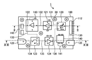
- FIG. 1 is a front view of the microwave module according to the first embodiment.
- FIG. 2 is a cross-sectional view taken along the line II-II of the microwave module shown in FIG.
- FIG. 3 is a detailed view of the RF device shown in FIG.
- FIG. 4 is a view of the device substrate shown in FIG. 2 as viewed from the fourth end face side.
- FIG. 5 is a view of the multilayer resin substrate shown in FIG. 1 as viewed from the first end face side.
- FIG. 6 is a view showing an inner layer portion of the multilayer resin substrate shown in FIG. 7 is a cross-sectional view of the device substrate shown in FIG. 3 and the multilayer resin substrate shown in FIGS.
- FIG. 8 is a cross-sectional view of a surface including the surface ground on the first end face side, the inner surface surface ground, and two ground through holes in the multilayer resin substrate shown in FIG. 7.
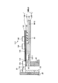
- the microwave module 1 is composed of a multilayer resin substrate 100 having a first end face 101 and a second end face 102 opposite to the first end face 101 as shown in FIG.
- the microwave module 1 is mechanically and thermally connected to the cooling plate 300 disposed on the second end surface 102 side of the multilayer resin substrate 100.
- the multilayer resin substrate 100 of the microwave module 1 is fixed to the cooling plate 300 by a fixing screw 30 as shown in FIG.
- the one or more microwave modules 1 are fixed to the cooling plate 300 to constitute the microwave module 500 together with the cooling plate 300 as shown in FIG.
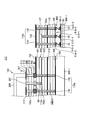
- a plurality of first microwave devices RF devices 120, 121, 122, 123, 124 and a plurality of bypass capacitors are provided on the first end face 101 side of the multilayer resin substrate 100.
- a plurality of first microwave devices RF devices 120, 121, 122, 123, 124 and a plurality of bypass capacitors are provided on the first end face 101 side of the multilayer resin substrate 100.
- 141, 142 and 143 are provided on the first end face 101 side of the multilayer resin substrate 100.
- a feeding circuit side coaxial RF connector 125 an antenna side coaxial RF connector 126, a control IC (Integrated Circuit) 140, and a power control connector 112 are provided. There is.
- the RF device 120 is a phase shifter and a switch.
- the RF device 121 is a driver amplifier
- the RF device 122 is an HPA
- the RF device 123 is a circulator or a high power switch
- the RF device 124 is a low noise amplifier.
- the multilayer resin substrate 100 As shown in FIGS. 1 and 2, inside the multilayer resin substrate 100, a plurality of RF transmission lines 130 to 136 and a heat radiation embedded member 175 which is a first heat radiation body are provided inside the multilayer resin substrate 100. Specifically, the multilayer resin substrate 100 has the heat radiation embedded member 175 connected to the internal circuit 220 in a region formed by projecting the internal circuit 220 which is the microwave circuit shown in FIG. 3 toward the multilayer resin substrate 100. Have.
- the feeding circuit side coaxial RF connector 125 and the RF device 120 are connected by the RF transmission line 130.
- the RF device 120 and the RF device 121 are connected by an RF transmission line 131.
- the RF device 121 and the RF device 122 are connected by an RF transmission line 132 which is an inner layer signal line.
- the RF device 122 and the RF device 123 are connected by an RF transmission line 133 which is an inner layer signal line.
- the RF device 123 and the antenna-side coaxial RF connector 126 are connected by an RF transmission line 134.
- the RF device 123 and the RF device 124 are connected by an RF transmission line 135.
- the RF device 124 and the RF device 120 are connected by an RF transmission line 136.
- the feed circuit side coaxial RF connector 125 and the antenna side coaxial RF connector 126 are covered with the outer conductor, respectively, and the RF devices 120, 121, 122, 123 and 124 are provided with ground through holes, metal cover or metal plating on the device outer peripheral surface. Covered with a dielectric that has
- one end of the heat radiation embedding member 175 is connected to the RF device 122.
- the other end of the heat radiation embedding member 175 is connected to the cooling plate 300.
- the heat radiation embedding member 175 is a heat radiating body for effectively transferring the heat generated by the RF device 122 to the cooling plate 300, and is formed of a metal such as copper, aluminum, or a copper alloy.
- the shape of the heat radiation embedding member 175 is a cylinder or a square pole.
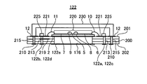
- FIG. 1 An exemplary configuration of the RF device 122 is shown in FIG.
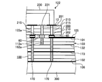
- the RF device 122 has a device substrate 200 having a third end face 201 and a fourth end face 202 opposite to the third end face 201.
- the RF device 122 includes the metal plate 2 provided on the third end face 201, the internal circuit 220 which is a microwave circuit provided on the metal plate 2, and the third end face 201 surrounding the internal circuit 220. It has a signal line 221 provided on top and a ground pattern 12.
- the RF device 122 also has a bypass capacitor 225 that suppresses RF superimposed waves, and a metal cover 230 which is an electromagnetic shield wall.
- the metal plate 2 is a plate for thermal expansion coefficient matching formed of an alloy or the like of copper and molybdenum.
- the metal plate 2 is attached on the third end face 201 by bonding or soldering.
- the internal circuit 220 includes a transistor chip 5 disposed on the top surface of the metal plate 2, an input matching circuit 6, and an output matching circuit 7.
- the transistor chip 5 is disposed between the input matching circuit 6 and the output matching circuit 7.
- the transistor chip 5, the input matching circuit 6 and the output matching circuit 7 are mounted on the surface of the metal plate 2 by bonding or soldering.
- the transistor chip 5 and the input matching circuit 6 are connected by a bonding wire 8.
- the transistor chip 5 and the output matching circuit 7 are connected by a bonding wire 9.
- the input matching circuit 6 and the signal line 221 are connected by the bonding wire 10.
- the output matching circuit 7 and the signal line 221 are connected by the bonding wire 11.
- Types of the signal line 221 include an input RF line, a gate bias supply line, an output RF line, and a drain bias supply line.
- the gate bias supply line is a line for supplying a gate bias to the internal circuit 220.
- the drain bias supply line is a line that supplies the internal circuit 220 with a drain bias.
- the ground pattern 12 is provided outside the signal line 221 on the third end face 201 of the device substrate 200. That is, the ground pattern 12 is provided on the third end face 201 of the device substrate 200 so as to surround the internal circuit 220, the signal line 221 and the bypass capacitor 225.
- the metal cover 230 is provided on the third end face 201 side of the device substrate 200 so as to cover the internal circuit 220, the signal line 221, and the bypass capacitor 225.
- the metal cover 230 is also connected to the ground pattern 12 by adhesion or soldering.
- the material used for the metal cover 230 is iron, stainless steel, aluminum, copper, brass or the like. It may be a metal-plated dielectric.
- the device substrate 200 internally includes a plurality of signal through holes 213 connected to the signal line 221, a plurality of ground through holes 215, and a heat radiation embedded member 176.
- the heat radiation embedded member 176 which is a second heat radiating body is provided at the central portion of the device substrate 200 below the internal circuit 220.
- One end face of the heat radiation embedding member 176 is connected to the metal plate 2.
- the other end face of the heat radiation embedding member 176 is connected to a ground pad 122 e which is a termination terminal of the heat radiation embedding member 176.
- the heat radiation embedding member 176 is a heat radiating body for effectively transferring the heat generated by the RF device 122 to the cooling plate 300.
- the heat radiation embedded member 176 is formed of a metal such as copper, aluminum or copper alloy.
- the shape of the heat radiation embedding member 176 is a cylinder or a square pole.
- the plurality of signal through holes 213 are provided inside the device substrate 200 so as to surround the metal plate 2 and the internal circuit 220.
- the plurality of ground through holes 215 are provided outside the position where the plurality of signal through holes 213 are provided.
- the plurality of ground through holes 215 are provided inside the device substrate 200 so as to surround the plurality of signal through holes 213.
- the plurality of ground through holes 215 are connected to the ground pattern 12.
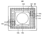
- the device substrate 200 has an input RF signal terminal 122a, an output RF signal terminal 122b, a gate control terminal 122c, and a terminal for exchanging signals with the multilayer resin substrate 100 at the fourth end face 202. It has a drain power supply terminal 122d.
- the device substrate 200 has a plurality of ground terminals 210 and ground pads 122 e at the fourth end face 202.
- the input RF signal terminal 122a is connected to the signal through hole 213 for the input RF line shown in FIG.
- the output RF signal terminal 122b is connected to the signal through hole 213 for the output RF line shown in FIG.
- the gate control terminal 122c is connected to the signal through hole 213 for the gate bias supply line shown in FIG.
- the drain power supply terminal 122 d is connected to the signal through hole 213 for the drain bias supply line shown in FIG. 3.
- the input RF signal terminal 122 a, the output RF signal terminal 122 b, the gate control terminal 122 c, and the drain power supply terminal 122 d are connected to the signal line 221 via the signal through holes 213 respectively.
- the plurality of ground terminals 210 are respectively connected to the plurality of ground through holes 215.
- a pseudo-coaxial is formed by surrounding the input RF signal terminal 122a with eight ground terminals 210 adjacent to the input RF signal terminal 122a.
- a pseudo-coaxial is formed by surrounding the output RF signal terminal 122b with eight ground terminals 210 adjacent to the output RF signal terminal 122b.
- the plurality of ground terminals 210 are connected to the ground pattern 12 via the ground through holes 215, respectively. That is, each of the plurality of ground terminals 210 is connected to the metal cover 230.
- a bypass capacitor 225 for suppressing an RF superimposed wave and an RF signal suppression filter 219 shown in FIG. 3 are disposed on the gate control terminal 122c and the drain power supply terminal 122d in accordance with the superimposed wave.
- the input RF signal terminal 122a, the output RF signal terminal 122b, the gate control terminal 122c, and the drain power supply terminal 122d are surrounded by the metal cover 230, the plurality of ground through holes 215, and the plurality of ground terminals 210. Is located in
- the internal circuit 220, the signal line 221, and the bypass capacitor 225 are electromagnetically shielded by mounting on the multilayer resin substrate 100 described later, and the electromagnetic wave generated by the RF device 122 is radiated to the outside of the RF device 122. Can be suppressed.
- the RF devices 121, 123 and 124 shown in FIG. 1 are electromagnetically shielded by being covered with a metal cover or a metal-plated dielectric as in the case of the RF device 122 having the electromagnetic shielding shown in FIG. It is assumed that the electromagnetic shielding wall which has the above configuration is provided.
- the multilayer resin substrate 100 has lands 112a, lands 112b, lands 112c, and lands 112d at its first end face 101. As shown in FIG.
- the multilayer resin substrate 100 also has lands 113a, lands 113b, lands 113c, lands 116a, lands 117a, and lands 118a on the first end face 101 thereof.
- the multilayer resin substrate 100 also has a surface ground 105 which is a first surface ground in the region other than the lands described above at the first end face 101.
- the land 112a is connected to the input RF signal terminal 122a.
- Land 112b is connected to output RF signal terminal 122b.
- the land 112c is connected to the gate control terminal 122c.
- the land 112 d is connected to the drain power supply terminal 122 d.
- the lands 113a, 113b and 113c are connected to signal terminals (not shown) provided in the RF device 123 shown in FIG.
- the land 116a is connected to a signal terminal (not shown) provided on the antenna-side coaxial RF connector 126 shown in FIG.
- the land 117a is connected to one signal terminal of the bypass capacitor 143 shown in FIG.
- the land 118a is connected to one signal terminal of the bypass capacitor 142 shown in FIG.
- FIG. 5 shows only the region on the side of the antenna not shown in the multilayer resin substrate 100, the same configuration is also applied to other regions.
- the multilayer resin substrate 100 has an RF signal suppression filter 157, an RF transmission line 132, an RF transmission line 133, a signal through hole 162a, and a first signal through in an inner layer portion 103 thereof. It has a signal through hole 162b which is a hole, a signal through hole 162c, and a signal through hole 162d.
- the multilayer resin substrate 100 also has, in the inner layer portion 103, a through hole 167a, a through hole 168a, a plurality of ground through holes 170, a gate control signal line 152c, and a drain power supply line 152d.
- an inner layer surface ground 173 is provided in the inner layer portion 103 of the multilayer resin substrate 100.
- a surface ground 106 which is a second surface ground is provided.
- the heat radiation embedded member 175 is provided on the multilayer resin substrate 100 so as to be surrounded by the four signal through holes 162 a, 162 b, 162 c and 162 d and further surrounded by a plurality of ground through holes 170.
- the signal through holes 162a are connected to the lands 112a shown in FIG. 5 and to the RF transmission line 132 shown in FIG.
- the signal through holes 162b are connected to the lands 112b shown in FIG. 5 and to the RF transmission line 133 shown in FIG.
- the signal through holes 162c are connected to the lands 112c shown in FIG. 5 and to the gate control signal line 152c shown in FIG.
- the signal through holes 162 d are connected to the lands 112 d shown in FIG. 5 and to the drain power supply line 152 d shown in FIG.
- Through holes 167a are connected to lands 117a shown in FIG.
- Through holes 168a are connected to lands 118a shown in FIG. 5 and to drain power supply line 152d.
- Each of the plurality of ground through holes 170 is connected to the surface ground 105 and the surface ground 106 shown in FIG.
- the input RF signal terminal 122a of the RF device 122 shown in FIG. 4 is connected to the RF transmission line 132 via the land 112a shown in FIG. 5 and the signal through hole 162a shown in FIG.
- the output RF signal terminal 122b of the RF device 122 shown in FIG. 4 is connected to the RF transmission line 133 shown in FIG. 6 via the land 112b shown in FIG. 5 and the signal through hole 162b shown in FIG.
- the gate control terminal 122c of the RF device 122 shown in FIG. 4 is connected to the gate control signal line 152c shown in FIG. 6 via the land 112c shown in FIG. 5 and the signal through hole 162c shown in FIG.
- the drain power supply terminal 122d of the RF device 122 shown in FIG. 4 is connected to the drain power supply line 152d shown in FIG. 6 via the land 112d shown in FIG. 5 and the signal through hole 162d shown in FIG.
- the RF signal superimposed on the gate control terminal 122 c and the drain power supply terminal 122 d shown in FIG. 4 is attenuated by the bypass capacitor 225 disposed inside the RF device 122 and a filter circuit (not shown), and the multilayer resin substrate 100 is formed.
- the leakage of the RF signal to the gate control signal line 152c and the drain power supply line 152d is suppressed.
- an RF signal suppression filter 157 for a gate control signal line is further provided in the multilayer resin substrate 100 according to the amount of attenuation inside the RF device 122, and the RF signal superimposed on the gate control signal line 152c is It is suppressed.
- the bypass capacitor 143 connected through the through hole 167a is a capacitor for suppressing the low frequency oscillation of the RF device 122, and the bypass capacitor 142 connected through the through hole 168a similarly suppresses the low frequency oscillation and charges. It is a capacitor attached for the purpose of supply.
- the RF transmission line 132 in the multilayer resin substrate 100 is surrounded by the ground of the same potential.
- the signal through holes 213 and the ground through holes 215 in the device substrate 200 constitute pseudo coaxial lines in the device substrate 200.
- the signal through holes 162 a and the ground through holes 170 in the multilayer resin substrate 100 constitute pseudo coaxial lines in the multilayer resin substrate 100.
- the signal through hole 213 of the RF device 122 is connected to the RF transmission line 132 via the input RF signal terminal 122a, the solder layer 60, the land 112a, and the signal through hole 162a.
- the ground through hole 215 of the RF device 122 is connected to the surface ground 106 via the ground terminal 210, the solder layer 60, the surface ground 105, and the ground through hole 170.
- the RF transmission line 132 inside the multilayer resin substrate 100 is surrounded by the surface ground 105, the inner layer surface ground 173, and two ground through holes 170.
- the cooling plate 300, the surface ground 105, the surface ground 106, the inner surface ground 173, the ground through hole 170, the ground through hole 215, and the metal cover 230 form an electrical ground of the same potential, that is, a pseudo electric wall.
- the signal output from the RF device 122 is transmitted to an RF device configured in the same manner as the RF device 122 without being radiated to the outside since it is entirely surrounded by the same ground.
- microwave module 1 The operation of the microwave module 1 and the microwave module 500 will be described below.
- the drain power in the RF device 122 is supplied from the power control connector 112 to the RF device 122 via the control IC 140 and the bypass capacitors 141, 142 and 143.
- a device control signal including a gate control signal in the RF device 122 is transmitted from the power control connector 112 to the RF device 122 via the control IC 140 to operate the RF device 122 in a required state.
- the transmission seed signal is input to the feeding circuit side coaxial RF connector 125 and transmitted from the feeding circuit side coaxial RF connector 125 to the RF device 120 via the RF transmission line 130.
- the transmission seed signal transmitted to the RF device 120 is transmitted in order of the RF device 121, the RF device 122, the RF device 123, and the antenna-side coaxial RF connector 126.
- the transmission seed signal is amplified and phase-controlled in the process, and radiated to space via an antenna (not shown).
- a signal wave received by an antenna is input to the antenna-side coaxial RF connector 126 as a received signal, and transmitted from the antenna-side coaxial RF connector 126 to the RF device 123 via the RF transmission line 134.
- the received signal transmitted to the RF device 123 is transmitted in the order of the RF device 124, the RF device 120, and the feeding circuit side coaxial RF connector 125, and is signal-combined by a distribution circuit (not shown).
- the heat generated by the RF device 122 is transmitted to the cooling plate 300 via the heat radiation embedded member 176, the ground pad 122e, and the heat radiation embedded member 175. This effectively cools the RF device 122.
- the RF devices 120, 121, 123, 124 other than the RF device 122 are each effectively cooled by the heat radiation embedded member or through hole according to the amount of heat generation.
- the plurality of RF devices, the signal line, and the RF transmission line are stored in the pseudo electric wall. Therefore, electromagnetic waves generated inside the plurality of RF devices can be suppressed from being radiated to the outside of the respective RF devices.
- the conventional module requires a module cover of metal such as metal that collectively encloses a plurality of RF devices, and furthermore, installation of an electromagnetic shield or a radio wave absorber to ensure space isolation between the RF device terminals. And the cost has risen.
- the microwave module 1 according to the first embodiment does not need such a module cover, and further, there is no need to install an electromagnetic shield or a radio wave absorber inside such a module cover. Therefore, cost reduction, miniaturization, and weight reduction are possible.
- the microwave module 1 of the first embodiment It is configured to be surface mounted on top. Therefore, cost reduction, size reduction, and weight reduction are possible.
- the microwave module 1 since a plurality of RF devices are surface mounted on the multilayer resin substrate 100, a chassis individually prepared as a module unit structure is not necessary, and the direct cooling plate 300 is provided.
- the multilayer resin substrate 100 can be fixed. Therefore, cost reduction, size reduction, and weight reduction are possible.
- the heat radiation embedded member 176 is provided in a high heat generation RF device such as HPA, and the heat radiation embedded member 175 is provided in the multilayer resin substrate 100.
- HPA high heat generation RF device
- the heat radiation embedded member 175 is provided in the multilayer resin substrate 100.
- microwave module 500 of the first embodiment it is possible to avoid an increase in mass accompanying the installation of the conventional chassis, module cover, and resonance suppression component.
- FIG. 9 is a cross-sectional view of the microwave module according to the second embodiment.
- FIG. 10 is a view seen from the second end face side of the multilayer resin substrate shown in FIG.
- FIG. 11 is a perspective view of the contact terminal shown in FIG.
- FIG. 12 is a view seen from the fifth end face side of the distribution circuit board shown in FIG.
- the microwave module 1-1 according to the second embodiment mainly differs from the microwave module 1 according to the first embodiment in the following points.
- a multilayer resin substrate 100-1 corresponding to the multilayer resin substrate 100 is used.
- An RF device 123-1 corresponding to the RF device 123 which is a non-shielded microwave device which is not electromagnetically shielded and which will be described later, is used.
- the RF device 123-1 is provided on the second end face 102 of the multilayer resin substrate 100-1.
- a plurality of lands 183 for the RF device 123-1 are provided on the second end face 102 of the multilayer resin substrate 100-1 so as to surround the RF device 123-1.
- a power control connector pad 52A and a power control connector terminal 52B are provided instead of the power control connector 112. However, the power control connector 112 may be provided.
- the RF connector pad 51A and the power control connector pad 52A are provided on the second end face 102 of the multilayer resin substrate 100-1 at positions facing the contact terminals 55 described later.
- the microwave module 500-1 of the second embodiment mainly differs from the microwave module 500 of the first embodiment in the following points.
- the microwave module 500-1 is composed of one or more microwave modules 1-1 and a cooling plate 300-1 corresponding to the cooling plate 300.
- a cavity 15 for storing the RF device 123-1 and the land 183 is formed.
- the cooling plate 300-1 is provided with a distribution circuit board 50 which is a circuit board for supplying power, control signals, and RF signals to the devices on the multilayer resin substrate 100-1.
- a contact terminal 55 mounted on the surface of the distribution circuit board 50 and having a spring property is provided.
- the distribution circuit board 50 shown in FIG. 9 has a fifth end face 50-1 and a sixth end face 50-2 opposite to the fifth end face 50-1.
- the RF device 120 and the RF device 121 are connected by an RF transmission line 131 which is an inner layer signal line, and the RF device 121 and the RF device 122 are connected by an RF transmission line 132 which is an inner layer signal line.
- 55 are connected by an RF transmission line 136 which is an inner layer signal line.
- the distribution circuit board 50 is provided on the cooling plate 300-1 so that the sixth end face 50-2 faces the cooling plate 300-1.
- the RF device 123-1 shown in FIGS. 9 and 10 is a circulator or a high power-resistant switch, similarly to the RF device 123 of the first embodiment.
- the plurality of lands 183 are, for example, input RF signal terminals and output RF signal terminals of the RF device 123-1.
- the cavity 15 of the cooling plate 300-1 and the surface ground 106 of the multilayer resin substrate 100-1 shown in FIG. 9 form a pseudo electric wall.
- an RF connector pad 51A and a power control connector pad 52A are provided on the second end face 102 side of the multilayer resin substrate 100-1.
- the RF connector pad 51A has an RF signal pad 51A-1, which is a first pad for connecting an RF signal, and a plurality of ground pads 51A-2 surrounding the RF signal pad 51A-1.
- the RF connector pad 51A is provided with a ground pad 51A-2 on the outer periphery of the RF signal pad 51A-1 to form a pseudo-coaxial, and is connected to a distribution circuit board 50 described later to emit an electromagnetic wave to the outside. Repress
- the power control connector pad 52A is composed of a plurality of pads 185A.
- the contact terminal 55 is a Z-shaped leaf spring.
- an RF connector terminal 51B composed of the contact terminal 55 and a power control connector terminal 52B are surface mounted.
- the RF signal pad 51C-1 and the ground pad 51C-2 are provided on the fifth end face 50-1 side of the distribution circuit board 50.
- the RF connector terminal 51B includes an RF signal contact terminal 51B-1 mounted on the surface for the RF signal pad 51C-1 and a ground terminal 51B-2 mounted on the surface of the ground pad 51C-2.
- the RF signal pad 51C-1 and the ground pad 51C-2 are second pads for RF signal connection.
- the plurality of ground pads 51C-2 surround the periphery of the RF signal pad 51C-1.
- the RF signal pad 51C-1 and the ground pad 51C-2 are respectively rectangular, and four ground pads 51C-2 are RF signals around one RF signal pad 51C-1. It is arranged to surround the pad 51C-1.
- the RF connector terminal 51B is provided with a plurality of ground terminals 51B-2 on the outer periphery of the RF signal contact terminal 51B-1 to form a pseudo-coaxial, and is connected to the RF connector pad 51A to provide an electromagnetic wave to the outside. Suppress the radiation of
- the plurality of pads 52 C are provided on the side of the fifth end face 50-1 of the distribution circuit board 50.
- the power control connector terminal 52B is composed of a plurality of contact terminals 185B surface-mounted on the plurality of pads 52C. In the example of FIG. 12, the plurality of contact terminals 185B are arranged in a line.
- the multilayer resin substrate 100-1 is fixed to the cooling plate 300-1 provided with the distribution circuit substrate 50 by screws (not shown). When the screw is tightened to the cooling plate 300-1, the contact terminal 55 provided on the distribution circuit board 50 is compressed by the multilayer resin substrate 100-1 and the distribution circuit board 50.
- the flat surface on one end side of the contact terminal 55 is in surface contact with the pad 185A on the multi-layered resin substrate 100-1 side, the pad 51A-1 for RF signal, and the ground pad 51A-2.
- the contact terminal 55 can ensure contact with the pad 185A, the RF signal pad 51A-1, and the ground pad 51A-2 by widening the area of the flat surface.
- the shape of the contact terminal 55 is not limited to Z shape, For example, a U-shaped spring may be sufficient.
- the contact terminal 55 may be of any type as long as it has a spring property.
- the contact terminal 55 which is a spring may be configured to be surface mounted on the RF signal pad 51A-1 which is the first pad shown in FIG. 10, or the second pad shown in FIG. It may be configured to be surface mounted on the RF signal contact terminal 51B-1.
- the contact terminal 55 is a point contact type spring pin, it can be applied similarly to the Z-shaped terminal if it is designed to allow the variation in the contact point in the pad plane.
- the contact terminal 55 is surface-mounted on the distribution circuit board 50.
- the contact terminal 55 may be surface-mounted on the multilayer resin substrate 100-1.
- an RF device with a relatively small amount of heat radiation that is difficult to design as an electromagnetic shield without being stored inside a metal package It is possible to apply 123-1 without using an electromagnetic shield structure.
- microwave module 1-1 and the microwave module 500-1 of the second embodiment it is possible to avoid the problems such as an increase in device size, an increase in cost, and a decrease in characteristics due to the provision of the electromagnetic shield.
- the microwave module 1-1 and the microwave module 500-1 according to the second embodiment are configured to transmit signals using the contact terminal 55 having a large positional deviation tolerance on the distribution circuit side. That is, when screwing the multilayer resin substrate 100-1 to the cooling plate 300-1 at a predetermined position required for fitting of the antenna-side coaxial RF connector 126, the substrate outer shape tolerance of the multilayer resin substrate 100-1, RF connector Distribution with the pads 185A and 51A-1 and 51A-2 of the multilayer resin substrate 100-1 by manufacturing tolerances such as surface mounting positioning tolerance of the terminal 51B for power supply and terminal 52B for power control connector and assembly positional deviation tolerance with the distribution circuit board 50 Even when the contact terminals 185B of the circuit board 50 and the centers of the 51B-1 and 51B-2 are shifted, signal exchange is possible.
- the allowable range of positional deviation can be increased, and the contact terminal 185B and the pad 185A are in surface contact, so It also has an advantage that the number of terminals can be reduced, as compared with the case of using the pin connector of the present invention, in which the current capacity is not large.
- FIG. 13 is a cross-sectional view taken along the line XIII-XIII of the microwave module according to the first embodiment.
- a substrate installation part 40 for fixing the microwave module 1 according to the first embodiment an antenna panel 20, a coaxial connector 21 provided on the antenna panel 20, a coaxial connector 21 and an antenna side.
- the relay connector 22 connecting the coaxial RF connector 126 and the cooling panel 23 are shown.
- the antenna-side coaxial RF connector 126 and the RF device 123 are connected by an RF transmission line 134 which is an inner layer signal line
- the RF device 123 and the RF device 124 are connected by an RF transmission line 135 which is an inner layer signal line.
- the feeding circuit side coaxial RF connector 125 are connected by an RF transmission line 136, an RF device 120, and an RF transmission line 130 which are not shown.
- the cooling panel 23 is disposed between the antenna panel 20 and the cooling plate 300, contacts the cooling plate 300, and is thermally connected to the cooling plate 300.
- the cooling plate 300 constitutes the microwave module 500 together with the microwave module 1 as described above.
- One end of the relay connector 22 is connected to the coaxial connector 21, and the other end of the relay connector 22 is connected to the antenna-side coaxial RF connector 126, so that each of the coaxial connector 21, the relay connector 22 and the antenna-side coaxial RF connector 126 is connected.
- the built-in RF signal transmission terminals (not shown) are mutually connected.
- the actual antenna panel 20 is provided with a plurality of coaxial connectors 21, and each of the plurality of coaxial connectors 21 is provided with microwaves. It is assumed that module 1 is connected. Therefore, a plurality of microwave modules 1 are connected to one antenna panel 20. Since the cooling plate 300 is in contact with the cooling panel 23 as shown in FIG. 13, the heat generated by the RF device 123 is transmitted to the multilayer resin substrate 100, the cooling plate 300 and the cooling panel 23. The heat transferred to the cooling panel 23 is dissipated by a cooler (not shown) installed outside the antenna panel 20.
- the cooling plate 300 that constitutes the microwave module 1 is installed on the substrate installation component 40.
- the plurality of cooling plates 300 are set as one block, and the plurality of blocks are installed on the substrate installation component 40.
- a board installation part 40 on which a plurality of blocks are installed is screwed to the antenna panel 20 and the cooling panel 23 by screws (not shown). Therefore, the central positions of the coaxial connector 21 and the antenna-side coaxial RF connector 126 may not coincide with each other due to dimensional tolerances of the board installation part 40, the antenna panel 20, and the microwave module 1, and part installation accuracy.
- the coaxial connector 21 and the antenna-side coaxial RF connector 126 are connected via the relay connector 22 in consideration of such dimensional tolerance. By using the relay connector 22, it is possible to transmit an RF signal between the antenna panel 20 and the microwave module 1 while absorbing positional deviation between the coaxial connector 21 and the antenna-side coaxial RF connector 126.
- FIG. 14 is a cross-sectional view showing a connected state of the microwave module and the antenna according to the second embodiment.
- the cooling plate 300-1 constituting the microwave module 500-1 is installed on the substrate installation part 40, and the distributing circuit board 50 is installed on the cooling plate 300-1.
- a cavity 15 is formed to house an RF device 123-1 which is a microwave device of Contact terminals 55 are provided between the distribution circuit board 50 and the multilayer resin board 100-1.
- the RF device 123-1 is accommodated in the cavity 15 and shielded electromagnetically.
- the antenna side coaxial RF connector 126 and the RF device 123-1 are connected by the RF transmission line 134 which is an inner layer signal line, and the RF device 123-1 and the RF device 124 are connected by an RF transmission line 135 which is an inner layer signal line. Ru. Further, the RF device 124 and the contact terminal 55 are connected by an RF transmission line 136, an RF device 120, and an RF transmission line 130 which are not shown.
- the dimensional tolerance can be absorbed by using the relay connector 22, but in the structure shown in FIG. 14, not only the relay connector 22 but also the contact terminals 55 of the spring structure make the multilayer resin substrate 100-.
- the positional deviation between the antenna-side coaxial RF connector 126 and the coaxial connector 21 provided in 1 can be absorbed.
- FIG. 15 is a partial cross-sectional view of the microwave module according to the first and second embodiments.
- the heat dissipation embedded member 175 embedded in the device substrate 200 constituting the RF device 122, and the multilayer resin substrates 100 and 100 are in contact via the ground pad 122e, and the other end side of the heat radiation embedded member 176 is in contact with the cooling plates 300 and 300-1.
- the heat radiation embedded member 175 and the heat radiation embedded member 176 are disposed in a state of being stacked between the internal circuit 220 and the cooling plates 300 and 300-1.
- the heat generated by the RF device 122 is transmitted to the cooling plate 300 via the heat radiation embedded member 175 and the heat radiation embedded member 176, so that the microwave modules 500 and 500-1 according to the first and second embodiments can be used.
- the RF device 122 covered by the metal cover 230 on the device substrate 200 can be effectively cooled.
- FIG. 16 is a figure for demonstrating the effect by the contact terminal provided in the microwave module concerning Embodiment 2.
- FIG. The vertical axis in FIG. 16 represents reflection loss, and the horizontal axis is frequency.
- each flat surface of the both ends of the contact terminal 55 has a size of short piece 1.5 mm ⁇ long side 1.7 mm, and the height from one end to the other end is 1.0 mm.
- the relative position between the contact terminal 55 and the pad is the design center Therefore, even when the optical fiber is deviated by a fixed amount, good characteristics such as a reflection loss of about 20 dB can be maintained.
- FIG. 17 is a partially enlarged view of the microwave module shown in FIG.
- the contact terminals 55 disposed between the multilayer resin substrate 100-1 and the cooling plate 300-1 are shown enlarged.
- the contact terminal 55 is arranged such that one end thereof contacts the RF signal pad 51A-1 and the ground pad 51A-2.
- the ground pad 51A-2 is electrically connected to the surface ground.
- a space 400 is formed between the cooling plate 300-1 and the second end face 102.
- a ground pad 51C-2 and an RF signal pad 51C-1 as a second pad are formed on the fifth end face 50-1 which is a surface facing the multilayer resin substrate 100-1 of the distribution circuit board 50. Be done.
- the other end of each of the plurality of contact terminals 55 is connected to the ground pad 51C-2 and the pad 51C-1 for RF signal.
- the other end of each of the plurality of contact terminals 55 may be surface mounted on the distribution circuit board 50.
- a signal through hole 162 a which is a first signal through hole is connected to one end of the RF transmission line 132.
- the signal through holes 162 a are surrounded by a first ground through hole group 170 a of the plurality of ground through holes 170, a surface ground 105 which is a first surface ground, and an inner layer surface ground 173.
- the other end of the RF transmission line 132 is connected to the RF transmission line 137 via another RF device (not shown) and is connected to a signal through hole 162e which is a second signal through hole.
- the second ground through holes 170 b among the plurality of ground through holes 170 are provided to surround the signal through holes 162 e and are connected to the inner layer surface ground 173.
- One end of the signal through hole 162 e is connected to one end of the RF transmission line 137.
- the first pad, RF signal pad 51A-1 is connected to the other end of the signal through hole 162e.
- the ground pad 51A-2 is connected to one end of the ground through hole 170.
- the other end of the ground through hole 170 is connected to the surface ground 105 and the inner layer surface ground 173.
- the contact terminal 55 in contact with the RF signal pad 51A-1 is connected to the RF transmission line 137 via the signal through hole 162e.
- the contact terminal 55 in contact with the ground pad 51A-2 is connected to the surface ground 105 and the inner layer surface ground 173 via the ground through hole 170.
- the contact terminals 55 are connected via an internal circuit 220 which is a microwave circuit shown in FIG. Even in the state where the position of the coaxial connector 21 is fixed by the antenna panel 20 as described above, as shown in FIG. 16, the center position between the contact terminal 55 and the RF signal pad 51A-1 is allowed to shift. Maintain the characteristics.
- FIG. 18 is a view showing a modified example of the multilayer resin substrate shown in FIG.
- the multilayer resin substrate 100-1 shown in FIG. 10 forms a pseudo-coaxial by surrounding the RF signal pad 51A-1 with a plurality of ground pads 51A-2.
- the multilayer resin substrate 100-1 shown in FIG. 18 uses, instead of the plurality of ground pads 51A-2, an annular ground pad 51A-3 surrounding the entire periphery of the RF signal pad 51A-1.
- the ground pad 51A-3 forms a pseudo-coaxial.
- the microwave module according to the second embodiment is a circuit mounting surface on which a microwave device (a plurality of RF devices 120, 121, 122, 123, 124) which is a high frequency device electromagnetically shielded in the periphery is mounted (The first end face 101) has a radiator (175) thermally connected to the signal through hole (162a), the ground through hole (170), and the radiator (176) of the microwave device.
- the heat generated from the high frequency device can be dissipated to the heat dissipation body of the multilayer resin substrate through the heat dissipation body, and can be further dissipated to the cooling plate from the heat dissipation body of the multilayer resin substrate .
- high frequency signals can be transmitted between the signal terminals of the multilayer resin substrate and the pads of the circuit board attached to the cooling plate via the springy contact terminals, misalignment occurs when the high frequency device is attached to the cooling plate. Errors can be absorbed, and signal transmission loss associated with misalignment errors can be reduced.
- the configuration shown in the above embodiment shows an example of the contents of the present invention, and can be combined with another known technique, and one of the configurations is possible within the scope of the present invention. Parts can be omitted or changed.
- the microwave modules (or high frequency modules) are RF devices (120, 121, 122) as microwave devices (or high frequency devices) for transmitting and receiving RF signals (high frequency signals) in the microwave band. , 123, 123-1 and 124), but it may be an RF module (or a high frequency module) that transmits and receives a millimeter wave band RF signal (high frequency signal).
Landscapes
- Engineering & Computer Science (AREA)
- Microelectronics & Electronic Packaging (AREA)
- Physics & Mathematics (AREA)
- Power Engineering (AREA)
- Condensed Matter Physics & Semiconductors (AREA)
- General Physics & Mathematics (AREA)
- Computer Hardware Design (AREA)
- Electromagnetism (AREA)
- Computer Networks & Wireless Communication (AREA)
- Signal Processing (AREA)
- Toxicology (AREA)
- Health & Medical Sciences (AREA)
- Production Of Multi-Layered Print Wiring Board (AREA)
- Shielding Devices Or Components To Electric Or Magnetic Fields (AREA)
- Transceivers (AREA)
Abstract
Priority Applications (4)
| Application Number | Priority Date | Filing Date | Title |
|---|---|---|---|
| JP2017555113A JP6452849B2 (ja) | 2015-12-07 | 2016-12-07 | マイクロ波モジュール及び高周波モジュール |
| US15/780,288 US10707910B2 (en) | 2015-12-07 | 2016-12-07 | Microwave module |
| AU2016366352A AU2016366352B2 (en) | 2015-12-07 | 2016-12-07 | Microwave module |
| EP16873038.0A EP3389189B1 (fr) | 2015-12-07 | 2016-12-07 | Module hyperfréquence |
Applications Claiming Priority (4)
| Application Number | Priority Date | Filing Date | Title |
|---|---|---|---|
| JP2015238821 | 2015-12-07 | ||
| JP2015-238821 | 2015-12-07 | ||
| PCT/JP2016/065097 WO2017098741A1 (fr) | 2015-12-07 | 2016-05-20 | Module hyperfréquence |
| JPPCT/JP2016/065097 | 2016-05-20 |
Publications (1)
| Publication Number | Publication Date |
|---|---|
| WO2017099145A1 true WO2017099145A1 (fr) | 2017-06-15 |
Family
ID=59012976
Family Applications (2)
| Application Number | Title | Priority Date | Filing Date |
|---|---|---|---|
| PCT/JP2016/065097 WO2017098741A1 (fr) | 2015-12-07 | 2016-05-20 | Module hyperfréquence |
| PCT/JP2016/086437 WO2017099145A1 (fr) | 2015-12-07 | 2016-12-07 | Module hyperfréquence et module haute fréquence |
Family Applications Before (1)
| Application Number | Title | Priority Date | Filing Date |
|---|---|---|---|
| PCT/JP2016/065097 WO2017098741A1 (fr) | 2015-12-07 | 2016-05-20 | Module hyperfréquence |
Country Status (5)
| Country | Link |
|---|---|
| US (1) | US10707910B2 (fr) |
| EP (1) | EP3389189B1 (fr) |
| JP (1) | JP6452849B2 (fr) |
| AU (1) | AU2016366352B2 (fr) |
| WO (2) | WO2017098741A1 (fr) |
Cited By (5)
| Publication number | Priority date | Publication date | Assignee | Title |
|---|---|---|---|---|
| WO2020054001A1 (fr) * | 2018-09-12 | 2020-03-19 | 三菱電機株式会社 | Antenne |
| WO2021014681A1 (fr) * | 2019-07-22 | 2021-01-28 | アルプスアルパイン株式会社 | Module de circuit électronique |
| US20210367351A1 (en) * | 2019-02-13 | 2021-11-25 | The University Of Tokyo | Circuit substrate, antenna element, built-in millimeter wave absorber for circuit substrate, and method for reducing noise in circuit substrate |
| CN114175865A (zh) * | 2019-08-09 | 2022-03-11 | 松下知识产权经营株式会社 | 电子基板 |
| US11374598B2 (en) | 2019-10-31 | 2022-06-28 | Murata Manufacturing Co., Ltd. | Radio frequency module and communication device |
Families Citing this family (6)
| Publication number | Priority date | Publication date | Assignee | Title |
|---|---|---|---|---|
| US11233014B2 (en) * | 2017-01-30 | 2022-01-25 | Skyworks Solutions, Inc. | Packaged module having a ball grid array with grounding shielding pins for electromagnetic isolation, method of manufacturing the same, and wireless device comprising the same |
| TWI675516B (zh) * | 2017-09-20 | 2019-10-21 | 湧德電子股份有限公司 | 濾波連接器 |
| WO2019176778A1 (fr) * | 2018-03-14 | 2019-09-19 | 株式会社村田製作所 | Module haute fréquence et dispositif de communication |
| CN114026973A (zh) * | 2019-07-17 | 2022-02-08 | 日立安斯泰莫株式会社 | 电子控制装置 |
| EP4240122A1 (fr) * | 2022-03-01 | 2023-09-06 | Valeo Vision | Module d'éclairage avec ensembles pcb interconnectés |
| CN115426056B (zh) * | 2022-10-21 | 2023-02-28 | 成都天锐星通科技有限公司 | 一种谐振抑制电路及电子产品 |
Citations (5)
| Publication number | Priority date | Publication date | Assignee | Title |
|---|---|---|---|---|
| JPH04196256A (ja) * | 1990-11-27 | 1992-07-16 | Matsushita Electric Works Ltd | 半導体チップキャリア |
| JP2008235775A (ja) * | 2007-03-23 | 2008-10-02 | Mitsubishi Electric Corp | 高周波モジュール |
| JP2009100168A (ja) | 2007-10-16 | 2009-05-07 | Mitsubishi Electric Corp | 送受信モジュール |
| JP2011187812A (ja) * | 2010-03-10 | 2011-09-22 | Mitsubishi Electric Corp | 高周波モジュール |
| JP2013098200A (ja) * | 2011-10-28 | 2013-05-20 | Mitsubishi Electric Corp | 半導体モジュール |
Family Cites Families (6)
| Publication number | Priority date | Publication date | Assignee | Title |
|---|---|---|---|---|
| DE69401040T2 (de) * | 1993-07-12 | 1997-06-05 | Nec Corp | Gehäusestruktur für Mikrowellenschaltung |
| US20020027011A1 (en) * | 2000-08-21 | 2002-03-07 | Park Chul Soon | Multi-chip module made of a low temperature co-fired ceramic and mounting method thereof |
| JP4623850B2 (ja) * | 2001-03-27 | 2011-02-02 | 京セラ株式会社 | 高周波半導体素子収納用パッケージおよびその実装構造 |
| US6873529B2 (en) * | 2002-02-26 | 2005-03-29 | Kyocera Corporation | High frequency module |
| JP5623622B2 (ja) * | 2011-03-09 | 2014-11-12 | パナソニック株式会社 | 半導体装置 |
| JP5870808B2 (ja) | 2012-03-28 | 2016-03-01 | 富士通株式会社 | 積層モジュール |
-
2016
- 2016-05-20 WO PCT/JP2016/065097 patent/WO2017098741A1/fr active Application Filing
- 2016-12-07 WO PCT/JP2016/086437 patent/WO2017099145A1/fr unknown
- 2016-12-07 US US15/780,288 patent/US10707910B2/en active Active
- 2016-12-07 JP JP2017555113A patent/JP6452849B2/ja active Active
- 2016-12-07 EP EP16873038.0A patent/EP3389189B1/fr active Active
- 2016-12-07 AU AU2016366352A patent/AU2016366352B2/en active Active
Patent Citations (5)
| Publication number | Priority date | Publication date | Assignee | Title |
|---|---|---|---|---|
| JPH04196256A (ja) * | 1990-11-27 | 1992-07-16 | Matsushita Electric Works Ltd | 半導体チップキャリア |
| JP2008235775A (ja) * | 2007-03-23 | 2008-10-02 | Mitsubishi Electric Corp | 高周波モジュール |
| JP2009100168A (ja) | 2007-10-16 | 2009-05-07 | Mitsubishi Electric Corp | 送受信モジュール |
| JP2011187812A (ja) * | 2010-03-10 | 2011-09-22 | Mitsubishi Electric Corp | 高周波モジュール |
| JP2013098200A (ja) * | 2011-10-28 | 2013-05-20 | Mitsubishi Electric Corp | 半導体モジュール |
Cited By (5)
| Publication number | Priority date | Publication date | Assignee | Title |
|---|---|---|---|---|
| WO2020054001A1 (fr) * | 2018-09-12 | 2020-03-19 | 三菱電機株式会社 | Antenne |
| US20210367351A1 (en) * | 2019-02-13 | 2021-11-25 | The University Of Tokyo | Circuit substrate, antenna element, built-in millimeter wave absorber for circuit substrate, and method for reducing noise in circuit substrate |
| WO2021014681A1 (fr) * | 2019-07-22 | 2021-01-28 | アルプスアルパイン株式会社 | Module de circuit électronique |
| CN114175865A (zh) * | 2019-08-09 | 2022-03-11 | 松下知识产权经营株式会社 | 电子基板 |
| US11374598B2 (en) | 2019-10-31 | 2022-06-28 | Murata Manufacturing Co., Ltd. | Radio frequency module and communication device |
Also Published As
| Publication number | Publication date |
|---|---|
| US20180351595A1 (en) | 2018-12-06 |
| AU2016366352A1 (en) | 2018-05-24 |
| US10707910B2 (en) | 2020-07-07 |
| JP6452849B2 (ja) | 2019-01-16 |
| EP3389189A4 (fr) | 2018-11-14 |
| EP3389189B1 (fr) | 2019-10-23 |
| EP3389189A1 (fr) | 2018-10-17 |
| WO2017098741A1 (fr) | 2017-06-15 |
| JPWO2017099145A1 (ja) | 2018-04-19 |
| AU2016366352B2 (en) | 2019-07-25 |
Similar Documents
| Publication | Publication Date | Title |
|---|---|---|
| WO2017099145A1 (fr) | Module hyperfréquence et module haute fréquence | |
| JP6821008B2 (ja) | マイクロ波デバイス及び空中線 | |
| JP7031004B2 (ja) | マイクロ波デバイス及び空中線 | |
| JP3973402B2 (ja) | 高周波回路モジュール | |
| US7889135B2 (en) | Phased array antenna architecture | |
| US11328987B2 (en) | Waver-level packaging based module and method for producing the same | |
| KR20110061566A (ko) | 밀리미터파 유전체 내 전송 장치 및 그 제조 방법, 및 무선 전송 장치 및 무선 전송 방법 | |
| US9621196B2 (en) | High-frequency module and microwave transceiver | |
| JP6516011B2 (ja) | 無線機 | |
| JP6910313B2 (ja) | 高周波デバイスおよび空中線 | |
| US20230017402A1 (en) | Electronic control device | |
| JP7152984B2 (ja) | 受信回路用基板および受信回路 | |
| JP4830917B2 (ja) | 高周波モジュール装置及びこれを用いた送受信モジュール装置 | |
| JP6949239B2 (ja) | 空中線 | |
| WO2023112183A1 (fr) | Circuit haute fréquence | |
| US20230328875A1 (en) | High-frequency component, electric circuit arrangement and radar system | |
| WO2023223952A1 (fr) | Module haute fréquence | |
| JP5093137B2 (ja) | 高周波モジュール | |
| JP4569590B2 (ja) | 送受信モジュール | |
| WO2018193682A1 (fr) | Dispositif de communication radio et carte |
Legal Events
| Date | Code | Title | Description |
|---|---|---|---|
| 121 | Ep: the epo has been informed by wipo that ep was designated in this application |
Ref document number: 16873038 Country of ref document: EP Kind code of ref document: A1 |
|
| ENP | Entry into the national phase |
Ref document number: 2017555113 Country of ref document: JP Kind code of ref document: A |
|
| ENP | Entry into the national phase |
Ref document number: 2016366352 Country of ref document: AU Date of ref document: 20161207 Kind code of ref document: A |
|
| NENP | Non-entry into the national phase |
Ref country code: DE |