WO2017090680A1 - 硬化性組成物及び電子部品の製造方法 - Google Patents
硬化性組成物及び電子部品の製造方法 Download PDFInfo
- Publication number
- WO2017090680A1 WO2017090680A1 PCT/JP2016/084798 JP2016084798W WO2017090680A1 WO 2017090680 A1 WO2017090680 A1 WO 2017090680A1 JP 2016084798 W JP2016084798 W JP 2016084798W WO 2017090680 A1 WO2017090680 A1 WO 2017090680A1
- Authority
- WO
- WIPO (PCT)
- Prior art keywords
- curable composition
- acrylic monomer
- weight
- resist
- electronic component
- Prior art date
- Legal status (The legal status is an assumption and is not a legal conclusion. Google has not performed a legal analysis and makes no representation as to the accuracy of the status listed.)
- Ceased
Links
Images

Classifications
-
- C—CHEMISTRY; METALLURGY
- C08—ORGANIC MACROMOLECULAR COMPOUNDS; THEIR PREPARATION OR CHEMICAL WORKING-UP; COMPOSITIONS BASED THEREON
- C08F—MACROMOLECULAR COMPOUNDS OBTAINED BY REACTIONS ONLY INVOLVING CARBON-TO-CARBON UNSATURATED BONDS
- C08F2/00—Processes of polymerisation
- C08F2/44—Polymerisation in the presence of compounding ingredients, e.g. plasticisers, dyestuffs, fillers
-
- C—CHEMISTRY; METALLURGY
- C08—ORGANIC MACROMOLECULAR COMPOUNDS; THEIR PREPARATION OR CHEMICAL WORKING-UP; COMPOSITIONS BASED THEREON
- C08F—MACROMOLECULAR COMPOUNDS OBTAINED BY REACTIONS ONLY INVOLVING CARBON-TO-CARBON UNSATURATED BONDS
- C08F265/00—Macromolecular compounds obtained by polymerising monomers on to polymers of unsaturated monocarboxylic acids or derivatives thereof as defined in group C08F20/00
- C08F265/02—Macromolecular compounds obtained by polymerising monomers on to polymers of unsaturated monocarboxylic acids or derivatives thereof as defined in group C08F20/00 on to polymers of acids, salts or anhydrides
-
- C—CHEMISTRY; METALLURGY
- C08—ORGANIC MACROMOLECULAR COMPOUNDS; THEIR PREPARATION OR CHEMICAL WORKING-UP; COMPOSITIONS BASED THEREON
- C08F—MACROMOLECULAR COMPOUNDS OBTAINED BY REACTIONS ONLY INVOLVING CARBON-TO-CARBON UNSATURATED BONDS
- C08F2/00—Processes of polymerisation
- C08F2/46—Polymerisation initiated by wave energy or particle radiation
- C08F2/48—Polymerisation initiated by wave energy or particle radiation by ultraviolet or visible light
- C08F2/50—Polymerisation initiated by wave energy or particle radiation by ultraviolet or visible light with sensitising agents
-
- C—CHEMISTRY; METALLURGY
- C08—ORGANIC MACROMOLECULAR COMPOUNDS; THEIR PREPARATION OR CHEMICAL WORKING-UP; COMPOSITIONS BASED THEREON
- C08K—Use of inorganic or non-macromolecular organic substances as compounding ingredients
- C08K3/00—Use of inorganic substances as compounding ingredients
- C08K3/18—Oxygen-containing compounds, e.g. metal carbonyls
- C08K3/20—Oxides; Hydroxides
- C08K3/22—Oxides; Hydroxides of metals
-
- G—PHYSICS
- G03—PHOTOGRAPHY; CINEMATOGRAPHY; ANALOGOUS TECHNIQUES USING WAVES OTHER THAN OPTICAL WAVES; ELECTROGRAPHY; HOLOGRAPHY
- G03F—PHOTOMECHANICAL PRODUCTION OF TEXTURED OR PATTERNED SURFACES, e.g. FOR PRINTING, FOR PROCESSING OF SEMICONDUCTOR DEVICES; MATERIALS THEREFOR; ORIGINALS THEREFOR; APPARATUS SPECIALLY ADAPTED THEREFOR
- G03F7/00—Photomechanical, e.g. photolithographic, production of textured or patterned surfaces, e.g. printing surfaces; Materials therefor, e.g. comprising photoresists; Apparatus specially adapted therefor
- G03F7/004—Photosensitive materials
-
- G—PHYSICS
- G03—PHOTOGRAPHY; CINEMATOGRAPHY; ANALOGOUS TECHNIQUES USING WAVES OTHER THAN OPTICAL WAVES; ELECTROGRAPHY; HOLOGRAPHY
- G03F—PHOTOMECHANICAL PRODUCTION OF TEXTURED OR PATTERNED SURFACES, e.g. FOR PRINTING, FOR PROCESSING OF SEMICONDUCTOR DEVICES; MATERIALS THEREFOR; ORIGINALS THEREFOR; APPARATUS SPECIALLY ADAPTED THEREFOR
- G03F7/00—Photomechanical, e.g. photolithographic, production of textured or patterned surfaces, e.g. printing surfaces; Materials therefor, e.g. comprising photoresists; Apparatus specially adapted therefor
- G03F7/004—Photosensitive materials
- G03F7/027—Non-macromolecular photopolymerisable compounds having carbon-to-carbon double bonds, e.g. ethylenic compounds
-
- G—PHYSICS
- G03—PHOTOGRAPHY; CINEMATOGRAPHY; ANALOGOUS TECHNIQUES USING WAVES OTHER THAN OPTICAL WAVES; ELECTROGRAPHY; HOLOGRAPHY
- G03F—PHOTOMECHANICAL PRODUCTION OF TEXTURED OR PATTERNED SURFACES, e.g. FOR PRINTING, FOR PROCESSING OF SEMICONDUCTOR DEVICES; MATERIALS THEREFOR; ORIGINALS THEREFOR; APPARATUS SPECIALLY ADAPTED THEREFOR
- G03F7/00—Photomechanical, e.g. photolithographic, production of textured or patterned surfaces, e.g. printing surfaces; Materials therefor, e.g. comprising photoresists; Apparatus specially adapted therefor
- G03F7/16—Coating processes; Apparatus therefor
- G03F7/168—Finishing the coated layer, e.g. drying, baking, soaking
Definitions
- the present invention relates to a curable composition containing a photocurable compound and a photopolymerization initiator. Moreover, this invention relates to the manufacturing method of the electronic component using the said curable composition.
- Solder resist films are widely used as protective films for protecting printed wiring boards from high-temperature solder.
- a light emitting diode (hereinafter abbreviated as LED) chip is mounted on the upper surface of the printed wiring board.
- a white solder resist film may be formed on the upper surface of the printed wiring board in order to use light that has reached the upper surface side of the printed wiring board among the light emitted from the LEDs.
- not only light directly irradiated from the surface of the LED chip to the opposite side of the printed wiring board but also reflected light that reaches the upper surface side of the printed wiring board and is reflected by the white solder resist film can be used. . Therefore, the utilization efficiency of the light generated from the LED can be increased.
- Patent Document 1 includes (A) a carboxyl group-containing resin, (B) an epoxy-based thermosetting component, (C) an inorganic filler, and (D) A photosensitive resin composition (photocurable composition) containing a photopolymerization initiator is disclosed.
- the equivalent of the epoxy group contained in the epoxy thermosetting component (B) is 1.0 or less with respect to 1 equivalent of the carboxyl group contained in the (A) carboxyl group-containing resin.
- the said (B) epoxy-type thermosetting component contains at least 1 or more types of the epoxy resin which is a liquid at 20 degreeC.
- the (C) inorganic filler contains titanium oxide.
- the photosensitive resin composition (photocurable composition) containing the epoxy resin which has the following epoxy group is disclosed.
- the photosensitive resin composition contains (C-1) dipentaerythritol hexa (meth) acrylate and (C-2) dipentaerythritol penta (meth) acrylate as the photocurable monomer (C). .
- the ratio of (C-1) to the total sum of (C-1) and (C-2) is 60% by mass or more.
- Patent Document 3 does not specifically describe the use of the solder resist film, but (A) a photocurable resin, (B) a photopolymerization initiator, (C) an alkylene oxide-modified (meth) acrylate.
- a photocurable composition comprising a monomer and (D) a tri- or higher functional (meth) acrylate monomer that is not modified with alkylene oxide is disclosed.
- the solder resist film is exposed to a high temperature.
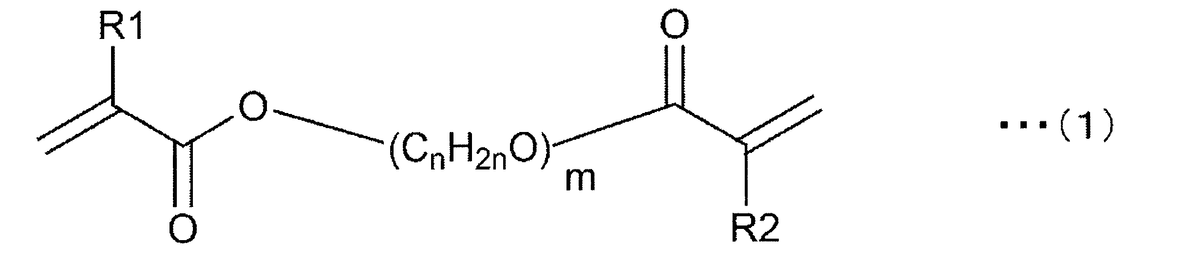
- a carboxyl group-containing resin a first acrylic monomer having three or more (meth) acryloyl groups, a second acrylic monomer represented by the following formula (1), and photopolymerization
- a curable composition includes an initiator and titanium oxide.
- R1 and R2 each represent a hydrogen atom or a methyl group
- n represents an integer of 1 to 6
- m represents an integer of 1 to 30.
- the curable composition contains an epoxy compound.
- the epoxy compound is solid at 25 ° C.
- a ratio of the content of the first acrylic monomer to the content of the second acrylic monomer is 0.05 or more and 20 or less on a weight basis. is there.
- the curable composition is a developable resist curable composition used for forming a resist film by a development process.
- a step of applying the curable composition described above on the surface of an electronic component main body to form a composition layer, and irradiating the composition layer with light to form a cured coating And a method for producing an electronic component, wherein the composition layer is developed to form the cured film.
- the composition layer is a resist layer
- the cured film is a resist film
- the curable composition according to the present invention includes a carboxyl group-containing resin, a first acrylic monomer having three or more (meth) acryloyl groups, a second acrylic monomer represented by formula (1), and photopolymerization. Since it contains an initiator and titanium oxide, discoloration when the cured product is exposed to high temperature can be suppressed.
- FIGS. 1A to 1E are cross-sectional views for explaining an example of a method for producing an electronic component using a curable composition according to an embodiment of the present invention.
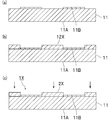
- 2 (a) to 2 (c) are cross-sectional views for explaining another example of a method for producing an electronic component using the curable composition according to one embodiment of the present invention.
- the curable composition according to the present invention is preferably used after being cured by light irradiation.
- the curable composition according to the present invention is preferably used for forming a cured film by development processing, and more preferably used for forming a resist film by development processing.
- the curable composition according to the present invention is preferably a developable resist curable composition.
- development may not be performed to form a resist film, and the curable composition according to the present invention may be a non-developable resist curable composition.
- the curable composition according to the present invention is preferably a curable composition for solder resist.
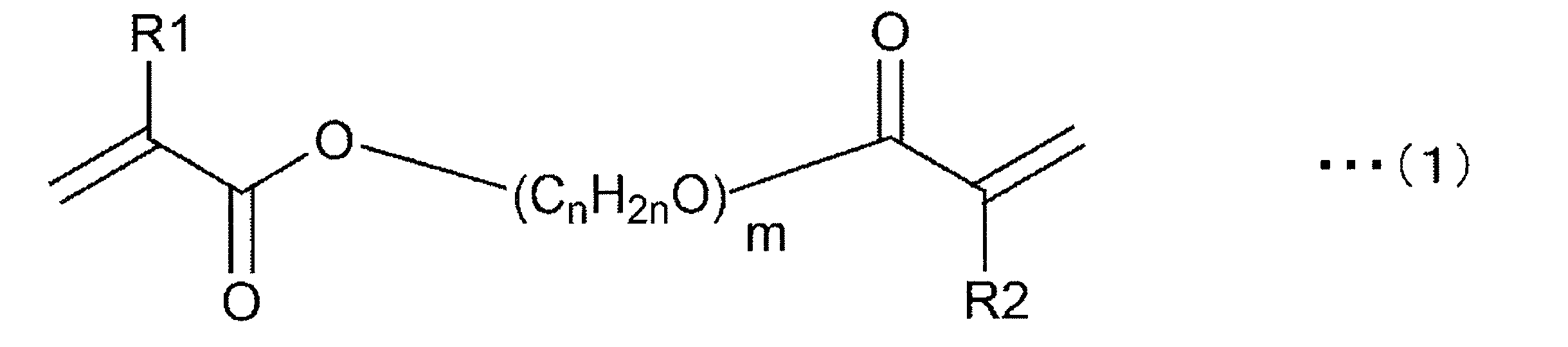
- the curable composition according to the present invention is represented by (A) a carboxyl group-containing resin, (B) a first acrylic monomer having three or more (meth) acryloyl groups, and (C) the following formula (1).
- R1 and R2 each represent a hydrogen atom or a methyl group
- n represents an integer of 1 to 6
- m represents an integer of 1 to 30.
- a specific (B) first acrylic monomer and (C) a second acrylic monomer are used in combination.
- C) In the second acrylic monomer two (meth) acryloyl groups are directly bonded to the —O— (C n H 2n O) m group without other groups.
- the (C) second acrylic monomer only the —O— (C n H 2n O) m group exists between the two (meth) acryloyl groups, and no other group exists.
- two (meth) acryloyl groups are replaced with —O— (C n H 2n O) m groups and other groups.
- a second acrylic monomer that is directly bonded without intervening two (meth) acryloyl groups are indirectly bonded to —O— (C n H 2n O) m group via another group.
- discoloration can be suppressed effectively, especially heat-resistant yellowing can be improved effectively, and generation
- an —O— (C n H 2n O) m group is provided between two (meth) acryloyl groups.
- the carboxyl group-containing resin is preferably a polymerizable polymer having a carboxyl group.
- the polymerizable polymer having a carboxyl group has polymerizability and can be polymerized.
- a carboxyl group-containing resin is a resin other than an acrylic monomer having three or more (meth) acryloyl groups, and is a resin other than an acrylic monomer represented by formula (1).
- As for carboxyl group-containing resin only 1 type may be used and 2 or more types may be used together.
- the carboxyl group-containing resin has a carboxyl group, the developability of the curable composition is improved.
- the (A) carboxyl group-containing resin include an acrylic resin having a carboxyl group, an epoxy resin having a carboxyl group, and an olefin resin having a carboxyl group.
- the “resin” is not limited to a solid resin, and includes a liquid resin and an oligomer.
- the carboxyl group-containing resin is preferably the following carboxyl group-containing resins (a) to (e).
- (E) A resin obtained by reacting an epoxy compound having an aromatic ring with a saturated polybasic acid anhydride or an unsaturated polybasic acid anhydride, or an epoxy compound having an aromatic ring and at least one unsaturated double bond Resin obtained by further reacting with saturated polybasic acid anhydride or unsaturated polybasic acid anhydride after reacting with carboxyl group-containing compound
- the content of the (A) carboxyl group-containing resin is preferably 3% by weight or more, more preferably 5% by weight or more, preferably 50% by weight or less. More preferably, it is 40% by weight or less.
- the content of the carboxyl group-containing resin is not less than the above lower limit and not more than the above upper limit, the curability, photosensitivity, and developability of the curable composition are improved, and the residue is further reduced after development.
- 100% by weight of all components excluding the solvent of the curable composition means 100% by weight of all components of the curable composition excluding the solvent, and the curable composition is the solvent. When it is not included, it means 100% by weight of the curable composition.
- the first acrylic monomer has three or more (meth) acryloyl groups.
- the number of (meth) acryloyl groups in the first acrylic monomer may be 6 or less, or 5 or less.
- As for the 1st acrylic monomer only 1 type may be used and 2 or more types may be used together.
- Examples of the polyhydric alcohol include hexanediol, trimethylolpropane, pentaerythritol, dipentaerythritol, and tris-hydroxyethyl isocyanurate.
- Examples of the (meth) acrylate of phenol include phenoxy (meth) acrylate and di (meth) acrylate modified products of bisphenol A.
- (Meth) acryloyl means acryloyl and methacryloyl.
- (Meth) acryl means acrylic and methacrylic.
- (Meth) acrylate means acrylate and methacrylate.
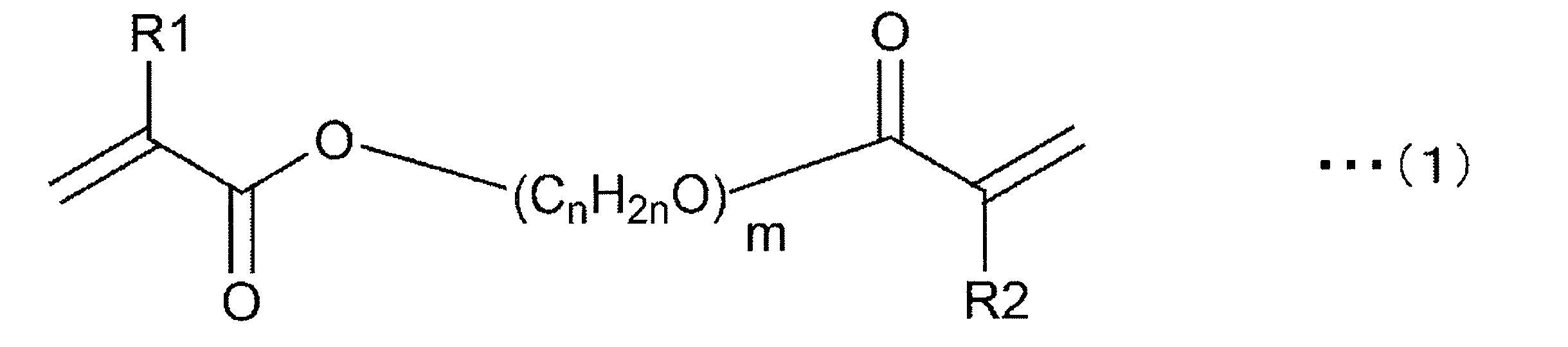
- the second acrylic monomer is represented by the following formula (1).
- R1 and R2 each represent a hydrogen atom or a methyl group
- n represents an integer of 1 to 6
- m represents an integer of 1 to 30.
- n is preferably an integer of 4 or less, more preferably an integer of 3 or less, and even more preferably 1 or 2.
- m is preferably an integer of 1 or more, preferably an integer of 25 or less, more preferably an integer of 20 or less, and even more preferably an integer of 15 or less. Particularly preferably, it is an integer of 10 or less.
- the second acrylic monomer is preferably a di (meth) acrylate modified product of alkylene glycol.
- the total content of (B) the first acrylic monomer and (C) the second acrylic monomer is preferably 3% by weight or more, more preferably Is 5% by weight or more, preferably 50% by weight or less, more preferably 40% by weight or less.
- the total content of (B) the first acrylic monomer and (C) the second acrylic monomer is not less than the above lower limit and not more than the above upper limit, discoloration of the cured product at a high temperature is further suppressed, and development There will be less residue later.
- Ratio of content of first acrylic monomer to content of (C) second acrylic monomer ((B) content of first acrylic monomer / (C) content of second acrylic monomer) Is preferably 0.05 or more, more preferably 1 or more, preferably 20 or less, more preferably 5 or less on a weight basis. (B) When the content of the first acrylic monomer is increased, the photocurability is further improved. (C) When the content of the second acrylic monomer is increased, the residue after development is further decreased.
- (D) Photopolymerization initiator Since the curable composition contains (D) a photopolymerization initiator, the curable composition can be cured by light irradiation. (D) As for a photoinitiator, only 1 type may be used and 2 or more types may be used together.
- the photopolymerization initiator for example, acylphosphine oxide, halomethylated triazine, halomethylated oxadiazole, imidazole, benzoin, benzoin alkyl ether, anthraquinone, benzanthrone, benzophenone, acetophenone, thioxanthone, benzoate, Examples include acridine, phenazine, titanocene, ⁇ -aminoalkylphenone, oxime, and derivatives thereof.
- an acylphosphine oxide photopolymerization initiator is preferable.
- the content is preferably 0.1 parts by weight or more, more preferably 1 part by weight or more, preferably 30 parts by weight or less, more preferably 15 parts by weight or less.
- content of a photoinitiator is more than the said minimum and below the said upper limit, the photosensitivity and sclerosis
- the titanium oxide is preferably rutile type titanium oxide or anatase type titanium oxide, and more preferably rutile type titanium oxide.
- the use of rutile type titanium oxide further suppresses discoloration of the cured product at high temperatures.
- the anatase type titanium oxide has a lower hardness than the rutile type titanium oxide. For this reason, use of anatase-type titanium oxide further increases the workability of the cured product.
- titanium oxide examples include sulfuric acid method titanium oxide and chlorine method titanium oxide. From the viewpoint of further suppressing discoloration of the cured product at a high temperature, chlorine-based titanium oxide is preferable. Chlorine titanium oxide is titanium oxide produced by the chlorine method.
- (E) titanium oxide is preferably rutile titanium oxide.
- the titanium oxide includes rutile type titanium oxide which is a surface treatment product of silicon oxide or silicone compound.
- the content of rutile-type titanium oxide, which is a surface-treated product of the above silicon oxide or silicone compound is preferably 10% by weight or more, more preferably 30% by weight or more, preferably 100% by weight. % Or less.
- the total amount of titanium oxide may be rutile titanium oxide which is a surface-treated product of the above silicon oxide or silicone compound.
- Examples of the rutile-type titanium oxide that is a surface-treated product of silicon oxide or silicone compound include, for example, a product number: CR-90 manufactured by Ishihara Sangyo Co., Ltd., which is a rutile chlorine method titanium oxide, and Ishihara Sangyo Co., Ltd., a rutile sulfuric acid method titanium oxide Product number: R-550, etc.
- the average particle diameter of titanium oxide is preferably 0.1 ⁇ m or more, more preferably 0.15 ⁇ m or more, preferably 1 ⁇ m or less, more preferably 0.5 ⁇ m or less.
- the average particle diameter in titanium oxide is a particle diameter value when the integrated value is 50% in the volume-based particle size distribution curve.
- the average particle size can be measured using, for example, a laser beam type particle size distribution meter. Examples of commercially available laser beam particle size distribution analyzers include “LS 13 320” manufactured by Beckman Coulter.
- the content of (E) titanium oxide is preferably 3% by weight or more, more preferably 10% by weight or more, still more preferably 15% by weight or more, preferably 80% by weight or less, more preferably 75% by weight or less, and still more preferably 70% by weight or less.
- the content of titanium oxide is not less than the above lower limit and not more than the above upper limit, discoloration of the cured product at a high temperature can be further suppressed. Furthermore, a curable composition having a viscosity suitable for coating can be easily prepared.
- the said curable composition may contain the inorganic filler different from (F) titanium oxide.
- the inorganic filler is an inorganic filler different from titanium oxide.
- As for an inorganic filler only 1 type may be used and 2 or more types may be used together.
- the inorganic filler examples include silica, alumina, mica, beryllia, potassium titanate, barium titanate, strontium titanate, calcium titanate, zirconium oxide, antimony oxide, aluminum borate, aluminum hydroxide, oxidation Magnesium, calcium carbonate, magnesium carbonate, aluminum carbonate, calcium silicate, aluminum silicate, magnesium silicate, calcium phosphate, calcium sulfate, barium sulfate, silicon nitride, boron nitride, clays such as calcined clay, talc, silicon carbide, crosslinked acrylic Resin particles, silicone particles, and the like.
- the curable composition contains talc or silica. It is preferable to include, and it is more preferable to include silica.
- the curable composition may contain talc.
- the average particle diameter of the inorganic filler is preferably 0.1 ⁇ m or more, more preferably 0.2 ⁇ m or more, preferably 10 ⁇ m or less, more preferably 5 ⁇ m or less.
- the average particle diameter in the inorganic filler is a particle diameter value when the integrated value is 50% in the volume-based particle size distribution curve.
- the average particle size can be measured using, for example, a laser beam type particle size distribution meter. Examples of commercially available laser beam particle size distribution analyzers include “LS 13 320” manufactured by Beckman Coulter.
- the content of the (F) inorganic filler is preferably 0.1% by weight or more, more preferably 1% by weight or more, still more preferably 3% by weight or more, preferably 50% by weight. Hereinafter, it is more preferably 30% by weight or less, and further preferably 10% by weight or less.
- the content of the inorganic filler is not less than the above lower limit and not more than the above upper limit, discoloration of the cured product at a high temperature is further suppressed, the light resistance of the cured product is further increased, and the surface of the cured product is improved. Stickiness is further suppressed.
- the total content of (E) titanium oxide and (F) inorganic filler is preferably 5% by weight or more, more preferably 10% by weight or more, and still more preferably 20% by weight. % Or more, preferably 80% by weight or less, more preferably 60% by weight or less, and still more preferably 40% by weight or less.
- the total content of (E) titanium oxide and (F) inorganic filler is not less than the above lower limit and not more than the above upper limit, discoloration of the cured product at a high temperature is further suppressed, and the light resistance of the cured product is further improved. It becomes higher and the stickiness of the surface of the cured product is further suppressed.
- the ratio of (E) titanium oxide content to (F) inorganic filler content is based on weight. , Preferably 0.1 or more, more preferably 1 or more, preferably 50 or less, more preferably 30 or less.
- the curable composition preferably contains (G) an epoxy compound for the purpose of improving the cutout processability of the cured product. Moreover, the curability of the curable composition is improved by using the (G) epoxy compound.
- the epoxy compound is an epoxy compound other than (A) a carboxyl group-containing resin.
- As for an epoxy compound only 1 type may be used and 2 or more types may be used together.
- Examples of the epoxy compound include heterocyclic epoxy resins such as bisphenol S type epoxy resin, diglycidyl phthalate resin, triglycidyl isocyanurate, bixylenol type epoxy resin, biphenol type epoxy resin, tetraglycidyl xylenoyl ethane.
- heterocyclic epoxy resins such as bisphenol S type epoxy resin, diglycidyl phthalate resin, triglycidyl isocyanurate, bixylenol type epoxy resin, biphenol type epoxy resin, tetraglycidyl xylenoyl ethane.
- Resin bisphenol A type epoxy resin, hydrogenated bisphenol A type epoxy resin, bisphenol F type resin, brominated bisphenol A type epoxy resin, phenol novolac type epoxy resin, cresol novolac type epoxy resin, alicyclic epoxy resin, bisphenol A Novolac epoxy resin, chelate epoxy resin, glyoxal epoxy resin, amino group-containing epoxy resin, rubber-modified epoxy resin, dicyclopentadiene phenolic epoxy Fat, and silicone-modified epoxy resin and ⁇ - caprolactone-modified epoxy resin.
- G As for an epoxy compound, only 1 type may be used and 2 or more types may be used together.
- the epoxy compound preferably reacts with the carboxyl group of the (A) carboxyl group-containing resin to act to cure the curable composition.
- the (G) epoxy compound is preferably not liquid at 25 ° C., and is solid at 25 ° C. Preferably there is.
- the epoxy compound is not liquid at 25 ° C.
- the epoxy resin to be tested is crystallized, the epoxy resin to be tested is kept at a temperature of 80 ° C for 24 hours and then within 0.5 hours. It means that the test sample is cooled to 25 ° C. and the elapsed time after reaching 25 ° C. is within one hour, satisfying either of the following two conditions.
- a test sample is placed in a vertical test tube (made of flat bottom cylindrical glass having an inner diameter of 30 mm and a height of 120 mm) until the height from the bottom of the test tube reaches 55 mm.
- a vertical test tube made of flat bottom cylindrical glass having an inner diameter of 30 mm and a height of 120 mm
- the distance between the tip of the moving surface of the test sample and the bottom of the test tube is 60
- the time until it passes through the millimeter portion is 90 seconds or more, it is determined as “not liquid at 25 ° C.”.
- test sample When the test sample is measured with a B-type viscometer under the condition of 25 ° C. and is 3,000,000 centipoise or more, it is regarded as “not liquid at 25 ° C.”
- the content of the (G) epoxy compound is preferably 0.1 parts by weight or more, more preferably 1 part by weight or more, preferably 50 parts per 100 parts by weight of the (A) carboxyl group-containing resin. It is 30 parts by weight or less, more preferably 30 parts by weight or less.
- cured material becomes it still higher that content of an epoxy compound is more than the said minimum and below the said upper limit.
- the curable composition may contain (H) a solvent.
- (H) As for a solvent only 1 type may be used and 2 or more types may be used together.
- the solvent is generally an organic solvent.
- the organic solvent include ketone compounds such as methyl ethyl ketone and cyclohexanone, aromatic hydrocarbon compounds such as toluene, xylene, and tetramethylbenzene, cellosolve, methyl cellosolve, butyl cellosolve, carbitol, methyl carbitol, butyl carbitol, and propylene glycol monomethyl.
- Glycol ether compounds such as ether, dipropylene glycol monomethyl ether, dipropylene glycol diethyl ether, tripropylene glycol monomethyl ether, ethyl acetate, butyl acetate, butyl lactate, cellosolve acetate, butyl cellosolve acetate, carbitol acetate, butyl carbitol acetate, propylene Glycol monomethyl ether acetate, diethylene glycol monoethyl ether Seteto, dipropylene glycol monomethyl ether acetate, ester compounds such as propylene carbonate, octane, aliphatic hydrocarbon compounds decane, petroleum ether, petroleum solvent and dibasic ester such as naphtha.
- the dibasic acid ester is a solvent called DBE.
- the content of the (H) solvent is preferably 5% by weight or more, more preferably 10% by weight or more, preferably 50% by weight or less, more preferably 30% by weight or less.
- the curable composition may contain (I) an antioxidant.
- the antioxidant preferably has a Lewis basic moiety.
- the antioxidant is preferably a phenolic antioxidant, a phosphorus antioxidant, or an amine antioxidant. More preferably, it is an inhibitor.
- IRGANOX 1010 Commercially available products of the above-mentioned phenolic antioxidants include IRGANOX 1010, IRGANOX 1035, IRGANOX 1076, IRGANOX 1135, IRGANOX 245, IRGANOX 259, and IRGANOX 295 (all of which are manufactured by Ciba Japan), ADK STAB AO-30, ADK STAB AO-40, ADK STAB AO-50, ADK STAB AO-60, ADK STAB AO-70, ADK STAB AO-80, ADK STAB AO-90, and ADK STAB AO-330 (all of which are manufactured by ADEKA), Sumilizer GA-80, and Sumizer MDP-S, Sumilizer BBM-S, Sumilizer GM, Sumilizer GS (F), and S milizer GP (all of which are manufactured by Sumitomo Chemical Co., Ltd.), HOSTANOX O10, HOSTANOX O16, HOSTANO
- Examples of the phosphorus antioxidant include cyclohexylphosphine and triphenylphosphine.
- Commercially available phosphoric antioxidants include ADK STAB PEP-4C, ADK STAB PEP-8, ADK STAB PEP-24G, ADK STAB PEP-36, ADK STAB HP-10, ADK STAB 2112, ADK STAB 260, ADK STAB 522A, ADK STAB 1178, ADK STAB 1178, and ADK STAB 1178 1500, ADK STAB C, ADK STAB 135A, ADK STAB 3010, and ADK STAB TPP (all manufactured by ADEKA), Sandstub P-EPQ, and Hostanox PAR24 (all manufactured by Clariant), and JP-312L, JP -318-0, JPM-308, JPM-313, JPP-613M, JPP-31, JPP-2000PT, and JPH-3800 Re also be mentioned Johoku Chemical Industry Co., Ltd.), and the like.
- amine antioxidant examples include triethylamine, dicyandiamide, melamine, ethyldiamino-S-triazine, 2,4-diamino-S-triazine, 2,4-diamino-6-tolyl-S-triazine, 2,4- And diamino-6-xylyl-S-triazine and quaternary ammonium salt derivatives.
- the content of (I) antioxidant is preferably 0.1 parts by weight or more, more preferably 5 parts by weight or more, preferably 30 parts by weight or less, more preferably 100 parts by weight of the carboxyl group-containing resin. Is 15 parts by weight or less.
- the curable composition includes a colorant, a filler, an antifoaming agent, a curing agent, a curing accelerator, a release agent, a surface treatment agent, a flame retardant, a viscosity modifier, a dispersant, a dispersion aid, and a surface modifier.
- Plasticizers, antibacterial agents, antifungal agents, leveling agents, stabilizers, coupling agents, anti-sagging agents or phosphors may be included.
- the above-mentioned curable composition can be prepared, for example, by stirring and mixing each compounding component and then uniformly mixing with three rolls.
- Examples of the light source used for curing the curable composition include an irradiation device that emits active energy rays such as ultraviolet rays or visible rays.
- Examples of the light source include an ultrahigh pressure mercury lamp, a deep UV lamp, a high pressure mercury lamp, a low pressure mercury lamp, a metal halide lamp, and an excimer laser. These light sources are appropriately selected according to the photosensitive wavelength of the constituent components of the curable composition.
- the irradiation energy of light is appropriately selected depending on the desired thickness or the constituent components of the curable composition.
- the irradiation energy of light is generally in the range of 10 to 3000 mJ / cm 2 .
- the method of manufacturing an electronic component according to the present invention includes a step of coating the curable composition on the surface of the electronic component body to form a composition layer, and irradiating the composition layer with light to cure. Forming a film.
- the composition layer may be developed in order to form the cured film.
- the composition layer is preferably a resist layer, and the cured film is preferably a resist film.
- the photocurable composition can be applied partially and at a plurality of locations on the surface of the electronic component body.
- the composition layer is not thermally cured by the action of a thermosetting agent in order to form the cured film. From the viewpoint of preventing thermal deterioration of the electronic component body, it is preferable not to heat to 150 ° C. or higher, and more preferably not to heat to 100 ° C. or higher, in order to form the cured film.
- the composition layer is a resist layer
- the cured film is a resist film.
- a non-developing resist photocurable composition is used.
- 1 (a) to 1 (e) are cross-sectional views for explaining an example of a method for producing an electronic component using the curable composition according to one embodiment of the present invention.
- an application target member 11 is prepared.
- the application target member 11 is an electronic component main body.
- a substrate 11A is used as the application target member 11, and a plurality of electrodes 11B are arranged on the surface of the substrate 11A.
- a resist layer 12 (composition layer) is formed.
- a resist layer 12 is formed on the entire surface of the application target member 11.
- FIG. 1C only the resist layer 12 between the electrodes 11B is irradiated with light through a mask 13.
- FIG. 1D development is performed, and the resist layer 12 located on the electrode 11B and not irradiated with light is partially removed.
- the remaining resist layer 12 is thermally cured.
- FIG. 1E the electronic component 1 in which the resist film 2 is formed on the surface of the application target member 11 (electronic component main body) is obtained.
- FIGS. 2A to 2C are cross-sectional views for explaining another example of a method for manufacturing an electronic component using the curable composition according to one embodiment of the present invention.
- the application target member 11 is prepared.
- a curable composition (used as a non-developing resist curable composition) according to the second embodiment of the present invention is applied on the surface of the application target member 11.
- a resist layer 12X (composition layer) is formed.
- the said curable composition is apply
- a plurality of resist layers 12X are formed between the plurality of electrodes 11B on the surface of the substrate 11A.
- the resist layer 12X is, for example, a resist pattern.
- the resist layer 12X is formed only at a position corresponding to a resist layer portion that is formed to remain after development when it is assumed that a development-type resist curable composition is used.
- the resist layer 12X is not formed at a position corresponding to the resist layer portion to be removed by development using a development-type resist curable composition.
- the resist layer 12X is irradiated with light.
- the resist layer 12X is irradiated with light from the side opposite to the application target member 11 side of the resist layer 12X.
- the resist layer 12X is photocured to form a resist film 2X (cured film).
- the electronic component 1X in which the resist film 2X is formed on the surface of the application target member 11 is obtained.
- Examples of the coating method of the curable composition include a coating method using a dispenser, a coating method using screen printing, and a coating method using an inkjet device. Screen printing is preferred because of its excellent manufacturing efficiency. It is preferable to pattern-print the curable composition.
- each time one layer of the photocurable composition is applied to the surface of the application target member light may be irradiated to form a hand-cured product layer (resist layer or the like), or two or more layers are applied. You may irradiate light later and may form a hardened
- Glycidyl acrylate was added in such an amount that the molar ratio of the total amount of all the monomer units of the obtained resin was 10 and then heated at 100 ° C. for 30 hours using tetrabutylammonium bromide as a catalyst. The group was subjected to an addition reaction. After cooling, it was taken out from the flask to obtain a solution containing 50 wt% (nonvolatile content) of a carboxyl group-containing resin having a solid content acid value of 60 mg KOH / g, a weight average molecular weight of 15000, and a double bond equivalent of 1000.
- this solution is referred to as acrylic polymer 1.
- DPHA first acrylic monomer, dipentaerythritol hexaacrylate, manufactured by Daicel Ornex
- TMPTA first acrylic monomer, trimethylolpropane triacrylate, manufactured by Daicel Ornex
- A-200 second acrylic monomer, polyethylene glycol diacrylate, manufactured by Shin-Nakamura Chemical Co., Ltd.
- A-400 second acrylic monomer, polyethylene glycol diacrylate, manufactured by Shin-Nakamura Chemical Co., Ltd.
- A-600 (second acrylic monomer, polyethylene glycol diacrylate, manufactured by Shin-Nakamura Chemical Co., Ltd.)
- A-1000 second acrylic monomer, polyethylene glycol diacrylate, manufactured by Shin-Nakamura Chemical Co., Ltd.
- APG-400 second acrylic monomer, polypropylene glycol diacrylate, manufactured by Shin-Nakamura Chemical Co., Ltd.
- A-PTMG-65 (second acrylic monomer, polytetramethylene glycol diacrylate, manufactured by Shin-Nakamura Chemical Co., Ltd.)
- BPE-1300N other acrylic monomer, ethoxylated bisphenol A dimethacrylate, manufactured by Shin-Nakamura Chemical Co., Ltd.
- ABE-300 other acrylic monomer, ethoxylated bisphenol A diacrylate, manufactured by Shin-Nakamura Chemical Co., Ltd.
- jER828 bisphenol A type epoxy resin, manufactured by Mitsubishi Chemical Corporation, liquid at 25 ° C.
- TPO photopolymerization initiator which is a photo radical generator, manufactured by BASF Japan
- CR-50 titanium oxide, manufactured by Ishihara Sangyo Co., Ltd.
- KS-7710 compound type silicone oil, polydimethylsiloxane, manufactured by Shin-Etsu Chemical Co., Ltd.
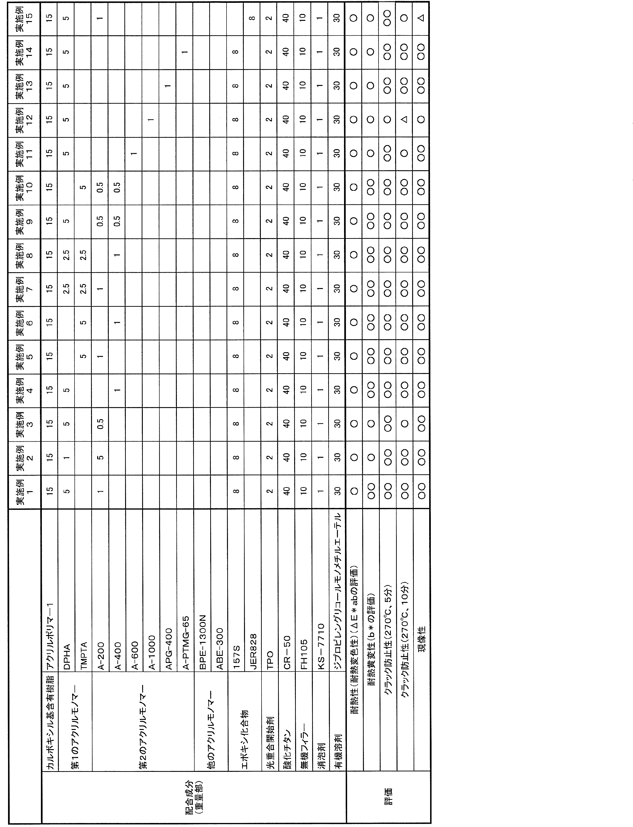
- Example 1 15 parts by weight of the acrylic polymer 1 obtained in Synthesis Example 1, 5 parts by weight of DPHA (first acrylic monomer, dipentaerythritol hexaacrylate, manufactured by Daicel Ornex), and A-200 (second acrylic monomer) , Polyethylene glycol diacrylate (manufactured by Shin-Nakamura Chemical Co., Ltd.) 1 part by weight, 157S (bisphenol A novolac type epoxy resin, manufactured by Mitsubishi Chemical Corporation, solid at 25 ° C.) 8 parts by weight, and TPO (photo radical generator) 2 parts by weight of a photopolymerization initiator (BASF Japan), 40 parts by weight of CR-50 (titanium oxide, manufactured by Ishihara Sangyo), 10 parts by weight of FH105 (talc, manufactured by Fuji Talc), and KS-7710 ( (Compound type silicone oil, polydimethylsiloxane, manufactured by Shin-Etsu Chemical Co., Ltd.) 1 part by weight, dipropylene glycol
- Examples 2 to 15 and Comparative Examples 1 to 5 A resist material, which is a curable composition, was obtained in the same manner as in Example 1 except that the type and blending amount of the material used were changed as shown in Tables 1 and 2 below.
- the resist material layer is immersed in a 1 wt% aqueous solution of sodium carbonate (25 ° C.) for 30 seconds and developed, and a resist film is formed on the substrate. Formed. Thereafter, the resist film was post-cured by heating in an oven at 150 ° C. for 1 hour to obtain a resist film as a measurement sample. The thickness of the obtained resist film was 20 ⁇ m.
Landscapes
- Chemical & Material Sciences (AREA)
- Physics & Mathematics (AREA)
- Organic Chemistry (AREA)
- Health & Medical Sciences (AREA)
- Chemical Kinetics & Catalysis (AREA)
- Medicinal Chemistry (AREA)
- Polymers & Plastics (AREA)
- General Physics & Mathematics (AREA)
- Spectroscopy & Molecular Physics (AREA)
- Materials For Photolithography (AREA)
- Polymerisation Methods In General (AREA)
- Epoxy Resins (AREA)
- Macromonomer-Based Addition Polymer (AREA)
- Non-Metallic Protective Coatings For Printed Circuits (AREA)
- Compositions Of Macromolecular Compounds (AREA)
- Graft Or Block Polymers (AREA)
- Addition Polymer Or Copolymer, Post-Treatments, Or Chemical Modifications (AREA)
Abstract
Description
本発明に係る硬化性組成物は、光の照射により硬化されて用いられることが好ましい。本発明に係る硬化性組成物は、現像処理により硬化被膜を形成するために用いられることが好ましく、現像処理によりレジスト膜を形成するために用いられることがより好ましい。本発明に係る硬化性組成物は、現像型レジスト硬化性組成物であることが好ましい。本発明に係る硬化性組成物においては、レジスト膜を形成するために現像が行われなくてもよく、本発明に係る硬化性組成物は、非現像型レジスト硬化性組成物であってもよい。本発明に係る硬化性組成物は、ソルダーレジスト用硬化性組成物であることが好ましい。
(A)カルボキシル基含有樹脂は、カルボキシル基を有する重合性重合体であることが好ましい。カルボキシル基を有する重合性重合体は、重合性を有し、重合可能である。(A)カルボキシル基含有樹脂は、(メタ)アクリロイル基を3つ以上有するアクリルモノマー以外の樹脂であり、式(1)で表されるアクリルモノマー以外の樹脂である。(A)カルボキシル基含有樹脂は、1種のみが用いられてもよく、2種以上が併用されてもよい。
(B)第1のアクリルモノマーは、(メタ)アクリロイル基を3つ以上有する。(B)第1のアクリルモノマーの(メタ)アクリロイル基の数は6以下であってもよく、5以下であってもよい。(B)第1のアクリルモノマーは、1種のみが用いられてもよく、2種以上が併用されてもよい。
上記硬化性組成物は、(D)光重合開始剤を含むので、光の照射により硬化性組成物を硬化させることができる。(D)光重合開始剤は、1種のみが用いられてもよく、2種以上が併用されてもよい。
上記硬化性組成物が(E)酸化チタンを含むので、反射率が高いレジスト膜などの硬化物を形成できる。(E)酸化チタンを用いることによって、(E)酸化チタン以外の他の無機フィラーを用いた場合と比較して、反射率が高い硬化物を形成できる。(E)酸化チタンは、1種のみが用いられてもよく、2種以上が併用されてもよい。
上記硬化性組成物は、(F)酸化チタンとは異なる無機フィラーを含んでいてもよい。(F)無機フィラーは、酸化チタンとは異なる無機フィラーである。(F)無機フィラーは1種のみが用いられてもよく、2種以上が併用されてもよい。
硬化物の切り出し加工性を高めることなどを目的として、上記硬化性組成物は、(G)エポキシ化合物を含むことが好ましい。また、(G)エポキシ化合物の使用により、硬化性組成物の硬化性も良好になる。(G)エポキシ化合物は、(A)カルボキシル基含有樹脂以外のエポキシ化合物である。(G)エポキシ化合物は、1種のみが用いられてもよく、2種以上が併用されてもよい。
上記硬化性組成物は、(H)溶剤を含んでいてもよい。(H)溶剤は、1種のみが用いられてもよく、2種以上が併用されてもよい。
硬化物の高温下での変色をより一層抑える観点からは、上記硬化性組成物は、(I)酸化防止剤を含んでいてもよい。(I)酸化防止剤は、ルイス塩基性部位を有することが好ましい。硬化物の高温下での変色をより一層抑える観点からは、(I)酸化防止剤は、フェノール系酸化防止剤、リン系酸化防止剤又はアミン系酸化防止剤であることが好ましく、フェノール系酸化防止剤であることがより好ましい。
上記硬化性組成物は、着色剤、充填剤、消泡剤、硬化剤、硬化促進剤、離型剤、表面処理剤、難燃剤、粘度調節剤、分散剤、分散助剤、表面改質剤、可塑剤、抗菌剤、防黴剤、レベリング剤、安定剤、カップリング剤、タレ防止剤又は蛍光体等を含んでいてもよい。
本発明に係る電子部品の製造方法は、電子部品本体の表面上に、上記硬化性組成物を塗布して、組成物層を形成する工程と、上記組成物層に光を照射して、硬化被膜形成する工程とを備える。本発明に係る電子部品の製造方法では、上記硬化被膜を形成するために、上記組成物層を現像してもよい。上記組成物層がレジスト層であることが好ましく、上記硬化被膜がレジスト膜であることが好ましい。
(合成例1)
温度計、攪拌機、滴下ロート及び還流冷却器を備えたフラスコに、溶剤であるエチルカルビトールアセテートと、触媒であるアゾビスイソブチロニトリルとを入れ、窒素雰囲気下で80℃に加熱し、メタクリル酸とメチルメタクリレートとを30:70のモル比で混合したモノマーを2時間かけて滴下した。滴下後、1時間攪拌し、温度を120℃に上げた。その後、冷却した。得られた樹脂の全てのモノマー単位の総量のモル量に対するモル比が10となる量のグリシジルアクリレートを加え、触媒として臭化テトラブチルアンモニウムを用い100℃で30時間加熱して、グリシジルアクリレートとカルボキシル基とを付加反応させた。冷却後、フラスコから取り出して、固形分酸価60mgKOH/g、重量平均分子量15000、二重結合当量1000のカルボキシル基含有樹脂を50重量%(不揮発分)含む溶液を得た。以下、この溶液をアクリルポリマー1と呼ぶ。
、新中村化学工業社製)
合成例1で得られたアクリルポリマー1を15重量部と、DPHA(第1のアクリルモノマー、ジペンタエリスリトールヘキサアクリレート、ダイセル・オルネクス社製)5重量部と、A-200(第2のアクリルモノマー、ポリエチレングリコールジアクリレート、新中村化学工業社製)1重量部と、157S(ビスフェノールAノボラック型エポキシ樹脂、三菱化学社製、25℃で固体)8重量部と、TPO(光ラジカル発生剤である光重合開始剤、BASFジャパン社製)2重量部と、CR-50(酸化チタン、石原産業社製)40重量部と、FH105(タルク、富士タルク社製)10重量部と、KS-7710(コンパウンド型シリコーンオイル、ポリジメチルシロキサン、信越化学工業社製)1重量部と、ジプロピレングリコールモノメチルエーテル(MFDG、溶剤、日本乳化剤社製)30重量部とを配合し、混合機(シンキー社製「練太郎ARE-310」)にて3分間混合した後、3本ロールにて混合し、混合物を得た。その後、ARE-310を用いて、得られた混合物を3分間脱泡することにより、硬化性組成物であるレジスト材料を得た。
使用した材料の種類及び配合量を下記の表1,2に示すように変更したこと以外は、実施例1と同様にして、硬化性組成物であるレジスト材料を得た。
(1)測定サンプルの作製
80mm×90mm、厚さ0.8mmのFR-4基板を用意した。この基板上に、スクリーン印刷法により、100メッシュのポリエステルバイアス製の版を用いて、ベタパターンでレジスト材料を印刷した。印刷後、80℃のオーブン内で20分間乾燥させ、レジスト材料層を基板上に形成した。次に、所定のパターンを有するフォトマスクを介して、紫外線照射装置を用い、レジスト材料層に波長365nmの紫外線を、照射エネルギーが400mJ/cm2となるように100mW/cm2の紫外線照度で4秒間照射した。その後、未露光部のレジスト材料層を除去してパターンを形成するために、炭酸ナトリウムの1重量%水溶液(25℃)にレジスト材料層を30秒間浸漬して現像し、基板上にレジスト膜を形成した。その後、150℃のオーブン内で1時間加熱しレジスト膜を後硬化させることにより、測定サンプルとしてのレジスト膜を得た。得られたレジスト膜の厚みは20μmであった。
測定サンプルを加熱オーブン内に入れ、270℃で5分間加熱した。
○:ΔE*abが0.5以下
△:ΔE*abが0.5を超え、1以下
×:ΔE*abが1を超える
○○:b*の変化量が1.0下
○:b*が1.0を超え、1.5以下
△:b*が1.5を超え、2.0以下
×:b*が2.0を超える
測定サンプルを加熱オーブン内に入れ、270℃で5分間加熱した。270℃で5分間加熱した後の測定サンプルにおいて、レジスト膜におけるクラックの発生状態を確認した。また、測定サンプルを加熱オーブン内に入れ、270℃で10分間加熱した。270℃で10分間加熱した後の測定サンプルにおいて、レジスト膜におけるクラックの発生状態を確認した。
○○:クラックが発生していない
○:最大長さが500μm未満のわずかなクラックが発生している
△:最大長さが500μm以上、1000μm未満のクラックが発生している
×:最大長さが1000μm以上のクラックが発生している
測定サンプルの未露光部のレジスト残渣、即ちレジスト材料層が除去され、パターン形成された銅表面に残っているレジスト残渣を観察した。この残渣から、現像性を以下の基準で判定した。
○○:銅表面にレジスト材料層が全く残っておらず、銅色がはっきりと見える
○:銅表面にごくわずかにレジスト材料層が残っているが、銅色がはっきりと見える
△:銅表面にわずかにレジスト材料層が残っており、銅色が白くかすんでいる
×:銅表面にレジスト材料層が残っており、銅色が見えない

2,2X…レジスト膜
11…塗布対象部材(電子部品本体)
11A…基板
11B…電極
12,12X…レジスト層
13…マスク
Claims (7)
- カルボキシル基含有樹脂と、
(メタ)アクリロイル基を3つ以上有する第1のアクリルモノマーと、
下記式(1)で表される第2のアクリルモノマーと、
光重合開始剤と、
酸化チタンとを含む、硬化性組成物。

- エポキシ化合物を含む、請求項1に記載の硬化性組成物。
- 前記エポキシ化合物が、25℃で固体状である、請求項2に記載の硬化性組成物。
- 前記第1のアクリルモノマーの含有量の前記第2のアクリルモノマーの含有量に対する比が、重量基準で、0.05以上、20以下である、請求項1~3のいずれか1項に記載の硬化性組成物。
- 現像処理によりレジスト膜を形成するために用いられる現像型レジスト硬化性組成物である、請求項1~4のいずれか1項に記載の硬化性組成物。
- 電子部品本体の表面上に、請求項1~5のいずれか1項に記載の硬化性組成物を塗布して、組成物層を形成する工程と、
前記組成物層に光を照射して、硬化被膜を形成する工程とを備え、
前記硬化被膜を形成するために、前記組成物層を現像する、電子部品の製造方法。 - 前記組成物層がレジスト層であり、前記硬化被膜がレジスト膜である、請求項6に記載の電子部品の製造方法。
Priority Applications (3)
| Application Number | Priority Date | Filing Date | Title |
|---|---|---|---|
| CN201680024029.0A CN107531815B (zh) | 2015-11-24 | 2016-11-24 | 固化性组合物及电子部件的制造方法 |
| JP2016570123A JP6145232B1 (ja) | 2015-11-24 | 2016-11-24 | 硬化性組成物及び電子部品の製造方法 |
| KR1020177028748A KR102639455B1 (ko) | 2015-11-24 | 2016-11-24 | 경화성 조성물 및 전자 부품의 제조 방법 |
Applications Claiming Priority (2)
| Application Number | Priority Date | Filing Date | Title |
|---|---|---|---|
| JP2015228779 | 2015-11-24 | ||
| JP2015-228779 | 2015-11-24 |
Publications (1)
| Publication Number | Publication Date |
|---|---|
| WO2017090680A1 true WO2017090680A1 (ja) | 2017-06-01 |
Family
ID=58764351
Family Applications (1)
| Application Number | Title | Priority Date | Filing Date |
|---|---|---|---|
| PCT/JP2016/084798 Ceased WO2017090680A1 (ja) | 2015-11-24 | 2016-11-24 | 硬化性組成物及び電子部品の製造方法 |
Country Status (5)
| Country | Link |
|---|---|
| JP (2) | JP6145232B1 (ja) |
| KR (1) | KR102639455B1 (ja) |
| CN (1) | CN107531815B (ja) |
| TW (1) | TWI724068B (ja) |
| WO (1) | WO2017090680A1 (ja) |
Cited By (7)
| Publication number | Priority date | Publication date | Assignee | Title |
|---|---|---|---|---|
| JP2019091855A (ja) * | 2017-11-16 | 2019-06-13 | 積水化学工業株式会社 | 非現像型レジスト硬化性組成物、プリント配線板及び電子部品の製造方法 |
| JP2019091854A (ja) * | 2017-11-16 | 2019-06-13 | 積水化学工業株式会社 | 非現像型レジスト光硬化性組成物及び電子部品の製造方法 |
| WO2019189186A1 (ja) * | 2018-03-30 | 2019-10-03 | 太陽インキ製造株式会社 | インクジェット印刷用硬化性組成物、その硬化物、及びその硬化物を有する電子部品 |
| JP2019178270A (ja) * | 2018-03-30 | 2019-10-17 | 太陽インキ製造株式会社 | 硬化性組成物、その硬化物およびこれを有する電子部品 |
| JP2019178260A (ja) * | 2018-03-30 | 2019-10-17 | 太陽インキ製造株式会社 | インクジェット印刷用硬化性組成物、その硬化物、及びその硬化物を有する電子部品 |
| JPWO2019017047A1 (ja) * | 2017-07-21 | 2020-05-28 | 積水化学工業株式会社 | 硬化性組成物、電子部品及び電子部品の製造方法 |
| JP2023162297A (ja) * | 2018-06-29 | 2023-11-08 | 三菱ケミカル株式会社 | 活性エネルギー線硬化性組成物及び積層体 |
Families Citing this family (1)
| Publication number | Priority date | Publication date | Assignee | Title |
|---|---|---|---|---|
| JP7839821B2 (ja) * | 2024-03-27 | 2026-04-02 | 株式会社タムラ製作所 | 感光性樹脂組成物、感光性樹脂組成物の光硬化物及び当該光硬化物を有するプリント配線板 |
Citations (2)
| Publication number | Priority date | Publication date | Assignee | Title |
|---|---|---|---|---|
| JP2012053254A (ja) * | 2010-09-01 | 2012-03-15 | Sekisui Chem Co Ltd | 光及び熱硬化性組成物、ソルダーレジスト組成物及びプリント配線板 |
| WO2015012228A1 (ja) * | 2013-07-25 | 2015-01-29 | 東レ株式会社 | タッチパネル用ネガ型感光性白色組成物、タッチパネル及びタッチパネルの製造方法 |
Family Cites Families (5)
| Publication number | Priority date | Publication date | Assignee | Title |
|---|---|---|---|---|
| JP5650460B2 (ja) * | 2010-08-18 | 2015-01-07 | 株式会社タムラ製作所 | 白色硬化性樹脂組成物 |
| JP2014114402A (ja) | 2012-12-11 | 2014-06-26 | Taiyo Ink Mfg Ltd | 光硬化性組成物および成型品 |
| JP6359814B2 (ja) | 2013-09-17 | 2018-07-18 | 太陽インキ製造株式会社 | 感光性樹脂組成物、ドライフィルム、硬化物およびプリント配線板 |
| KR102339967B1 (ko) * | 2013-11-06 | 2021-12-17 | 세키스이가가쿠 고교가부시키가이샤 | 경화물막의 제조 방법, 전자 부품의 제조 방법 및 전자 부품 |
| JP2015106160A (ja) | 2015-01-19 | 2015-06-08 | 太陽インキ製造株式会社 | 感光性樹脂組成物、ドライフィルム、硬化物およびプリント配線板 |
-
2016
- 2016-11-24 CN CN201680024029.0A patent/CN107531815B/zh active Active
- 2016-11-24 KR KR1020177028748A patent/KR102639455B1/ko active Active
- 2016-11-24 TW TW105138731A patent/TWI724068B/zh active
- 2016-11-24 JP JP2016570123A patent/JP6145232B1/ja active Active
- 2016-11-24 WO PCT/JP2016/084798 patent/WO2017090680A1/ja not_active Ceased
-
2017
- 2017-04-24 JP JP2017085177A patent/JP2017141472A/ja active Pending
Patent Citations (2)
| Publication number | Priority date | Publication date | Assignee | Title |
|---|---|---|---|---|
| JP2012053254A (ja) * | 2010-09-01 | 2012-03-15 | Sekisui Chem Co Ltd | 光及び熱硬化性組成物、ソルダーレジスト組成物及びプリント配線板 |
| WO2015012228A1 (ja) * | 2013-07-25 | 2015-01-29 | 東レ株式会社 | タッチパネル用ネガ型感光性白色組成物、タッチパネル及びタッチパネルの製造方法 |
Cited By (10)
| Publication number | Priority date | Publication date | Assignee | Title |
|---|---|---|---|---|
| JPWO2019017047A1 (ja) * | 2017-07-21 | 2020-05-28 | 積水化学工業株式会社 | 硬化性組成物、電子部品及び電子部品の製造方法 |
| JP2019091855A (ja) * | 2017-11-16 | 2019-06-13 | 積水化学工業株式会社 | 非現像型レジスト硬化性組成物、プリント配線板及び電子部品の製造方法 |
| JP2019091854A (ja) * | 2017-11-16 | 2019-06-13 | 積水化学工業株式会社 | 非現像型レジスト光硬化性組成物及び電子部品の製造方法 |
| WO2019189186A1 (ja) * | 2018-03-30 | 2019-10-03 | 太陽インキ製造株式会社 | インクジェット印刷用硬化性組成物、その硬化物、及びその硬化物を有する電子部品 |
| JP2019178270A (ja) * | 2018-03-30 | 2019-10-17 | 太陽インキ製造株式会社 | 硬化性組成物、その硬化物およびこれを有する電子部品 |
| JP2019178260A (ja) * | 2018-03-30 | 2019-10-17 | 太陽インキ製造株式会社 | インクジェット印刷用硬化性組成物、その硬化物、及びその硬化物を有する電子部品 |
| JP7362991B2 (ja) | 2018-03-30 | 2023-10-18 | 太陽ホールディングス株式会社 | インクジェット印刷用硬化性組成物、その硬化物、及びその硬化物を有する電子部品 |
| JP7362992B2 (ja) | 2018-03-30 | 2023-10-18 | 太陽ホールディングス株式会社 | 硬化性組成物、その硬化物およびこれを有する電子部品 |
| JP2023162297A (ja) * | 2018-06-29 | 2023-11-08 | 三菱ケミカル株式会社 | 活性エネルギー線硬化性組成物及び積層体 |
| JP7697498B2 (ja) | 2018-06-29 | 2025-06-24 | 三菱ケミカル株式会社 | 活性エネルギー線硬化性組成物及び積層体 |
Also Published As
| Publication number | Publication date |
|---|---|
| CN107531815A (zh) | 2018-01-02 |
| KR102639455B1 (ko) | 2024-02-23 |
| TW201734059A (zh) | 2017-10-01 |
| TWI724068B (zh) | 2021-04-11 |
| CN107531815B (zh) | 2021-05-11 |
| JPWO2017090680A1 (ja) | 2017-11-24 |
| JP6145232B1 (ja) | 2017-06-07 |
| JP2017141472A (ja) | 2017-08-17 |
| KR20180087137A (ko) | 2018-08-01 |
Similar Documents
| Publication | Publication Date | Title |
|---|---|---|
| JP6145232B1 (ja) | 硬化性組成物及び電子部品の製造方法 | |
| JP4891434B2 (ja) | 感光性組成物及びプリント配線板 | |
| JP4762374B1 (ja) | 感光性組成物及びプリント配線板 | |
| JP2012212039A (ja) | 感光性組成物及びプリント配線板 | |
| JP2010181825A (ja) | 感光性組成物 | |
| JP2011075787A (ja) | 感光性組成物 | |
| JP2012053254A (ja) | 光及び熱硬化性組成物、ソルダーレジスト組成物及びプリント配線板 | |
| JP2011059391A (ja) | 感光性組成物及びプリント配線板 | |
| JP4850313B1 (ja) | 2液混合型の第1,第2の液及びプリント配線板の製造方法 | |
| JP4991960B1 (ja) | 2液混合型の第1,第2の液及びプリント配線板の製造方法 | |
| JP2011248322A (ja) | 感光性組成物、ソルダーレジスト組成物及び基板 | |
| KR101250736B1 (ko) | 2액 혼합형의 제1, 제2 액 및 인쇄 배선판의 제조 방법 | |
| JP6618829B2 (ja) | 2液混合型の第1,第2の液及びプリント配線板の製造方法 | |
| JP2019191303A (ja) | 硬化性組成物、電子部品、電子部品の製造方法 | |
| JP2016136248A (ja) | 感光性組成物及びプリント配線板 | |
| KR102625987B1 (ko) | 2액 혼합형의 제1, 제2 액 및 프린트 배선판의 제조 방법 | |
| JP6947492B2 (ja) | 2液混合型の第1,第2の液及びプリント配線板の製造方法 | |
| CN106019828A (zh) | 二液混合型的第一、第二液体及印刷布线板的制造方法 |
Legal Events
| Date | Code | Title | Description |
|---|---|---|---|
| ENP | Entry into the national phase |
Ref document number: 2016570123 Country of ref document: JP Kind code of ref document: A |
|
| 121 | Ep: the epo has been informed by wipo that ep was designated in this application |
Ref document number: 16868623 Country of ref document: EP Kind code of ref document: A1 |
|
| ENP | Entry into the national phase |
Ref document number: 20177028748 Country of ref document: KR Kind code of ref document: A |
|
| NENP | Non-entry into the national phase |
Ref country code: DE |
|
| 122 | Ep: pct application non-entry in european phase |
Ref document number: 16868623 Country of ref document: EP Kind code of ref document: A1 |