WO2017085846A1 - 表示装置及び表示装置の製造方法 - Google Patents
表示装置及び表示装置の製造方法 Download PDFInfo
- Publication number
- WO2017085846A1 WO2017085846A1 PCT/JP2015/082613 JP2015082613W WO2017085846A1 WO 2017085846 A1 WO2017085846 A1 WO 2017085846A1 JP 2015082613 W JP2015082613 W JP 2015082613W WO 2017085846 A1 WO2017085846 A1 WO 2017085846A1
- Authority
- WO
- WIPO (PCT)
- Prior art keywords
- liquid crystal
- crystal panel
- display device
- plate
- plate material
- Prior art date
- Legal status (The legal status is an assumption and is not a legal conclusion. Google has not performed a legal analysis and makes no representation as to the accuracy of the status listed.)
- Ceased
Links
Images







Classifications
-
- G—PHYSICS
- G02—OPTICS
- G02F—OPTICAL DEVICES OR ARRANGEMENTS FOR THE CONTROL OF LIGHT BY MODIFICATION OF THE OPTICAL PROPERTIES OF THE MEDIA OF THE ELEMENTS INVOLVED THEREIN; NON-LINEAR OPTICS; FREQUENCY-CHANGING OF LIGHT; OPTICAL LOGIC ELEMENTS; OPTICAL ANALOGUE/DIGITAL CONVERTERS
- G02F1/00—Devices or arrangements for the control of the intensity, colour, phase, polarisation or direction of light arriving from an independent light source, e.g. switching, gating or modulating; Non-linear optics
- G02F1/01—Devices or arrangements for the control of the intensity, colour, phase, polarisation or direction of light arriving from an independent light source, e.g. switching, gating or modulating; Non-linear optics for the control of the intensity, phase, polarisation or colour
- G02F1/13—Devices or arrangements for the control of the intensity, colour, phase, polarisation or direction of light arriving from an independent light source, e.g. switching, gating or modulating; Non-linear optics for the control of the intensity, phase, polarisation or colour based on liquid crystals, e.g. single liquid crystal display cells
- G02F1/133—Constructional arrangements; Operation of liquid crystal cells; Circuit arrangements
- G02F1/1333—Constructional arrangements; Manufacturing methods
-
- G—PHYSICS
- G02—OPTICS
- G02F—OPTICAL DEVICES OR ARRANGEMENTS FOR THE CONTROL OF LIGHT BY MODIFICATION OF THE OPTICAL PROPERTIES OF THE MEDIA OF THE ELEMENTS INVOLVED THEREIN; NON-LINEAR OPTICS; FREQUENCY-CHANGING OF LIGHT; OPTICAL LOGIC ELEMENTS; OPTICAL ANALOGUE/DIGITAL CONVERTERS
- G02F1/00—Devices or arrangements for the control of the intensity, colour, phase, polarisation or direction of light arriving from an independent light source, e.g. switching, gating or modulating; Non-linear optics
- G02F1/01—Devices or arrangements for the control of the intensity, colour, phase, polarisation or direction of light arriving from an independent light source, e.g. switching, gating or modulating; Non-linear optics for the control of the intensity, phase, polarisation or colour
- G02F1/13—Devices or arrangements for the control of the intensity, colour, phase, polarisation or direction of light arriving from an independent light source, e.g. switching, gating or modulating; Non-linear optics for the control of the intensity, phase, polarisation or colour based on liquid crystals, e.g. single liquid crystal display cells
- G02F1/133—Constructional arrangements; Operation of liquid crystal cells; Circuit arrangements
- G02F1/1333—Constructional arrangements; Manufacturing methods
- G02F1/1335—Structural association of cells with optical devices, e.g. polarisers or reflectors
- G02F1/133528—Polarisers
-
- G—PHYSICS
- G02—OPTICS
- G02F—OPTICAL DEVICES OR ARRANGEMENTS FOR THE CONTROL OF LIGHT BY MODIFICATION OF THE OPTICAL PROPERTIES OF THE MEDIA OF THE ELEMENTS INVOLVED THEREIN; NON-LINEAR OPTICS; FREQUENCY-CHANGING OF LIGHT; OPTICAL LOGIC ELEMENTS; OPTICAL ANALOGUE/DIGITAL CONVERTERS
- G02F1/00—Devices or arrangements for the control of the intensity, colour, phase, polarisation or direction of light arriving from an independent light source, e.g. switching, gating or modulating; Non-linear optics
- G02F1/01—Devices or arrangements for the control of the intensity, colour, phase, polarisation or direction of light arriving from an independent light source, e.g. switching, gating or modulating; Non-linear optics for the control of the intensity, phase, polarisation or colour
- G02F1/13—Devices or arrangements for the control of the intensity, colour, phase, polarisation or direction of light arriving from an independent light source, e.g. switching, gating or modulating; Non-linear optics for the control of the intensity, phase, polarisation or colour based on liquid crystals, e.g. single liquid crystal display cells
- G02F1/133—Constructional arrangements; Operation of liquid crystal cells; Circuit arrangements
- G02F1/1333—Constructional arrangements; Manufacturing methods
- G02F1/133302—Rigid substrates, e.g. inorganic substrates
-
- G—PHYSICS
- G02—OPTICS
- G02F—OPTICAL DEVICES OR ARRANGEMENTS FOR THE CONTROL OF LIGHT BY MODIFICATION OF THE OPTICAL PROPERTIES OF THE MEDIA OF THE ELEMENTS INVOLVED THEREIN; NON-LINEAR OPTICS; FREQUENCY-CHANGING OF LIGHT; OPTICAL LOGIC ELEMENTS; OPTICAL ANALOGUE/DIGITAL CONVERTERS
- G02F1/00—Devices or arrangements for the control of the intensity, colour, phase, polarisation or direction of light arriving from an independent light source, e.g. switching, gating or modulating; Non-linear optics
- G02F1/01—Devices or arrangements for the control of the intensity, colour, phase, polarisation or direction of light arriving from an independent light source, e.g. switching, gating or modulating; Non-linear optics for the control of the intensity, phase, polarisation or colour
- G02F1/13—Devices or arrangements for the control of the intensity, colour, phase, polarisation or direction of light arriving from an independent light source, e.g. switching, gating or modulating; Non-linear optics for the control of the intensity, phase, polarisation or colour based on liquid crystals, e.g. single liquid crystal display cells
- G02F1/133—Constructional arrangements; Operation of liquid crystal cells; Circuit arrangements
- G02F1/1333—Constructional arrangements; Manufacturing methods
- G02F1/133354—Arrangements for aligning or assembling substrates
-
- G—PHYSICS
- G02—OPTICS
- G02F—OPTICAL DEVICES OR ARRANGEMENTS FOR THE CONTROL OF LIGHT BY MODIFICATION OF THE OPTICAL PROPERTIES OF THE MEDIA OF THE ELEMENTS INVOLVED THEREIN; NON-LINEAR OPTICS; FREQUENCY-CHANGING OF LIGHT; OPTICAL LOGIC ELEMENTS; OPTICAL ANALOGUE/DIGITAL CONVERTERS
- G02F2201/00—Constructional arrangements not provided for in groups G02F1/00 - G02F7/00
- G02F2201/56—Substrates having a particular shape, e.g. non-rectangular
-
- G—PHYSICS
- G02—OPTICS
- G02F—OPTICAL DEVICES OR ARRANGEMENTS FOR THE CONTROL OF LIGHT BY MODIFICATION OF THE OPTICAL PROPERTIES OF THE MEDIA OF THE ELEMENTS INVOLVED THEREIN; NON-LINEAR OPTICS; FREQUENCY-CHANGING OF LIGHT; OPTICAL LOGIC ELEMENTS; OPTICAL ANALOGUE/DIGITAL CONVERTERS
- G02F2202/00—Materials and properties
- G02F2202/28—Adhesive materials or arrangements
Definitions
- the present invention relates to a display device that displays an image using a liquid crystal panel, and relates to a display device that can maintain good display quality even when the liquid crystal panel is curved and a method for manufacturing the display device.
- Patent Document 1 discloses a method of manufacturing a curved display.
- a front support substrate using acrylic or polycarbonate is placed on a cylindrical half-split support base on which a curved surface (cylinder side surface shape) is formed, and the front support substrate is previously curved on the support base. Is curved along.
- an adhesive layer is formed on the curved front support substrate, a liquid crystal panel using a glass substrate is placed on the adhesive layer, and the liquid crystal panel is attached to the adhesive layer by a roller pressure bonding method or a vacuum pressure bonding method. As a result, the liquid crystal panel is bent.
- a back support substrate is placed on a liquid crystal panel, the back support substrate is curved along the liquid crystal panel, and the front support substrate and the back support substrate are screwed to each other.
- the curved surface of the liquid crystal panel is maintained by being held.
- a glass substrate on which a thin film transistor (TFT: Thin Film Transistor) is disposed and a glass substrate on which a color filter (CF: Color Filter) is disposed are bonded with a photo-curable adhesive.
- TFT Thin Film Transistor
- CF Color Filter
- the adhesion range at this time is a narrow range along the outer periphery. Particularly in a relatively large display device, the ratio of the bonding range to the entire surface becomes smaller.
- the liquid crystal panel is bent alone, a force that the glass substrate extends outward along the curved shape is likely to be generated.
- the difference in curvature between the two glass substrates may result in uneven elongation, and at this time, the two glass substrates may be misaligned.
- the present invention has been made in view of such circumstances, and a display device capable of reducing a display defect by suppressing a positional shift between substrates due to a force applied at the time of bending deformation of a liquid crystal panel, and manufacture of the display device It aims to provide a method.
- a display device is a display device including a curved liquid crystal panel in which a pair of glass substrates are opposed to each other and liquid crystal is sealed between the glass substrates. And a translucent plate that is larger than the liquid crystal panel and is curved along the liquid crystal panel.
- the two opposite edge portions on the liquid crystal panel side surface of the plate member are arranged along the edge so as to sandwich the liquid crystal panel between the plate member and the other plate member. It further comprises a plate material and an adhesive layer for bonding a portion outside the range corresponding to the liquid crystal panel between the plate material and another plate material.
- the display device according to the present invention is characterized in that the plate member is bonded to the one surface side of the liquid crystal panel.
- the display device is disposed on the other surface side of the liquid crystal panel, and has the same size as the plate material and is curved along the liquid crystal panel, the plate material, and the like. And an adhesive layer for adhering a portion outside the range corresponding to the liquid crystal panel.
- the display device according to the present invention is characterized in that the plate member has higher rigidity than the liquid crystal panel.
- a method for manufacturing a display device wherein the liquid crystal panel is bent in a manufacturing method for manufacturing a display device in which a liquid crystal panel having a liquid crystal sealed between the glass substrates is opposed to each other.
- the liquid crystal panel is placed on a plate material that is translucent and larger than the liquid crystal panel, the plate material and the liquid crystal panel are locked, and the plate material and the liquid crystal panel are integrated.
- the plate material is bent and deformed inside.
- a translucent plate material larger than the liquid crystal panel is disposed on one surface side that is the inner side of the curvature of the liquid crystal panel, and both are curved. The force generated in the direction of extending the liquid crystal panel at the time of bending deformation is suppressed by the drag from the plate material that is bent together inside.
- the plate material on the one surface side sandwiches the liquid crystal panel together with two other plate materials bonded to two opposite edge portions of the plate material, and the plate material, the other plate material, and the liquid crystal panel are integrated. Is curved. Since the plate material functions as an auxiliary plate at the time of bending deformation, the force generated in the direction of extending the liquid crystal panel at the time of bending deformation is suppressed by the drag from the plate material that is bent together inside. Further, the force in the extending direction is regulated by another plate material bonded to the edge portion, and the force for the liquid crystal panel to return to a flat plate shape is also suppressed by the other plate material.
- the plate material on one side is bonded to the liquid crystal panel. Even if they are bonded, by being integrated in advance, the force generated in the direction of extending the liquid crystal panel at the time of bending deformation is suppressed by the drag from the plate material that is bent together inside.
- the plate on one side sandwiches the edge of the liquid crystal panel together with another plate of the same size, whereby the plate, the other plate and the liquid crystal panel are integrated and curved together.
- the plate material functions as an auxiliary plate at the time of bending deformation, the force generated in the direction of extending the liquid crystal panel at the time of bending deformation is suppressed by the drag from the plate material that is bent together.
- the force in the extending direction is regulated by another plate material bonded to the plate material outside the range corresponding to the liquid crystal panel, and the force for the liquid crystal panel to return to a flat plate shape is also suppressed by the other plate material. .
- the liquid crystal panel which is originally flat, is joined to a plate material that functions as an auxiliary plate before being bent and deformed.
- a plate material that functions as an auxiliary plate before being bent and deformed.
- the present invention since the generation of force in the extending direction applied when the liquid crystal panel is bent and deformed is suppressed, the positional deviation between the pair of glass substrates of the liquid crystal panel is suppressed. Thereby, the display quality of the display device can be maintained.
- FIG. 3 is a perspective view illustrating a main part of a display device in Embodiment 1.
- FIG. 5 is an explanatory diagram illustrating a process of bending deformation of the liquid crystal panel in Embodiment 1.
- FIG. 5 is an explanatory diagram illustrating a process of bending deformation of the liquid crystal panel in Embodiment 1.
- FIG. 5 is an explanatory diagram illustrating a process of bending deformation of the liquid crystal panel in Embodiment 1.
- FIG. It is explanatory drawing which shows the force added to the edge part of a liquid crystal panel. It is a schematic diagram explaining the position shift between CF substrate and TFT substrate.
- 10 is a perspective view illustrating part of the display device in Embodiment 2.
- FIG. 10 is an explanatory diagram illustrating a process of bending deformation of the liquid crystal panel in the second embodiment.
- FIG. 10 is an explanatory diagram illustrating a process of bending deformation of the liquid crystal panel in the second embodiment.
- FIG. 10 is an explanatory diagram illustrating a process of bending deformation of the liquid crystal panel in the second embodiment.
- 10 is a perspective view illustrating part of the display device in Embodiment 3.
- FIG. FIG. 10 is an explanatory diagram showing a process of bending deformation of the liquid crystal panel in the third embodiment.
- FIG. 10 is an explanatory diagram showing a process of bending deformation of the liquid crystal panel in the third embodiment.
- FIG. 10 is an explanatory diagram showing a process of bending deformation of the liquid crystal panel in the third embodiment.
- FIG. 1 is a perspective view showing a main part of the display device in the first embodiment.
- the display device includes a liquid crystal panel 1, a translucent plate member 2, and fixing members 31 and 32.
- the display device further includes a light source device, other holding members, a housing, and the like (none of which are shown).
- the liquid crystal panel 1 has a shape in which a rectangular flat plate is curved in the longitudinal direction so that the display surface side (front side in the figure) is convex.
- the liquid crystal panel 1 employs an active matrix method.
- the liquid crystal panel 1 uses a pair of translucent glass substrates.
- One of the glass substrates is a TFT substrate 12 on which a pixel electrode for driving a liquid crystal, each element such as a transistor connected to the pixel electrode and an auxiliary capacitor, and each bus line for transmitting a control signal are formed.
- the other of the glass substrates is a CF substrate 11 on which a color filter, a black matrix, and a counter electrode are formed.
- a CF substrate 11 and a TFT substrate 12 are arranged to face each other with a predetermined gap, and a liquid crystal material containing liquid crystal molecules is injected therebetween and sealed with a sealing material. Note that the length of the CF substrate 11 in the longitudinal direction is slightly shorter than that of the TFT substrate 12. A polarizing plate is previously bonded to the liquid crystal panel 1 on the display surface and the opposite surface side.
- the translucent plate material 2 is obtained by curving the longitudinal direction of an elastic and transparent rectangular flat plate, for example, an acrylic flat plate.
- the translucent plate 2 is larger than the liquid crystal panel 1.
- the light-transmitting plate 2 may sandwich an optical member such as a brightness enhancement film (BEF) or a diffusion sheet (not shown) with the liquid crystal panel 1.
- BEF brightness enhancement film
- a diffusion layer may be formed over substantially the entire surface, leaving the peripheral edge.
- the thickness of the translucent plate 2 is thicker than the liquid crystal panel 1. This is because the translucent plate material 2 preferably has higher rigidity than the liquid crystal panel 1.
- the thickness of the liquid crystal panel 1 is about 1 mm, and the thickness of the translucent plate 2 is about 2 mm.
- the thickness may be the same as long as it can withstand the radius of curvature desired to be curved and is sufficiently high in rigidity to suppress the swell when the liquid crystal panel 1 is curved.
- the fixing members 31 and 32 are formed by bending a rectangular flat plate using the same material as the base material of the translucent plate 2 or a material having higher rigidity.
- the length of the fixing members 31 and 32 in the longitudinal direction is substantially equal to the length of the translucent plate 2 in the short direction.
- the length in the short direction of the fixing members 31 and 32 is slightly longer than half of the difference in the longitudinal direction between the liquid crystal panel 1 and the translucent plate member 2.
- the fixing members 31 and 32 are arranged on both short sides of the light-transmitting plate member 2 so that the long sides of the fixing members 31 and 32 are aligned with each other, and are bonded by adhesive layers 41 and 42. At this time, a part of the other long side of the fixing members 31 and 32 is disposed on the liquid crystal panel 1.
- the adhesive layers 41 and 42 are preferably made of a material that retains stretchability after curing.
- the light source device is disposed opposite to the liquid crystal panel 1, the light transmissive plate material 2, and the light transmissive plate material 2 side of the fixing members 31 and 32 as described above, and the liquid crystal panel 1, the light transmissive plate material 2, It comprises a holding member and a housing for accommodating both the fixing members 31 and 32 and the light source device.
- the holding member may be positioned and held so as to maintain a predetermined distance between the liquid crystal panel 1 and the light source device, and the housing may cover the outer periphery other than the display area of the liquid crystal panel 1.
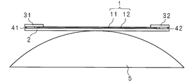
- FIGS. 2 to 4 are explanatory diagrams showing steps of bending deformation of the liquid crystal panel 1 in the first embodiment.
- FIG. 2 is a side view of the liquid crystal panel 1 and the light-transmitting plate member 2 before bending deformation.
- FIG. 2 shows a state viewed from one long side of the liquid crystal panel 1 and the translucent plate 2.
- an optical member such as BEF is placed on the central portion of the translucent plate member 2
- the liquid crystal panel 1 is disposed so as to face the TFT substrate 12 side.
- adhesive layers 41 and 42 are formed on portions outside the liquid crystal panel 1 at both short sides of the light-transmitting plate member 2. At this time, a predetermined interval may be provided between the adhesive layers 41 and 42 and the liquid crystal panel 1.
- the fixing members 31 and 32 are placed on the adhesive layers 41 and 42, respectively. At this time, the fixing members 31 and 32 are placed so that one long side follows the short side of the translucent plate 2. As the adhesive layers 41 and 42 are cured, the translucent plate 2 and the fixing members 31 and 32 are firmly joined, and both short sides of the liquid crystal panel 1 are sandwiched and integrated.
- FIG. 3 is a side view of the liquid crystal panel 1 and the translucent plate member 2 that are placed on the base and are not deformed.
- Reference numeral 5 in FIG. 3 indicates a base for bending deformation.
- the base is a half-shaped column.
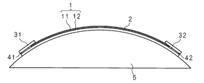
- FIG. 4 is a side view of the liquid crystal panel 1 and the light-transmitting plate member 2 after bending deformation on the base.
- the liquid crystal panel 1 is thin because the glass substrate is thin to make it easy to bend.
- the light-transmitting plate 2 having high rigidity is used as a jig to avoid applying local stress to the liquid crystal panel 1. it can.
- the translucent plate 2 has a function of diffusing light from the light source device and functions as a part of the display device, thereby reducing the number of parts and making it thinner than removing the plate that functions as an auxiliary plate later. Is possible.
- FIG. 5 is an explanatory diagram showing the force applied to the end of the liquid crystal panel 1.
- FIG. 5 shows an enlarged part of the cross section of the end portions of the liquid crystal panel 1, the translucent plate member 2, and the fixing members 31 and 32 that are integrally bent and deformed.
- the arrows in the figure indicate the physical force generated at each location.
- the thick arrow indicates the direction of the force applied to the end during bending deformation.
- the force in the direction indicated by the thick arrows applied to the end portions cannot be ignored. Due to the force applied to the end, a component force is generated in the direction toward the bending center for deformation and in the direction extending outward in the longitudinal direction of the liquid crystal panel 1.
- the liquid crystal panel 1 is curved and deformed together with the translucent plate member 2 and the fixing members 31 and 32. Therefore, the translucent plate member 2 functions as an auxiliary plate for bending deformation, and extends in the direction extending outward by the drag force. The power of is suppressed.
- the force in the extending direction is regulated by the fixing members 31 and 32, and the force for the liquid crystal panel 1 to return to the flat plate shape is also regulated by the fixing members 31 and 32. Thereby, the position shift between the CF substrate 11 and the TFT substrate 12 in the liquid crystal panel 1 is reduced.
- FIG. 6 is a schematic diagram for explaining a positional deviation between the CF substrate 11 and the TFT substrate 12.
- FIG. 6 shows an enlarged view of a cross section of the liquid crystal panel 1, and schematically shows a positional shift at the bottom.
- a liquid crystal 13 is sealed in a gap of a predetermined distance between the CF substrate 11 and the TFT substrate 12.
- a plurality of colors (R (red), G (green), B included in one pixel are formed on one TFT substrate 12 of the substrates opposed to each other with the liquid crystal 13 interposed therebetween. (Blue))
- Each pixel electrode 12T is formed corresponding to another sub-pixel.
- color filters 11R, 11G, and 11B and a black matrix 11C are formed so as to face the pixel electrodes 12T. Even in the liquid crystal panel 1 that is bent and deformed, it is difficult to maintain good display quality unless the opposing relationship between the pixel electrode 12 and the color filters 11R, 11G, and 11B is maintained with the liquid crystal 13 interposed therebetween. However, as described above, a force extending outward in the longitudinal direction of the liquid crystal panel 1 is applied to each of the CF substrate 11 and the TFT substrate 12 at the time of bending deformation. At this time, due to the difference in the radius of curvature, as shown in the lower part of FIG.
- the translucent plate 2 functions as an auxiliary plate at the time of bending deformation, and local stress is applied to the liquid crystal panel 1 when the thin liquid crystal panel 1 is bent. You can avoid that. Further, the force applied in the direction of extending the liquid crystal panel 1 applied to the end of the liquid crystal panel 1 by the drag from the auxiliary plate is suppressed. Thereby, the position shift between the CF substrate 11 and the TFT substrate 12 in the liquid crystal panel 1 is prevented. Therefore, the display quality in the liquid crystal panel 1 can be maintained.
- FIG. 7 is a perspective view showing a part of the display device in the second embodiment.
- the display device in the second embodiment includes a liquid crystal panel 1 and a translucent plate member 2.
- the display device further includes a light source device, other holding members, a housing, and the like (none of which are shown).
- the display device according to the second embodiment is the same as the configuration of the display device according to the first embodiment except for a fixed configuration between the liquid crystal panel 1 and the light-transmitting plate member 2. Therefore, the components common to the display device in Embodiment 1 are denoted by the same reference numerals, and detailed description thereof is omitted.
- the translucent plate 2 is bonded to the back side of the liquid crystal panel 1 with an adhesive layer 6.
- the adhesive layer 6 is formed of a rubber adhesive that is transparent after curing and has elasticity.
- the adhesive layer 6 adheres a range along the outer edge portion of the TFT substrate 12 of the liquid crystal panel 1.
- the thickness of the adhesive layer 6 is preferably 1 mm or more, for example.
- the light source device is disposed opposite to the light transmitting plate member 2 side of the liquid crystal panel 1 and the light transmitting plate member 2 that are curved as described above, and further the liquid crystal panel, the light transmitting plate member 2 and the light source device. It is comprised with the holding member and housing
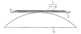
- FIG. 8 to FIG. 10 are explanatory diagrams showing the process of bending deformation of the liquid crystal panel 1 in the second embodiment.
- FIG. 8 is a side view of the liquid crystal panel 1 and the light-transmitting plate member 2 before bending deformation.
- FIG. 8 shows a state viewed from one long side of the liquid crystal panel 1 and the translucent plate member 2.
- the adhesive layer 6 it arrange
- the adhesive layer 6 may be formed in advance on the TFT substrate 12 side.
- FIG. 9 is a side view of the liquid crystal panel 1 and the translucent plate 2 that are placed on the base 5 and are not deformed by bending.
- FIG. 10 is a side view of the liquid crystal panel 1 and the light-transmitting plate member 2 after bending deformation on the base 5.
- the liquid crystal panel 1 is bent and deformed integrally with the translucent plate 2, and therefore, the translucent plate 2 having high rigidity is used as a jig, and local stress is applied to the liquid crystal panel 1. Can be avoided. Further, the translucent plate 2 functions as an auxiliary plate at the time of bending deformation, and the force to extend the liquid crystal panel 1 applied to the end of the liquid crystal panel 1 by the drag from the auxiliary plate is suppressed. Thereby, the position shift between the CF substrate 11 and the TFT substrate 12 in the liquid crystal panel 1 is prevented. Therefore, the display quality in the liquid crystal panel 1 can be maintained.
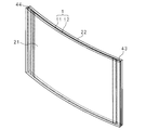
- FIG. 11 is a perspective view illustrating part of the display device according to Embodiment 3.
- the display device in the third embodiment includes a liquid crystal panel 1 and translucent plates 21 and 22.
- the display device further includes a light source device, other holding members, a housing, and the like (none of which are shown). Since the liquid crystal panel 1 of the display device in the third embodiment has the same configuration as the liquid crystal panel 1 in the first embodiment, the same reference numerals are given and detailed description thereof is omitted.
- the translucent plates 21 and 22 are obtained by curving the longitudinal direction of a transparent rectangular flat plate.
- the translucent plates 21 and 22 are larger than the liquid crystal panel 1 and have substantially the same size.
- the translucent plate 21 is made of a polymer material having high transparency such as PMMA (Poly (methyl methacrylate)).
- the other light transmissive member 22 may also be configured as a diffusion plate by dispersing particles having different refractive indexes in the above-described polymer material in order to share a part of the function of the optical sheet as will be described later. .
- the thickness of the translucent plates 21 and 22 is larger than that of the liquid crystal panel 1.
- the translucent plate material 2 preferably has higher rigidity than the liquid crystal panel 1.
- the liquid crystal panel 1 has a thickness of about 1 mm
- the translucent plates 21 and 22 have a thickness of about 0.5 to 2 mm.
- the thickness may be the same as long as it can withstand the radius of curvature desired to be curved and is sufficiently high in rigidity to suppress the swell when the liquid crystal panel 1 is curved.
- the translucent plates 21 and 22 are arranged with the liquid crystal panel 1 sandwiched therebetween, and portions outside the liquid crystal panel 1 are bonded by adhesive layers 43 and 44, respectively. At this time, the display surface side of the liquid crystal panel 1 is arranged on the one light-transmitting plate 21 side. The liquid crystal panel 1 is sandwiched between translucent plates 21 and 22. At this time, it is preferable that BEF is sandwiched between the TFT substrate 12 side of the liquid crystal panel 1 and the translucent plate material 22.
- the light source device is disposed opposite to the liquid crystal panel 1 and the light transmitting plate members 21 and 22 that are curved as described above, and the liquid crystal panel 1 and the light transmitting plate member 21 are disposed.
- , 22 and the light source device are both comprised of a holding member and a housing.
- the holding member may be positioned and held so as to maintain a predetermined distance between the liquid crystal panel 1 and the light source device, and the housing may cover the outer periphery other than the display area of the liquid crystal panel 1.
- FIG. 12 to FIG. 14 are explanatory views showing the process of bending deformation of the liquid crystal panel 1 in the third embodiment.
- FIG. 12 is a side view of the liquid crystal panel 1 and the translucent plates 21 and 22 before bending deformation in the third embodiment.
- FIG. 12 shows a state viewed from one long side of the liquid crystal panel 1 and the translucent plates 21 and 22.
- an optical member such as BEF is placed on the central portion of the light-transmitting plate material 22 among the light-transmitting plate materials 21 and 22, and then disposed so that the TFT substrate 12 side of the liquid crystal panel 1 faces.
- adhesive layers 43 and 44 are formed on the portion of the translucent plate material 22 outside the liquid crystal panel 1. At this time, a predetermined interval is provided between the adhesive layers 43 and 44 and both short sides of the liquid crystal panel 1.
- the translucent plate 21 is placed on the adhesive layers 43 and 44 so that both short sides are placed so that the liquid crystal panel 1 is sandwiched between the translucent plate 22. Then, the liquid crystal panel 1 is sandwiched between the translucent plates 21 and 22 by the curing of the adhesive layers 43 and 44.
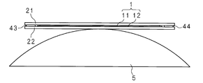
- FIG. 12 is a side view of the liquid crystal panel 1 and the translucent plates 21 and 22 before being deformed and placed on the base 5.
- FIG. 13 is a side view of the liquid crystal panel 1 and the translucent plates 21 and 22 after bending deformation on the base 5.
- the liquid crystal panel 1 is integrally curved and deformed together with the translucent plates 21 and 22, so that the translucent plates 21 and 22 function as auxiliary plates at the time of the curved deformation, and the liquid crystal panel 1 is configured to be thin. It is possible to avoid applying local stress to the liquid crystal panel 1 when bending the liquid crystal panel 1. Moreover, the force which extends the liquid crystal panel 1 added to the edge part of the liquid crystal panel 1 in the longitudinal direction by the drag from the auxiliary plate is suppressed. In the third embodiment, the lift from the light transmitting plate 22 on both short sides can be regulated by the force with which the liquid crystal panel 1 returns to a flat plate shape by the light transmitting plate 21. Thereby, the positional deviation between the CF substrate 11 and the TFT substrate 12 in the liquid crystal panel 1 is reduced. Therefore, the display quality in the liquid crystal panel 1 can be maintained.
- the liquid crystal panel 1 is configured to bend in the longitudinal direction so that the display surface side is convex.
- the present invention is not limited thereto, and the display surface side may be curved so as to be concave, or the liquid crystal panel 1 may be curved in the lateral direction.
Landscapes
- Physics & Mathematics (AREA)
- Nonlinear Science (AREA)
- Mathematical Physics (AREA)
- Chemical & Material Sciences (AREA)
- Crystallography & Structural Chemistry (AREA)
- General Physics & Mathematics (AREA)
- Optics & Photonics (AREA)
- Liquid Crystal (AREA)
- Devices For Indicating Variable Information By Combining Individual Elements (AREA)
Abstract
Description
図1は、実施の形態1における表示装置の要部を示す斜視図である。表示装置は、液晶パネル1、透光板材2及び固定部材31,32を含む。表示装置は液晶パネル1の他、更に光源装置、その他保持部材、筐体等(いずれも図示せず)を含んで構成される。
実施の形態1の表示装置を作製するに際してはまず、液晶パネル1を透光板材2と一体化させる。
図2は、湾曲変形前の液晶パネル1及び透光板材2の側面図である。図2は、液晶パネル1及び透光板材2の一長辺側から見た状態を示している。透光板材2の中央部分上に、BEF等の光学部材が載置された後、液晶パネル1のTFT基板12側が対向するように配置される。次に、透光板材2の両短辺部における液晶パネル1外の部分に、接着層41,42が形成される。このとき接着層41,42と液晶パネル1との間には所定の間隔が設けられているとよい。そして接着層41,42上に固定部材31,32が夫々載置される。このとき固定部材31,32は、透光板材2の短辺に一長辺が沿うように載置される。接着層41,42の硬化により、透光板材2及び固定部材31,32が強固に接合され、液晶パネル1の両短辺部が挟持されて一体化する。
次に(1)に示した一体化した液晶パネル1、透光板材2及び固定部材31,32を共に一体的に湾曲変形させる。図3は、土台上に載置された湾曲変形前の液晶パネル1及び透光板材2の側面図である。図3中の符号5は湾曲変形用の土台を示す。土台は半割型の円柱状をなしている。図4は、土台上の湾曲変形後の液晶パネル1及び透光板材2の側面図である。
図7は、実施の形態2における表示装置の一部を示す斜視図である。実施の形態2における表示装置は、液晶パネル1、透光板材2を含む。表示装置は液晶パネル1の他、更に光源装置、その他保持部材、筐体等(いずれも図示せず)を含んで構成される。実施の形態2における表示装置は、液晶パネル1及び透光板材2間の固定の構成以外は実施の形態1における表示装置の構成と同様である。したがって、実施の形態1における表示装置と共通する構成については同一の符号を付して詳細な説明を省略する。
実施の形態2においても、表示装置を作製するに際してはまず、液晶パネル1を透光板材2と一体化させる。
図8は、湾曲変形前の液晶パネル1及び透光板材2の側面図である。図8は、液晶パネル1及び透光板材2の一長辺側から見た状態を示している。透光板材2の中央部分上に、BEF等の光学部材が載置された後、該光学部材を囲うように、更に対向配置されるTFT基板12に対応する範囲の外周に沿うようにして帯状の接着層6が形成される。接着層6は面接着としないことが好ましい。湾曲変形時にTFT基板12に接着層6からの張力が加わり、ガラス割れの原因となり得るからである。次に接着層6上に、液晶パネル1のTFT基板12側が対向するように配置される。接着層6の硬化により、液晶パネル1と透光板材2とが一体化する。接着層6は予めTFT基板12側に形成されていてもよい。
次に(1)に示した液晶パネル1及び透光板材2が共に一体的に湾曲変形される。図9は、土台5上に載置された湾曲変形前の液晶パネル1及び透光板材2の側面図である。図10は、土台5上の湾曲変形後の液晶パネル1及び透光板材2の側面図である。
図11は、実施の形態3における表示装置の一部を示す斜視図である。実施の形態3における表示装置は、液晶パネル1、透光板材21,22を含む。表示装置は液晶パネル1の他、更に光源装置、その他保持部材、筐体等(いずれも図示せず)を含んで構成される。実施の形態3における表示装置の液晶パネル1は実施の形態1における液晶パネル1と同一の構成であるから同一の符号を付して詳細な説明を省略する。
図12は、実施の形態3における湾曲変形前の液晶パネル1及び透光板材21,22の側面図である。図12は、液晶パネル1及び透光板材21,22の一長辺側から見た状態を示している。まず透光板材21,22の内、透光板材22の中央部上に、BEF等の光学部材が載置された後、液晶パネル1のTFT基板12側が対向するように配置される。次に、透光板材22の液晶パネル1外の部分に接着層43,44が形成される。このとき接着層43,44と液晶パネル1の両短辺との間には所定の間隔が設けられている。透光板材22との間で液晶パネル1を挟むようにして、透光板材21が接着層43,44上に両短辺部を載せるようにして載置される。そして接着層43,44の硬化により、液晶パネル1は透光板材21,22に挟持される。
次に(1)に示した液晶パネル1及び透光板材21,22が共に一体的に湾曲変形される。図12は、土台5上に載置された湾曲変形前の液晶パネル1及び透光板材21,22の側面図である。図13は、土台5上の湾曲変形後の液晶パネル1及び透光板材21,22の側面図である。
11 CF基板
12 TFT基板
13 液晶
2,21,22 透光板材(板材)
31,32 固定部材(板材)
41,42,43,44 接着層
6 接着層
Claims (6)
- 一対のガラス基板を対向させて該ガラス基板間に液晶を封入してあり、湾曲させてある液晶パネルを備える表示装置において、
前記液晶パネルの湾曲の内側である一面側に配置されており、前記液晶パネルよりも大きく、前記液晶パネルに沿って湾曲されている透光性の板材
を備えることを特徴とする表示装置。 - 前記板材の前記液晶パネル側の面における相対する2つの縁辺部に夫々、前記板材との間で前記液晶パネルを挟みこむように縁辺に沿って配置されている他の板材と、
前記板材及び他の板材間の前記液晶パネルに対応する範囲外の部分を接着する接着層と
を更に備えることを特徴とする請求項1に記載の表示装置。 - 前記板材は前記液晶パネルの前記一面側に接着されている
ことを特徴とする請求項1に記載の表示装置。 - 前記液晶パネルの他面側に配置されており、前記板材と略同じ大きさであって前記液晶パネルに沿って湾曲されている他の板材と、
前記板材及び他の板材の前記液晶パネルに対応する範囲外の部分を接着する接着層と
を更に備えることを特徴とする請求項1に記載の表示装置。 - 前記板材は前記液晶パネルよりも剛性が高い
ことを特徴とする請求項1から4のいずれか1つに記載の表示装置。 - 一対のガラス基板を対向させて該ガラス基板間に液晶を封入してある液晶パネルを湾曲させた表示装置を製造する製造方法において、
前記液晶パネルを湾曲する前に、透光性を有しており前記液晶パネルよりも大きい板材上に前記液晶パネルを載置し、
前記板材及び前記液晶パネル間を係止させ、
前記板材及び液晶パネルを一体的に、前記板材を内側にして湾曲変形させる
ことを特徴とする表示装置の製造方法。
Priority Applications (4)
| Application Number | Priority Date | Filing Date | Title |
|---|---|---|---|
| JP2017551476A JPWO2017085846A1 (ja) | 2015-11-19 | 2015-11-19 | 表示装置及び表示装置の製造方法 |
| CN201580084686.XA CN108496109A (zh) | 2015-11-19 | 2015-11-19 | 显示装置和显示装置的制造方法 |
| US15/777,143 US20180329239A1 (en) | 2015-11-19 | 2015-11-19 | Display device and method for producing display device |
| PCT/JP2015/082613 WO2017085846A1 (ja) | 2015-11-19 | 2015-11-19 | 表示装置及び表示装置の製造方法 |
Applications Claiming Priority (1)
| Application Number | Priority Date | Filing Date | Title |
|---|---|---|---|
| PCT/JP2015/082613 WO2017085846A1 (ja) | 2015-11-19 | 2015-11-19 | 表示装置及び表示装置の製造方法 |
Publications (1)
| Publication Number | Publication Date |
|---|---|
| WO2017085846A1 true WO2017085846A1 (ja) | 2017-05-26 |
Family
ID=58718495
Family Applications (1)
| Application Number | Title | Priority Date | Filing Date |
|---|---|---|---|
| PCT/JP2015/082613 Ceased WO2017085846A1 (ja) | 2015-11-19 | 2015-11-19 | 表示装置及び表示装置の製造方法 |
Country Status (4)
| Country | Link |
|---|---|
| US (1) | US20180329239A1 (ja) |
| JP (1) | JPWO2017085846A1 (ja) |
| CN (1) | CN108496109A (ja) |
| WO (1) | WO2017085846A1 (ja) |
Families Citing this family (2)
| Publication number | Priority date | Publication date | Assignee | Title |
|---|---|---|---|---|
| CN113299188B (zh) * | 2021-05-08 | 2022-04-26 | 武汉华星光电技术有限公司 | 显示面板及其制作方法 |
| TWI793056B (zh) * | 2022-10-03 | 2023-02-11 | 達擎股份有限公司 | 顯示裝置 |
Citations (3)
| Publication number | Priority date | Publication date | Assignee | Title |
|---|---|---|---|---|
| JPH0481120U (ja) * | 1990-11-27 | 1992-07-15 | ||
| US20090284904A1 (en) * | 2008-05-16 | 2009-11-19 | Jer-Yao Wu | Curved Display Panel and Method for Manufacturing the same |
| JP2015007699A (ja) * | 2013-06-25 | 2015-01-15 | 三菱電機株式会社 | 液晶表示装置及びその製造方法 |
Family Cites Families (9)
| Publication number | Priority date | Publication date | Assignee | Title |
|---|---|---|---|---|
| TWI277042B (en) * | 2003-10-28 | 2007-03-21 | Seiko Epson Corp | Electro-optical device, electronic equipment, and method of manufacturing electro-optical device |
| JP3938134B2 (ja) * | 2003-10-28 | 2007-06-27 | セイコーエプソン株式会社 | 電気光学装置、およびそれを用いた電子機器 |
| JP2008089847A (ja) * | 2006-09-29 | 2008-04-17 | Optrex Corp | 表示装置 |
| JP5174781B2 (ja) * | 2009-10-15 | 2013-04-03 | 三菱電機株式会社 | 表示装置およびその製造方法 |
| TWI457880B (zh) * | 2010-09-30 | 2014-10-21 | E Ink Holdings Inc | 曲面顯示模組與顯示裝置 |
| KR101333770B1 (ko) * | 2011-11-24 | 2013-11-29 | 주식회사 토비스 | 에칭 장치와, 이를 포함한 곡면 디스플레이 패널 제조 장치와, 이를 이용한 곡면 디스플레이 패널 제조 방법과, 그리고 이에 의해 제조된 곡면 디스플레이 패널 |
| US9470919B2 (en) * | 2013-05-14 | 2016-10-18 | Microsoft Technology Licensing, Llc | Methods for producing a glass-based non planar digital display |
| KR101746650B1 (ko) * | 2014-09-02 | 2017-06-14 | 주식회사 토비스 | 곡면형 디스플레이 제조장치 및 곡면형 디스플레이 제조방법 |
| US9917266B2 (en) * | 2015-08-17 | 2018-03-13 | Microsoft Technology Licensing, Llc | Bendable device with a window top layer and a body having extendable bending region |
-
2015
- 2015-11-19 JP JP2017551476A patent/JPWO2017085846A1/ja active Pending
- 2015-11-19 WO PCT/JP2015/082613 patent/WO2017085846A1/ja not_active Ceased
- 2015-11-19 US US15/777,143 patent/US20180329239A1/en not_active Abandoned
- 2015-11-19 CN CN201580084686.XA patent/CN108496109A/zh not_active Withdrawn
Patent Citations (3)
| Publication number | Priority date | Publication date | Assignee | Title |
|---|---|---|---|---|
| JPH0481120U (ja) * | 1990-11-27 | 1992-07-15 | ||
| US20090284904A1 (en) * | 2008-05-16 | 2009-11-19 | Jer-Yao Wu | Curved Display Panel and Method for Manufacturing the same |
| JP2015007699A (ja) * | 2013-06-25 | 2015-01-15 | 三菱電機株式会社 | 液晶表示装置及びその製造方法 |
Also Published As
| Publication number | Publication date |
|---|---|
| JPWO2017085846A1 (ja) | 2018-09-06 |
| US20180329239A1 (en) | 2018-11-15 |
| CN108496109A (zh) | 2018-09-04 |
Similar Documents
| Publication | Publication Date | Title |
|---|---|---|
| US9523875B2 (en) | Method for manufacturing curved-surface display | |
| JP6122439B2 (ja) | 曲面ディスプレイパネル製造方法 | |
| AU2012305101B2 (en) | Method for manufacturing curved-surface display | |
| KR101007461B1 (ko) | 액정 표시 장치 | |
| US8982545B2 (en) | Curved-surface display panel fabrication method, curved-surface display panel using same, and multi-image display device using same | |
| JP5684391B2 (ja) | 曲面ディスプレイパネル製造方法および曲面ディスプレイパネル | |
| CN101641634B (zh) | 带微透镜阵列的液晶显示面板及其制造方法 | |
| JP2013504789A (ja) | 曲面状のディスプレイパネル製造方法 | |
| CN101520562B (zh) | 液晶显示装置 | |
| JP2007272107A (ja) | 表示装置 | |
| JP2010156784A (ja) | 液晶表示装置 | |
| JP2012198434A (ja) | 液晶表示装置 | |
| WO2016088615A1 (ja) | 湾曲型表示パネルの製造方法 | |
| CN102362304A (zh) | 显示装置和其制造方法 | |
| CN104216155A (zh) | 显示单元 | |
| JP2006106079A (ja) | 電気光学装置、それを用いた電子機器、および電気光学装置の製造方法 | |
| JP4335632B2 (ja) | 液晶表示装置の製造方法 | |
| JP2006098525A (ja) | 光学部品及びその製造方法並びに当該方法で製造された光学部品を有する液晶表示装置 | |
| JP2010066706A (ja) | 液晶表示装置 | |
| JPWO2017085846A1 (ja) | 表示装置及び表示装置の製造方法 | |
| US10295729B2 (en) | Liquid crystal display device | |
| CN101995701A (zh) | 液晶显示器及其制造方法 | |
| JP2010060840A (ja) | 表示装置 | |
| JP2012073356A (ja) | 液晶表示装置 | |
| JP2005300829A (ja) | ペン入力型液晶表示装置 |
Legal Events
| Date | Code | Title | Description |
|---|---|---|---|
| 121 | Ep: the epo has been informed by wipo that ep was designated in this application |
Ref document number: 15908786 Country of ref document: EP Kind code of ref document: A1 |
|
| WWE | Wipo information: entry into national phase |
Ref document number: 15777143 Country of ref document: US |
|
| ENP | Entry into the national phase |
Ref document number: 2017551476 Country of ref document: JP Kind code of ref document: A |
|
| NENP | Non-entry into the national phase |
Ref country code: DE |
|
| 122 | Ep: pct application non-entry in european phase |
Ref document number: 15908786 Country of ref document: EP Kind code of ref document: A1 |