WO2017082379A1 - 磁気検出装置 - Google Patents
磁気検出装置 Download PDFInfo
- Publication number
- WO2017082379A1 WO2017082379A1 PCT/JP2016/083481 JP2016083481W WO2017082379A1 WO 2017082379 A1 WO2017082379 A1 WO 2017082379A1 JP 2016083481 W JP2016083481 W JP 2016083481W WO 2017082379 A1 WO2017082379 A1 WO 2017082379A1
- Authority
- WO
- WIPO (PCT)
- Prior art keywords
- magnetic
- calibration
- magnetic field
- sensor
- detection device
- Prior art date
- Legal status (The legal status is an assumption and is not a legal conclusion. Google has not performed a legal analysis and makes no representation as to the accuracy of the status listed.)
- Ceased
Links
Images





Classifications
-
- G—PHYSICS
- G01—MEASURING; TESTING
- G01R—MEASURING ELECTRIC VARIABLES; MEASURING MAGNETIC VARIABLES
- G01R35/00—Testing or calibrating of apparatus covered by the other groups of this subclass
- G01R35/005—Calibrating; Standards or reference devices, e.g. voltage or resistance standards, "golden" references
-
- G—PHYSICS
- G01—MEASURING; TESTING
- G01R—MEASURING ELECTRIC VARIABLES; MEASURING MAGNETIC VARIABLES
- G01R33/00—Arrangements or instruments for measuring magnetic variables
- G01R33/02—Measuring direction or magnitude of magnetic fields or magnetic flux
- G01R33/06—Measuring direction or magnitude of magnetic fields or magnetic flux using galvano-magnetic devices
- G01R33/09—Magnetoresistive devices
-
- G—PHYSICS
- G01—MEASURING; TESTING
- G01V—GEOPHYSICS; GRAVITATIONAL MEASUREMENTS; DETECTING MASSES OR OBJECTS; TAGS
- G01V3/00—Electric or magnetic prospecting or detecting; Measuring magnetic field characteristics of the earth, e.g. declination, deviation
- G01V3/08—Electric or magnetic prospecting or detecting; Measuring magnetic field characteristics of the earth, e.g. declination, deviation operating with magnetic or electric fields produced or modified by objects or geological structures or by detecting devices
-
- G—PHYSICS
- G01—MEASURING; TESTING
- G01V—GEOPHYSICS; GRAVITATIONAL MEASUREMENTS; DETECTING MASSES OR OBJECTS; TAGS
- G01V3/00—Electric or magnetic prospecting or detecting; Measuring magnetic field characteristics of the earth, e.g. declination, deviation
- G01V3/08—Electric or magnetic prospecting or detecting; Measuring magnetic field characteristics of the earth, e.g. declination, deviation operating with magnetic or electric fields produced or modified by objects or geological structures or by detecting devices
- G01V3/081—Electric or magnetic prospecting or detecting; Measuring magnetic field characteristics of the earth, e.g. declination, deviation operating with magnetic or electric fields produced or modified by objects or geological structures or by detecting devices the magnetic field is produced by the objects or geological structures
-
- G—PHYSICS
- G07—CHECKING-DEVICES
- G07D—HANDLING OF COINS OR VALUABLE PAPERS, e.g. TESTING, SORTING BY DENOMINATIONS, COUNTING, DISPENSING, CHANGING OR DEPOSITING
- G07D7/00—Testing specially adapted to determine the identity or genuineness of valuable papers or for segregating those which are unacceptable, e.g. banknotes that are alien to a currency
- G07D7/04—Testing magnetic properties of the materials thereof, e.g. by detection of magnetic imprint
-
- G—PHYSICS
- G07—CHECKING-DEVICES
- G07D—HANDLING OF COINS OR VALUABLE PAPERS, e.g. TESTING, SORTING BY DENOMINATIONS, COUNTING, DISPENSING, CHANGING OR DEPOSITING
- G07D7/00—Testing specially adapted to determine the identity or genuineness of valuable papers or for segregating those which are unacceptable, e.g. banknotes that are alien to a currency
- G07D7/20—Testing patterns thereon
- G07D7/2075—Setting acceptance levels or parameters
Definitions
- the present invention relates to a magnetic detection device for detecting the magnetism of a paper sheet.
- a magnetic detection device for detecting the magnetism of a conveyed paper sheet.
- a magnetic detection device is built in the apparatus, the magnetic characteristics of the banknotes are detected by the magnetic detection apparatus, and the authenticity of the banknotes is identified using the detection results.
- the magnetic detection device for example, a plurality of magnetic sensors are arranged in a straight line, and the magnetic detection of the bill is performed after the plurality of magnetic sensors are calibrated.
- Patent Document 1 a linear conductor is arranged according to a plurality of sensors arranged in a line, and a current is passed through the conductor to generate a magnetic field for calibration to calibrate each magnetic sensor.
- Patent Document 2 also discloses an apparatus for calibrating a magnetic sensor by generating a calibration magnetic field with a rectangular plate-shaped conductor.
- the present invention has been made to solve the above-described problems caused by the prior art, and an object of the present invention is to provide a small-sized magnetic detection device capable of calibrating a plurality of magnetic sensors with high accuracy.
- the present invention provides a magnetic detection device for detecting the magnetism of a conveyed paper sheet, and linearly extends in a direction perpendicular to the transport direction of the paper sheet.
- a plurality of magnetic sensors arranged, a plate-like excitation member that is long in the arrangement direction of the magnetic sensors, a current in the arrangement direction is caused to flow through the excitation member to generate a magnetic field for calibration, and the magnetic sensor
- a control unit for obtaining a correction value for correcting the sensitivity variation of the magnetic sensor based on the detection result of the magnetic field for calibration.
- the present invention is characterized in that, in the above invention, the excitation member is a cover that exposes at least a part of one surface as a magnetic detection surface to the outside of the apparatus.
- the present invention is characterized in that, in the above-mentioned invention, the exciting member is grounded and a current is applied only while the calibration magnetic field is generated.
- a calibration magnetic field is generated on the lower surface side of the excitation member such that the direction of the magnetic field is substantially parallel to the lower surface of the excitation member and substantially perpendicular to the arrangement direction of the magnetic sensors. It is characterized by that.
- a calibration magnetic field is generated on the side surface side of the excitation member so that the direction of the magnetic field is substantially parallel to the side surface of the excitation member and substantially perpendicular to the arrangement direction of the magnetic sensor. It is characterized by that.
- the control unit generates and stores an initial correction value for correcting a sensitivity variation of each magnetic sensor by generating a magnetic field for calibration by the exciting member at the time of manufacture, and stores the paper sheet.
- a magnetic field for calibration is generated by the excitation member, and the detected value of the magnetic field for calibration by the magnetic sensor is corrected with the initial correction value, and each magnetic field is determined based on the corrected value.
- a correction value at the time of measurement for correcting the sensitivity variation of the sensor is obtained, and at the time of magnetic detection of the paper sheet, the magnetic detection value of the paper sheet is corrected by the correction value at the time of measurement.
- the calibration member when the correction value is obtained, the calibration member generates a calibration magnetic field again after performing a predetermined number of operations of generating the calibration magnetic field by the excitation member.
- requires is performed.
- the present invention is characterized in that, in the above-mentioned invention, the magnetic sensor includes two magnetosensitive elements.
- the present invention is the above invention, wherein the magnetic sensor is supported in an inclined state in the apparatus so that a distance from a conveyance surface for conveying the paper sheet is different between the two magnetosensitive elements.
- a magnetic field for calibration is generated by an excitation member of a rectangular plate-like body that is long in the arrangement direction of the magnetic sensors, thereby correcting sensitivity variations of the magnetic sensors.
- a correction value can be obtained.
- the excitation member as a cover that covers the magnetic sensor, it is possible to reduce the size of the magnetic detection device as compared with the case where the excitation member is provided between the cover and the magnetic sensor. This makes it possible to arrange the magnetic sensor closer to the paper sheet, which is advantageous for increasing the resolution of the magnetic sensor.
- FIG. 1 is a schematic diagram showing an appearance of the magnetic detection device according to the present embodiment.
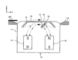
- FIG. 2 is a schematic cross-sectional view showing the internal structure of the magnetic detection device viewed from the side.
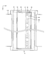
- FIG. 3 is a schematic diagram showing the magnetic detection device viewed from above.
- FIG. 4 is a diagram showing a calibration circuit for generating a calibration magnetic field by the sensor cover.
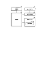
- FIG. 5 is a block diagram showing an outline of a functional configuration of the magnetic detection device.
- FIG. 6 is a diagram for explaining the calibration process at the time of manufacture.
- FIG. 7 is a diagram for explaining the calibration process at the time of measurement.
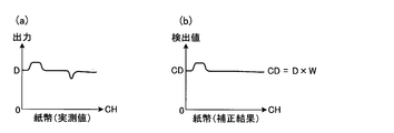
- FIG. 8 is a diagram for explaining the magnetism detection processing of banknotes.
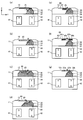
- FIG. 9 is a diagram illustrating an example of a cross-sectional shape of the excitation member and a calibration magnetic field generated around the excitation member.
- FIG. 10 is a diagram illustrating different examples of excitation members that generate a calibration magnetic field.
- the magnetic detection device has a function of detecting the magnetism of the paper sheet.
- a magnetic detection apparatus is provided in a banknote processing apparatus, and is utilized in order to detect the magnetic characteristic of the banknote conveyed in the apparatus and identify the authenticity etc. of this banknote is demonstrated to an example.
- FIG. 1 is a schematic diagram showing an appearance of a magnetic detection device 10 according to the present embodiment.
- the magnetic detection device 10 is disposed in a transport path 110 through which the bill 100 is transported in the bill processing apparatus.
- the magnetic detection device 10 is arranged such that the upper surface of the device including the sensor cover (excitation member) 20 forms the same plane as the conveyance surface of the conveyance path 110.
- conveyance of the banknote 100 is regulated so that it is conveyed between the two broken lines shown in FIG. 1, and the banknote 100 is conveyed in the positive direction of the Y axis using a plurality of rollers, belts, and the like. Is done.
- FIG. 1 is a schematic diagram showing an appearance of a magnetic detection device 10 according to the present embodiment.
- the magnetic detection device 10 is disposed in a transport path 110 through which the bill 100 is transported in the bill processing apparatus.
- the magnetic detection device 10 is arranged such that the upper surface of the device including the sensor cover (excitation member) 20 forms the same plane as
- FIG. 1 shows an example in which the magnetic detection device 10 is disposed below the conveyance path 110, the magnetic detection device 10 may be disposed above the conveyance path 110.
- FIG. 2 is a schematic cross-sectional view showing the internal structure of the magnetic detection device 10 as viewed from the side.
- FIG. 3 is a schematic diagram showing the magnetic detection device 10 as viewed from above.
- two bias magnets 41 and 42 for generating a bias magnetic field in a resin case 11 made of a nonmagnetic material, and a change in magnetic field when the banknote 100 passes through the bias magnetic field.
- a magnetic sensor 30 for detecting.
- the magnetic sensor 30 has two magnetosensitive elements 31 and 32 and is supported in an inclined state in the case 11.
- the distance in the Z-axis direction from the conveyance surface of the conveyance path 110 to the one magnetosensitive element 31 is in a state where the distance from the conveyance surface to the other magnetosensitive element 32 is greater than the distance in the Z-axis direction. Tilted like that.
- a bias magnetic field (broken line in the figure) generated around the bias magnets 41 and 42 and a calibration generated around the sensor cover 20 are shown.
- the magnetic field for use (one-dot chain line in the figure) is shown separately.
- a single-channel magnetic sensor 30 is formed by the two magnetosensitive elements 31 and 32, and as shown in FIG. 3, a plurality of channels (for example, 200 channels) of magnetic sensors 30 (30a, 30b...) Are formed on a single substrate. It is supported by the sensor support portion 33 in a state of being linearly arranged on the top.
- the magnetic sensors 30 are arranged in a line in a direction (X-axis direction) perpendicular to the conveyance direction (Y-axis direction) of the banknote 100, and the entire width direction in the X-axis direction of the banknote 100 being conveyed on the conveyance path 110. Magnetism can be detected.
- the magnetic sensor 30 can detect magnetism on the entire surface of the banknote 100.
- Magnetic field is generated.
- the magnetic sensor 30 is arranged so as to detect the amount of change in the bias magnetic field caused by the magnetic material passing through the transport path 110.
- the magnetic sensor 30 includes, for example, two magnetosensitive elements 31 and 32 each including a magnetoresistive element, and outputs a change in resistance value of the two magnetoresistive elements as a change in voltage value.
- the magnetic detection device 10 can detect the magnetic amount of the magnetic substance contained in the banknote 100 by using this voltage value as a detection signal for the magnetic substance.
- the magnetic sensor 30 is arranged in an inclined state so as to form an angle with the conveyance surface (XY plane) on which the banknote 100 is conveyed, and has a function of outputting a detection signal corresponding to the amount of magnetism of the magnetic material.
- XY plane conveyance surface
- a magnetic sensor 30 is described in International Publication No. WO2014 / 168180, its details are omitted.
- a sensor cover 20 made of a conductive nonmagnetic material is provided on the upper surface side of the case 11 so as to cover the magnetic sensor 30.
- the sensor cover 20 has a shape in which both outer sides of a rectangular thin plate that is long in the X-axis direction are bent downward, a flat portion parallel to the XY plane, and two slopes on both outer sides of the flat portion. Part.
- the magnetic sensor 30 is disposed below the plane portion between the inclined portions on both outer sides of the sensor cover 20.
- the sensor cover 20 is supported in a state where a part of the upper surface is exposed from the opening 12 of the case 11.
- the upper surface of the sensor cover 20 exposed from the opening 12 forms the same plane as the transport surface of the transport path 110 that transports the banknote 100.
- the magnetic sensor 30 detects the magnetism of the bill 100 passing through the upper surface of the sensor cover 20.
- the banknote 100 passes through the upper surface side of the flat surface portion so as to be pressed against the sensor cover 20 by a brush roller (not shown) provided above the flat surface portion of the sensor cover 20.
- the sensor cover 20 is formed of a material having wear resistance.
- the sensor cover 20 is formed using a nonmagnetic conductor such as stainless steel, brass, or titanium, or conductive ceramics.
- the magnetic detection device 10 is characterized in that the sensor cover 20 is used as an excitation member that generates a magnetic field for calibration for calibrating the magnetic sensor 30.
- a calibration magnetic field is generated around the sensor cover 20 as shown by a one-dot chain line in FIG. .
- the direction of the magnetic field for calibration is the Y-axis direction.
- the magnetic field direction and the magnetic field strength of the calibration magnetic field are substantially the same, and therefore, in a straight line parallel to the X axis.
- FIG. 4 is a diagram showing a calibration circuit 50 for generating a calibration magnetic field by the sensor cover 20.
- the voltage on / off switch 51 is a switching circuit using a transistor such as a MOSFET, and has a function of flowing a pulsed current through the sensor cover 20 by performing on / off control of voltage application.
- the constant current control circuit 52 is a circuit using an operational amplifier or the like, and has a function of controlling the current value flowing through the sensor cover 20 to be constant when a voltage is applied by a voltage on / off switch.
- a diode for preventing static electricity is provided between the constant current control circuit 52 and the ground.
- the sensor cover 20 is connected to the ground to generate a calibration magnetic field.
- the influence of external noise such as static electricity or electric field noise on the magnetic sensor 30 is prevented.
- FIG. 5 is a block diagram showing an outline of the functional configuration of the magnetic detection device 10.
- the magnetic detection device 10 includes a control unit 60 and a storage unit 70 in addition to the configuration described above.
- the control unit 60 controls the calibration circuit 50 to generate a calibration magnetic field around the sensor cover 20, and controls the magnetic detection operation by the magnetic sensor 30 to control the magnetism by the magnetic sensor 30.
- the correction value for correcting the sensitivity variation of each magnetic sensor 30 is determined.
- the storage unit 70 is a nonvolatile storage device.
- the control unit 60 stores data related to the correction value of the magnetic sensor 30 in the storage unit 70.
- the control unit 60 of the magnetic detection device 10 is connected to the control unit of the banknote processing device including the magnetic detection device 10, and transmits and receives data to and from the control unit of the banknote processing device. It has a function.
- the banknote handling apparatus has a function of detecting a position on the transport path 110 of the banknote 100 transported toward the magnetic detection device 10 using a transport path sensor or the like including a light projecting / receiving unit provided in the transport path 110. is doing.
- the control unit 60 of the magnetic detection device 10 acquires information related to the transport position of the banknote 100 on the transport path 110 from the banknote processing apparatus, and the banknote 100 detects the magnetic detection region by the magnetic sensor 30. The process which detects the magnetism of the banknote 100 is performed according to passing.
- the magnetic detection apparatus 10 is not limited to the aspect which has the control part 60 and the memory
- storage part of the banknote processing apparatus which incorporates the magnetic detection apparatus 10 are the control parts 60 shown in FIG. Also, it may be an aspect that operates as the storage unit 70.
- the magnetic detection device 10 corrects the sensitivity variation by performing two types of calibration processing, that is, calibration processing at the time of manufacture and calibration processing at the time of measurement.
- the calibration process at the time of manufacture is performed in the state where there is no influence by external noise or the like when the magnetic detection device 10 is manufactured. This is a calibration process for obtaining an initial correction value for correcting an error included in the magnetic detection result of the magnetic field for calibration by the sensor cover 20 caused by variations in arrangement positions and performance of the plurality of magnetic sensors 30 arranged in a row.
- the calibration process at the time of measurement is a process performed when banknote processing is performed by the banknote processing apparatus incorporating the magnetic detection device 10. This is a calibration process for obtaining a measurement correction value for correcting the influence on the magnetic detection device 10 due to the use environment such as temperature and magnetic field.
- FIG. 6 is a diagram for explaining the calibration process at the time of manufacture.
- 6 to 8 indicate the channels of the magnetic sensor 30 included in the magnetic detection device 10.
- the vertical axis indicates the value related to the output value of the magnetic sensor 30 in the graph indicated by the solid line, and the value related to the correction value in the graph indicated by the broken line.
- a process of detecting the magnetism of the reference medium is performed.
- the calibration reference medium whose magnetic characteristics detected by the magnetic sensor 30 are known is conveyed as shown in FIG. 1, and the control unit 60 acquires the magnetic detection result of the reference medium by the magnetic sensor 30.
- a medium that detects the same amount of magnetism with the magnetic sensors 30 of all channels is used as the reference medium.
- the magnetic detection device 10 is in a state in which magnetism can be correctly detected within a predetermined error range before the calibration process at the time of manufacture is performed. For this reason, as shown in FIG. 6A, substantially the same output value is obtained from the magnetic sensor 30 of each channel that detects the magnetism of the reference medium.
- control unit 60 controls the calibration circuit 50 so as to apply a pulsed constant current to the sensor cover 20, and calibrate the sensor cover 20 around the sensor cover 20 as shown by a one-dot chain line in FIG. 2. Generate a magnetic field. Then, the control unit 60 acquires the magnetic detection result of the calibration magnetic field by the magnetic sensor 30. Note that a pulsed constant current is applied to the sensor cover 20 a predetermined number of times, the output value of the magnetic sensor 30 is acquired each time the current is applied, and the average value of the acquired output values is obtained. It may be used as a magnetic detection result.
- FIG. 6A shows a calibration magnetic field generated by the sensor cover 20 when the magnetic sensor 30 of each channel is detected in an ideal state where there is no influence of manufacturing errors such as assembly errors.
- the control unit 60 detects the output value Sd of the magnetic sensor 30 of each channel obtained by detecting the magnetism of the reference medium and the magnetic field of the calibration magnetic field.
- the ratio (Sd / Sw) with the output value Sw of the magnetic sensor 30 of each channel obtained by detecting the above is obtained as shown in FIG.
- the control unit 60 stores the output value Sw, which is the magnetic detection result of the reference medium, and the initial correction value S obtained for the calibration magnetic field in the storage unit 70.
- an output value obtained by detecting the magnetism of the magnetic field for calibration by the magnetic sensor 30 includes an error due to variations in manufacturing the sensor cover 20 or the magnetic sensor 30.
- the initial correction value S for correcting this error can be obtained and stored in the storage unit 70. If the output value Sw shown in FIG. 6B in which the magnetic field for calibration is detected by each magnetic sensor 30 is corrected with the initial correction value S shown in FIG. 6C, a flat output value is obtained as shown in FIG. Can be obtained. That is, if the detected value of the calibration magnetic field is corrected with the initial correction value S, the output value substantially the same as when the magnetism of the reference medium is detected from each magnetic sensor 30 is obtained.
- the magnetic detection device 10 in order to eliminate the influence of the usage environment such as temperature and magnetic field at the time of magnetic detection, when the measurement using the magnetic detection device 10 is actually performed in a financial institution such as a bank, the calibration processing at the time of measurement is performed. Execute.
- FIG. 7 is a diagram for explaining the calibration process during measurement.
- the calibration processing performed at the time of measurement is automatically performed before the bill processing using the magnetic detection device 10 is started by the banknote processing device incorporating the magnetic detection device 10.
- the calibration process at the time of measurement is performed using the sensor cover 20 without using the reference medium or the banknote every time the banknote process is executed.
- the control unit 60 controls the calibration circuit 50 to apply a pulsed current to the sensor cover 20 one or more times to generate a calibration magnetic field.
- the output value of the magnetic sensor 30 may become unstable depending on the magnetization state of the magnetic sensing elements 31, 32.
- the control unit 60 starts the magnetic detection of the calibration magnetic field by the magnetic sensor 30 after generating the calibration magnetic field once or a plurality of times by the sensor cover 20.
- the number of times the calibration magnetic field is generated may be a predetermined number of times, or the output value of the magnetic sensor 30 that detects the magnetism of the calibration magnetic field is confirmed, and the output value shows a stable value. It is good also as an aspect repeated until.
- the control unit 60 After finishing the process of stabilizing the output value from the magnetic sensor 30, the control unit 60 starts a process for obtaining a correction value.
- the control unit 60 controls the calibration circuit 50 to apply a pulsed constant current to the sensor cover 20 to generate a calibration magnetic field around the sensor cover 20 as indicated by a one-dot chain line in FIG. . Then, the control unit 60 acquires the magnetic detection result of the calibration magnetic field by the magnetic sensor 30. Also in this case, as in the calibration process at the time of manufacture, the pulsed constant current is applied to the sensor cover 20 a predetermined number of times, and the output value of the magnetic sensor 30 is acquired and acquired every time the current is applied. The average value of the output values may be used as a magnetic detection result by the magnetic sensor 30.
- the control unit 60 reads the initial correction value S of FIG. 6C stored in the storage unit 70 and corrects the detection value.
- the output value Sx obtained by detecting the magnetic field for calibration by the magnetic sensor 30 includes an error due to manufacturing variations shown in FIG. 6B.
- the control unit 60 sets the value shown in FIG. 7B thus obtained as the measurement correction value W.
- the output value Sx from which the calibration magnetic field is detected is multiplied by the initial correction value S to correct an error due to variations in manufacturing, and the reciprocal of the obtained value is taken as the measurement correction value W.
- the control unit 60 stores the obtained measurement correction value W in the storage unit 70.
- the initial correction value S shown in FIG. 6C is applied to the output value Sx detected by the magnetic sensor 30 of each channel. Then, as shown in FIG. 6A, the waveform should be flat like when the magnetism of the reference medium is detected, but an error occurs due to the influence of the environment such as temperature and magnetic field. In this case, the magnetic detection device 10 can extract the error portion as shown in FIG. 7B and obtain the measurement correction value W.
- the output value Sx of each magnetic sensor 30 obtained by generating a calibration magnetic field in the calibration process at the time of measurement, and each magnetic sensor stored in the storage unit 70 when the calibration process at the time of manufacture is performed.
- the control part 60 will output the information which shows generation
- the banknote processing apparatus can display related information on the operation display unit to notify the user of an abnormality in the output value of the magnetic sensor 30.
- the banknote processing is subsequently started.
- the magnetic detection device 10 a process for detecting the magnetism of each banknote transported through the transport path 110 is performed.
- FIG. 8 is a diagram for explaining the magnetic detection processing of banknotes.
- the control unit 60 measures the obtained measured value D. Correction is performed using the previously acquired correction value W at the time of measurement. Specifically, the error due to the use environment is corrected by multiplying the actual measurement value D by the correction value W at the time of measurement.
- the control unit 60 outputs this as the magnetic detection value of the banknote.
- the banknote processing apparatus which received this performs processes, such as authenticity identification of a banknote, using the magnetic detection value CD of a banknote.
- the correction value W at the time of measurement using the calibration magnetic field generated using the sensor cover 20 before starting the banknote processing To get.
- the influence of the usage environment such as temperature and magnetic field is eliminated, and the magnetic detection result of the banknote 100 is obtained with high accuracy. Can do.
- the exciting member that generates the magnetic field for calibration is shown in FIG. It is not limited to the structure of the sensor cover 20 shown in FIG.
- FIG. 9 is a diagram showing an example of the cross-sectional shape of the excitation member and a calibration magnetic field generated around the excitation member.
- 9 (a) to 9 (c) are cross-sectional shapes of the exciting member viewed from the side (X-axis positive direction side), and a calibration for generating a current in the X-axis direction through the exciting member and generating it around the exciting member.
- the magnetic field is shown.
- the broken line of FIG. 9 shows the magnetic field for calibration, and the arrow shows the direction of the magnetic field of the magnetic field for calibration.
- FIG. 9A shows an example in which a conducting wire having a diameter d that is long in the X-axis direction is used as an exciting member.
- FIG. 9B shows an example in which a rectangular plate member having a plate thickness d that is long in the X-axis direction is used as an excitation member.
- FIG. 9C shows an example in which two plate members having a rectangular plate thickness d that are long in the X-axis direction are arranged as excitation members.
- the excitation member has a short length in the left-right direction (Y-axis direction), such as when the excitation member has a circular cross section as shown in FIG.
- the distance between the magnetic fields in the direction becomes closer.
- the magnetic field of the calibration magnetic field acting on the magnetic sensor can be changed only by slightly changing the positional relationship between the exciting member and the magnetic sensor due to the displacement of the magnetic sensor disposed below the exciting member.
- Direction and magnetic field strength fluctuate greatly.
- the magnetic detection device 10 uses a plate-like excitation member having a long cross-sectional shape in the Y-axis direction as shown in FIG. 9 (b) or (c). Below, the modification of the excitation member in which a structure differs from the excitation member of FIG. 2 is demonstrated.
- FIG. 10 is a diagram showing different examples of exciting members that generate a calibration magnetic field.
- 10A to 10G are schematic cross-sectional views showing the internal structure of the magnetic detection device 10 as seen from the side (X-axis positive direction side), as in FIG. Moreover, the direction of the magnetic field in the vicinity of the magnetic sensor 30 of the magnetic field for calibration generated by each excitation member is indicated by an arrow.
- FIG. 10 (a) shows an example in which the sensor cover 21 having only a flat portion excluding the inclined portions on both outer sides from the sensor cover 20 shown in FIG. 2 is used as an excitation member.
- the sensor cover 21 is supported by the case 11 so as to close the opening 12 of the case 11.
- the sensor cover 21 has a rectangular thin plate shape that is long in the X-axis direction, and a short length parallel to the Y-axis is a length that covers the entire two magnetosensitive elements 31 and 32.
- the sensor cover 21 generates a calibration magnetic field in the vicinity of the magnetic sensor 30 on the lower surface side as in the case of FIG.
- FIG. 10B shows an example in which the sensor cover 22 provided on the upper surface of the case 11 is used as an exciting member, as in FIG.
- the sensor cover 22 is supported by the case 11 so as to close the opening 12 of the case 11.
- the sensor cover 22 is a rectangular plate-like member that is long in the X-axis direction, and the right side surface (a surface parallel to the XZ plane on the Y-axis positive direction side) is on the left side of the right end of the magnetic sensing element 31 on the left side of the magnetic sensor 30. It is arranged to be.
- the sensor cover 22 generates a calibration magnetic field having the magnetic field direction in the Z-axis direction in the vicinity of the magnetic sensor 30 on the right side.
- FIG. 10C shows an example in which the excitation member 23 is provided separately from the sensor cover 80.
- the exciting member 23 is a rectangular plate-like member that is long in the X-axis direction, and the right side surface is arranged at a position on the left side of the right end of the magnetic sensing element 31 on the left side of the magnetic sensor 30.
- the excitation member 23 is supported by a sensor support portion 34 that is hatched in FIG.
- the sensor support 34 has a structure for positioning and supporting each of the magnetic sensor 30 supported in an inclined state and the excitation member 23 supported in a horizontal state.
- the exciting member 23 generates a calibration magnetic field having the magnetic field direction in the Z-axis direction in the vicinity of the magnetic sensor 30 on the right side surface side.
- the sensor cover 80 shown in FIGS. 10C to 10F is supported by the case 11 so as to close the opening 12 of the case 11.
- FIG. 10D shows an example in which the excitation member 24 is provided separately from the sensor cover 80.
- the exciting member 24 is a rectangular plate-like member that is long in the X-axis direction, and is tilted at the same angle as the magnetic sensor 30 at a position where the right side surface is on the left side of the right end of the left side of the magnetic sensor 30. Arranged in a state.
- the excitation member 24 is supported by a sensor support portion 35 that is hatched in FIG.
- the sensor support part 35 has a structure for positioning and supporting each of the magnetic sensor 30 and the excitation member 24 supported in an inclined state. In the vicinity of the magnetic sensor 30 on the right side, the excitation member 24 generates a calibration magnetic field whose direction is perpendicular to the surface on which the two magnetosensitive elements 31 and 32 are disposed.
- FIG. 10E shows an example in which the excitation member 25 is provided separately from the sensor cover 80.
- the excitation member 25 has a rectangular thin plate shape that is long in the X-axis direction, and is fixed to the lower surface side of the sensor cover 80 via an insulator 81.
- the right side surface of the excitation member 25 is disposed at a position on the left side of the right end of the left side magnetic sensing element 31 of the magnetic sensor 30.
- the excitation member 25 generates a calibration magnetic field having the magnetic field direction in the Z-axis direction in the vicinity of the magnetic sensor 30 on the right side.
- FIG. 10 (f) shows an example in which two excitation members 26 (26 a, 26 b) are provided separately from the sensor cover 80.
- the two exciting members 26a and 26b each have a rectangular thin plate shape that is long in the X-axis direction, and are fixed to the lower surface side of the sensor cover 80 via insulators 82a and 82b.
- the two excitation members 26a and 26b are positioned in the Y-axis direction such that the right end of the left excitation member 26a is on the left side of the right end of the left magnetosensitive element 31, and the left end of the right excitation member 26b is the right magnetosensitive element. It is arranged with a gap in the Y-axis direction so as to be on the right side from the left end of 32.
- the two excitation members 26a and 26b generate a calibration magnetic field in the vicinity of the magnetic sensor 30 between the two excitation members 26a and 26b with the direction of the magnetic field as the Z-axis direction.
- the excitation members 25 and 26 shown in FIGS. 10E and 10F are formed as a flexible printed circuit board (FPC) on the sensor cover 80, for example.
- FIG. 10G shows an example in which two sensor covers 27 (27a, 27b) provided on the upper surface of the case 11 are used as excitation members.
- Each of the sensor covers 27a and 27b has a rectangular thin plate shape that is long in the X-axis direction, and is supported by the case 11 so as to close the two openings 12 (12a and 12b) of the case 11.
- the two sensor covers 27a and 27b are arranged such that the right end of the left sensor cover 27a is located on the left side of the right end of the left magnetosensitive element 31, and the right sensor
- the cover 27b is arranged with a gap in the Y-axis direction so that the left end of the cover 27b is on the right side of the left end of the right magnetic sensing element 32.
- the two sensor covers 27a and 27b generate a calibration magnetic field in the vicinity of the magnetic sensor 30 between the two sensor covers 27a and 27b so that the direction of the magnetic field is the Z-axis direction.
- each magnetic sensor 30 has two magnetic sensitive elements 31 and 32 is shown.
- the number of magnetic sensitive elements included in each magnetic sensor 30 is not limited to two. There may be one or three or more.
- the magnetic sensor 30 can be calibrated by generating a magnetic field for calibration by the excitation members 20 to 27.
- the exciting members 20 to 27 as rectangular plate-like members that are long in the direction in which the magnetic sensors 30 are arranged, the magnetic field direction and the magnetic field strength of the calibration magnetic field in the vicinity of the magnetic sensors 30 arranged in a straight line. Therefore, each magnetic sensor can be calibrated with high accuracy.
- the cover and the magnetic sensor are arranged as in the case where the excitation member is disposed between the cover and the magnetic sensor 30. Since there is no need to provide a space for the excitation member between the magnetic detection device 30 and the magnetic detection device 10, the magnetic detection device 10 can be reduced in size. Further, at least part of one surface of each of the excitation members 20 to 22 and 27 also serving as a cover is exposed to the conveyance path 110 through which the paper sheet is conveyed, but the excitation members 20 to 22 and 27 are nonmagnetic and conductive. Wear resistance can be realized by using metal or ceramics. Further, at the time of calibration, a current is passed through the exciting members 20 to 22 and 27 that also serve as a cover to generate a magnetic field for calibration. At normal times, the influence of external noise can be eliminated by connecting the exciting member to the ground.
- the magnetic detection device 10 performs a calibration process using the exciting members 20 to 27 at the time of manufacture, acquires an initial correction value for correcting the influence due to the variation at the time of manufacture, and stores this in the storage unit 70. .
- calibration processing during measurement is performed using the excitation members 20 to 27 before executing the magnetic detection.
- the correction using the initial correction value it is possible to obtain the measurement correction value for correcting the influence of the usage environment of the magnetic detection device 10 with high accuracy.
- the effects of manufacturing errors such as assembly errors and parts accuracy during manufacturing are corrected with initial correction values, and the effects of the environment such as temperature and magnetic field when actually detecting the magnetism of paper sheets are corrected during measurement. Since it can correct
- the magnetic detection device according to the present invention is useful for realizing a small magnetic detection device capable of calibrating a plurality of magnetic sensors with high accuracy.
- Magnetic detection device 11 Cases 20-22, 27 Sensor cover (excitation member) 23 to 26 Excitation member 30 Magnetic sensors 31 and 32 Magnetosensitive elements 33 to 35 Sensor support units 41 and 42 Bias magnet 50 Calibration circuit 51 Voltage on / off switch 52 Constant current control circuit 60 Control unit 70 Storage unit 80 Sensor covers 81 and 82 Insulator 110 transport path
Landscapes
- Physics & Mathematics (AREA)
- General Physics & Mathematics (AREA)
- Engineering & Computer Science (AREA)
- Remote Sensing (AREA)
- Life Sciences & Earth Sciences (AREA)
- Geology (AREA)
- Environmental & Geological Engineering (AREA)
- General Life Sciences & Earth Sciences (AREA)
- Electromagnetism (AREA)
- Geophysics (AREA)
- Condensed Matter Physics & Semiconductors (AREA)
- Inspection Of Paper Currency And Valuable Securities (AREA)
- Measuring Magnetic Variables (AREA)
Abstract
小型の磁気検出装置内にある複数の磁気センサを高精度に校正するため、搬送される紙葉類の磁気を検出する磁気検出装置を、紙葉類の搬送方向と垂直な方向に直線状に配列された複数の磁気センサと、磁気センサの配列方向に長い板状体の励磁部材と、励磁部材に配列方向の電流を流して校正用磁界を発生させて、磁気センサによる校正用磁界の検出結果に基づいて磁気センサの感度バラツキを補正する補正値を求める制御部とによって構成する。
Description
この発明は、紙葉類の磁気を検出する磁気検出装置に関する。
従来、搬送される紙葉類の磁気を検出する磁気検出装置が利用されている。例えば、紙幣を識別計数する紙幣処理装置では、装置内に磁気検出装置を内蔵して、この磁気検出装置によって紙幣の磁気特性を検出し、検出結果を利用して紙幣の真偽等を識別している。磁気検出装置内には、例えば、複数の磁気センサが直線状に配列されており、これら複数の磁気センサの校正を行ってから紙幣の磁気検出を行うようになっている。
例えば、特許文献1には、一列に配列された複数センサに合わせて直線状の導線を配置して、この導線に電流を流して校正用の磁界を発生させて各磁気センサの校正を行う装置が開示されている。また、特許文献2にも長方形板状の導体で校正用磁界を発生させて磁気センサの校正を行う装置が開示されている。
しかしながら、上記従来技術では、直線状に配列された多数の磁気センサの中に、直線から外れる方向へ位置がずれている磁気センサがあると、この磁気センサと他の磁気センサとで検出する校正用磁界が異なり、高精度な校正を行えない場合があった。また、高性能かつ小型の磁気検出装置が求められる際に、センサケース内に校正用磁界を発生させるための部材を設けるスペースが必要になると装置小型化の妨げとなる。また、このスペースによって磁気検出対象となる紙葉類と磁気センサとの間の距離が離れてしまうと磁気検出精度が低下してしまう。
本発明は、上述した従来技術による問題点を解消するためになされたもので、複数の磁気センサを高精度に校正することができる小型の磁気検出装置を提供することを目的とする。
上述した課題を解決し、目的を達成するため、本発明は、搬送される紙葉類の磁気を検出する磁気検出装置であって、前記紙葉類の搬送方向と垂直な方向に直線状に配列された複数の磁気センサと、前記磁気センサの配列方向に長い板状体の励磁部材と、前記励磁部材に前記配列方向の電流を流して校正用磁界を発生させて、前記磁気センサによる前記校正用磁界の検出結果に基づいて前記磁気センサの感度バラツキを補正する補正値を求める制御部とを備えることを特徴とする。
また、本発明は、上記発明において、前記励磁部材は、少なくとも一面の一部を磁気検出面として装置外側へ露出するカバーであることを特徴とする。
また、本発明は、上記発明において、前記励磁部材はグランドに接地されており、前記校正用磁界を発生させる間だけ電流が印加されることを特徴とする。
また、本発明は、上記発明において、前記励磁部材の下面側で、磁界の向きが前記励磁部材の下面と略平行かつ前記磁気センサの配列方向と略垂直な方向となる校正用磁界を発生させることを特徴とする。
また、本発明は、上記発明において、前記励磁部材の側面側で、磁界の向きが前記励磁部材の側面と略平行かつ前記磁気センサの配列方向と略垂直な方向となる校正用磁界を発生させることを特徴とする。
また、本発明は、上記発明において、前記制御部は、製造時に、前記励磁部材で校正用磁界を発生させて各磁気センサの感度バラツキを補正する初期補正値を求めて記憶し、紙葉類の磁気検出を開始する前に、前記励磁部材で校正用磁界を発生させて、前記磁気センサによる前記校正用磁界の検出値を前記初期補正値で補正し、補正後の値に基づいて各磁気センサの感度バラツキを補正する計測時補正値を求め、紙葉類の磁気検出時には、紙葉類の磁気の検出値を前記計測時補正値で補正することを特徴とする。
また、本発明は、上記発明において、補正値を求める際には、前記励磁部材で校正用磁界を発生させる動作を所定回数実行した後に、再び前記励磁部材で校正用磁界を発生させて補正値を求める処理を実行することを特徴とする。
また、本発明は、上記発明において、前記磁気センサは2つの感磁素子を含むことを特徴とする。
また、本発明は、上記発明において、前記磁気センサは、前記紙葉類を搬送する搬送面からの距離が2つの感磁素子で異なるように装置内で傾いた状態で支持されていることを特徴とする。
本発明によれば、磁気センサが直線状に配列されている磁気検出装置において、磁気センサの配列方向に長い長方形板状体の励磁部材で校正用磁界を発生させ、磁気センサの感度バラツキを補正するための補正値を得ることができる。また、この励磁部材を、磁気センサを覆うカバーとすることで、カバーと磁気センサとの間に励磁部材を設ける場合に比べて、磁気検出装置を小型化することができる。これにより、磁気センサを、紙葉類により近づけて配置することが可能となり、磁気センサの分解能を高めるためにも有利である。
以下に、添付図面を参照して、本発明に係る磁気検出装置について詳細に説明する。磁気検出装置は、紙葉類の磁気を検出する機能を有する。以下では、磁気検出装置が紙幣処理装置内に設けられ、装置内を搬送される紙幣の磁気特性を検出して該紙幣の真偽等を識別するために利用される場合を例に説明する。
図1は、本実施形態に係る磁気検出装置10の外観を示す模式図である。磁気検出装置10は、紙幣処理装置内で紙幣100が搬送される搬送路110に配置される。磁気検出装置10は、センサカバー(励磁部材)20を含む装置上面が、搬送路110の搬送面と同一平面を形成するように配置されている。搬送路110では、図1に示す2本の破線の間を搬送されるように紙幣100の搬送が規制されており、紙幣100は複数のローラやベルト等を利用してY軸正方向へ搬送される。また、図1には示していないが、磁気検出装置10の上面側にはブラシローラが設けられており、搬送路110を搬送される紙幣100はセンサカバー20に押し付けられるようにして搬送される。なお、図1では、磁気検出装置10が搬送路110の下方に配置された例を示しているが、磁気検出装置10が搬送路110の上方に配置される態様であっても構わない。
図2は、側方から見た磁気検出装置10の内部構造を示す断面模式図である。また、図3は、上方から見た磁気検出装置10を示す模式図である。図2に示すように、非磁性材料から成る樹脂製のケース11内に、バイアス磁界を発生させるための2つのバイアス磁石41、42と、バイアス磁界内を紙幣100が通過する際の磁界の変化を検出する磁気センサ30とが設けられている。磁気センサ30は2つの感磁素子31、32を有し、ケース11内で傾いた状態で支持されている。磁気センサ30は、搬送路110の搬送面から一方の感磁素子31迄のZ軸方向の距離が、搬送面から他方の感磁素子32迄のZ軸方向の距離よりも離れた状態となるように傾いている。なお、図2では、センサカバー20及び磁気センサ30のそれぞれについて説明するため、便宜上、バイアス磁石41、42周囲に発生させるバイアス磁界(図中の破線)と、センサカバー20の周囲に発生させる校正用磁界(図中の一点鎖線)とを別々に示している。
2つの感磁素子31、32によって1チャンネルの磁気センサ30が形成されており、図3に示すように、複数チャンネル(例えば200チャンネル)の磁気センサ30(30a、30b…)が1枚の基板上に直線状に配列された状態でセンサ支持部33によって支持されている。磁気センサ30は、紙幣100の搬送方向(Y軸方向)と垂直な方向(X軸方向)に一列に配列されており、搬送路110を搬送される紙幣100のX軸方向の幅方向全面で磁気を検出できるようになっている。また、搬送路110を搬送される紙幣100は、センサカバー20を含む磁気検出装置10の上面を通過するので、磁気センサ30によって、紙幣100の全面で磁気を検出することができる。
図2に示すように、Y軸方向に離れた位置に配置された2つのバイアス磁石41、42の間で、右側のバイアス磁石42から左側のバイアス磁石41へ向かって、破線で示すようにバイアス磁界が発生する。磁気センサ30は、搬送路110を磁性体が通過することによるバイアス磁界の変化量を検出するように配置されている。磁気センサ30は、例えば、磁気抵抗素子から成る2つの感磁素子31、32を有し、2つの磁気抵抗素子の抵抗値の変化を電圧値の変化として出力する。磁気検出装置10では、この電圧値を磁性体の検出信号として利用することで紙幣100に含まれる磁性体の磁気量を検出できるようになっている。このような磁気量検知型の磁気センサは従来利用されているので詳細な説明は省略する。また、磁気センサ30は、紙幣100が搬送される搬送面(XY平面)と角度を成すように傾いた状態で配置されており、磁性体の磁気量に応じた検知信号を出力する機能を有しているが、このような磁気センサ30については国際公開WO2014/168180号に記載しているので詳細は省略する。
ケース11の上面側には、磁気センサ30を覆うように、導電性の非磁性材料から成るセンサカバー20が設けられている。図2に示すように、センサカバー20は、X軸方向に長い長方形薄板平板の両外側を下方へ折り曲げた形状を有し、XY平面に平行な平面部と、平面部両外側の2つの傾斜部とによって形成されている。磁気センサ30は、センサカバー20両外側の傾斜部の間で平面部の下側に配置されている。図3に示すように、センサカバー20は、ケース11の開口部12から上面の一部を露出した状態で支持されている。開口部12から露出したセンサカバー20の上面は、紙幣100を搬送する搬送路110の搬送面と同一平面を形成している。ケース11外部へ露出したセンサカバー20の上面を磁気検出面として、磁気センサ30が、センサカバー20上面を通過する紙幣100の磁気を検出する。
紙幣100は、センサカバー20の平面部上方に設けられた図示しないブラシローラによってセンサカバー20に押し付けられるようにして平面部上面側を通過する。センサカバー20は、耐摩耗性を有する材料で形成されている。例えば、非磁性導電体のステンレス鋼、真鍮、チタン等の金属や導電性セラミックスを利用してセンサカバー20を形成する。
磁気検出装置10では、センサカバー20を、磁気センサ30を校正するための校正用磁界を発生させる励磁部材として利用することを1つの特徴としている。センサカバー20のX軸方向一端から他端へ、所定の電流値を有するパルス状の電流を流すことによって、センサカバー20の周囲に、図2に一点鎖線で示すように校正用磁界を発生させる。磁気センサ30近傍では、校正用磁界の磁界の向きがY軸方向となる。センサカバー20平面部の下面側で各磁気センサ30が配置されている位置の近傍では、校正用磁界の磁界の向き及び磁界強度が略同じとなるので、X軸に平行に直線状に一列に配置された複数の磁気センサ30の中に配置位置がずれたものが含まれていたり、磁気センサ30とセンサカバー20との配置位置の位置関係がずれていたりする場合でも、各磁気センサ30では、磁界の向き及び磁界強度が略同じ校正用磁界を検出することができる。これにより、直線状に一列に配置されている全ての磁気センサ30を高精度に校正することができる。
図4は、センサカバー20で校正用磁界を発生させるための校正用回路50を示す図である。電圧オンオフスイッチ51は、MOSFET等のトランジスタを利用したスイッチング用回路で、電圧印加のオンオフ制御を行うことにより、センサカバー20にパルス状の電流を流す機能を有する。また、定電流制御回路52は、オペアンプ等を利用した回路で、電圧オンオフスイッチによって電圧が印加されたときに、センサカバー20を流れる電流値が一定となるように制御する機能を有する。定電流制御回路52とグランドとの間には静電気対策用のダイオードが設けられている。
磁気検出装置10では、センサカバー20をグランドに接続して、校正用磁界を発生させる。電流を流しているとき以外はグランド電位とすることで、静電気や電場ノイズ等の外部ノイズによる磁気センサ30への影響を防止している。
図5は、磁気検出装置10の機能構成概略を示すブロック図である。磁気検出装置10は、上述した構成に加えて制御部60及び記憶部70を有している。磁気センサ30の校正時には、制御部60が、校正用回路50を制御してセンサカバー20の周囲に校正用磁界を発生させると共に、磁気センサ30による磁気検出動作を制御して磁気センサ30による磁気の検出結果を取得し、各磁気センサ30の感度バラツキを補正するための補正値を決定する。記憶部70は不揮発性の記憶装置である。制御部60は、磁気センサ30の補正値に関するデータを記憶部70に保存する。
図5には示していないが、磁気検出装置10の制御部60は、磁気検出装置10を内蔵する紙幣処理装置の制御部と接続されており、紙幣処理装置の制御部とデータの送受信を行う機能を有する。紙幣処理装置は、搬送路110に設けた投受光部から成る搬送路センサ等を利用して、磁気検出装置10へ向けて搬送される紙幣100の搬送路110上で位置を検知する機能を有している。紙幣の磁気を検出する際、磁気検出装置10の制御部60は、搬送路110上の紙幣100の搬送位置に関する情報を紙幣処理装置から取得して、紙幣100が磁気センサ30による磁気検出領域を通過するのに合わせて、紙幣100の磁気を検出する処理を実行する。
なお、磁気検出装置10が制御部60及び記憶部70を有する態様に限定されるものではなく、磁気検出装置10を内蔵する紙幣処理装置の制御部及び記憶部が、図5に示す制御部60及び記憶部70として動作する態様であっても構わない。
次に、磁気検出装置10の校正方法について説明する。磁気検出装置10は、製造時校正処理及び計測時校正処理の2種類の校正処理を行って感度バラツキを補正する。製造時校正処理は、磁気検出装置10の製造時に、外部ノイズ等による影響がない状態で行われる。一列に配列された複数の磁気センサ30の配置位置や性能のバラツキ等によって生ずる、センサカバー20による校正用磁界の磁気検出結果に含まれる誤差を補正するための初期補正値を得る校正処理である。一方、計測時校正処理は、磁気検出装置10を内蔵する紙幣処理装置で紙幣処理を行う際に行われる処理である。温度や磁場等の使用環境による磁気検出装置10への影響を補正するための計測時補正値を得る校正処理である。
図6は、製造時校正処理を説明するための図である。なお、図6~図8に示すグラフの横軸は磁気検出装置10に含まれる磁気センサ30のチャンネルを示している。また、縦軸は、実線で示したグラフでは磁気センサ30の出力値に係る値を示し、破線で示したグラフでは補正値に係る値を示している。
磁気検出装置10の製造時に行われる製造時校正処理では、基準媒体の磁気を検出する処理が行われる。具体的には、磁気センサ30によって検出される磁気特性が既知の校正用基準媒体を図1に示すように搬送して、制御部60が、磁気センサ30による基準媒体の磁気検出結果を取得する。例えば、全チャンネルの磁気センサ30で同じ磁気量を検出する媒体を基準媒体として利用する。磁気検出装置10は、製造時校正処理を行うより前に所定の誤差範囲内で磁気を正しく検出できる状態とされている。このため、図6(a)に示すように、基準媒体の磁気を検出した各チャンネルの磁気センサ30から略同じ出力値が得られる。
次に、制御部60は、校正用回路50を制御して、パルス状の定電流をセンサカバー20へ印加して、図2に一点鎖線で示したように、センサカバー20の周囲に校正用磁界を発生させる。そして、制御部60は、磁気センサ30により校正用磁界の磁気検出結果を取得する。なお、パルス状の定電流を予め定められた所定回数センサカバー20へ印加して、電流を印加する度に磁気センサ30の出力値を取得して、取得した出力値の平均値を磁気センサ30による磁気検出結果として利用してもよい。
組立誤差等の製造時のバラツキによる影響がない理想的な状態であれば、センサカバー20で発生させた校正用磁界を各チャンネルの磁気センサ30で検出した際に、図6(a)に示すように平坦な出力値が得られるべきところ、X軸方向に一列に配列されている複数の磁気センサ30の中に位置がずれているものがある場合、磁気センサ30とセンサカバー20との位置関係がずれている場合等には、例えば図6(b)に示すように、一部のチャンネルで他のチャンネルとは異なる出力値Swが得られることになる。
図6(b)に示すように出力値Swが得られると、制御部60は、基準媒体の磁気を検出して得られた各チャンネルの磁気センサ30の出力値Sdと、校正用磁界の磁気を検出して得られた各チャンネルの磁気センサ30の出力値Swとの比(Sd/Sw)を、同図(c)に示すように求めて、これを初期補正値Sとする。そして、制御部60は、基準媒体の磁気検出結果である出力値Swと、校正用磁界について求めた初期補正値Sとを記憶部70に保存する。
このように、磁気検出装置10では、校正用磁界の磁気を磁気センサ30で検出した出力値に、センサカバー20や磁気センサ30の製造時のバラツキ等に起因する誤差が含まれている場合に、この誤差を補正する初期補正値Sを求めて、記憶部70に保存することができる。校正用磁界を各磁気センサ30で検出した図6(b)の出力値Swを、同図(c)の初期補正値Sで補正すれば、同図(a)に示すように平坦な出力値を得ることができる。すなわち、校正用磁界の検出値を初期補正値Sで補正すれば、各磁気センサ30から基準媒体の磁気を検出した場合と略同じ出力値が得られることになる。
磁気検出装置10では、磁気検出時の温度や磁場等、利用環境による影響を排除するため、銀行等の金融機関で実際に磁気検出装置10を利用した計測が行われる際に、計測時校正処理を実行する。
図7は、計測時校正処理を説明するための図である。計測時に行われる校正処理は、磁気検出装置10を内蔵する紙幣処理装置で、磁気検出装置10を利用した紙幣処理が開始される前に、自動的に行われるようになっている。
計測時校正処理は、紙幣処理が実行される度に、基準媒体や紙幣を用いずにセンサカバー20を利用して行われる。計測時校正処理では、まず、制御部60が、校正用回路50を制御して、1回又は複数回、パルス状の電流をセンサカバー20に印加して校正用磁界を発生させる。
磁気センサ30の感磁素子31、32が外部の磁場等の影響を受けると、感磁素子31、32の着磁状態によって磁気センサ30の出力値が不安定になる場合がある。このような場合に、先に、センサカバー20で校正用磁界を発生させることにより、感磁素子31、32の着磁状態を一様にして磁気センサ30からの出力値を安定させることができる。このため、制御部60は、センサカバー20で1回又は複数回校正用磁界を発生させた後、磁気センサ30による校正用磁界の磁気検出を開始する。校正用磁界を発生させる回数については、予め所定回数に定める態様であってもよいし、校正用磁界の磁気を検出した磁気センサ30の出力値を確認して、出力値が安定した値を示すまで繰り返す態様としてもよい。
磁気センサ30による出力値を安定させる処理を終えた後、制御部60は、補正値を得るための処理を開始する。制御部60は、校正用回路50を制御してパルス状の定電流をセンサカバー20へ印加して、図2に一点鎖線で示したように、センサカバー20の周囲に校正用磁界を発生させる。そして、制御部60は、磁気センサ30による校正用磁界の磁気検出結果を取得する。この場合も、製造時校正処理と同様に、パルス状の定電流を予め定められた所定回数センサカバー20へ印加して、電流を印加する度に磁気センサ30の出力値を取得して、取得した出力値の平均値を磁気センサ30による磁気検出結果として利用してもよい。
校正用磁界の磁気検出結果が得られると、制御部60は、記憶部70に保存されている図6(c)の初期補正値Sを読み出して検出値を補正する。磁気センサ30で校正用磁界を検出した出力値Sxには、図7(a)に示すように、図6(b)に示す製造時のバラツキ等による誤差が含まれるが、初期補正値Sを利用してこの誤差を補正することにより、図7(b)に示すように、利用環境に起因する誤差を抽出することができる。制御部60は、こうして得られた図7(b)に示す値を計測時補正値Wとする。
具体的には、校正用磁界を検出した出力値Sxに初期補正値Sを掛けて製造時のバラツキ等による誤差を補正し、得られた値の逆数をとって計測時補正値Wとする。制御部60は、得られた計測時補正値Wを記憶部70に保存する。
温度等の利用環境による影響がない理想的な状態であれば、校正用磁界の磁気を各チャンネルの磁気センサ30で検出した出力値Sxに、図6(c)に示す初期補正値Sを適用すれば、図6(a)に示すように基準媒体の磁気を検出した際と同様に平坦な波形となるはずのところ、温度や磁場等の利用環境による影響を受けて誤差が発生している場合には、磁気検出装置10では、この誤差部分を図7(b)に示すように抽出して、計測時補正値Wを取得することができる。
なお、磁気検出装置10では、計測時校正処理で校正用磁界を発生させて得た各磁気センサ30の出力値Sxと、製造時校正処理を行った際に記憶部70に保存した各磁気センサ30の出力値Swとを比較することにより、電流の漏洩等が生じていればこれを検出することができる。各チャンネルの磁気センサ30から得られた出力値Sxと、これに対応して記憶部70に保存されている出力値Swとの間に、予め設定された所定の閾値を超える差を有するものがあれば、制御部60は、異常値の発生を示す情報、及び異常値を示した磁気センサ30のチャンネルを示す情報を、紙幣処理装置に向けて出力する。これを受けた紙幣処理装置は、関連する情報を操作表示部に表示して、磁気センサ30の出力値の異常を利用者に報知することができる。
こうして、紙幣処理装置で紙幣処理を開始する前にセンサカバー20で発生させた校正用磁界を利用して図7(b)に示す計測時補正値Wが得られると、続いて紙幣処理が開始され、磁気検出装置10では搬送路110を搬送される各紙幣の磁気を検出する処理が行われる。
図8は、紙幣の磁気検出処理を説明するための図である。各チャンネルの磁気センサ30で紙幣の磁気を検出して得られた実測値Dが、図8(a)に示す波形であった場合に、制御部60は、得られた実測値Dを、計測前に取得した計測時補正値Wで補正する。具体的には、実測値Dに計測時補正値Wを掛けて利用環境による誤差を補正する。図8(b)に示すように、補正結果として磁気の検出値CDが得られると、制御部60はこれを紙幣の磁気検出値として出力する。これを受けた紙幣処理装置は、紙幣の磁気検出値CDを利用して、紙幣の真偽識別等の処理を実行する。
このように、磁気検出装置10では、紙幣の磁気検出を行う際には、紙幣処理を開始する前に、センサカバー20を利用して発生させた校正用磁界を利用して計測時補正値Wを取得する。そして、計測時補正値Wを利用して磁気センサ30による実測値Dを補正することにより、温度や磁場等の利用環境による影響を排除して、高精度に紙幣100の磁気検出結果を得ることができる。
なお、直線状に一列に配列された各磁気センサ30の近傍で、磁界の向き及び磁界強度が略同じとなるように磁界を発生させることができれば、校正用磁界を発生させる励磁部材が図2~図4に示すセンサカバー20の構造に限定されるものではない。
図9は、励磁部材の断面形状と励磁部材の周囲に発生させる校正用磁界の例を示す図である。図9(a)~(c)は、側方(X軸正方向側)から見た励磁部材の断面形状と、励磁部材にX軸方向の電流を流して励磁部材の周囲に発生させる校正用磁界を示している。なお、図9の破線は校正用磁界を示し、矢印は校正用磁界の磁界の向きを示している。
図9(a)は、X軸方向に長い、直径dの導線を励磁部材とする場合の例である。図9(b)は、X軸方向に長い長方形形状の板厚dの板部材を励磁部材とする場合の例である。図9(c)は、X軸方向に長い長方形形状の板厚dの板部材2枚を並べて励磁部材とする場合の例である。励磁部材にX軸方向に電流を流して校正用磁界を発生させると、図9に示すように、励磁部材の右側と左側とで磁界の向きが逆向きになる。
図9(a)に示すように励磁部材の断面が円形状である場合等、励磁部材の左右方向(Y軸方向)の長さが短い場合には、励磁部材の左右両外側に発生する逆向きの磁界の間の距離が近くなる。このため、励磁部材の下側に配置した磁気センサの配置位置がずれるなどして励磁部材と磁気センサとの間の位置関係がわずかに変わっただけで、磁気センサに作用する校正用磁界の磁界の向きや磁界強度が大きく変動する。
これに対して、図9(b)に示すように励磁部材がY軸方向に長い断面形状を有する場合には、磁界の向きが逆向きになる励磁部材右側の磁界と励磁部材左側の磁界との間の距離を離すことができる。このため、励磁部材と、励磁部材の下側に配置した磁気センサとの位置関係が変わった際の校正用磁界の磁界の向きや磁界強度の変動を抑制することができる。同様に、長方形薄板形状の励磁部材を2枚利用する場合も、右側の励磁部材と左側の励磁部材とで電流を流す方向を逆方向とすれば、図9(c)に示すように、2枚の励磁部材の間の磁界の向きと、この磁界と逆向きになる励磁部材両外側の磁界との間の距離を離すことができる。
このため、磁気検出装置10では、図9(b)又は(c)に示すようにY軸方向に長い断面形状を有する板状体の励磁部材を利用する。以下では、図2の励磁部材と構造が異なる励磁部材の変形例について説明する。
図10は、校正用磁界を発生させる励磁部材の異なる例を示す図である。図10(a)~(g)には、図2と同様に、側方(X軸正方向側)から見た磁気検出装置10の内部構造を示す断面模式図を示している。また、各励磁部材で発生させる校正用磁界の磁気センサ30近傍での磁界の向きを矢印で示している。
図10(a)は、図2に示すセンサカバー20から両外側の傾斜部を除いて平面部だけとしたセンサカバー21を励磁部材とする例を示している。センサカバー21は、ケース11の開口部12を塞ぐ形でケース11に支持されている。センサカバー21はX軸方向に長い長方形の薄板形状を有し、Y軸と平行な短手の長さが、2つの感磁素子31、32全体を覆う長さとなっている。センサカバー21は、下面側にある磁気センサ30近傍で、図2の場合と同様に、磁界の向きをY軸方向とする校正用磁界を発生させる。
図10(b)は、同図(a)と同様にケース11の上面に設けられたセンサカバー22を励磁部材とする例を示している。センサカバー22は、ケース11の開口部12を塞ぐ形でケース11に支持されている。センサカバー22はX軸方向に長い長方形の板状部材で、右側面(Y軸正方向側でXZ平面に平行な面)が、磁気センサ30の左側の感磁素子31の右端よりも左側となるように配置されている。センサカバー22は、右側面側にある磁気センサ30近傍で、磁界の向きをZ軸方向とする校正用磁界を発生させる。
図10(c)は、センサカバー80とは別に、励磁部材23を設ける例を示している。励磁部材23は、X軸方向に長い長方形の板状部材で、右側面が、磁気センサ30の左側の感磁素子31の右端よりも左側となる位置に配置されている。励磁部材23は、図10(c)で斜線を付したセンサ支持部34によって支持されている。センサ支持部34は、傾いた状態で支持される磁気センサ30、及び水平な状態で支持される励磁部材23のそれぞれを位置決めして支持する構造を有している。励磁部材23は、右側面側にある磁気センサ30近傍で、磁界の向きをZ軸方向とする校正用磁界を発生させる。なお、図10(c)~(f)に示すセンサカバー80は、ケース11の開口部12を塞ぐ形でケース11に支持されている。
図10(d)は、センサカバー80とは別に、励磁部材24を設ける例を示している。励磁部材24は、X軸方向に長い長方形の板状部材で、右側面が、磁気センサ30の左側の感磁素子31の右端よりも左側となる位置で、磁気センサ30と同じ角度に傾けた状態で配置されている。励磁部材24は、図10(d)で斜線を付したセンサ支持部35によって支持されている。センサ支持部35は、傾いた状態で支持される磁気センサ30及び励磁部材24のそれぞれを位置決めして支持する構造を有している。励磁部材24は、右側面側にある磁気センサ30近傍で、磁界の向きを、2つの感磁素子31、32が配置されている面に対して垂直な方向とする校正用磁界を発生させる。
図10(e)は、センサカバー80とは別に、励磁部材25を設ける例を示している。励磁部材25は、X軸方向に長い長方形の薄板形状を有し、絶縁体81を介して、センサカバー80の下面側に固定されている。励磁部材25は、右側面が、磁気センサ30の左側の感磁素子31の右端よりも左側となる位置に配置されている。励磁部材25は、右側面側にある磁気センサ30近傍で、磁界の向きをZ軸方向とする校正用磁界を発生させる。
図10(f)は、センサカバー80とは別に、2つの励磁部材26(26a、26b)を設ける例を示している。2つの励磁部材26a、26bは、それぞれがX軸方向に長い長方形の薄板形状を有し、絶縁体82a、82bを介してセンサカバー80の下面側に固定されている。2つの励磁部材26a、26bは、Y軸方向の位置が、左側の励磁部材26a右端が左側の感磁素子31の右端より左側となり、かつ、右側の励磁部材26bの左端が右側の感磁素子32の左端より右側となるように、Y軸方向に隙間を空けて配置されている。2つの励磁部材26a、26bは、2つの励磁部材26a、26bの間で、磁気センサ30近傍に、磁界の向きをZ軸方向とする校正用磁界を発生させる。なお、図10(e)及び(f)に示す励磁部材25、26は、例えば、センサカバー80上にフレキシブルプリント基板(FPC)として形成する。
図10(g)は、ケース11の上面に設けられた2つのセンサカバー27(27a、27b)を励磁部材とする例を示している。これらのセンサカバー27a、27bは、それぞれがX軸方向に長い長方形の薄板形状を有し、ケース11の2つの開口部12(12a、12b)を塞ぐ形でケース11に支持されている。図10(f)と同様に、2つのセンサカバー27a、27bは、Y軸方向の位置が、左側のセンサカバー27aの右端が左側の感磁素子31の右端より左側となり、かつ、右側のセンサカバー27bの左端が右側の感磁素子32の左端より右側となるように、Y軸方向に隙間を空けて配置されている。2つのセンサカバー27a、27bは、2つのセンサカバー27a、27bの間で、磁気センサ30近傍に、磁界の向きをZ軸方向とする校正用磁界を発生させる。
なお、本実施形態では各磁気センサ30が2つの感磁素子31、32を有する例を示したが、各磁気センサ30が有する感磁素子の数が2つに限定されるものではなく、1つであってもよいし、3つ以上であっても構わない。
上述してきたように、本実施形態に係る磁気検出装置10では、励磁部材20~27によって校正用磁界を発生させて磁気センサ30の校正を行うことができる。励磁部材20~27を磁気センサ30の配列方向に長い長方形形状の板状部材とすることにより、直線状に一列に配列された各磁気センサ30近傍で、校正用磁界の磁界の向き及び磁界強度が略同じとなるので、各磁気センサを高精度に校正することができる。
また、励磁部材20~22、27を磁気検出装置10のケース11のカバーを兼ねる態様とすることで、カバーと磁気センサ30との間に励磁部材を配置する場合のように、カバーと磁気センサ30との間に励磁部材用のスペースを設ける必要がないので、磁気検出装置10を小型化することができる。また、カバーを兼ねる励磁部材20~22、27は、少なくとも一面の一部を、紙葉類が搬送される搬送路110に露出するが、励磁部材20~22、27を非磁性かつ導電性の金属やセラミックスとすることで、対摩耗性を実現することができる。また、校正時にはカバーを兼ねる励磁部材20~22、27に電流を流して校正用磁界を発生させるが、通常時には励磁部材をグランドに接続することにより外部ノイズの影響を排除することができる。
また、磁気検出装置10は、製造時に励磁部材20~27を利用した校正処理を行って、製造時のバラツキによる影響を補正するための初期補正値を取得し、これを記憶部70に保存する。装置出荷後に磁気検出装置10を利用して紙葉類の磁気検出を行う際には、磁気検出を実行する前に励磁部材20~27を利用して計測時校正処理を行う。このとき初期補正値を利用した補正を行うことにより、磁気検出装置10の利用環境による影響を補正するための計測時補正値を高精度に取得することができる。製造時の組立誤差や部品精度等の製造時のバラツキによる影響を初期補正値で補正して、実際に紙葉類の磁気を検出する際の温度や磁場等の利用環境による影響を計測時補正値で補正することができるので、磁気検出装置10では、紙葉類の磁気を高精度に検出することができる。
以上のように、本発明に係る磁気検出装置は、複数の磁気センサを高精度に校正することができる小型の磁気検出装置を実現ために有用である。
10 磁気検出装置
11 ケース
20~22、27 センサカバー(励磁部材)
23~26 励磁部材
30 磁気センサ
31、32 感磁素子
33~35 センサ支持部
41、42 バイアス磁石
50 校正用回路
51 電圧オンオフスイッチ
52 定電流制御回路
60 制御部
70 記憶部
80 センサカバー
81、82 絶縁体
110 搬送路
11 ケース
20~22、27 センサカバー(励磁部材)
23~26 励磁部材
30 磁気センサ
31、32 感磁素子
33~35 センサ支持部
41、42 バイアス磁石
50 校正用回路
51 電圧オンオフスイッチ
52 定電流制御回路
60 制御部
70 記憶部
80 センサカバー
81、82 絶縁体
110 搬送路
Claims (9)
- 搬送される紙葉類の磁気を検出する磁気検出装置であって、
前記紙葉類の搬送方向と垂直な方向に直線状に配列された複数の磁気センサと、
前記磁気センサの配列方向に長い板状体の励磁部材と、
前記励磁部材に前記配列方向の電流を流して校正用磁界を発生させて、前記磁気センサによる前記校正用磁界の検出結果に基づいて前記磁気センサの感度バラツキを補正する補正値を求める制御部と
を備えることを特徴とする磁気検出装置。 - 前記励磁部材は、少なくとも一面の一部を磁気検出面として装置外側へ露出するカバーであることを特徴とする請求項1に記載の磁気検出装置。
- 前記励磁部材はグランドに接地されており、前記校正用磁界を発生させる間だけ電流が印加されることを特徴とする請求項2に記載の磁気検出装置。
- 前記励磁部材の下面側で、磁界の向きが前記励磁部材の下面と略平行かつ前記磁気センサの配列方向と略垂直な方向となる校正用磁界を発生させることを特徴とする請求項1~3のいずれか1項に記載の磁気検出装置。
- 前記励磁部材の側面側で、磁界の向きが前記励磁部材の側面と略平行かつ前記磁気センサの配列方向と略垂直な方向となる校正用磁界を発生させることを特徴とする請求項1~3のいずれか1項に記載の磁気検出装置。
- 前記制御部は、
製造時に、前記励磁部材で校正用磁界を発生させて各磁気センサの感度バラツキを補正する初期補正値を求めて記憶し、
紙葉類の磁気検出を開始する前に、前記励磁部材で校正用磁界を発生させて、前記磁気センサによる前記校正用磁界の検出値を前記初期補正値で補正し、補正後の値に基づいて各磁気センサの感度バラツキを補正する計測時補正値を求め、
紙葉類の磁気検出時には、紙葉類の磁気の検出値を前記計測時補正値で補正する
ことを特徴とする請求項1~5のいずれか1項に記載の磁気検出装置。 - 補正値を求める際には、前記励磁部材で校正用磁界を発生させる動作を所定回数実行した後に、再び前記励磁部材で校正用磁界を発生させて補正値を求める処理を実行することを特徴とする請求項6に記載の磁気検出装置。
- 前記磁気センサは2つの感磁素子を含むことを特徴とする請求項1~7のいずれか1項に記載の磁気検出装置。
- 前記磁気センサは、前記紙葉類を搬送する搬送面からの距離が2つの感磁素子で異なるように装置内で傾いた状態で支持されていることを特徴とする請求項8に記載の磁気検出装置。
Priority Applications (1)
| Application Number | Priority Date | Filing Date | Title |
|---|---|---|---|
| US15/774,744 US10775470B2 (en) | 2015-11-13 | 2016-11-11 | Magnetic detection apparatus |
Applications Claiming Priority (2)
| Application Number | Priority Date | Filing Date | Title |
|---|---|---|---|
| JP2015223245A JP6619992B2 (ja) | 2015-11-13 | 2015-11-13 | 磁気検出装置 |
| JP2015-223245 | 2015-11-13 |
Publications (1)
| Publication Number | Publication Date |
|---|---|
| WO2017082379A1 true WO2017082379A1 (ja) | 2017-05-18 |
Family
ID=58695488
Family Applications (1)
| Application Number | Title | Priority Date | Filing Date |
|---|---|---|---|
| PCT/JP2016/083481 Ceased WO2017082379A1 (ja) | 2015-11-13 | 2016-11-11 | 磁気検出装置 |
Country Status (3)
| Country | Link |
|---|---|
| US (1) | US10775470B2 (ja) |
| JP (1) | JP6619992B2 (ja) |
| WO (1) | WO2017082379A1 (ja) |
Families Citing this family (5)
| Publication number | Priority date | Publication date | Assignee | Title |
|---|---|---|---|---|
| US20190377036A1 (en) * | 2016-05-06 | 2019-12-12 | Mitsubishi Electric Corporation | Magnetic sensor device |
| EP3315983B1 (en) * | 2016-10-31 | 2020-06-03 | Senis AG | Calibration tool for calibrating a magnetic sensor |
| USD851513S1 (en) * | 2017-07-18 | 2019-06-18 | Mitsubishi Electric Corporation | Magnetic reading sensor |
| JP7186419B2 (ja) * | 2018-07-26 | 2022-12-09 | 浜松光電株式会社 | 磁性体検出装置 |
| CN110568508A (zh) * | 2019-10-08 | 2019-12-13 | 福州华虹智能科技股份有限公司 | 一种能提高探测精度的无线电波透视仪 |
Citations (4)
| Publication number | Priority date | Publication date | Assignee | Title |
|---|---|---|---|---|
| JPH08255276A (ja) * | 1995-03-15 | 1996-10-01 | Toyo Commun Equip Co Ltd | 紙葉類識別装置及びその磁気センサ調整方法 |
| JP2004108955A (ja) * | 2002-09-19 | 2004-04-08 | Hitachi Ltd | 磁気読取装置 |
| WO2014156793A1 (ja) * | 2013-03-26 | 2014-10-02 | 浜松光電株式会社 | 磁性体検出装置 |
| JP2015175647A (ja) * | 2014-03-13 | 2015-10-05 | 株式会社東芝 | 磁気センサ、磁気検査装置、および紙葉類処理装置 |
Family Cites Families (5)
| Publication number | Priority date | Publication date | Assignee | Title |
|---|---|---|---|---|
| US5960103A (en) * | 1990-02-05 | 1999-09-28 | Cummins-Allison Corp. | Method and apparatus for authenticating and discriminating currency |
| JP4207711B2 (ja) | 2003-08-11 | 2009-01-14 | Jfeスチール株式会社 | アレイ型磁気センサの校正方法および装置 |
| JP5375912B2 (ja) * | 2011-09-22 | 2013-12-25 | 沖電気工業株式会社 | 媒体鑑別装置及び媒体取引装置 |
| JP5945627B2 (ja) * | 2013-03-22 | 2016-07-05 | グローリー株式会社 | 磁気質検出装置 |
| US9886808B2 (en) * | 2013-04-09 | 2018-02-06 | Glory Ltd. | Magnetic property determination apparatus and magnetic property determination method |
-
2015
- 2015-11-13 JP JP2015223245A patent/JP6619992B2/ja active Active
-
2016
- 2016-11-11 WO PCT/JP2016/083481 patent/WO2017082379A1/ja not_active Ceased
- 2016-11-11 US US15/774,744 patent/US10775470B2/en active Active
Patent Citations (4)
| Publication number | Priority date | Publication date | Assignee | Title |
|---|---|---|---|---|
| JPH08255276A (ja) * | 1995-03-15 | 1996-10-01 | Toyo Commun Equip Co Ltd | 紙葉類識別装置及びその磁気センサ調整方法 |
| JP2004108955A (ja) * | 2002-09-19 | 2004-04-08 | Hitachi Ltd | 磁気読取装置 |
| WO2014156793A1 (ja) * | 2013-03-26 | 2014-10-02 | 浜松光電株式会社 | 磁性体検出装置 |
| JP2015175647A (ja) * | 2014-03-13 | 2015-10-05 | 株式会社東芝 | 磁気センサ、磁気検査装置、および紙葉類処理装置 |
Also Published As
| Publication number | Publication date |
|---|---|
| JP2017090342A (ja) | 2017-05-25 |
| US10775470B2 (en) | 2020-09-15 |
| US20180329012A1 (en) | 2018-11-15 |
| JP6619992B2 (ja) | 2019-12-11 |
Similar Documents
| Publication | Publication Date | Title |
|---|---|---|
| CN103038659B (zh) | 磁性体检测装置 | |
| JP6619992B2 (ja) | 磁気検出装置 | |
| JP6548868B2 (ja) | 磁気検査装置、および紙葉類処理装置 | |
| US11313884B2 (en) | Current sensor | |
| WO2018190261A1 (ja) | 磁気センサ | |
| KR20140133876A (ko) | 자기 센서장치 | |
| JP2026031690A (ja) | 一体型磁力計および磁場を検出する方法 | |
| JP6454228B2 (ja) | 磁気センサ装置 | |
| WO2016170885A1 (ja) | 磁気センサ装置 | |
| US10352682B2 (en) | Displacement detection device | |
| JP5799882B2 (ja) | 磁気センサ装置 | |
| JP5877728B2 (ja) | 磁気検出装置 | |
| US10900811B2 (en) | Displacement detection device | |
| JP2004108955A (ja) | 磁気読取装置 | |
| JP2021028596A (ja) | ゼロフラックス型磁気センサ | |
| JP5417968B2 (ja) | 被検出体の検出方法 | |
| JP6517479B2 (ja) | 永久磁石のゼロ磁界位置測定方法 | |
| JP2009115688A (ja) | 増幅回路 | |
| JP6974897B2 (ja) | 磁気識別装置 | |
| JP4403969B2 (ja) | 紙葉類鑑別装置及び紙葉類鑑別方法 | |
| WO2021199757A1 (ja) | 磁気センサ装置 | |
| CN102159963A (zh) | 磁性传感器 | |
| JP2013134084A (ja) | 磁気センサ |
Legal Events
| Date | Code | Title | Description |
|---|---|---|---|
| 121 | Ep: the epo has been informed by wipo that ep was designated in this application |
Ref document number: 16864340 Country of ref document: EP Kind code of ref document: A1 |
|
| WWE | Wipo information: entry into national phase |
Ref document number: 15774744 Country of ref document: US |
|
| NENP | Non-entry into the national phase |
Ref country code: DE |
|
| 122 | Ep: pct application non-entry in european phase |
Ref document number: 16864340 Country of ref document: EP Kind code of ref document: A1 |