WO2017056728A1 - 電子制御装置またはその製造方法 - Google Patents
電子制御装置またはその製造方法 Download PDFInfo
- Publication number
- WO2017056728A1 WO2017056728A1 PCT/JP2016/073033 JP2016073033W WO2017056728A1 WO 2017056728 A1 WO2017056728 A1 WO 2017056728A1 JP 2016073033 W JP2016073033 W JP 2016073033W WO 2017056728 A1 WO2017056728 A1 WO 2017056728A1
- Authority
- WO
- WIPO (PCT)
- Prior art keywords
- control device
- electronic control
- fixing member
- fixing plate
- fixing
- Prior art date
- Legal status (The legal status is an assumption and is not a legal conclusion. Google has not performed a legal analysis and makes no representation as to the accuracy of the status listed.)
- Ceased
Links
Images



Classifications
-
- H—ELECTRICITY
- H05—ELECTRIC TECHNIQUES NOT OTHERWISE PROVIDED FOR
- H05K—PRINTED CIRCUITS; CASINGS OR CONSTRUCTIONAL DETAILS OF ELECTRIC APPARATUS; MANUFACTURE OF ASSEMBLAGES OF ELECTRICAL COMPONENTS
- H05K5/00—Casings, cabinets or drawers for electric apparatus
- H05K5/0026—Casings, cabinets or drawers for electric apparatus provided with connectors and printed circuit boards [PCB], e.g. automotive electronic control units
- H05K5/0069—Casings, cabinets or drawers for electric apparatus provided with connectors and printed circuit boards [PCB], e.g. automotive electronic control units having connector relating features for connecting the connector pins with the PCB or for mounting the connector body with the housing
-
- B—PERFORMING OPERATIONS; TRANSPORTING
- B60—VEHICLES IN GENERAL
- B60R—VEHICLES, VEHICLE FITTINGS, OR VEHICLE PARTS, NOT OTHERWISE PROVIDED FOR
- B60R16/00—Electric or fluid circuits specially adapted for vehicles and not otherwise provided for; Arrangement of elements of electric or fluid circuits specially adapted for vehicles and not otherwise provided for
- B60R16/02—Electric or fluid circuits specially adapted for vehicles and not otherwise provided for; Arrangement of elements of electric or fluid circuits specially adapted for vehicles and not otherwise provided for electric constitutive elements
-
- H—ELECTRICITY
- H01—ELECTRIC ELEMENTS
- H01R—ELECTRICALLY-CONDUCTIVE CONNECTIONS; STRUCTURAL ASSOCIATIONS OF A PLURALITY OF MUTUALLY-INSULATED ELECTRICAL CONNECTING ELEMENTS; COUPLING DEVICES; CURRENT COLLECTORS
- H01R12/00—Structural associations of a plurality of mutually-insulated electrical connecting elements, specially adapted for printed circuits, e.g. printed circuit boards [PCB], flat or ribbon cables, or like generally planar structures, e.g. terminal strips, terminal blocks; Coupling devices specially adapted for printed circuits, flat or ribbon cables, or like generally planar structures; Terminals specially adapted for contact with, or insertion into, printed circuits, flat or ribbon cables, or like generally planar structures
- H01R12/70—Coupling devices
- H01R12/7005—Guiding, mounting, polarizing or locking means; Extractors
- H01R12/7011—Locking or fixing a connector to a PCB
- H01R12/7064—Press fitting
-
- H—ELECTRICITY
- H01—ELECTRIC ELEMENTS
- H01R—ELECTRICALLY-CONDUCTIVE CONNECTIONS; STRUCTURAL ASSOCIATIONS OF A PLURALITY OF MUTUALLY-INSULATED ELECTRICAL CONNECTING ELEMENTS; COUPLING DEVICES; CURRENT COLLECTORS
- H01R12/00—Structural associations of a plurality of mutually-insulated electrical connecting elements, specially adapted for printed circuits, e.g. printed circuit boards [PCB], flat or ribbon cables, or like generally planar structures, e.g. terminal strips, terminal blocks; Coupling devices specially adapted for printed circuits, flat or ribbon cables, or like generally planar structures; Terminals specially adapted for contact with, or insertion into, printed circuits, flat or ribbon cables, or like generally planar structures
- H01R12/70—Coupling devices
- H01R12/7005—Guiding, mounting, polarizing or locking means; Extractors
- H01R12/7011—Locking or fixing a connector to a PCB
- H01R12/707—Soldering or welding
-
- H—ELECTRICITY
- H01—ELECTRIC ELEMENTS
- H01R—ELECTRICALLY-CONDUCTIVE CONNECTIONS; STRUCTURAL ASSOCIATIONS OF A PLURALITY OF MUTUALLY-INSULATED ELECTRICAL CONNECTING ELEMENTS; COUPLING DEVICES; CURRENT COLLECTORS
- H01R12/00—Structural associations of a plurality of mutually-insulated electrical connecting elements, specially adapted for printed circuits, e.g. printed circuit boards [PCB], flat or ribbon cables, or like generally planar structures, e.g. terminal strips, terminal blocks; Coupling devices specially adapted for printed circuits, flat or ribbon cables, or like generally planar structures; Terminals specially adapted for contact with, or insertion into, printed circuits, flat or ribbon cables, or like generally planar structures
- H01R12/70—Coupling devices
- H01R12/71—Coupling devices for rigid printing circuits or like structures
-
- H—ELECTRICITY
- H01—ELECTRIC ELEMENTS
- H01R—ELECTRICALLY-CONDUCTIVE CONNECTIONS; STRUCTURAL ASSOCIATIONS OF A PLURALITY OF MUTUALLY-INSULATED ELECTRICAL CONNECTING ELEMENTS; COUPLING DEVICES; CURRENT COLLECTORS
- H01R13/00—Details of coupling devices of the kinds covered by groups H01R12/70 or H01R24/00 - H01R33/00
- H01R13/648—Protective earth or shield arrangements on coupling devices, e.g. anti-static shielding
- H01R13/658—High frequency shielding arrangements, e.g. against EMI [Electro-Magnetic Interference] or EMP [Electro-Magnetic Pulse]
- H01R13/6581—Shield structure
- H01R13/6585—Shielding material individually surrounding or interposed between mutually spaced contacts
-
- H—ELECTRICITY
- H01—ELECTRIC ELEMENTS
- H01R—ELECTRICALLY-CONDUCTIVE CONNECTIONS; STRUCTURAL ASSOCIATIONS OF A PLURALITY OF MUTUALLY-INSULATED ELECTRICAL CONNECTING ELEMENTS; COUPLING DEVICES; CURRENT COLLECTORS
- H01R43/00—Apparatus or processes specially adapted for manufacturing, assembling, maintaining, or repairing of line connectors or current collectors or for joining electric conductors
- H01R43/20—Apparatus or processes specially adapted for manufacturing, assembling, maintaining, or repairing of line connectors or current collectors or for joining electric conductors for assembling or disassembling contact members with insulating base, case or sleeve
- H01R43/205—Apparatus or processes specially adapted for manufacturing, assembling, maintaining, or repairing of line connectors or current collectors or for joining electric conductors for assembling or disassembling contact members with insulating base, case or sleeve with a panel or printed circuit board
-
- H—ELECTRICITY
- H01—ELECTRIC ELEMENTS
- H01R—ELECTRICALLY-CONDUCTIVE CONNECTIONS; STRUCTURAL ASSOCIATIONS OF A PLURALITY OF MUTUALLY-INSULATED ELECTRICAL CONNECTING ELEMENTS; COUPLING DEVICES; CURRENT COLLECTORS
- H01R43/00—Apparatus or processes specially adapted for manufacturing, assembling, maintaining, or repairing of line connectors or current collectors or for joining electric conductors
- H01R43/20—Apparatus or processes specially adapted for manufacturing, assembling, maintaining, or repairing of line connectors or current collectors or for joining electric conductors for assembling or disassembling contact members with insulating base, case or sleeve
- H01R43/24—Assembling by moulding on contact members
-
- H—ELECTRICITY
- H02—GENERATION; CONVERSION OR DISTRIBUTION OF ELECTRIC POWER
- H02G—INSTALLATION OF ELECTRIC CABLES OR LINES, OR OF COMBINED OPTICAL AND ELECTRIC CABLES OR LINES
- H02G3/00—Installations of electric cables or lines or protective tubing therefor in or on buildings, equivalent structures or vehicles
- H02G3/02—Details
- H02G3/08—Distribution boxes; Connection or junction boxes
- H02G3/16—Distribution boxes; Connection or junction boxes structurally associated with support for line-connecting terminals within the box
-
- H—ELECTRICITY
- H05—ELECTRIC TECHNIQUES NOT OTHERWISE PROVIDED FOR
- H05K—PRINTED CIRCUITS; CASINGS OR CONSTRUCTIONAL DETAILS OF ELECTRIC APPARATUS; MANUFACTURE OF ASSEMBLAGES OF ELECTRICAL COMPONENTS
- H05K5/00—Casings, cabinets or drawers for electric apparatus
- H05K5/0026—Casings, cabinets or drawers for electric apparatus provided with connectors and printed circuit boards [PCB], e.g. automotive electronic control units
- H05K5/0034—Casings, cabinets or drawers for electric apparatus provided with connectors and printed circuit boards [PCB], e.g. automotive electronic control units having an overmolded housing covering the PCB
-
- H—ELECTRICITY
- H05—ELECTRIC TECHNIQUES NOT OTHERWISE PROVIDED FOR
- H05K—PRINTED CIRCUITS; CASINGS OR CONSTRUCTIONAL DETAILS OF ELECTRIC APPARATUS; MANUFACTURE OF ASSEMBLAGES OF ELECTRICAL COMPONENTS
- H05K5/00—Casings, cabinets or drawers for electric apparatus
- H05K5/0026—Casings, cabinets or drawers for electric apparatus provided with connectors and printed circuit boards [PCB], e.g. automotive electronic control units
- H05K5/0073—Casings, cabinets or drawers for electric apparatus provided with connectors and printed circuit boards [PCB], e.g. automotive electronic control units having specific features for mounting the housing on an external structure
-
- H—ELECTRICITY
- H05—ELECTRIC TECHNIQUES NOT OTHERWISE PROVIDED FOR
- H05K—PRINTED CIRCUITS; CASINGS OR CONSTRUCTIONAL DETAILS OF ELECTRIC APPARATUS; MANUFACTURE OF ASSEMBLAGES OF ELECTRICAL COMPONENTS
- H05K5/00—Casings, cabinets or drawers for electric apparatus
- H05K5/06—Hermetically-sealed casings
- H05K5/065—Hermetically-sealed casings sealed by encapsulation, e.g. waterproof resin forming an integral casing, injection moulding
Definitions
- the present invention relates to an electronic control device such as an engine control unit and an automatic transmission control unit used for automobiles, and more particularly to a housing structure of the electronic control device.
- the engine control device is mounted at a position closer to the engine, and there is a concern about the influence of high engine heat and high vibration on the engine control device. Therefore, it is necessary to improve the heat resistance and vibration resistance of the electronic control device.
- a structure in which a control board on which electronic components are mounted is resin-sealed is known (see Patent Document 1).
- the electric / electronic module described in Patent Document 1 includes an electronic circuit board on which an electronic circuit is mounted, and a metal base for mounting the electronic circuit board, and the electronic circuit board is sealed with a resin.
- Patent Document 1 no special consideration is given to the number of parts and reliability of the connector terminal for external connection when the electronic circuit board is resin-sealed.
- an electronic control device of the present invention includes an electronic component, a control board on which the electronic component is mounted, a sealing resin that seals the control board, and at least a portion that is sealed with the sealing resin.
- a fixing member to be stopped, a terminal for electrical connection between the control board and an external device, and a fixing plate for positioning and fixing the terminal with respect to the fixing member are provided.
- FIG. 1 is a cross-sectional view showing a control device of the first embodiment.
- FIG. 2 shows the configuration and assembly procedure of the control device shown in FIG.
- the electronic control device of the present invention includes a control board 2 on which an electronic component 1 such as a microcomputer is mounted, a housing case 3, a connector 4, and a sealing resin 5.
- the housing case 3 includes a heat sink 7 having heat radiating fins 6 for radiating heat generated by the electronic components to the outside of the electronic control device, an electromagnetic shield portion 8 for shielding electromagnetic noise, and electronic control.
- a vehicle fixing portion 9 for fixing the device to the vehicle may be integrally formed.
- the material is preferably a metal material having high thermal conductivity, shielding properties, and rigidity, and is preferably aluminum or an aluminum alloy from the viewpoint of mass productivity, weight reduction, heat dissipation, and cost.
- the heat radiated from the electronic component 1 toward the housing case 3 improves the heat radiation amount to the vehicle body via the vehicle fixing portion 9 when the vehicle fixing portion 9 is integrally formed with the housing case 3. I can do it.
- the connector 4 includes a terminal 10 for connecting the vehicle-side harness and the control board 2, and a fixing plate 11 for aligning and holding the terminal 10 at a predetermined pitch.
- the connector assembly 12 is manufactured.
- the fixing plate 11 has pins 13 for facilitating easy insertion and positioning into the housing case 3 to be described later, and the number of pins 13 is preferably 2 or more.
- the material of the terminal 10 is preferably copper or a copper alloy from the viewpoint of conductivity, miniaturization, and cost.
- the material of the fixing plate 11 is preferably a PBT (Polybutylene Terephthalate) resin, a PA (Polyamide) 66 resin, or a PPS (Polyphenylene Sulfide) resin because it is lightweight and has excellent heat resistance.
- PBT Polybutylene Terephthalate
- PA Polyamide
- PPS Polyphenylene Sulfide
- the housing case 3 and the connector assembly 12 are assembled.
- the pins 13 of the connector part set 12 are inserted into the opposing through holes of the housing case 3, and the fixing plate 11 is abutted against the housing case 3, thereby positioning the connector part set 12 and the housing case 3.
- FIG. 3 (a) shows an enlarged cross-sectional view of the heat caulking portion.
- the fixing plate 11 is placed on the receiving base 14, the preheated heat caulking jig 15 is pressed against the tip of the pin 13, and the tip of the pin is softened and thermally deformed.
- a heat staking portion is formed as shown in FIG.
- the pin diameter (Dp) of the heat caulked portion is preferably larger than the diameter (Dh) of the housing case through hole. As a result, the fixing force can be increased.
- the control board 2 on which the electronic component 1 such as a microcomputer is mounted is assembled to the die cast case 3 as shown in FIGS.
- an electronic component that is easily affected by external electromagnetic noise and an electronic component that is likely to generate electromagnetic noise, such as a microcomputer or a crystal resonator, are mounted on the surface of the control board 2 facing the housing case 3. .
- electromagnetic shielding properties are improved.
- the control board 2 uses a resin wiring board based on glass epoxy resin or the like.
- Sn—Cu solder, Sn—Ag—Cu solder, Sn—Ag—Cu— The connection was made using lead-free solder such as Bi solder.
- the terminal 10 of the connector assembly 12 and the control board 2 are connected by connecting the through-hole part 17 of the control board 2 in which the terminal 10 is inserted with Sn—Cu solder, Sn—Ag—Cu solder, Sn—Ag—Cu—.
- the connection was made using lead-free solder such as Bi solder.
- the connector 4 type may be a surface mount type or a press fit type.
- the fixing method of the connector part assembly 12 is as follows. First, the connector part assembly 12 is fixed to the housing case 3 and then the terminal 10 of the connector part assembly 12 is connected. The through hole portion 17 of the control board 2 may be joined. By this method, it is possible to suppress warpage of the connector part assembly 12 and the control board 2, and it is also possible to suppress the generation of stress at the joint part of the terminal 10 and the through hole part 17.
- the sub-assembly 20 thus manufactured is set in a mold for resin sealing as shown in FIG. 2 (g).
- the sub-assy is set on the upper mold 18 that is movable, the upper mold is moved, and is set on the lower mold 19 that is fixed.
- the fin portion 6 of the housing cover 3 and the vehicle fixing portion 9 that are desired to be exposed from the resin 5 after resin sealing are configured to be pressed by a mold in order to prevent the resin from flowing during resin molding.
- the sealing resin 5 may be a thermosetting epoxy resin, an unsaturated polyester resin, or a thermoplastic resin.
- the sealing method is transfer molding, compression molding, injection molding, hot melt, and the physical properties of the sealing resin 5 are a linear expansion coefficient of 10 to 30 ⁇ 10 ⁇ 6 / ° C. and a thermal conductivity of 0.5 to It is good that it is 3 W / mK.
- the sealing resin 5 is cured in the mold, and after the curing, the mold is opened, the resin molded product is taken out, and the electronic control device shown in FIG. v Note that the rising portion 22 on the outer periphery of the housing case excluding the vehicle fixing portion 9 is covered with the sealing resin 5.
- the contact area between the housing case 3 and the sealing resin 5 increases, so that the waterproof / salt-proof water reliability can be improved, and further, the expansion / shrinkage of the housing case 3 can be reduced, so that the waterproof / salt-proof water reliability can be improved. Connection reliability can be improved.
- the housing 21 of the connector 4 may be integrally formed with the sealing resin 5. Accordingly, since the connector housing is not required as a separate part, cost reduction and productivity improvement are expected by reducing the number of parts.
- Example 2 The mode of Example 2 will be described in comparison with Example 1.
- the fixing plate 11 is fixed to the housing case 3 by heat caulking.
- the second embodiment as shown in FIG.
- Example 3 The mode of Example 3 will be described in comparison with Example 1.
- the fixing plate 11 is fixed to the housing case 3 by heat caulking.
- the second embodiment as shown in FIG.
- Example 4 The form of Example 4 will be described in comparison with Example 1.
- the connector assembly 12 is fixed to the housing case 3, but in the fourth embodiment, as shown in FIG. 7, a connector 40 with a housing separate from the sealing resin 5 is used.
- a screw 27 or the like may be used to fix the connector 40 and the housing case 3.
- the connector 40 includes a plate-like portion that fixes the plurality of terminals 10, and can be positioned and fixed to the housing case 3 instead of the fixing plate 11.
Landscapes
- Engineering & Computer Science (AREA)
- Microelectronics & Electronic Packaging (AREA)
- Manufacturing & Machinery (AREA)
- Mechanical Engineering (AREA)
- Architecture (AREA)
- Civil Engineering (AREA)
- Structural Engineering (AREA)
- Casings For Electric Apparatus (AREA)
- Cooling Or The Like Of Electrical Apparatus (AREA)
- Coupling Device And Connection With Printed Circuit (AREA)
Abstract
低コストで、信頼性に優れる電子制御装置を提供する。 電子部品と、電子部品を実装した制御基板と、制御基板を封止する封止樹脂と、少なくとも一部が封止樹脂によって封止される金属製のハウジングケースを備え、制御基板と外部機器との電気接続を行うための端子と、端子をハウジングケースに対して位置決めして固定するための固定板と、を備え、端子が固定板によりハウジングケースと固定された後で、端子が制御基板と電気的に接続され、続いて端子の一部と制御基板とが封止樹脂で封止されることを特徴とする電子制御装置。
Description
本発明は、自動車用に用いられるエンジンコントロールユニットや自動変速機コントロールユニットなどの電子制御装置に関わり、特に、電子制御装置の筐体構造に関する。
環境問題、エネルギー問題を背景に自動車の電装化が加速しており、電子制御装置の搭載数が大幅に拡大している。これにより、電子制御装置の搭載場所が限られ、自動車の中でも環境が厳しいエンジンルームへの搭載が余儀なくされている。一方で、自動車の快適性向上に向けた、キャビンスペースの拡大に伴い、エンジンルームが小型化されてきている。このように、小型化されるエンジンルームに多数の電子制御装置、それらのワイヤーハーネスが配置されるため、レイアウト難、重量増加、コスト増加が問題となっている。このため、電子制御装置には、小型化、軽量化、低コスト化が求められている。加えて、ワイヤーハーネスが短縮される傾向にある。これに伴い、例えばエンジン制御装置は、よりエンジンに近い位置に搭載されることとなり、エンジンの高熱、高振動がエンジン制御装置に及ぼす影響が懸念される。よって電子制御装置の耐熱性、耐振動性を向上させる必要がある。この対応策として電子部品を実装した制御基板を樹脂封止する構造が知られている(特許文献1参照)。
特許文献1に記載の電気電子モジュールは、電子回路が搭載される電子回路基板と、この電子回路基板を搭載するための金属ベースとを備え、電子回路基板を樹脂により封止している。
しかしながら、特許文献1では電子回路基板を樹脂封止する際の、外部接続用コネクタ端子の部品点数や信頼性に関して特段の考慮がなされていない。
また、特にエンジン制御装置においては、近年、燃費改善に対応するための機能増加に伴い、コネクタ極数の増加傾向が強く、エンジン制御装置が小型化している中で、コネクタの占めるサイズ比率、コスト比率は益々高まっている。
よって、低コストで、生産性、信頼性に優れる電子制御装置を提供することが課題である。
上記課題を解決するため本発明の電子制御装置は、電子部品と、前記電子部品を実装した制御基板と、前記制御基板を封止する封止樹脂と、少なくとも一部が前記封止樹脂によって封止される固定部材と、前記制御基板と外部機器との電気接続を行うための端子と、前記端子を前記固定部材に対して位置決めして固定する固定板と、を備えることを特徴とする。
本発明によれば、電子制御装置の回路基板を樹脂で封止する場合に、外部接続用のコネクタを低コスト化し、信頼性を両立することができる。
以下、本発明を適用した具体的な実施形態について、電子制御装置の構成と組立て手順を添付図面に基づいて説明する。
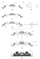
図1は、第1の本実施形態の制御装置を示す断面図である。図2は、図1に示す制御装置の構成と組立て手順である。
図1、図2に示すように、本発明の電子制御装置はマイクロコンピュータ等の電子部品1を実装した制御基板2と、ハウジングケース3と、コネクタ4と、封止樹脂5から構成される。
図2(a)に示すように、ハウジングケース3は電子部品の発熱を電子制御装置の外部に放熱するための放熱フィン6を有するヒートシンク7、電磁ノイズをシールドする電磁シールド部8、及び電子制御装置を車両に固定するための車両固定部9を一体成形してもよい。材料は、高い熱伝導性、シールド性、及び剛性を有した金属材料であることが好ましく、量産性、軽量化、放熱性、コストの観点から、アルミニウム、またはアルミニウム合金であるとよい。このようにヒートシンク7、シールド部8、及び車両固定部9を一体化することで、部品点数が削減できるため、低コスト化、及び生産性の向上を図ることができる。
また、電子部品1からヒートシンク7等ハウジングケース3へ向けて放熱された熱は、車両固定部9がハウジングケース3と一体成形されている場合、車両固定部9を介した車体へ放熱量を向上することが出来る。
コネクタ4は図2(b)に示すように、車両側ハーネスと制御基板2とを接続するための端子10と、端子10を規定のピッチに整列させ、且つ保持するための固定板11から成るコネクタ部組み12を製作する。尚、固定板11は、後述するハウジングケース3への挿入性向上、位置決めを容易とするためのピン13を有し、ピン13の本数は2以上あるとよい。端子10の材料は、導電性、小型化、コストの観点から銅、または銅合金であるとよい。固定板11の材料は、軽量で耐熱性に優れる点から、PBT(Polybutylene Terephthalate)樹脂、PA(Polyamide)66樹脂、PPS(Polyphenylene Sulfide)樹脂を用いるとよい。
続いて、図2(c)に示すように、ハウジングケース3とコネクタ部組み12を組み立てる。その際、コネクタ部組み12のピン13をハウジングケース3の対向する貫通孔に挿入し、固定板11をハウジングケース3に突き当てることで、コネクタ部組み12とハウジングケース3の位置決めを行う。コネクタ部組み12のピン13の直径とハウジングケース3の貫通孔の直径との差を小さく設計することで、平面方向において、コネクタ部組み12の位置ずれを抑制し、端子10とハウジングケースの接触を防ぐことができる。
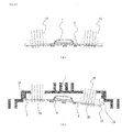
固定部材であるハウジングケース3に対するコネクタ部組み12の位置が決まったら、図2(d)に示すように、ハウジングケース3から突出したピン13の先端を熱かしめにより固定する。図3(a)に熱かしめ部を拡大した断面図を示すが、固定板11を受け台14に置き、予熱した熱かしめジグ15をピン13の先端に押し当て、ピン先端を軟化、熱変形させハウジングケース3に押し当てることで、図3(b)に示すように熱かしめ部を形成する。その際、熱かしめ部のピン直径(Dp)はハウジングケース貫通孔の直径(Dh)よりも大きくするとよい。これにより固定力を増すことが可能となる。
コネクタ部組み12の固定後、図2(e)、(f)に示すように、マイクロコンピュー
タ等の電子部品1を実装した制御基板2をダイカストケース3に組み付ける。その際、外部からの電磁ノイズの影響を受けやすい電子部品、及び電磁ノイズを発生しやすい電子部品、例えば、マイクロコンピュータ、水晶振動子等を制御基板2のハウジングケース3と対向する面に実装する。これにより、電子部品1がハウジングケース3と制御基板2の配線層に囲まれるため、電磁シールド性が向上する。より電磁シールド性を向上させるため、制御基板の配線層のうち一層、または電子部品1が実装される周辺にベタパターンを設けると良い。これにより、ハウジングケース3と対向しない面からの電磁ノイズに対してもシールド性を向上出来る。
タ等の電子部品1を実装した制御基板2をダイカストケース3に組み付ける。その際、外部からの電磁ノイズの影響を受けやすい電子部品、及び電磁ノイズを発生しやすい電子部品、例えば、マイクロコンピュータ、水晶振動子等を制御基板2のハウジングケース3と対向する面に実装する。これにより、電子部品1がハウジングケース3と制御基板2の配線層に囲まれるため、電磁シールド性が向上する。より電磁シールド性を向上させるため、制御基板の配線層のうち一層、または電子部品1が実装される周辺にベタパターンを設けると良い。これにより、ハウジングケース3と対向しない面からの電磁ノイズに対してもシールド性を向上出来る。
制御基板2は、ガラスエポキシ樹脂等をベースとした樹脂配線板を用い、制御基板2に電子部品1を接続する際は、Sn-Cuはんだ、Sn-Ag-Cuはんだ、Sn-Ag-Cu-Biはんだ等の鉛フリーはんだを用いて接続した。制御基板2をハウジングケース3の基板受け部16に設置することで、高さ方向の位置を決め、続いてネジ(非表示)を用いて制御基板2をハウジングケース3に固定する。ネジによる固定点数は3以上とするとよい。コネクタ部組み12の端子10と制御基板2との接続は、端子10が挿入された制御基板2のスルーホール部17を、Sn-Cuはんだ、Sn-Ag-Cuはんだ、Sn-Ag-Cu-Biはんだ等の鉛フリーはんだを用いて接続した。尚、コネクタ4のタイプは、面実装タイプ、プレスフィットタイプであってもよい。
ここで重要なことは、コネクタ部組み12の固定方法であり、コネクタ部組み12をハウジングケース3ではなく、制御基板2に固定する場合、位置決めピン13を制御基板2に挿入することになるために、制御基板2に位置決めピン13用の貫通孔が必要となるため、その分、基板面積が大きくなってしまう。また、コネクタ部組み12の端子10と制御基板2のスルーホール部17をはんだ接合した場合、はんだ接合による熱履歴によりコネクタ部組み12と制御基板2がそれぞれ膨張・収縮することにより、それぞれが変形しようとするが、その膨張・収縮量がコネクタ部組み12と制御基板2とでは異なるために、図4(a)に示すように、破線で示す制御基板2の基の形状に対し、接合後のコネクタ部組み12と制御基板2に反りが発生してしまう。
この反りが生じたコネクタ部組み12と制御基板2をハウジングケース3に固定する場合、図4(b)に示すように、制御基板2の一端31を基板受け部16に置くと、制御基板2の他端において反り量に相当する隙間33が生じる。この状態で制御基板2をハウジングケース3にネジ固定すると、ハウジングケース3の方が制御基板2よりも剛性が大きく、基板受け部16が平らであるために、制御基板2の反りが戻されてしまい、その結果として、コネクタ部組み12の端子10とスルーホール部17のはんだ接合部33、及び制御基板2と電子部品1のはんだ接合部34に応力を残留させ、はんだ接続寿命が低下してしまう。
このような問題が生じることから、コネクタ部組み12の固定方法は、本実施例に述べたとおり、まずコネクタ部組み12をハウジングケース3に固定し、その後に、コネクタ部組み12の端子10と制御基板2のスルーホール部17を接合するとよい。この方法により、コネクタ部組み12と制御基板2の反りを抑制でき、端子10とスルーホール部17接合部への応力発生も抑制可能となる。
このように製作したサブアッシー20を図2(g)に示すように、樹脂封止するための金型にセットする。本実施例では可動型となる上型18にサブアッシーをセットし、上型を可動させ、固定型となる下型19にセットした。樹脂封止後に樹脂5から露出させたいハウジングカバー3のフィン部6、及び車両固定部9は、樹脂成形時に樹脂が流れ込まないようにするため、金型で押さえる構造とした。
封止樹脂5の流動性を確保し、金型内の細部にわたり樹脂充填させるため、金型、サブアッシー、樹脂を予熱しておくとよい。封止樹脂5は熱硬化性のエポキシ樹脂、不飽和ポリエステル樹脂、または、熱可塑性樹脂であってもよい。封止工法としては、トランスファーモールド、圧縮成形、射出成形、ホットメルトで、封止樹脂5の物性値は、線膨張係数が10~30×10-6/℃、熱伝導率が0.5~3W/mKであるとよい。
金型内への樹脂充填完了後、金型内で封止樹脂5を硬化させ、硬化後、金型を開き、樹脂成形品を取り出し、図2(h)に示す電子制御装置を完成させる。
v尚、車両固定部9を除くハウジングケース外周の立ち上がり部22は、封止樹脂5で覆われているようにする。これにより、ハウジングケース3と封止樹脂5の密着面積が増加するため防水・防塩水信頼性を向上でき、更に、ハウジングケース3の膨張・収縮を低減できるため防水・防塩水信頼性、及びはんだ接続信頼性を向上できる。
v尚、車両固定部9を除くハウジングケース外周の立ち上がり部22は、封止樹脂5で覆われているようにする。これにより、ハウジングケース3と封止樹脂5の密着面積が増加するため防水・防塩水信頼性を向上でき、更に、ハウジングケース3の膨張・収縮を低減できるため防水・防塩水信頼性、及びはんだ接続信頼性を向上できる。
更に、コネクタ端子固定板11の熱かしめ部を封止樹脂5で覆うとよい。これにより熱かしめ部の劣化を抑制でき、熱かしめ部からの水、塩水浸入を抑制できる。
最後に、コネクタ4のハウジング21も封止樹脂5にて一体成形するとよい。これにより、コネクタハウジングを別部品で必要としないため、部品点数削減により、コスト低減、生産性の向上が期待される。
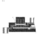
実施例2の形態を実施例1と比較し説明する。実施例1では、固定板11を熱かしめによりハウジングケース3に固定したが、実施例2では、図5に示すように、スナップフィット26で固定する構造とした。
実施例3の形態を実施例1と比較し説明する。実施例1では、固定板11を熱かしめによりハウジングケース3に固定したが、実施例2では、図6に示すように、ネジ27で固定する構造とした。
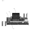
実施例4の形態を実施例1と比較し説明する。実施例1ではコネクタ部組み12をハウジングケース3に固定したが、実施例4では、図7に示すように封止樹脂5とは別体のハウジング付きコネクタ40を用いる。コネクタ40とハウジングケース3との固定にはねじ27などを用いるとよい。
本実施例では、コネクタ40が複数の端子10を固定する板状部を備えており、固定板11の代わりとなってハウジングケース3への位置決めと固定とが可能である。
本実施例では、コネクタ40が複数の端子10を固定する板状部を備えており、固定板11の代わりとなってハウジングケース3への位置決めと固定とが可能である。
以上、本発明に係る制御装置の実施形態について詳述したが、本発明は、前記の実施形態に限定されるものではなく、特許請求の範囲に記載された本発明の精神を逸脱しない範囲で、種々の設計変更を行うことができるものである。
1 電子部品
2 制御基板
3 ハウジングケース
4 コネクタ
5 封止樹脂
5a 放熱フィンを覆う封止樹脂
5b ハウジングケース外周の立ち上がり部を覆う封止樹脂
6 放熱フィン
7 ヒートシンク
8 電磁シールド部
9 車両固定部
10 端子
11 固定板
12 コネクタ部組み
13 ピン
14 受け台
15 熱かしめジグ
16 基板受け部
17 スルーホール部
18 上型
19 下型
20 サブアッシー
21 コネクタのハウジング
22 ハウジングケース外周の立ち上がり部
24 貫通孔
25 金型
26 スナップフィット
27 ネジ
30 電子制御装置
31 制御基板の一端
32 制御基板の他端
33 端子とスルーホール部のはんだ接合部
34 制御基板と電子部品のはんだ接合部
2 制御基板
3 ハウジングケース
4 コネクタ
5 封止樹脂
5a 放熱フィンを覆う封止樹脂
5b ハウジングケース外周の立ち上がり部を覆う封止樹脂
6 放熱フィン
7 ヒートシンク
8 電磁シールド部
9 車両固定部
10 端子
11 固定板
12 コネクタ部組み
13 ピン
14 受け台
15 熱かしめジグ
16 基板受け部
17 スルーホール部
18 上型
19 下型
20 サブアッシー
21 コネクタのハウジング
22 ハウジングケース外周の立ち上がり部
24 貫通孔
25 金型
26 スナップフィット
27 ネジ
30 電子制御装置
31 制御基板の一端
32 制御基板の他端
33 端子とスルーホール部のはんだ接合部
34 制御基板と電子部品のはんだ接合部
Claims (14)
- 電子部品と、
前記電子部品を実装した制御基板と、
前記制御基板を封止する封止樹脂と、
少なくとも一部が前記封止樹脂によって封止される固定部材と、
前記制御基板と外部機器との電気接続を行うための端子と、
前記端子を前記固定部材に対して位置決めして固定する固定板と、を備えることを特徴とする電子制御装置。 - 前記端子は複数の金属製端子を備え、前記封止樹脂が前記端子を覆い、外部コネクタと嵌合するコネクタハウジングを一体に形成していることを特徴とする請求項1に記載の電子制御装置。
- 前記固定部材は金属製の板状部材であり、少なくとも一部が前記封止樹脂から露出する露出部を備え、
前記露出部は、前記電子部品からの発熱を外部へ放熱するヒートシンク部、または車体に固定するための車体固定部を備えることを特徴とする請求項2記載の電子制御装置。 - 前記端子は複数の金属製端子を備え、前記固定板と前記固定部材とを垂直に貫通するように設けられていることを特徴とする請求項3記載の電子制御装置。
- 前記固定板は、前記固定部材に向かって伸びるようにピンが設けられ、
前記ピンは、前記固定部材の前記固定板と対向する部分に設けられた貫通孔に挿入されており、
前記固定部材に熱かしめ固定されていることを特徴とする請求項3または4いずれか一項に記載の電子制御装置。 - 前記固定板の材料は熱可塑性樹脂であることを特徴とする請求項2から5いずれか一項に記載の電子制御装置。
- 前記熱かしめ固定されている箇所は、前記封止樹脂にて覆われていることを特徴とする請求項5に記載の電子制御装置。
- 前記固定板は、前記固定部材に少なくとも2箇所で熱かしめ固定されていることを特徴とする請求項7に記載の電子制御装置。
- 熱かしめ後の前記ピンの先端は前記固定部材の貫通孔から突出し、ピン先端直径が前記貫通孔の直径よりも大きいことを特徴とする請求項5,7または8いずれか一項に記載の電子制御装置。
- 前記封止樹脂の材料は、熱硬化性樹脂であることを特徴とする請求項2から9いずれか一項に記載の電子制御装置。
- 前記固定板が、スナップフィットにて前記固定部材に固定されていることを特徴とする請求項2から10いずれか一項に記載の電子制御装置。
- 前記固定板が、ねじにて前記固定部材に固定されていることを特徴とする請求項2から11いずれか一項に記載の電子制御装置。
- 前記端子は複数の金属製端子を備え、前記固定板は、前記端子を覆って外部コネクタと嵌合するコネクタハウジングの一部であり、前記固定板は前記封止樹脂と別体に形成されていることを特徴とする請求項1記載の電子制御装置。
- 複数の金属端子が保持された固定板を固定部材に対して固定にする行程と、
前記複数の金属端子が前記固定板により前記固定部材に固定された後に、電子部品を実装した制御基板と前記複数の金属端子とを電気的に接続する行程と、
前記複数の金属端子の一部と前記制御基板と前記固定部材の少なくとも一部とを封止樹脂で封止する行程と、を備える電子制御装置の製造方法。
Priority Applications (4)
| Application Number | Priority Date | Filing Date | Title |
|---|---|---|---|
| US15/763,713 US10517181B2 (en) | 2015-09-29 | 2016-08-05 | Electronic control device and manufacturing method for same |
| EP16850905.7A EP3358919B1 (en) | 2015-09-29 | 2016-08-05 | Electronic control device and manufacturing method for same |
| CN201680056543.2A CN108141970B (zh) | 2015-09-29 | 2016-08-05 | 电子控制装置及其制造方法 |
| JP2017542991A JP6561129B2 (ja) | 2015-09-29 | 2016-08-05 | 電子制御装置またはその製造方法 |
Applications Claiming Priority (2)
| Application Number | Priority Date | Filing Date | Title |
|---|---|---|---|
| JP2015190620 | 2015-09-29 | ||
| JP2015-190620 | 2015-09-29 |
Publications (1)
| Publication Number | Publication Date |
|---|---|
| WO2017056728A1 true WO2017056728A1 (ja) | 2017-04-06 |
Family
ID=58423447
Family Applications (1)
| Application Number | Title | Priority Date | Filing Date |
|---|---|---|---|
| PCT/JP2016/073033 Ceased WO2017056728A1 (ja) | 2015-09-29 | 2016-08-05 | 電子制御装置またはその製造方法 |
Country Status (5)
| Country | Link |
|---|---|
| US (1) | US10517181B2 (ja) |
| EP (1) | EP3358919B1 (ja) |
| JP (1) | JP6561129B2 (ja) |
| CN (1) | CN108141970B (ja) |
| WO (1) | WO2017056728A1 (ja) |
Cited By (5)
| Publication number | Priority date | Publication date | Assignee | Title |
|---|---|---|---|---|
| JP2020136293A (ja) * | 2019-02-13 | 2020-08-31 | 富士電機株式会社 | 半導体装置及びその製造方法 |
| WO2021025146A1 (ja) | 2019-08-08 | 2021-02-11 | 住友ベークライト株式会社 | 封止樹脂組成物、および電子部品 |
| WO2023162975A1 (ja) | 2022-02-28 | 2023-08-31 | 住友ベークライト株式会社 | 封止用樹脂組成物および半導体装置 |
| WO2023238605A1 (ja) * | 2022-06-09 | 2023-12-14 | カヤバ株式会社 | 電子部品ユニットおよび電子部品ユニットの製造方法 |
| JP7627561B2 (ja) | 2020-10-12 | 2025-02-06 | 新電元工業株式会社 | 電子装置 |
Families Citing this family (4)
| Publication number | Priority date | Publication date | Assignee | Title |
|---|---|---|---|---|
| US9839146B2 (en) | 2015-10-20 | 2017-12-05 | Cree, Inc. | High voltage power module |
| USD908632S1 (en) * | 2018-09-17 | 2021-01-26 | Cree Fayetteville, Inc. | Power module |
| JP7168483B2 (ja) * | 2019-02-12 | 2022-11-09 | アルプスアルパイン株式会社 | スイッチ装置及びスイッチ装置の製造方法 |
| JP7405588B2 (ja) * | 2019-12-11 | 2023-12-26 | ファナック株式会社 | ハウジング及び関節機構 |
Citations (3)
| Publication number | Priority date | Publication date | Assignee | Title |
|---|---|---|---|---|
| JP2006190725A (ja) * | 2005-01-04 | 2006-07-20 | Hitachi Ltd | 樹脂封止型エンジンコントロール装置並びにその製造方法 |
| JP2014015080A (ja) * | 2012-07-06 | 2014-01-30 | Hitachi Automotive Systems Ltd | 車載用電子制御装置 |
| JP2014053382A (ja) * | 2012-09-05 | 2014-03-20 | Denso Corp | 筺体及び電子装置 |
Family Cites Families (23)
| Publication number | Priority date | Publication date | Assignee | Title |
|---|---|---|---|---|
| CN1123515A (zh) * | 1994-11-24 | 1996-05-29 | 三菱电机株式会社 | 树脂模压的电子电路装置 |
| JP3290909B2 (ja) * | 1997-02-19 | 2002-06-10 | 矢崎総業株式会社 | 基板用コネクタ |
| US6180045B1 (en) * | 1998-05-20 | 2001-01-30 | Delco Electronics Corporation | Method of forming an overmolded electronic assembly |
| DE10017335B4 (de) * | 2000-04-07 | 2011-03-10 | Conti Temic Microelectronic Gmbh | Elektronische Baugruppe |
| US6307749B1 (en) | 2000-10-23 | 2001-10-23 | Delphi Technologies, Inc. | Overmolded electronic module with underfilled surface-mount components |
| JP2003243066A (ja) * | 2002-02-19 | 2003-08-29 | Denso Corp | 電子装置 |
| JP4015590B2 (ja) | 2003-06-04 | 2007-11-28 | 住友電装株式会社 | ケースのシール構造、及びその組付方法 |
| CN100408380C (zh) * | 2003-08-01 | 2008-08-06 | 西门子公司 | 电子单元以及用于制造电子单元的方法 |
| US7492600B2 (en) * | 2003-11-14 | 2009-02-17 | Tyco Electronics Corporation | Sealed header and method of making |
| US7149089B2 (en) * | 2004-01-14 | 2006-12-12 | Delphi Technologies, Inc. | Electrical assembly |
| JP2006032490A (ja) * | 2004-07-13 | 2006-02-02 | Hitachi Ltd | エンジン制御回路装置 |
| JP4475160B2 (ja) * | 2005-04-13 | 2010-06-09 | 株式会社デンソー | 電子装置の製造方法 |
| US7473585B2 (en) * | 2005-06-13 | 2009-01-06 | Delphi Technologies, Inc. | Technique for manufacturing an overmolded electronic assembly |
| JP4741969B2 (ja) | 2006-03-31 | 2011-08-10 | 日立オートモティブシステムズ株式会社 | 自動車の電気電子モジュールおよびその取り付け方法 |
| WO2008005945A2 (en) * | 2006-06-30 | 2008-01-10 | Molex Incorporated | Compliant pin control module and method for making the same |
| JP5062107B2 (ja) * | 2008-09-01 | 2012-10-31 | 株式会社デンソー | 電子装置の筐体構造 |
| JP5103409B2 (ja) * | 2009-01-20 | 2012-12-19 | 日立オートモティブシステムズ株式会社 | 電気・電子モジュール及びその製造方法 |
| DE102010002765A1 (de) * | 2010-03-11 | 2011-09-15 | Robert Bosch Gmbh | Gehäusegrundelement eines mehrteiligen Gehäuses und Verfahren zur Montage eines Gehäuses |
| DE102012204145A1 (de) * | 2012-03-16 | 2013-09-19 | Continental Automotive Gmbh | Gehäuseblende zur Aufnahme von Steckermodulen |
| JP2013243272A (ja) * | 2012-05-22 | 2013-12-05 | Sumitomo Electric Ind Ltd | 炭化珪素半導体装置およびその製造方法 |
| US9480143B2 (en) * | 2013-10-09 | 2016-10-25 | Uusi, Llc | Motor control device |
| JP5943985B2 (ja) * | 2014-10-30 | 2016-07-05 | 三菱電機株式会社 | 電子制御装置 |
| WO2017038316A1 (ja) * | 2015-09-04 | 2017-03-09 | 日立オートモティブシステムズ株式会社 | 車載制御装置 |
-
2016
- 2016-08-05 JP JP2017542991A patent/JP6561129B2/ja active Active
- 2016-08-05 CN CN201680056543.2A patent/CN108141970B/zh active Active
- 2016-08-05 US US15/763,713 patent/US10517181B2/en active Active
- 2016-08-05 WO PCT/JP2016/073033 patent/WO2017056728A1/ja not_active Ceased
- 2016-08-05 EP EP16850905.7A patent/EP3358919B1/en active Active
Patent Citations (3)
| Publication number | Priority date | Publication date | Assignee | Title |
|---|---|---|---|---|
| JP2006190725A (ja) * | 2005-01-04 | 2006-07-20 | Hitachi Ltd | 樹脂封止型エンジンコントロール装置並びにその製造方法 |
| JP2014015080A (ja) * | 2012-07-06 | 2014-01-30 | Hitachi Automotive Systems Ltd | 車載用電子制御装置 |
| JP2014053382A (ja) * | 2012-09-05 | 2014-03-20 | Denso Corp | 筺体及び電子装置 |
Non-Patent Citations (1)
| Title |
|---|
| See also references of EP3358919A4 * |
Cited By (7)
| Publication number | Priority date | Publication date | Assignee | Title |
|---|---|---|---|---|
| JP2020136293A (ja) * | 2019-02-13 | 2020-08-31 | 富士電機株式会社 | 半導体装置及びその製造方法 |
| JP7310161B2 (ja) | 2019-02-13 | 2023-07-19 | 富士電機株式会社 | 半導体装置及びその製造方法 |
| WO2021025146A1 (ja) | 2019-08-08 | 2021-02-11 | 住友ベークライト株式会社 | 封止樹脂組成物、および電子部品 |
| JP7627561B2 (ja) | 2020-10-12 | 2025-02-06 | 新電元工業株式会社 | 電子装置 |
| WO2023162975A1 (ja) | 2022-02-28 | 2023-08-31 | 住友ベークライト株式会社 | 封止用樹脂組成物および半導体装置 |
| KR20240154052A (ko) | 2022-02-28 | 2024-10-24 | 스미또모 베이크라이트 가부시키가이샤 | 봉지용 수지 조성물 및 반도체 장치 |
| WO2023238605A1 (ja) * | 2022-06-09 | 2023-12-14 | カヤバ株式会社 | 電子部品ユニットおよび電子部品ユニットの製造方法 |
Also Published As
| Publication number | Publication date |
|---|---|
| JPWO2017056728A1 (ja) | 2018-03-01 |
| CN108141970A (zh) | 2018-06-08 |
| EP3358919A1 (en) | 2018-08-08 |
| US20180288888A1 (en) | 2018-10-04 |
| EP3358919A4 (en) | 2019-05-15 |
| EP3358919B1 (en) | 2022-07-20 |
| CN108141970B (zh) | 2020-06-09 |
| JP6561129B2 (ja) | 2019-08-14 |
| US10517181B2 (en) | 2019-12-24 |
Similar Documents
| Publication | Publication Date | Title |
|---|---|---|
| JP6561129B2 (ja) | 電子制御装置またはその製造方法 | |
| JP6582052B2 (ja) | 電子制御装置または車載電子制御装置の製造方法 | |
| US10829064B2 (en) | Electronic control device | |
| WO2017056727A1 (ja) | 電子制御装置 | |
| WO2014119379A1 (ja) | 車載用電子モジュール | |
| JP2003124662A (ja) | 車載電子機器 | |
| JP4841592B2 (ja) | 制御装置 | |
| CN112689889B (zh) | 电子控制装置以及电子控制装置的制造方法 | |
| CN109644569B (zh) | 控制器单元和将其接线插脚固定在其电路板元件中的方法 | |
| WO2018116710A1 (ja) | 電子制御装置 | |
| JP4741969B2 (ja) | 自動車の電気電子モジュールおよびその取り付け方法 | |
| WO2016084537A1 (ja) | 電子制御装置 | |
| JP6277061B2 (ja) | 電子制御装置 | |
| JP6685252B2 (ja) | 電子制御装置 | |
| JP4864742B2 (ja) | モジュール装置 | |
| JP2015216061A (ja) | 電子制御装置 | |
| JP2009049109A (ja) | モジュール装置 |
Legal Events
| Date | Code | Title | Description |
|---|---|---|---|
| 121 | Ep: the epo has been informed by wipo that ep was designated in this application |
Ref document number: 16850905 Country of ref document: EP Kind code of ref document: A1 |
|
| ENP | Entry into the national phase |
Ref document number: 2017542991 Country of ref document: JP Kind code of ref document: A |
|
| WWE | Wipo information: entry into national phase |
Ref document number: 15763713 Country of ref document: US |
|
| NENP | Non-entry into the national phase |
Ref country code: DE |