WO2017047815A1 - 発光装置 - Google Patents
発光装置 Download PDFInfo
- Publication number
- WO2017047815A1 WO2017047815A1 PCT/JP2016/077736 JP2016077736W WO2017047815A1 WO 2017047815 A1 WO2017047815 A1 WO 2017047815A1 JP 2016077736 W JP2016077736 W JP 2016077736W WO 2017047815 A1 WO2017047815 A1 WO 2017047815A1
- Authority
- WO
- WIPO (PCT)
- Prior art keywords
- light
- emitting device
- led element
- led
- light emitting
- Prior art date
- Legal status (The legal status is an assumption and is not a legal conclusion. Google has not performed a legal analysis and makes no representation as to the accuracy of the status listed.)
- Ceased
Links
Images






Classifications
-
- H—ELECTRICITY
- H10—SEMICONDUCTOR DEVICES; ELECTRIC SOLID-STATE DEVICES NOT OTHERWISE PROVIDED FOR
- H10W—GENERIC PACKAGES, INTERCONNECTIONS, CONNECTORS OR OTHER CONSTRUCTIONAL DETAILS OF DEVICES COVERED BY CLASS H10
- H10W90/00—Package configurations
-
- G—PHYSICS
- G02—OPTICS
- G02B—OPTICAL ELEMENTS, SYSTEMS OR APPARATUS
- G02B5/00—Optical elements other than lenses
- G02B5/02—Diffusing elements; Afocal elements
-
- H—ELECTRICITY
- H10—SEMICONDUCTOR DEVICES; ELECTRIC SOLID-STATE DEVICES NOT OTHERWISE PROVIDED FOR
- H10H—INORGANIC LIGHT-EMITTING SEMICONDUCTOR DEVICES HAVING POTENTIAL BARRIERS
- H10H20/00—Individual inorganic light-emitting semiconductor devices having potential barriers, e.g. light-emitting diodes [LED]
- H10H20/80—Constructional details
- H10H20/85—Packages
- H10H20/8506—Containers
-
- H—ELECTRICITY
- H10—SEMICONDUCTOR DEVICES; ELECTRIC SOLID-STATE DEVICES NOT OTHERWISE PROVIDED FOR
- H10H—INORGANIC LIGHT-EMITTING SEMICONDUCTOR DEVICES HAVING POTENTIAL BARRIERS
- H10H20/00—Individual inorganic light-emitting semiconductor devices having potential barriers, e.g. light-emitting diodes [LED]
- H10H20/80—Constructional details
- H10H20/85—Packages
- H10H20/852—Encapsulations
-
- H—ELECTRICITY
- H10—SEMICONDUCTOR DEVICES; ELECTRIC SOLID-STATE DEVICES NOT OTHERWISE PROVIDED FOR
- H10H—INORGANIC LIGHT-EMITTING SEMICONDUCTOR DEVICES HAVING POTENTIAL BARRIERS
- H10H20/00—Individual inorganic light-emitting semiconductor devices having potential barriers, e.g. light-emitting diodes [LED]
- H10H20/01—Manufacture or treatment
- H10H20/036—Manufacture or treatment of packages
-
- H—ELECTRICITY
- H10—SEMICONDUCTOR DEVICES; ELECTRIC SOLID-STATE DEVICES NOT OTHERWISE PROVIDED FOR
- H10H—INORGANIC LIGHT-EMITTING SEMICONDUCTOR DEVICES HAVING POTENTIAL BARRIERS
- H10H20/00—Individual inorganic light-emitting semiconductor devices having potential barriers, e.g. light-emitting diodes [LED]
- H10H20/01—Manufacture or treatment
- H10H20/036—Manufacture or treatment of packages
- H10H20/0361—Manufacture or treatment of packages of wavelength conversion means
-
- H—ELECTRICITY
- H10—SEMICONDUCTOR DEVICES; ELECTRIC SOLID-STATE DEVICES NOT OTHERWISE PROVIDED FOR
- H10H—INORGANIC LIGHT-EMITTING SEMICONDUCTOR DEVICES HAVING POTENTIAL BARRIERS
- H10H20/00—Individual inorganic light-emitting semiconductor devices having potential barriers, e.g. light-emitting diodes [LED]
- H10H20/01—Manufacture or treatment
- H10H20/036—Manufacture or treatment of packages
- H10H20/0362—Manufacture or treatment of packages of encapsulations
-
- H—ELECTRICITY
- H10—SEMICONDUCTOR DEVICES; ELECTRIC SOLID-STATE DEVICES NOT OTHERWISE PROVIDED FOR
- H10H—INORGANIC LIGHT-EMITTING SEMICONDUCTOR DEVICES HAVING POTENTIAL BARRIERS
- H10H20/00—Individual inorganic light-emitting semiconductor devices having potential barriers, e.g. light-emitting diodes [LED]
- H10H20/80—Constructional details
- H10H20/85—Packages
- H10H20/851—Wavelength conversion means
- H10H20/8514—Wavelength conversion means characterised by their shape, e.g. plate or foil
-
- H—ELECTRICITY
- H10—SEMICONDUCTOR DEVICES; ELECTRIC SOLID-STATE DEVICES NOT OTHERWISE PROVIDED FOR
- H10H—INORGANIC LIGHT-EMITTING SEMICONDUCTOR DEVICES HAVING POTENTIAL BARRIERS
- H10H20/00—Individual inorganic light-emitting semiconductor devices having potential barriers, e.g. light-emitting diodes [LED]
- H10H20/80—Constructional details
- H10H20/85—Packages
- H10H20/851—Wavelength conversion means
- H10H20/8515—Wavelength conversion means not being in contact with the bodies
-
- H—ELECTRICITY
- H10—SEMICONDUCTOR DEVICES; ELECTRIC SOLID-STATE DEVICES NOT OTHERWISE PROVIDED FOR
- H10H—INORGANIC LIGHT-EMITTING SEMICONDUCTOR DEVICES HAVING POTENTIAL BARRIERS
- H10H20/00—Individual inorganic light-emitting semiconductor devices having potential barriers, e.g. light-emitting diodes [LED]
- H10H20/80—Constructional details
- H10H20/85—Packages
- H10H20/852—Encapsulations
- H10H20/854—Encapsulations characterised by their material, e.g. epoxy or silicone resins
-
- H—ELECTRICITY
- H10—SEMICONDUCTOR DEVICES; ELECTRIC SOLID-STATE DEVICES NOT OTHERWISE PROVIDED FOR
- H10H—INORGANIC LIGHT-EMITTING SEMICONDUCTOR DEVICES HAVING POTENTIAL BARRIERS
- H10H20/00—Individual inorganic light-emitting semiconductor devices having potential barriers, e.g. light-emitting diodes [LED]
- H10H20/80—Constructional details
- H10H20/85—Packages
- H10H20/855—Optical field-shaping means, e.g. lenses
- H10H20/856—Reflecting means
-
- H—ELECTRICITY
- H10—SEMICONDUCTOR DEVICES; ELECTRIC SOLID-STATE DEVICES NOT OTHERWISE PROVIDED FOR
- H10H—INORGANIC LIGHT-EMITTING SEMICONDUCTOR DEVICES HAVING POTENTIAL BARRIERS
- H10H20/00—Individual inorganic light-emitting semiconductor devices having potential barriers, e.g. light-emitting diodes [LED]
- H10H20/80—Constructional details
- H10H20/882—Scattering means
Definitions
- the present invention relates to a light emitting device.
- Patent Document 1 a green light emitting element, a blue light emitting element, and a red light emitting element mounted on a chip substrate as light emitters, and a light emitting body that is disposed on the chip substrate so as to surround the light emitter, and has an upper surface and a side wall.
- a reflection frame having an opening in the part, a reflection surface formed on the inner peripheral surface of the side wall of the reflection frame, a light-transmitting resin body formed in the reflection frame and having the opening on the side wall side as a light emission surface;
- a light-emitting diode chip including a reflective film covering a light-transmitting resin body exposed on the upper surface of the reflective frame.
- Patent Document 2 includes a red LED element, a green LED element, and a blue LED element, and a reflective cover for reflecting light emitted from the LED without leaking to the outside and emitting light in a direction substantially parallel to the LED installation surface.
- An LED low profile light source device is described.
- Patent Document 3 discloses an LED light emitting device in which a red LED, a green LED, and a blue LED and a white LED formed by coating a blue LED with a resin mixed with a phosphor are mounted on a mounting substrate at different heights. Is described.
- Patent Document 4 has a long-wavelength blue LED element sealed with a sealing member containing a phosphor that emits yellow excitation light, and a red LED element whose upper part is covered with a light-shielding film. A white LED that emits white illumination light to the outside is described.
- an object of the present invention is to provide a light emitting device that improves color mixing and light emission efficiency while realizing high color rendering white light by four types of LED elements that respectively emit red light, green light, blue light, and white light. Is to provide.
- a fourth LED element that is arranged farther from the phosphor layer than the LED element and emits blue light, a substrate on which the first to fourth LED elements are mounted on the same mounting surface, and an outer periphery of the substrate
- a resin frame that surrounds at least a portion, a sealing resin that is filled on a substrate in the resin frame and seals the first to fourth LED elements, and a sealing resin that is a surface opposite to the mounting surface
- a light shielding member disposed on the upper surface and covering at least the first LED element.
- a scattering agent that diffuses light is dispersed and mixed in the sealing resin.
- the resin frame preferably has an inner white resin layer that reflects light toward the sealing resin side and an outer black resin layer that prevents light from being transmitted to the outside.
- the light shielding member preferably has an inner white sheet that reflects light toward the sealing resin side and an outer black sheet that prevents light from being transmitted to the outside.
- the light shielding member covers the entire top surface of the sealing resin
- the resin frame has an exit port for the emitted light from the first to fourth LED elements, and the emitted light passes from the exit port to the mounting surface.
- the light is emitted in a direction parallel to.
- the light shielding member covers the upper side of the first LED element, the resin frame surrounds the entire outer periphery of the substrate, and the light emitted from the first to fourth LED elements is the second to fourth It is preferable that the light is emitted from above the LED element in a direction perpendicular to the mounting surface.
- the first to fourth LED elements are preferably arranged in a straight line in this order on the mounting surface.
- the phosphor layer divides the sealing resin into two parts between the first LED element and the second LED element, and the second LED element is made to be the first LED element rather than the phosphor layer. It is preferable to arrange on the near side.
- the second to fourth LED elements are preferably arranged in a triangular shape.
- the third and fourth LED elements are preferably transparent elements that transmit white light and red light, and the second LED elements are preferably opaque elements that do not transmit blue light.
- the above light emitting device it is possible to improve color mixing and light emission efficiency while realizing high color rendering white light by four types of LED elements that respectively emit red light, green light, blue light, and white light. .
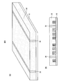
- FIG. 1 is a perspective view of a light emitting device 1.
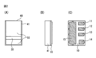
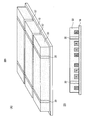
- FIG. FIGS. 4A to 4C are a top view, a side view, and a bottom view of the light-emitting device 1.
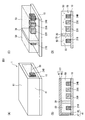
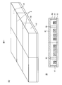
- FIG. (A) to (D) are diagrams for explaining the structure of the light emitting device 1.
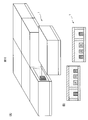
- (A) And (B) is a figure for demonstrating the structure of the light-emitting device 1.
- FIG. (A) And (B) is a figure which shows the manufacturing process of the light-emitting device 1.
- FIG. (A) And (B) is a figure which shows the manufacturing process of the light-emitting device 1.
- FIG. (A) And (B) is a figure which shows the manufacturing process of the light-emitting device 1.
- FIG. (A) And (B) is a figure which shows the manufacturing process of the light-emitting device 1.
- FIG. (A) And (B) is a figure which shows the manufacturing process of the light-emitting device 1.
- FIG. (A) And (B) is a figure which shows the manufacturing process of the light-emitting device 1.
- FIG. (A) And (B) is a figure which shows the manufacturing process of the light-emitting device 1.
- FIG. (A) And (B) is a figure which shows the manufacturing process of the light-emitting device 1.
- FIG. (A) And (B) is a figure which shows the manufacturing process of the light-emitting device 1.
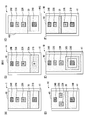
- FIG. (A) to (F) are top views of the light emitting devices 1, 1A, 1B, 1C, 1D, and 1E.
- (A) to (D) are diagrams for explaining the structure of the light emitting device 2.
- FIG. (A) And (B) is a figure for demonstrating the structure of the light-emitting device 2.
- FIG. (A) to (E) are top views of the light emitting devices 2, 2A, 2C, 2D, and 2E.
- (A)-(D) are top views of other light emitting devices 1F, 1G, 2F, 2G.
- (A) And (B) is a figure for demonstrating the structure of the light-emitting device 3.
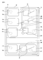
- FIG. 3 is a plan view showing the arrangement of circuit patterns 16a to 16f and LED elements 21B, 22R, 23G, and 24B on a substrate 10.
- FIG. 1 is a perspective view of the light emitting device 1.
- 2A to 2C are a top view, a side view, and a bottom view of the light-emitting device 1, respectively.
- FIGS. 3A to 4B are views for explaining the structure of the light-emitting device 1.
- the light emitting device 1 includes a substrate 10, four LED elements 21B, 22R, 23G, and 24B, a phosphor layer 30, a resin frame 41, a sealing resin 50, and a light shielding member 61.
- the light emitting device 1 emits white (W) light using three LED elements 22R, 23G, and 24B that respectively emit red (R) light, green (G) light, and blue (B) light, and the phosphor layer 30.
- the LED element 21B that emits light realizes high color rendering white light.
- the three side surfaces and the upper surface of the light emitting device 1 are covered with a resin frame 41 and a light shielding member 61.
- One side surface that is not covered by the resin frame 41 is an emission port 48 of the light emitting device 1.
- the light emitting device 1 is shown by an arrow L in FIGS. 4 (A) and 4 (B). To emit light.
- the light-emitting device 1 is a side-emitting LED package that can be used as an illumination light source or a light source for a backlight.
- FIG. 1 shows the light emitting device 1 from which the light shielding member 61 is removed.
- FIG. 1 and FIG. 2 (A) the description of the LED elements 21B, 22R, 23G, and 24B is omitted.
- FIG. 3A is a perspective view showing the light emitting device 1 to which the resin frame 41 and the light shielding member 61 are attached
- FIG. 3B is a longitudinal sectional view of FIG. 3C is a perspective view showing the light emitting device 1 with the resin frame 41 and the light shielding member 61 removed
- FIG. 3D is a longitudinal sectional view of FIG. 4A is a top view of the light-emitting device 1 with the light shielding member 61 removed
- FIG. 4B is a longitudinal sectional view of FIG. 4A.
- FIG. 19 is a plan view showing the arrangement of the circuit patterns 16a to 16f and the LED elements 21B, 22R, 23G, and 24B on the substrate 10.
- the substrate 10 is a substrate on which the LED elements 21B, 22R, 23G, and 24B are mounted on the same mounting surface that is the upper surface thereof.
- the substrate 10 is an insulating substrate such as a glass epoxy substrate, a BT resin substrate, a ceramic substrate, or a metal core substrate. is there.
- a glass epoxy substrate such as a glass epoxy substrate, a BT resin substrate, a ceramic substrate, or a metal core substrate. is there.
- FIG. 2C on the bottom surface of the substrate 10, five electrodes 11 to 15 for supplying power to the LED elements 21B, 22R, 23G, and 24B are provided.
- substantially rectangular circuit patterns 16a to 16d are provided on the top surface of the substrate 10 at positions corresponding to the bottom electrodes 11 to 14, respectively, and positions corresponding to the bottom surface electrodes 15 are provided.
- circuit patterns 16e and 16f are provided.
- the circuit patterns 16a to 16c and 16e are arranged on the side closer to the emission port 48 than the phosphor layer 30, and the circuit patterns 16d and 16f are arranged on the side farther from the emission port 48 than the phosphor layer 30, respectively.
- the electrodes 11 to 14 and the circuit patterns 16a to 16d are electrically connected through the through electrodes 17a to 17d, respectively, and the electrode 15 and the circuit patterns 16e and 16f are electrically connected to each other through the through electrodes 17e and 17f.
- the electrodes 11 to 14 are anode electrodes corresponding to the LED elements 21B, 22R, 23G, and 24B, respectively, and the electrode 15 is a cathode electrode common to the LED elements 21B, 22R, 23G, and 24B.
- the substrate 10 may be provided with four cathode electrodes respectively corresponding to the four LED elements and one anode electrode common to the four LED elements, or each of the LED elements 21B, 22R, 23G, 24B. A total of eight electrodes may be provided.
- the electrodes (element electrodes) of the LED elements 21B, 22R, 23G, and 24B are electrically connected to the circuit patterns 16a to 16f via a conductive adhesive material such as Ag paste or a wire by wire bonding.
- a conductive adhesive material such as Ag paste or a wire by wire bonding.
- the LED element 21 ⁇ / b> B is mounted on the circuit pattern 16 f, and its element electrode is connected to the circuit patterns 16 d and 16 f by wires 25.
- the LED element 22R is mounted on the circuit pattern 16e, and its element electrode is connected to the circuit pattern 16c by a wire 25.
- the LED element 23G is mounted on the circuit pattern 16e, and its element electrode is connected to the circuit patterns 16b and 16e by wires 25.
- the LED element 24B is mounted on the circuit pattern 16e, and its element electrode is connected to the circuit patterns 16a and 16e by wires 25.
- the LED element 21B is an example of a first LED element, for example, a blue LED element that emits blue light having an emission wavelength band of about 450 to 460 nm.
- the phosphor layer 30 is a resin layer containing the phosphor 35 and is provided so as to divide the sealing resin 50 between the LED element 21B and the LED element 22R. Yes.
- the phosphor 35 for example, a yellow phosphor such as YAG (yttrium aluminum garnet) is used.
- the LED element 21B emits white light by a combination of blue light and yellow light generated by exciting the yellow phosphor in the phosphor layer 30 with the blue light.
- the phosphor layer 30 may contain a plurality of types of phosphors such as a green phosphor and a red phosphor instead of the yellow phosphor.
- the green phosphor is a particulate phosphor material such as (BaSr) 2 SiO 4 : Eu 2+ that absorbs blue light emitted from the LED element 21B and converts the wavelength into green light.
- the red phosphor is a particulate phosphor material such as CaAlSiN 3 : Eu 2+ that absorbs blue light emitted from the LED element 21B and converts the wavelength into red light.
- the LED element 21B emits white light obtained by mixing blue light and green light and red light obtained by exciting the green phosphor and the red phosphor with the blue light.
- the LED element 21B and the phosphor layer 30 instead of the LED element 21B and the phosphor layer 30, as the first LED element and the phosphor layer, for example, the upper surface and the side surface are covered with a resin layer containing a yellow phosphor, and white light is emitted alone.
- a blue LED element may be provided.
- the LED element 22R is an example of a second LED element, for example, a red LED element that emits red light having an emission wavelength band of about 620 to 660 nm.
- the LED element 23G is an example of a third LED element, for example, a green LED element that emits green light having an emission wavelength band of about 510 to 530 nm.
- the LED element 24B is an example of a fourth LED element.
- the LED element 24B is a blue LED element that emits blue light having an emission wavelength band of about 450 to 460 nm.
- the LED elements 21B and 24B may have the same characteristics, or may have different characteristics.
- the four LED elements can be driven independently. Control of the current value of each LED element is complicated when it is attempted to adjust the color tone using only the three LED elements of RGB, but the light emitting device 1 further includes the white (W) LED element 21B, and thus the LED element 22R. , 23G, and 24B and the LED element 21B can emit light, so that the color can be adjusted based on white light. For example, if two LED elements 21B and 22R are made to emit light, reddish white light can be easily obtained, and if two LED elements 21B and 24B are made to emit light, bluish white light can be easily obtained. Therefore, the control of the current value of the LED element is simplified.
- blue light excites the yellow phosphor
- the emitted light from the blue LED element excites the yellow phosphor.
- white light is generated, and the amount of blue light may be reduced.
- the green light also slightly excites the yellow phosphor, the amount of green light can be reduced even when the green LED element is mounted near the white LED element.
- the red light does not excite the yellow phosphor, even if the red LED element is mounted near the white LED element, the amount of red light does not decrease.
- the blue LED element needs to be separated from the phosphor layer of the white LED element, and the green LED element is also separated from the phosphor layer.
- the red LED element may be arranged anywhere.
- the LED elements 22 ⁇ / b> R, 23 ⁇ / b> G, and 24 ⁇ / b> B are more than the phosphor layer 30 so that the LED element 24 ⁇ / b> B is farthest from the phosphor layer 30 and the LED element 22 ⁇ / b> R is closest to the phosphor layer 30.
- the LED element 21B is mounted linearly in front of the light emission path (light path).
- the LED element 24B is disposed farther from the phosphor layer 30 than the LED elements 22R and 23G on the opposite side of the LED element 21B across the phosphor layer 30, and the LED elements 21B, 22R, 23G, 24B are arranged in a straight line in this order on the mounting surface of the substrate 10.
- the LED elements 23G and 24B are, for example, transparent elements configured based on sapphire. If the LED elements 23G, 24B are transparent elements that transmit white light and red light, even if the LED elements 22R, 23G, 24B are mounted in a straight line toward the emission port 48, for example, by the LED element 22R Since red light is not blocked by the LED elements 23G and 24B, the color mixing property is improved.
- the LED element 22R is preferably an opaque element. If the LED element 22R is an opaque element that does not transmit blue light, the blue light emitted from the LED element 24B toward the phosphor layer 30 is blocked by the LED element 22R, so that excitation light from the phosphor layer 30 is not emitted. It will not occur unnecessarily.
- the resin frame 41 is a resin member that surrounds the three outer peripheral surfaces of the substrate 10 except for one surface where the emission port 48 of the light emitting device 1 is provided.
- the resin frame 41 has an emission port 48 for emitted light from the LED elements 21B, 22R, 23G, and 24B. The emitted light is emitted from the emission port 48 in a direction parallel to the mounting surface of the substrate 10.
- the resin frame 41 includes an inner white resin layer 46 that reflects the emitted light from the LED elements 21B, 22R, 23G, and 24B to the sealing resin 50 side, and the light emitted to the outside. It is preferable to have a two-layer structure with an outer black resin layer 47 that prevents transmission.
- the white resin layer 46 since the white resin layer 46 is provided, the light from each LED element is reflected to the inside of the light emitting device 1, so that the color mixing property is improved.
- the white resin layer 46 alone may transmit light from the side surface of the light emitting device 1 through the resin frame 41.
- the black resin layer 47 is further outside the white resin layer 46. As a result, light is less likely to leak to the outside, so that the light emission efficiency is improved.
- the sealing resin 50 is filled on the substrate 10 in the resin frame 41, and integrally covers and protects (seals) the LED elements 21B, 22R, 23G, and 24B.
- a colorless and transparent resin such as an epoxy resin or a silicone resin may be used.
- the sealing resin 50 is preferably mixed with a scattering agent 55 such as glass particles that diffuses the light emitted from the LED elements 21B, 22R, 23G, and 24B.
- a scattering agent 55 such as glass particles that diffuses the light emitted from the LED elements 21B, 22R, 23G, and 24B.
- the scattering agent 55 for example, a pulverized type having SiO 2 as a main component and having a particle size of 5 to 8 ⁇ m is used.
- the scattering agent 55 it is also possible to use a spherical material having SiO 2 as a main component and having a particle diameter of 1.5 ⁇ m.
- the light shielding member 61 is, for example, a resin sheet-like member, and is disposed so as to cover the entire top surface of the sealing resin 50 that is the surface opposite to the mounting surface of the substrate 10. As shown in FIG. 3B, the light shielding member 61 also has an inner white sheet 66 that reflects the emitted light from the LED elements 21B, 22R, 23G, and 24B to the sealing resin 50 side, similarly to the resin frame 41. It is preferable to have a two-layer structure with an outer black sheet 67 that prevents transmission of light to the outside.
- the white sheet 66 since there is the white sheet 66, the light from each LED element is reflected to the inside of the light emitting device 1, so that the color mixing property is improved.
- the white sheet 66 alone may transmit light from the upper surface of the light emitting device 1 through the light shielding member 61.
- the black sheet 67 is further provided outside the white sheet 66, so Therefore, the light emission efficiency is improved.
- the resin frame 41 and the light shielding member 61 are not necessarily two independent members, and may be a single member that integrally covers the three side surfaces and the upper surface of the light emitting device 1.
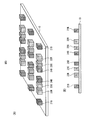
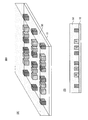
- FIG. 5A to FIG. 12B are diagrams showing manufacturing steps of the light emitting device 1.
- (A) of each figure shows the perspective view in each process
- (B) of each figure shows the longitudinal cross-sectional view of (A).
- the LED elements 21B, 22R, 23G, and 24B are mounted in one row in this order on the upper surface of the substrate 10 (step 1).
- step 1 an example in which six light emitting devices 1 are manufactured at the same time is shown, and a total of six sets of LED elements 21B, 22R, 23G, and 24B in three rows and two columns are mounted on the substrate 10.
- a plurality of sets of LED elements 21B, 22R, 23G, and 24B on the substrate 10 are formed with the sealing resin 50 by a method such as molding. It is coat
- the sealing resin 50 may be a simple transparent resin, but it is preferable to disperse and mix a scattering agent in the sealing resin 50.
- the sealing resin 50 obtained in step 2 is diced to form a groove 56 for the phosphor layer 30.
- Step 3 in order to make three light emitting devices 1 divided into two left and right rows of the substrate 10, two grooves 56 are formed.
- the phosphor layer 30 is formed by filling the groove 56 formed in step 3 with a resin containing a phosphor (step). 4).
- the four side surfaces of the sealing resin 50 scraped off in step 5, the inside of the groove 57, and the upper surface of the sealing resin 50 are reflective white.
- the resin frame 41 and the light shielding member 61 are formed by being covered with resin (step 6).
- resin it is preferable that the surface of the white resin is further covered with a black resin so that the resin frame 41 and the light shielding member 61 have a two-layer structure.
- FIGS. 11A and 11B dicing is performed on the portion where the groove 57 is formed (reference X) and the central portion of the substrate 10 orthogonal to the groove 57 (step 7). ). Thereby, as shown to FIG. 12 (A) and FIG. 12 (B), the six light-emitting devices 1 are completed. This completes the manufacturing process of the light emitting device 1.
- FIGS. 13 (A) to 13 (F) are top views of the light emitting devices 1, 1A, 1B, 1C, 1D, and 1E, respectively. In these drawings, a top view of the state in which the light shielding member 61 is removed is shown.
- the phosphor layer 30 may not be a wall-shaped member that bisects the sealing resin 50 between the LED element 21B and the LED element 22R.
- the phosphor layer fills the entire space surrounded by the three side walls of the resin frame 41 around the LED element 21B. Also good.
- the phosphor layer may have a square-shaped wall shape surrounding the LED element 21B.
- the resin frame may have an emission port 48C on the side with respect to the arrangement direction of the four LED elements.
- the emission port 48C is preferably provided only on the side of the LED elements 22R, 23G, and 24B. Light emitted from the light emitting device 1C is emitted from the emission port 48C in a direction parallel to the mounting surface of the substrate 10 and orthogonal to the arrangement direction of the four LED elements.
- the LED elements 22R, 23G, and 24B may be arranged in a triangular shape.
- the LED elements 24 ⁇ / b> R, 23 ⁇ / b> G, 24 ⁇ / b> B are farthest from the phosphor layer 30 in the region closer to the emission port 48 than the phosphor layer 30.
- it may be mounted in a triangular shape.
- the distance between the elements is shorter than when three LED elements are arranged on one straight line. For example, when three LED elements are arranged in a row transverse to the emission direction. Compared to, the color mixing property is improved.
- the LED element 22R may be disposed closer to the LED element 21B than the phosphor layer 30. Since red light does not excite the yellow phosphor in the phosphor layer 30, the position of the LED element 22R may be anywhere on the same mounting surface as the other LED elements 21B, 23G, and 24B.
- FIGS. 14A to 15B are views for explaining the structure of the light-emitting device 2.
- the light emitting device 2 includes a substrate 10, four LED elements 21B, 22R, 23G, and 24B, a phosphor layer 30, a resin frame 42, a sealing resin 50, and a light shielding member 62.
- the light emitting device 2 differs from the light emitting device 1 only in the shape of the resin frame and the light shielding member, and the light emitting direction, and has the same configuration as the light emitting device 1 in other points. Therefore, hereinafter, the light emitting device 2 will be described with respect to differences from the light emitting device 1, and the description overlapping with the light emitting device 1 will be omitted.
- the light emitting device 2 is a top-emitting LED package that can be used as an illumination light source or a light source for a backlight.
- FIG. 14A is a perspective view showing the light emitting device 1 to which the resin frame 42 and the light shielding member 62 are attached
- FIG. 14B is a longitudinal sectional view of FIG. 14A
- FIG. 14C is a perspective view showing the light emitting device 2 with the resin frame 42 and the light shielding member 62 removed
- FIG. 14D is a longitudinal sectional view of FIG. 14C
- FIG. 15A is a top view of the light emitting device 2 with the light shielding member 62 removed
- FIG. 15B is a longitudinal sectional view of FIG. 15A.
- the resin frame 42 is a resin member that surrounds the entire outer periphery of the substrate 10. Also in the light emitting device 2, as shown in FIG. 14B, the resin frame 42 includes an inner white resin layer 46 that reflects the emitted light from the LED elements 21B, 22R, 23G, and 24B to the sealing resin 50 side, It is preferable to have a two-layer structure with an outer black resin layer 47 that prevents the transmission of light to the outside.
- the presence of the white resin layer 46 improves color mixing, and the presence of the black resin layer 47 on the outside of the white resin layer 46 makes it difficult for light to leak to the outside, thereby improving the light emission efficiency.
- the light shielding member 62 is, for example, a resin sheet-like member, and is disposed about half of the upper surface of the sealing resin 50 so as to cover only the upper part of the LED element 21B.
- the light emitting device 2 has an emission port 49 above the LED elements 22R, 23G, and 24B. Light emitted from the LED elements 21B, 22R, 23G, and 24B is in a direction perpendicular to the mounting surface of the substrate 10 from the emission port 49. Is emitted.
- the light blocking member 62 includes an inner white sheet 66 that mainly reflects the emitted light from the LED element 21B to the sealing resin 50 side, and the light to the outside.
- the presence of the white sheet 66 improves the color mixing, and the presence of the black sheet 67 on the outside of the white sheet 66 makes it difficult for light to leak to the outside, thereby improving the light emission efficiency.
- 16 (A) to 16 (E) are top views of the light emitting devices 2, 2A, 2C, 2D, and 2E, respectively. In these drawings, a top view of the state where the light shielding member 62 is removed is shown.
- the phosphor layer 30 may not be a wall-shaped member that bisects the sealing resin 50 between the LED element 21B and the LED element 22R.
- the phosphor layer fills the entire space surrounded by the three side walls of the resin frame 42 around the LED element 21B. Also good.
- the phosphor layer may have a square-shaped wall shape surrounding the LED element 21B.
- the LED elements 22R, 23G, and 24B may be arranged in a triangular shape.
- the LED elements 22R, 23G, and 24B are replaced by the LED element 24B. It may be arranged in a triangular shape so as to be farthest from 30.
- the LED element 22R may be disposed closer to the LED element 21B than the phosphor layer 30. Since red light does not excite the yellow phosphor in the phosphor layer 30, the position of the LED element 22R may be anywhere on the same mounting surface as the other LED elements 21B, 23G, and 24B.
- FIGS. 17A to 17D are top views of other light emitting devices 1F, 1G, 2F, and 2G, respectively. These figures are longitudinal sectional views corresponding to FIG. 3B or FIG.
- the light emitting devices 1F, 1G, 2F, and 2G are different from the light emitting devices 1 and 2 only in the presence or absence of the scattering agent 55 in the sealing resin 50, and have the same configuration as the light emitting devices 1 and 2 in other points.
- the color mixing property is improved by dispersing and mixing the scattering agent 55 in the sealing resin 50, but the scattering agent 55 may be mixed uniformly in the entire sealing resin 50, or one of the sealing resins 50. You may mix only in a part. For example, as shown in FIGS.
- the scattering agent 55 may be mixed only in the sealing resin 50 on the LED element 21B side divided by the phosphor layer 30. As shown in FIG. 17B and FIG. 17D, the scattering agent 55 may be mixed only in the sealing resin 50 on the LED elements 22R, 23G, and 24B side.
- the side-emitting type light-emitting device 1 and the top-emitting type light-emitting device 2 for example, colorless and transparent containing a scattering agent only in the vicinity of the end face of the light-emitting surface where the exit ports 48 and 49 are located.
- a simple resin frame may be provided. Thus, even if the scattering agent is provided only in the vicinity of the end face of the light emitting surface, the color mixing property is improved.
- the corners of the resin frames 41 and 42 may be tapered or rounded.
- the luminous efficiency can be improved by such a shape change.
- the overall shape of the light emitting device may be changed as appropriate according to the application.
- FIG. 18A and FIG. 18B are diagrams for explaining the structure of the light-emitting device 3.
- 18A is a top view of the light-emitting device 3 corresponding to FIGS. 4A and 15A
- FIG. 18B is a longitudinal cross-sectional view of FIG. 18A.
- the light emitting device 3 includes a substrate 10, four LED elements 21B, 22R, 23G, and 24B, a phosphor layer 30, a resin frame 43, a sealing resin 50, and a light shielding member 61.
- the light emitting device 3 differs from the light emitting device 1 only in the shape of the resin frame and the light emitting direction, and has the same configuration as the light emitting device 1 in other points. For this reason, also about the light-emitting device 3, a different point from the light-emitting device 1 is demonstrated, and the description which overlaps with the light-emitting device 1 is abbreviate
- the resin frame 43 surrounds the outer periphery of the substrate 10 only in about half of the side on which the LED element 21B is mounted.
- the resin frame 43 is not provided on the substrate 10 in about half of the opposite side where the LED elements 22R, 23G, and 24B are mounted.
- the light shielding member 61 covers the entire upper surface of the sealing resin 50, as in the light emitting device 1. Therefore, in the light-emitting device 3, the regions 48L and 48R that are not covered by the resin frame 43 among the side surface 48 ′ that is forward in the LED element arrangement direction and the side surface that is lateral to the LED element arrangement direction are It becomes the exit.
- the light emitting device 3 emits light from these side surfaces 48 ′ and regions 48 ⁇ / b> L and 48 ⁇ / b> R in three directions as indicated by an arrow L in FIG.
- the light-emitting device 3 is a lateral three-surface-emitting LED package that can be used as an illumination light source or a light source for backlight.
- the light emission direction from the light emitting device is not limited to one direction of the side surface or the upper surface like the light emitting devices 1 and 2, and may be a plurality of directions like the light emitting device 3.
- one of the regions 48L and 48R may be covered with a resin frame so that light is emitted from the light emitting device in two directions, that is, the side surface 48 'and the region 48L or the region 48R.
- the LED elements 21B, 22R, 23G, and 24B in the resin frame 41 and 41C are arranged in front of the LED elements 22R.
- the resin frame 42 is disposed in front of the LED elements 21B, 22R, 23G, and 24B in the arrangement direction. It may be removed so that light can be emitted in two directions, side and upper.
- Each of the light emitting devices described above has LED elements 22R, 23G, and 24B that are red, green, and blue LED elements in the light emission path of the LED element 21B that emits white light. Thereby, in each light-emitting device, a color rendering property improves and it becomes possible to adjust the color of white light easily.
- the LED elements 23G and 24B are outside the phosphor layer 30, and in particular, the LED element 24B that can excite the phosphor is the phosphor layer. It is arranged at a position farthest from 30.
- the light emission of the LED elements 23G and 24B is not hindered by the phosphor, and the LED element 24B is difficult to excite the phosphor, so that even if the LED elements 21B and 24B emit light simultaneously.
- the excitation light is not generated unnecessarily.
- red, green, and blue LED elements are arranged in a row laterally with respect to the emission direction, color mixing may be deteriorated due to directivity.
- the LED elements 22R, 23G The color mixing property is improved by making the arrangement of 24B linear or triangular along the emission direction.
- the resin frames 41 to 43 and the light shielding members 61 and 62 are provided, light leaking from other than the exit ports 48 and 49 is reduced, so that the light emission efficiency is improved.
Landscapes
- Physics & Mathematics (AREA)
- General Physics & Mathematics (AREA)
- Optics & Photonics (AREA)
- Led Device Packages (AREA)
Abstract
Description
Claims (10)
- 蛍光体を含有する蛍光体層と、
前記蛍光体を励起して生成される蛍光との組合せにより白色光を出射する第1のLED素子と、
赤色光を出射する第2のLED素子と、
前記蛍光体層を挟んで前記第1のLED素子とは反対側に配置され、緑色光を出射する第3のLED素子と、
前記蛍光体層を挟んで前記第1のLED素子とは反対側で前記第2および第3のLED素子よりも前記蛍光体層から遠くに配置され、青色光を出射する第4のLED素子と、
前記第1から第4のLED素子が同じ実装面上に実装された基板と、
前記基板の外周の少なくとも一部を取り囲む樹脂枠と、
前記樹脂枠内の前記基板上に充填されて前記第1から第4のLED素子を封止する封止樹脂と、
前記実装面とは反対側の面である前記封止樹脂の上面に配置され、少なくとも前記第1のLED素子を覆う遮光部材と、
を有することを特徴とする発光装置。 - 前記封止樹脂には、光を拡散させる散乱剤が分散混入されている、請求項1に記載の発光装置。
- 前記樹脂枠は、前記封止樹脂の側に光を反射させる内側の白色樹脂層と、外部への光の透過を防止する外側の黒色樹脂層とを有する、請求項1または2に記載の発光装置。
- 前記遮光部材は、前記封止樹脂の側に光を反射させる内側の白色シートと、外部への光の透過を防止する外側の黒色シートとを有する、請求項1~3のいずれか一項に記載の発光装置。
- 前記遮光部材は、前記封止樹脂の上面全体を覆い、
前記樹脂枠は、前記第1から第4のLED素子による出射光の出射口を有し、
前記出射光は、前記出射口から前記実装面に平行な方向に出射される、請求項1~4のいずれか一項に記載の発光装置。 - 前記遮光部材は、前記第1のLED素子の上方を覆い、
前記樹脂枠は、前記基板の外周全体を取り囲み、
前記第1から第4のLED素子による出射光は、前記第2から第4のLED素子の上方から、前記実装面に垂直な方向に出射される、請求項1~4のいずれか一項に記載の発光装置。 - 前記第1から第4のLED素子は、前記実装面上において当該順序で1直線状に配列している、請求項1~6のいずれか一項に記載の発光装置。
- 前記蛍光体層は、前記第1のLED素子と前記第2のLED素子の間で前記封止樹脂を2分し、
前記第2のLED素子は、前記蛍光体層よりも前記第1のLED素子に近い側に配置されている、請求項7に記載の発光装置。 - 前記第2から第4のLED素子は、3角形状に配列している、請求項1~6のいずれか一項に記載の発光装置。
- 前記第3および第4のLED素子は、前記白色光および前記赤色光を透過させる透明な素子であり、
前記第2のLED素子は前記青色光を透過させない不透明な素子である、請求項1~9のいずれか一項に記載の発光装置。
Priority Applications (4)
| Application Number | Priority Date | Filing Date | Title |
|---|---|---|---|
| US15/760,785 US10707189B2 (en) | 2015-09-18 | 2016-09-20 | Light-emitting device |
| JP2017540048A JP6522139B2 (ja) | 2015-09-18 | 2016-09-20 | 発光装置 |
| CN201680048422.3A CN108028303B (zh) | 2015-09-18 | 2016-09-20 | 发光装置 |
| DE112016004229.9T DE112016004229B4 (de) | 2015-09-18 | 2016-09-20 | Licht emittierende Vorrichtung |
Applications Claiming Priority (2)
| Application Number | Priority Date | Filing Date | Title |
|---|---|---|---|
| JP2015185976 | 2015-09-18 | ||
| JP2015-185976 | 2015-09-18 |
Publications (1)
| Publication Number | Publication Date |
|---|---|
| WO2017047815A1 true WO2017047815A1 (ja) | 2017-03-23 |
Family
ID=58289537
Family Applications (1)
| Application Number | Title | Priority Date | Filing Date |
|---|---|---|---|
| PCT/JP2016/077736 Ceased WO2017047815A1 (ja) | 2015-09-18 | 2016-09-20 | 発光装置 |
Country Status (5)
| Country | Link |
|---|---|
| US (1) | US10707189B2 (ja) |
| JP (1) | JP6522139B2 (ja) |
| CN (1) | CN108028303B (ja) |
| DE (1) | DE112016004229B4 (ja) |
| WO (1) | WO2017047815A1 (ja) |
Cited By (2)
| Publication number | Priority date | Publication date | Assignee | Title |
|---|---|---|---|---|
| JP2019087600A (ja) * | 2017-11-06 | 2019-06-06 | シチズン電子株式会社 | 側面照射型led発光装置 |
| JP2025072651A (ja) * | 2020-03-09 | 2025-05-09 | エルジー イノテック カンパニー リミテッド | 照明モジュールおよびこれを備えた照明装置 |
Families Citing this family (8)
| Publication number | Priority date | Publication date | Assignee | Title |
|---|---|---|---|---|
| KR102358639B1 (ko) * | 2016-04-29 | 2022-02-07 | 루미리즈 홀딩 비.브이. | 고 휘도 크리스프 백색 led 광원 |
| KR102653015B1 (ko) * | 2018-07-18 | 2024-03-29 | 삼성전자주식회사 | 발광 장치, 운송 수단용 헤드램프, 및 그를 포함하는 운송 수단 |
| CN111463193B (zh) * | 2019-01-21 | 2021-11-12 | 光宝光电(常州)有限公司 | 芯片级发光二极管封装结构 |
| CN210624452U (zh) * | 2019-09-29 | 2020-05-26 | 漳州立达信光电子科技有限公司 | 一种led灯以及控制电路 |
| JP7196813B2 (ja) * | 2019-10-14 | 2022-12-27 | 豊田合成株式会社 | 発光装置およびその製造方法 |
| CN115735081B (zh) * | 2020-06-29 | 2025-12-16 | 西铁城电子株式会社 | 发光装置 |
| CN111785174A (zh) * | 2020-08-07 | 2020-10-16 | 京东方科技集团股份有限公司 | 柔性面板的支撑结构及其制作方法、柔性显示装置 |
| DE102024105959A1 (de) * | 2024-03-01 | 2025-09-04 | Ams-Osram International Gmbh | Optoelektronisches bauelement |
Citations (5)
| Publication number | Priority date | Publication date | Assignee | Title |
|---|---|---|---|---|
| JP2001024238A (ja) * | 1999-07-07 | 2001-01-26 | Citizen Electronics Co Ltd | 多色発光ダイオード |
| JP2004004626A (ja) * | 2002-03-27 | 2004-01-08 | Citizen Watch Co Ltd | 表示装置 |
| JP2006310613A (ja) * | 2005-04-28 | 2006-11-09 | Sharp Corp | 半導体発光装置 |
| JP2011192738A (ja) * | 2010-03-12 | 2011-09-29 | Seiwa Electric Mfg Co Ltd | 発光装置 |
| CN102593115A (zh) * | 2012-03-15 | 2012-07-18 | 深圳市丽晶光电科技股份有限公司 | Led表面贴装器件及其制造方法 |
Family Cites Families (12)
| Publication number | Priority date | Publication date | Assignee | Title |
|---|---|---|---|---|
| WO2000079605A1 (fr) | 1999-06-23 | 2000-12-28 | Citizen Electronics Co., Ltd. | Diode électroluminescente |
| JP4458804B2 (ja) | 2003-10-17 | 2010-04-28 | シチズン電子株式会社 | 白色led |
| JP4357311B2 (ja) | 2004-02-04 | 2009-11-04 | シチズン電子株式会社 | 発光ダイオードチップ |
| JP2008288412A (ja) | 2007-05-18 | 2008-11-27 | Citizen Electronics Co Ltd | Led発光装置 |
| JP2009246353A (ja) | 2008-03-10 | 2009-10-22 | Opt Link Co Ltd | Led低背光源装置及びled低背光源装置の製造方法 |
| CN101937911B (zh) | 2010-07-14 | 2013-07-24 | 深圳市华星光电技术有限公司 | 发光二极管封装构造及背光模块 |
| US20120014091A1 (en) | 2010-07-14 | 2012-01-19 | Shenzhen China Star Optoelectronics Technology Co Ltd. | Led package assembly and backlight module |
| WO2012046661A1 (ja) | 2010-10-07 | 2012-04-12 | シャープ株式会社 | 発光素子、発光装置、及び表示装置 |
| TW201513402A (zh) | 2013-09-27 | 2015-04-01 | Lextar Electronics Corp | 發光二極體封裝結構 |
| KR20150044307A (ko) | 2013-10-16 | 2015-04-24 | 주식회사 루멘스 | 측면 발광형 발광 소자 패키지와, 백라이트 유닛 및 측면 발광형 발광 소자 패키지의 제작 방법 |
| JP6230392B2 (ja) | 2013-11-29 | 2017-11-15 | シチズン電子株式会社 | 発光装置 |
| JP6269702B2 (ja) * | 2015-11-30 | 2018-01-31 | 日亜化学工業株式会社 | 発光装置の製造方法 |
-
2016
- 2016-09-20 US US15/760,785 patent/US10707189B2/en active Active
- 2016-09-20 JP JP2017540048A patent/JP6522139B2/ja not_active Expired - Fee Related
- 2016-09-20 DE DE112016004229.9T patent/DE112016004229B4/de not_active Expired - Fee Related
- 2016-09-20 CN CN201680048422.3A patent/CN108028303B/zh not_active Expired - Fee Related
- 2016-09-20 WO PCT/JP2016/077736 patent/WO2017047815A1/ja not_active Ceased
Patent Citations (5)
| Publication number | Priority date | Publication date | Assignee | Title |
|---|---|---|---|---|
| JP2001024238A (ja) * | 1999-07-07 | 2001-01-26 | Citizen Electronics Co Ltd | 多色発光ダイオード |
| JP2004004626A (ja) * | 2002-03-27 | 2004-01-08 | Citizen Watch Co Ltd | 表示装置 |
| JP2006310613A (ja) * | 2005-04-28 | 2006-11-09 | Sharp Corp | 半導体発光装置 |
| JP2011192738A (ja) * | 2010-03-12 | 2011-09-29 | Seiwa Electric Mfg Co Ltd | 発光装置 |
| CN102593115A (zh) * | 2012-03-15 | 2012-07-18 | 深圳市丽晶光电科技股份有限公司 | Led表面贴装器件及其制造方法 |
Cited By (4)
| Publication number | Priority date | Publication date | Assignee | Title |
|---|---|---|---|---|
| JP2019087600A (ja) * | 2017-11-06 | 2019-06-06 | シチズン電子株式会社 | 側面照射型led発光装置 |
| JP7072368B2 (ja) | 2017-11-06 | 2022-05-20 | シチズン電子株式会社 | 側面照射型led発光装置 |
| JP2025072651A (ja) * | 2020-03-09 | 2025-05-09 | エルジー イノテック カンパニー リミテッド | 照明モジュールおよびこれを備えた照明装置 |
| JP7846272B2 (ja) | 2020-03-09 | 2026-04-14 | エルジー イノテック カンパニー リミテッド | 照明モジュールおよびこれを備えた照明装置 |
Also Published As
| Publication number | Publication date |
|---|---|
| JP6522139B2 (ja) | 2019-05-29 |
| JPWO2017047815A1 (ja) | 2017-11-24 |
| DE112016004229T5 (de) | 2018-07-19 |
| CN108028303A (zh) | 2018-05-11 |
| US10707189B2 (en) | 2020-07-07 |
| US20180254263A1 (en) | 2018-09-06 |
| CN108028303B (zh) | 2020-01-24 |
| DE112016004229B4 (de) | 2022-08-25 |
Similar Documents
| Publication | Publication Date | Title |
|---|---|---|
| JP6522139B2 (ja) | 発光装置 | |
| JP5481587B2 (ja) | 発光素子 | |
| US9634203B2 (en) | Light emitting device, surface light source, liquid crystal display device, and method for manufacturing light emitting device | |
| CN100533795C (zh) | 发光装置 | |
| JP2015176960A (ja) | 発光装置 | |
| JP6282438B2 (ja) | 半導体発光装置 | |
| KR20220136961A (ko) | 백라이트 유닛 | |
| JP2016062899A (ja) | 半導体発光装置 | |
| US8641256B2 (en) | Semiconductor light emitting device, composite light emitting device with arrangement of semiconductor light emitting devices, and planar light source using composite light emitting device | |
| JP2023001231A (ja) | 発光装置 | |
| JP2008205170A (ja) | 発光半導体デバイス | |
| JP2019062058A (ja) | 発光装置 | |
| JP6266923B2 (ja) | Led発光装置 | |
| US20180190887A1 (en) | Light emitting device structure | |
| KR20170036295A (ko) | 반도체 발광소자 및 이의 제조방법 | |
| JP7285439B2 (ja) | 面状光源 | |
| JP7518374B2 (ja) | 発光装置 | |
| KR20170126423A (ko) | 반도체 발광소자 및 이의 제조방법 | |
| JP2024113533A (ja) | 発光装置 | |
| TW201523931A (zh) | 發光裝置 | |
| JP2002222996A (ja) | Led装置 | |
| JP2019186274A (ja) | 発光装置 | |
| KR20110094702A (ko) | 발광소자 패키지 |
Legal Events
| Date | Code | Title | Description |
|---|---|---|---|
| 121 | Ep: the epo has been informed by wipo that ep was designated in this application |
Ref document number: 16846686 Country of ref document: EP Kind code of ref document: A1 |
|
| ENP | Entry into the national phase |
Ref document number: 2017540048 Country of ref document: JP Kind code of ref document: A |
|
| WWE | Wipo information: entry into national phase |
Ref document number: 15760785 Country of ref document: US |
|
| WWE | Wipo information: entry into national phase |
Ref document number: 112016004229 Country of ref document: DE |
|
| 122 | Ep: pct application non-entry in european phase |
Ref document number: 16846686 Country of ref document: EP Kind code of ref document: A1 |