WO2017013904A1 - メタルマスク基材、メタルマスク基材の管理方法、メタルマスク、および、メタルマスクの製造方法 - Google Patents
メタルマスク基材、メタルマスク基材の管理方法、メタルマスク、および、メタルマスクの製造方法 Download PDFInfo
- Publication number
- WO2017013904A1 WO2017013904A1 PCT/JP2016/059042 JP2016059042W WO2017013904A1 WO 2017013904 A1 WO2017013904 A1 WO 2017013904A1 JP 2016059042 W JP2016059042 W JP 2016059042W WO 2017013904 A1 WO2017013904 A1 WO 2017013904A1
- Authority
- WO
- WIPO (PCT)
- Prior art keywords
- metal mask
- reflectance
- base material
- metal
- resist
- Prior art date
- Legal status (The legal status is an assumption and is not a legal conclusion. Google has not performed a legal analysis and makes no representation as to the accuracy of the status listed.)
- Ceased
Links
Images









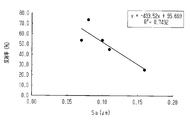

Classifications
-
- C—CHEMISTRY; METALLURGY
- C23—COATING METALLIC MATERIAL; COATING MATERIAL WITH METALLIC MATERIAL; CHEMICAL SURFACE TREATMENT; DIFFUSION TREATMENT OF METALLIC MATERIAL; COATING BY VACUUM EVAPORATION, BY SPUTTERING, BY ION IMPLANTATION OR BY CHEMICAL VAPOUR DEPOSITION, IN GENERAL; INHIBITING CORROSION OF METALLIC MATERIAL OR INCRUSTATION IN GENERAL
- C23C—COATING METALLIC MATERIAL; COATING MATERIAL WITH METALLIC MATERIAL; SURFACE TREATMENT OF METALLIC MATERIAL BY DIFFUSION INTO THE SURFACE, BY CHEMICAL CONVERSION OR SUBSTITUTION; COATING BY VACUUM EVAPORATION, BY SPUTTERING, BY ION IMPLANTATION OR BY CHEMICAL VAPOUR DEPOSITION, IN GENERAL
- C23C14/00—Coating by vacuum evaporation, by sputtering or by ion implantation of the coating forming material
- C23C14/04—Coating on selected surface areas, e.g. using masks
- C23C14/042—Coating on selected surface areas, e.g. using masks using masks
-
- C—CHEMISTRY; METALLURGY
- C23—COATING METALLIC MATERIAL; COATING MATERIAL WITH METALLIC MATERIAL; CHEMICAL SURFACE TREATMENT; DIFFUSION TREATMENT OF METALLIC MATERIAL; COATING BY VACUUM EVAPORATION, BY SPUTTERING, BY ION IMPLANTATION OR BY CHEMICAL VAPOUR DEPOSITION, IN GENERAL; INHIBITING CORROSION OF METALLIC MATERIAL OR INCRUSTATION IN GENERAL
- C23C—COATING METALLIC MATERIAL; COATING MATERIAL WITH METALLIC MATERIAL; SURFACE TREATMENT OF METALLIC MATERIAL BY DIFFUSION INTO THE SURFACE, BY CHEMICAL CONVERSION OR SUBSTITUTION; COATING BY VACUUM EVAPORATION, BY SPUTTERING, BY ION IMPLANTATION OR BY CHEMICAL VAPOUR DEPOSITION, IN GENERAL
- C23C14/00—Coating by vacuum evaporation, by sputtering or by ion implantation of the coating forming material
- C23C14/02—Pretreatment of the material to be coated
- C23C14/024—Deposition of sublayers, e.g. to promote adhesion of the coating
-
- C—CHEMISTRY; METALLURGY
- C23—COATING METALLIC MATERIAL; COATING MATERIAL WITH METALLIC MATERIAL; CHEMICAL SURFACE TREATMENT; DIFFUSION TREATMENT OF METALLIC MATERIAL; COATING BY VACUUM EVAPORATION, BY SPUTTERING, BY ION IMPLANTATION OR BY CHEMICAL VAPOUR DEPOSITION, IN GENERAL; INHIBITING CORROSION OF METALLIC MATERIAL OR INCRUSTATION IN GENERAL
- C23C—COATING METALLIC MATERIAL; COATING MATERIAL WITH METALLIC MATERIAL; SURFACE TREATMENT OF METALLIC MATERIAL BY DIFFUSION INTO THE SURFACE, BY CHEMICAL CONVERSION OR SUBSTITUTION; COATING BY VACUUM EVAPORATION, BY SPUTTERING, BY ION IMPLANTATION OR BY CHEMICAL VAPOUR DEPOSITION, IN GENERAL
- C23C14/00—Coating by vacuum evaporation, by sputtering or by ion implantation of the coating forming material
- C23C14/02—Pretreatment of the material to be coated
- C23C14/028—Physical treatment to alter the texture of the substrate surface, e.g. grinding, polishing
-
- C—CHEMISTRY; METALLURGY
- C23—COATING METALLIC MATERIAL; COATING MATERIAL WITH METALLIC MATERIAL; CHEMICAL SURFACE TREATMENT; DIFFUSION TREATMENT OF METALLIC MATERIAL; COATING BY VACUUM EVAPORATION, BY SPUTTERING, BY ION IMPLANTATION OR BY CHEMICAL VAPOUR DEPOSITION, IN GENERAL; INHIBITING CORROSION OF METALLIC MATERIAL OR INCRUSTATION IN GENERAL
- C23C—COATING METALLIC MATERIAL; COATING MATERIAL WITH METALLIC MATERIAL; SURFACE TREATMENT OF METALLIC MATERIAL BY DIFFUSION INTO THE SURFACE, BY CHEMICAL CONVERSION OR SUBSTITUTION; COATING BY VACUUM EVAPORATION, BY SPUTTERING, BY ION IMPLANTATION OR BY CHEMICAL VAPOUR DEPOSITION, IN GENERAL
- C23C14/00—Coating by vacuum evaporation, by sputtering or by ion implantation of the coating forming material
- C23C14/04—Coating on selected surface areas, e.g. using masks
-
- C—CHEMISTRY; METALLURGY
- C23—COATING METALLIC MATERIAL; COATING MATERIAL WITH METALLIC MATERIAL; CHEMICAL SURFACE TREATMENT; DIFFUSION TREATMENT OF METALLIC MATERIAL; COATING BY VACUUM EVAPORATION, BY SPUTTERING, BY ION IMPLANTATION OR BY CHEMICAL VAPOUR DEPOSITION, IN GENERAL; INHIBITING CORROSION OF METALLIC MATERIAL OR INCRUSTATION IN GENERAL
- C23C—COATING METALLIC MATERIAL; COATING MATERIAL WITH METALLIC MATERIAL; SURFACE TREATMENT OF METALLIC MATERIAL BY DIFFUSION INTO THE SURFACE, BY CHEMICAL CONVERSION OR SUBSTITUTION; COATING BY VACUUM EVAPORATION, BY SPUTTERING, BY ION IMPLANTATION OR BY CHEMICAL VAPOUR DEPOSITION, IN GENERAL
- C23C14/00—Coating by vacuum evaporation, by sputtering or by ion implantation of the coating forming material
- C23C14/06—Coating by vacuum evaporation, by sputtering or by ion implantation of the coating forming material characterised by the coating material
- C23C14/08—Oxides
- C23C14/085—Oxides of iron group metals
-
- C—CHEMISTRY; METALLURGY
- C23—COATING METALLIC MATERIAL; COATING MATERIAL WITH METALLIC MATERIAL; CHEMICAL SURFACE TREATMENT; DIFFUSION TREATMENT OF METALLIC MATERIAL; COATING BY VACUUM EVAPORATION, BY SPUTTERING, BY ION IMPLANTATION OR BY CHEMICAL VAPOUR DEPOSITION, IN GENERAL; INHIBITING CORROSION OF METALLIC MATERIAL OR INCRUSTATION IN GENERAL
- C23C—COATING METALLIC MATERIAL; COATING MATERIAL WITH METALLIC MATERIAL; SURFACE TREATMENT OF METALLIC MATERIAL BY DIFFUSION INTO THE SURFACE, BY CHEMICAL CONVERSION OR SUBSTITUTION; COATING BY VACUUM EVAPORATION, BY SPUTTERING, BY ION IMPLANTATION OR BY CHEMICAL VAPOUR DEPOSITION, IN GENERAL
- C23C14/00—Coating by vacuum evaporation, by sputtering or by ion implantation of the coating forming material
- C23C14/06—Coating by vacuum evaporation, by sputtering or by ion implantation of the coating forming material characterised by the coating material
- C23C14/12—Organic material
-
- C—CHEMISTRY; METALLURGY
- C23—COATING METALLIC MATERIAL; COATING MATERIAL WITH METALLIC MATERIAL; CHEMICAL SURFACE TREATMENT; DIFFUSION TREATMENT OF METALLIC MATERIAL; COATING BY VACUUM EVAPORATION, BY SPUTTERING, BY ION IMPLANTATION OR BY CHEMICAL VAPOUR DEPOSITION, IN GENERAL; INHIBITING CORROSION OF METALLIC MATERIAL OR INCRUSTATION IN GENERAL
- C23C—COATING METALLIC MATERIAL; COATING MATERIAL WITH METALLIC MATERIAL; SURFACE TREATMENT OF METALLIC MATERIAL BY DIFFUSION INTO THE SURFACE, BY CHEMICAL CONVERSION OR SUBSTITUTION; COATING BY VACUUM EVAPORATION, BY SPUTTERING, BY ION IMPLANTATION OR BY CHEMICAL VAPOUR DEPOSITION, IN GENERAL
- C23C14/00—Coating by vacuum evaporation, by sputtering or by ion implantation of the coating forming material
- C23C14/22—Coating by vacuum evaporation, by sputtering or by ion implantation of the coating forming material characterised by the process of coating
- C23C14/225—Oblique incidence of vaporised material on substrate
-
- C—CHEMISTRY; METALLURGY
- C23—COATING METALLIC MATERIAL; COATING MATERIAL WITH METALLIC MATERIAL; CHEMICAL SURFACE TREATMENT; DIFFUSION TREATMENT OF METALLIC MATERIAL; COATING BY VACUUM EVAPORATION, BY SPUTTERING, BY ION IMPLANTATION OR BY CHEMICAL VAPOUR DEPOSITION, IN GENERAL; INHIBITING CORROSION OF METALLIC MATERIAL OR INCRUSTATION IN GENERAL
- C23C—COATING METALLIC MATERIAL; COATING MATERIAL WITH METALLIC MATERIAL; SURFACE TREATMENT OF METALLIC MATERIAL BY DIFFUSION INTO THE SURFACE, BY CHEMICAL CONVERSION OR SUBSTITUTION; COATING BY VACUUM EVAPORATION, BY SPUTTERING, BY ION IMPLANTATION OR BY CHEMICAL VAPOUR DEPOSITION, IN GENERAL
- C23C14/00—Coating by vacuum evaporation, by sputtering or by ion implantation of the coating forming material
- C23C14/22—Coating by vacuum evaporation, by sputtering or by ion implantation of the coating forming material characterised by the process of coating
- C23C14/24—Vacuum evaporation
-
- C—CHEMISTRY; METALLURGY
- C23—COATING METALLIC MATERIAL; COATING MATERIAL WITH METALLIC MATERIAL; CHEMICAL SURFACE TREATMENT; DIFFUSION TREATMENT OF METALLIC MATERIAL; COATING BY VACUUM EVAPORATION, BY SPUTTERING, BY ION IMPLANTATION OR BY CHEMICAL VAPOUR DEPOSITION, IN GENERAL; INHIBITING CORROSION OF METALLIC MATERIAL OR INCRUSTATION IN GENERAL
- C23F—NON-MECHANICAL REMOVAL OF METALLIC MATERIAL FROM SURFACE; INHIBITING CORROSION OF METALLIC MATERIAL OR INCRUSTATION IN GENERAL; MULTI-STEP PROCESSES FOR SURFACE TREATMENT OF METALLIC MATERIAL INVOLVING AT LEAST ONE PROCESS PROVIDED FOR IN CLASS C23 AND AT LEAST ONE PROCESS COVERED BY SUBCLASS C21D OR C22F OR CLASS C25
- C23F1/00—Etching metallic material by chemical means
- C23F1/02—Local etching
-
- C—CHEMISTRY; METALLURGY
- C23—COATING METALLIC MATERIAL; COATING MATERIAL WITH METALLIC MATERIAL; CHEMICAL SURFACE TREATMENT; DIFFUSION TREATMENT OF METALLIC MATERIAL; COATING BY VACUUM EVAPORATION, BY SPUTTERING, BY ION IMPLANTATION OR BY CHEMICAL VAPOUR DEPOSITION, IN GENERAL; INHIBITING CORROSION OF METALLIC MATERIAL OR INCRUSTATION IN GENERAL
- C23F—NON-MECHANICAL REMOVAL OF METALLIC MATERIAL FROM SURFACE; INHIBITING CORROSION OF METALLIC MATERIAL OR INCRUSTATION IN GENERAL; MULTI-STEP PROCESSES FOR SURFACE TREATMENT OF METALLIC MATERIAL INVOLVING AT LEAST ONE PROCESS PROVIDED FOR IN CLASS C23 AND AT LEAST ONE PROCESS COVERED BY SUBCLASS C21D OR C22F OR CLASS C25
- C23F1/00—Etching metallic material by chemical means
- C23F1/10—Etching compositions
- C23F1/14—Aqueous compositions
-
- C—CHEMISTRY; METALLURGY
- C23—COATING METALLIC MATERIAL; COATING MATERIAL WITH METALLIC MATERIAL; CHEMICAL SURFACE TREATMENT; DIFFUSION TREATMENT OF METALLIC MATERIAL; COATING BY VACUUM EVAPORATION, BY SPUTTERING, BY ION IMPLANTATION OR BY CHEMICAL VAPOUR DEPOSITION, IN GENERAL; INHIBITING CORROSION OF METALLIC MATERIAL OR INCRUSTATION IN GENERAL
- C23F—NON-MECHANICAL REMOVAL OF METALLIC MATERIAL FROM SURFACE; INHIBITING CORROSION OF METALLIC MATERIAL OR INCRUSTATION IN GENERAL; MULTI-STEP PROCESSES FOR SURFACE TREATMENT OF METALLIC MATERIAL INVOLVING AT LEAST ONE PROCESS PROVIDED FOR IN CLASS C23 AND AT LEAST ONE PROCESS COVERED BY SUBCLASS C21D OR C22F OR CLASS C25
- C23F1/00—Etching metallic material by chemical means
- C23F1/44—Compositions for etching metallic material from a metallic material substrate of different composition
-
- G—PHYSICS
- G01—MEASURING; TESTING
- G01N—INVESTIGATING OR ANALYSING MATERIALS BY DETERMINING THEIR CHEMICAL OR PHYSICAL PROPERTIES
- G01N21/00—Investigating or analysing materials by the use of optical means, i.e. using sub-millimetre waves, infrared, visible or ultraviolet light
- G01N21/17—Systems in which incident light is modified in accordance with the properties of the material investigated
- G01N21/55—Specular reflectivity
-
- G—PHYSICS
- G03—PHOTOGRAPHY; CINEMATOGRAPHY; ANALOGOUS TECHNIQUES USING WAVES OTHER THAN OPTICAL WAVES; ELECTROGRAPHY; HOLOGRAPHY
- G03F—PHOTOMECHANICAL PRODUCTION OF TEXTURED OR PATTERNED SURFACES, e.g. FOR PRINTING, FOR PROCESSING OF SEMICONDUCTOR DEVICES; MATERIALS THEREFOR; ORIGINALS THEREFOR; APPARATUS SPECIALLY ADAPTED THEREFOR
- G03F7/00—Photomechanical, e.g. photolithographic, production of textured or patterned surfaces, e.g. printing surfaces; Materials therefor, e.g. comprising photoresists; Apparatus specially adapted therefor
- G03F7/0002—Lithographic processes using patterning methods other than those involving the exposure to radiation, e.g. by stamping
-
- H—ELECTRICITY
- H10—SEMICONDUCTOR DEVICES; ELECTRIC SOLID-STATE DEVICES NOT OTHERWISE PROVIDED FOR
- H10K—ORGANIC ELECTRIC SOLID-STATE DEVICES
- H10K50/00—Organic light-emitting devices
- H10K50/10—OLEDs or polymer light-emitting diodes [PLED]
- H10K50/11—OLEDs or polymer light-emitting diodes [PLED] characterised by the electroluminescent [EL] layers
-
- H—ELECTRICITY
- H10—SEMICONDUCTOR DEVICES; ELECTRIC SOLID-STATE DEVICES NOT OTHERWISE PROVIDED FOR
- H10K—ORGANIC ELECTRIC SOLID-STATE DEVICES
- H10K50/00—Organic light-emitting devices
- H10K50/80—Constructional details
- H10K50/85—Arrangements for extracting light from the devices
- H10K50/856—Arrangements for extracting light from the devices comprising reflective means
-
- H—ELECTRICITY
- H10—SEMICONDUCTOR DEVICES; ELECTRIC SOLID-STATE DEVICES NOT OTHERWISE PROVIDED FOR
- H10K—ORGANIC ELECTRIC SOLID-STATE DEVICES
- H10K71/00—Manufacture or treatment specially adapted for the organic devices covered by this subclass
-
- H—ELECTRICITY
- H10—SEMICONDUCTOR DEVICES; ELECTRIC SOLID-STATE DEVICES NOT OTHERWISE PROVIDED FOR
- H10K—ORGANIC ELECTRIC SOLID-STATE DEVICES
- H10K71/00—Manufacture or treatment specially adapted for the organic devices covered by this subclass
- H10K71/10—Deposition of organic active material
- H10K71/16—Deposition of organic active material using physical vapour deposition [PVD], e.g. vacuum deposition or sputtering
- H10K71/166—Deposition of organic active material using physical vapour deposition [PVD], e.g. vacuum deposition or sputtering using selective deposition, e.g. using a mask
-
- H—ELECTRICITY
- H10—SEMICONDUCTOR DEVICES; ELECTRIC SOLID-STATE DEVICES NOT OTHERWISE PROVIDED FOR
- H10K—ORGANIC ELECTRIC SOLID-STATE DEVICES
- H10K71/00—Manufacture or treatment specially adapted for the organic devices covered by this subclass
- H10K71/20—Changing the shape of the active layer in the devices, e.g. patterning
- H10K71/231—Changing the shape of the active layer in the devices, e.g. patterning by etching of existing layers
- H10K71/233—Changing the shape of the active layer in the devices, e.g. patterning by etching of existing layers by photolithographic etching
-
- H—ELECTRICITY
- H10—SEMICONDUCTOR DEVICES; ELECTRIC SOLID-STATE DEVICES NOT OTHERWISE PROVIDED FOR
- H10P—GENERIC PROCESSES OR APPARATUS FOR THE MANUFACTURE OR TREATMENT OF DEVICES COVERED BY CLASS H10
- H10P76/00—Manufacture or treatment of masks on semiconductor bodies, e.g. by lithography or photolithography
- H10P76/40—Manufacture or treatment of masks on semiconductor bodies, e.g. by lithography or photolithography of masks comprising inorganic materials
- H10P76/408—Manufacture or treatment of masks on semiconductor bodies, e.g. by lithography or photolithography of masks comprising inorganic materials characterised by their sizes, orientations, dispositions, behaviours or shapes
- H10P76/4085—Manufacture or treatment of masks on semiconductor bodies, e.g. by lithography or photolithography of masks comprising inorganic materials characterised by their sizes, orientations, dispositions, behaviours or shapes characterised by the processes involved to create the masks
Definitions
- the present invention is a metal mask base material having a metal surface on which a resist is arranged, for example, a metal mask base material for forming a metal mask for an organic EL element, and a method for managing the metal mask base material
- the present invention relates to a metal mask and a metal mask manufacturing method.
- a metal mask substrate which is a metal plate is used.
- a coating liquid containing a resist layer forming material is applied to the application surface of the metal mask base material, whereby a resist layer is formed.
- the resist layer is exposed and developed to form a resist layer having a predetermined pattern, and the metal mask base material is etched through the resist layer, whereby a metal mask is manufactured.
- the thickness of the resist layer varies depending on the amount of coating liquid applied to the coating surface and the degree to which the coating liquid is dried. May vary.
- a dry film resist as the resist layer (see, for example, Patent Document 1).
- the resist layer formed using the coating liquid is a layer in which the coating liquid directly applied to the metal mask substrate is cured on the coating surface, so that it is easy to form a shape following the coating surface. Therefore, it is easy to adhere to the metal mask base material.
- the resist layer formed from the dry film resist is formed by a coating liquid because a layer that is a separate body from the metal mask base material is affixed to one surface of the metal mask base material. Compared to the resist layer, it has a shape that hardly follows the coated surface, and therefore, a part of the resist layer may be peeled off from the metal mask substrate.
- the surface in contact with the resist layer is not limited to a metal mask substrate formed of a metal plate, for example, a laminate of a resin layer and a metal layer or a laminate in which a resin layer is sandwiched between metal layers.
- a metal mask substrate formed of a metal plate
- the metal mask base material is made of metal or alloy.
- the above-described circumstances are common in a resist layer having low adhesion to a metal mask substrate.
- the present invention provides a metal mask substrate having a surface capable of enhancing adhesion at the interface between the resist and the surface, a method for managing the metal mask substrate, a metal mask, and a method for manufacturing the metal mask. Objective.
- a metal mask base material for solving the above-mentioned problems comprises a metal surface configured to be arranged with a resist, and the reflectance in regular reflection of light incident on the surface is 45.2% or more. is there.
- the management method of the metal mask base material for solving the said subject prepares a metal mask base material provided with the metal surface comprised so that a resist may be arrange
- the reflectance in regular reflection is 45.2% or more, it has been found that the surface roughness is reduced to such an extent that adhesion at the interface between the resist and the surface is enhanced, so that the resist is hardly peeled off from the surface. .
- the reflectance at regular reflection is 45.2% or more for the light incident on the surface, so that the adhesion at the interface between the surface of the metal mask substrate and the resist is improved. Can do.
- a direction orthogonal to the rolling direction of the metal mask base material is a width direction, and is a first plane perpendicular to the surface, and is within the first plane orthogonal to the rolling direction.
- the reflectance in the regular reflection is the first reflectance
- the reflectance in the regular reflection in the second plane perpendicular to the width direction is the second reflectance. It is.
- the second reflectance may be greater than the first reflectance, and the first reflectance may be 45.2% or more.
- the adhesion at the interface between the surface of the metal mask base material and the resist is further improved. Can be increased.
- the surface may include a portion in which a difference obtained by subtracting the first reflectance from the second reflectance is 10.2% or more.
- the above configuration is more preferable for improving the adhesion at the interface between the surface of the metal mask substrate and the resist because the surface includes a portion where the second reflectance is 10.2% or more larger than the first reflectance. .
- the surface may have a three-dimensional surface roughness Sa of 0.11 ⁇ m or less and a three-dimensional surface roughness Sz of 3.17 ⁇ m or less.
- the reflectance in regular reflection is 45.2% or more, and the three-dimensional surface roughness Sa is 0.11 ⁇ m or less. Since the thickness Sz is 3.17 ⁇ m or less, the adhesion at the interface between the resist and the surface is more reliably increased.
- the surface is a first surface
- the resist is a first resist
- a second resist is arranged.
- the metal second surface may be further provided, and the reflectance in the regular reflection of the light incident on the second surface may be 45.2% or more.
- the adhesion between the first surface and the first resist and the adhesion between the second surface and the second resist are improved. Therefore, in the etching on the first surface and the second surface, processing is performed. It is possible to improve the accuracy.
- the surface may be made of Invar. According to the above configuration, since the linear expansion coefficient of the glass substrate and the linear expansion coefficient of Invar are approximately the same, the metal mask formed from the metal mask base material is applied to film formation on the glass substrate, that is, the shape It is possible to apply a metal mask with improved accuracy to film formation on a glass substrate.
- the resist is preferably a dry film resist, and the surface is preferably configured such that the dry film resist is attached.
- the resist is a dry film resist and the surface is configured to be attached with the dry film resist.
- the adhesion between the metal surface configured to be attached with the dry film resist and the dry film resist is enhanced.
- a metal mask for solving the above-described problems is a metal mask provided with a metal mask base having a metal surface.
- the metal mask base includes a plurality of through holes having openings on the surface while penetrating the metal mask base along the thickness direction of the metal mask base.
- a method of manufacturing a metal mask for solving the above-described problem includes a metal surface configured so that a resist is disposed, and the three-dimensional surface roughness Sa of the surface is 0.11 ⁇ m or less, and the surface Preparing a metal mask base material having a three-dimensional surface roughness Sz of 3.17 ⁇ m or less, disposing a resist on the surface, and in the thickness direction of the metal mask base material on the metal mask base material Forming a plurality of recesses in the metal mask base material through the resist, and forming through holes for forming a plurality of recesses having depressions along the surface and having openings on the surface. And comprising.
- an average value in the dimension of the opening in a plan view facing the surface is A, and a value obtained by multiplying the standard deviation of the dimension by 3 is B.
- the said recessed part is formed in the said several metal mask base material so that (B / A) * 100 (%) may be 10% or less.
- the adhesion at the interface between the resist and the surface can be enhanced in the metal mask base material.
- the management method of the metal mask base material by which the adhesiveness in the interface of a resist and the surface was improved can be provided.
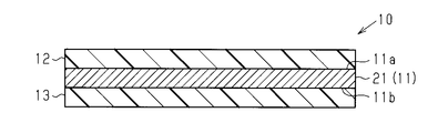
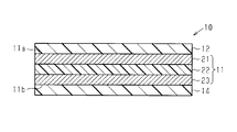
- FIG. 1 It is a fragmentary perspective view which shows the partial perspective structure of the metal mask base material for dry film resist in one Embodiment which actualized the metal mask base material of this invention as a metal mask base material for dry film resist. It is a fragmentary sectional view which shows the partial cross-section in an example of the metal mask base material for dry film resists. It is a fragmentary sectional view which shows the partial cross-section in an example of the metal mask base material for dry film resists. It is a fragmentary sectional view which shows the partial cross-section in an example of the metal mask base material for dry film resists.
- FIG. 1 shows the partial perspective structure of the metal mask base material for dry film resist in one Embodiment which actualized the metal mask base material of this invention as a metal mask base material for dry film resist. It is a fragmentary sectional view which shows the partial cross-section in an example of the metal mask base material for dry film resists. It is a fragmentary sectional view which shows the partial cross-section in an example of the metal mask base material
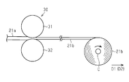
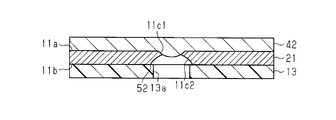
- FIG. 5 is a process diagram for explaining a method for managing a metal mask substrate for dry film resist in one embodiment in which the method for managing a metal mask substrate of the present invention is embodied as a method for managing a metal mask substrate for dry film resist. is there. It is process drawing for demonstrating the manufacturing method of the metal mask base material for dry film resists, Comprising: It is process drawing which shows the process of rolling the base material formed from the invar. It is process drawing for demonstrating the manufacturing method of the metal mask base material for dry film resists, Comprising: It is process drawing which shows the process of annealing a rolling material. It is process drawing for demonstrating the manufacturing method of a metal mask, Comprising: It is process drawing which shows the process of sticking a dry film resist.
- the metal mask base material and the metal mask base material management method of the present invention are embodied as a dry film resist metal mask and a dry film resist metal mask management method.
- a dry film resist metal mask and a dry film resist metal mask management method One embodiment of the metal mask and the method of manufacturing the metal mask will be described.
- the metal mask manufactured using the metal mask base material for dry film resist in this embodiment is used when the organic material which comprises an organic EL element is vapor-deposited with respect to a glass substrate in the manufacturing process of an organic EL element. It is a mask.
- the metal mask base material 11 is an example of a metal mask base material for dry film resist, and is a metal layer that spreads along one surface.
- the metal mask base material 11 is provided with the metal 1st surface 11a, and the 1st surface 11a is an example of the surface comprised so that a resist may be arrange
- the reflectance in the regular reflection of the light which injected into the 1st surface 11a is 45.2% or more.
- the reflectance in regular reflection is light emitted from a halogen lamp and incident light having an incident angle of 45 ° ⁇ 0.2 ° with respect to the normal direction of the first surface 11a of the metal mask base 11. It is the reflectance in regular reflection.
- the first surface 11a of the metal mask base material 11 is attached to the surface.
- the adhesion at the interface with the first dry film resist 12 which is an example of the attached dry film resist can be improved.
- the laminated body in which the first dry film resist 12 is attached to the first surface 11a of the metal mask base material 11 is a metal mask forming intermediate 10 that is an intermediate for forming a metal mask.
- the direction rolled when the metal mask base material 11 is manufactured is a rolling direction
- the direction orthogonal to the rolling direction is the width direction.
- the reflectance on the first surface 11a of the metal mask substrate 11 the reflectance in the regular reflection in the first plane perpendicular to the first surface 11a and perpendicular to the rolling direction is the first reflection. Rate.
- the reflectance in the regular reflection in the second plane perpendicular to the first surface 11a and orthogonal to the width direction is the second reflectance.
- the second reflectance is larger than the first reflectance, and the first reflectance is 45.2% or more.
- the relatively small reflectivity is 45.2% or more, so the adhesion at the interface between the surface of the metal mask substrate 11 and the dry film resist 12 is improved. Can be increased.
- the first surface 11a includes a portion where the difference obtained by subtracting the first reflectance from the second reflectance is 10.2% or more. Since the first surface 11a includes a portion where the second reflectance is 10.2% or more larger than the first reflectance, the adhesion at the interface between the first surface 11a of the metal mask base material 11 and the dry film resist 12 is increased. It is more preferable to increase the value.
- the three-dimensional surface roughness Sa is 0.11 ⁇ m or less, and the three-dimensional surface roughness Sz is 3.17 ⁇ m or less.
- the three-dimensional surface roughness Sa and the three-dimensional surface roughness Sz are values measured by a method according to ISO 25178.
- the three-dimensional surface roughness Sa is the arithmetic average height Sa in the definition region having a predetermined area, and the three-dimensional surface roughness Sz is the maximum height Sz in the definition region having a predetermined area.
- the three-dimensional surface roughness Sa is 0.11 ⁇ m or less and the three-dimensional surface roughness Sz is 3 while the reflectance in regular reflection is 45.2% or more. Since the thickness is 17 ⁇ m or less, the adhesion at the interface between the first dry film resist 12 and the first surface 11a is more reliably increased.
- the material for forming the metal layer is, for example, invar, that is, an alloy containing iron and nickel as main components, and is preferably an alloy containing 36% by mass of nickel.
- the surface of the metal mask base material 11 is preferably made of Invar.
- the linear expansion coefficient of Invar is about 1.2 ⁇ 10 ⁇ 6 / ° C.
- the thickness of the metal layer is preferably 10 ⁇ m or more and 50 ⁇ m or less, for example.
- the material for forming the metal layer is Invar
- the linear expansion coefficient of the glass substrate and the linear expansion coefficient of Invar are approximately the same, so the metal mask formed from the metal mask base material 11 is applied to film formation on the glass substrate. In other words, it is possible to apply a metal mask whose shape accuracy is improved to film formation on a glass substrate.
- the first dry film resist 12 is formed of, for example, a negative resist that is an example of a photosensitive material.
- the material for forming the first dry film resist 12 is, for example, an acrylic resin that is crosslinked by photopolymerization.
- the thickness of the first dry film resist 12 is preferably 5 ⁇ m or more and 20 ⁇ m or less, for example.
- the first dry film resist 12 may be formed from a positive resist, but in general, a negative resist is often used as a material for forming the first dry film resist 12.
- FIG. 2 shows a first embodiment in which the metal mask base material 11 is composed of one metal layer
- FIG. 3 shows that the metal mask base material 11 has one metal layer and one resin layer.
- the 2nd form which is an example comprised from is shown.
- FIG. 4 has shown the 3rd form which is an example in which the metal mask base material 11 is comprised from two metal layers and one resin layer.
- the metal layer 21 includes a second surface 11b that is a surface opposite to the first surface 11a.
- the first surface 11a is a metal surface configured such that the first dry film resist 12 is attached thereto
- the second surface 11b is a metal surface configured such that the resist is disposed. Is a metal surface configured such that the second dry film resist 13 is attached thereto.
- the metal mask forming intermediate 10 includes a metal layer 21, a first dry film resist 12, and a second dry film resist 13.
- the reflectance in regular reflection is 45.2% or more.
- the adhesion between the second dry film resist 13 and the metal layer 21 can be enhanced also on the second surface 11 b.
- the second surface 11b it is preferable that the three-dimensional surface roughness Sa is 0.11 ⁇ m or less and the three-dimensional surface roughness Sz is 3.17 ⁇ m or less, like the first surface 11a.
- the second surface 11b in addition to the first surface 11a, also has more adhesion at the interface between the second dry film resist 13 and the second surface 11b. Will definitely increase.
- the material for forming the second dry film resist 13 is an acrylic resin that is cross-linked by, for example, photopolymerization, like the first dry film resist 12.
- the thickness of the 2nd dry film resist 13 is 5 micrometers or more and 20 micrometers or less, for example.
- the metal mask base material 11 may include a metal layer 21 and a resin layer 22 located on the opposite side of the metal layer 21 from the first dry film resist 12. It is preferable that the linear expansion coefficient of the resin layer 22 and the linear expansion coefficient of the metal layer 21 have the same tendency as temperature dependence and have the same linear expansion coefficient value.
- the metal layer 21 is an Invar layer formed from, for example, Invar
- the resin layer 22 is a polyimide layer formed from, for example, polyimide. According to this metal mask base material 11, warpage of the metal mask base material 11 due to the difference between the linear expansion coefficient of the metal layer 21 and the linear expansion coefficient of the resin layer 22 can be suppressed.
- the metal mask forming intermediate 10 in the second embodiment is composed of a metal layer 21, a first dry film resist 12, and a resin layer 22.
- the resin layer 22 may be formed by coating the metal layer 21, or may be formed in a film shape separately from the metal layer 21 and attached to the metal layer 21.
- the resin layer 22 may include an adhesive layer that exhibits adhesiveness to the metal layer 21, and the adhesive layer may be attached to the metal layer 21.
- the metal mask base material 11 is opposite to the metal layer 21 with respect to the resin layer 22 in the thickness direction of the metal mask base material 11. You may further provide the other metal layer 23 located in.
- the surface of the metal mask base material 11 opposite to the first surface 11a and including the metal layer 23 is the second surface 11b.
- the material for forming the other metal layer 23 is, for example, invar, that is, an alloy containing iron and nickel as main components, like the metal layer 21, and is preferably an alloy containing 36% by mass of nickel.
- the thickness of the metal layer 23 is preferably 10 ⁇ m or more and 50 ⁇ m or less, for example.
- the thicknesses of the other metal layers 23 may be the same as or different from the thickness of the metal layer 21.
- the reflectance in regular reflection is preferably 45.2% or more on the second surface 11b included in the other metal layer 23.
- the three-dimensional surface roughness Sa is 0.11 ⁇ m or less and the three-dimensional surface roughness Sz is 3.17 ⁇ m or less.
- the metal mask base material 11 is a structure in which the metal layer 21 and the resin layer 22 are laminated, and the metal layer 23 and the resin layer 22 are laminated.
- the same effect as that of the second embodiment of the metal mask base 11, that is, the metal mask base 11 can also be obtained.
- the metal mask forming intermediate 10 includes metal layers 21 and 23, a first dry film resist 12, a resin layer 22, and a second dry film resist 14.
- the resin layer 22 may be formed by coating on one of the two metal layers 21 and 23, or may be formed in a film shape separately from the metal layers 21 and 23, and the metal layers 21 and 23. It may be affixed to. And when the resin layer 22 is affixed on the metal layers 21 and 23, the resin layer 22 is the adhesive layer which expresses adhesiveness with the metal layer 21, and the adhesive layer which expresses adhesiveness with the metal layer 23.
- the adhesive layers may be attached to the two metal layers 21 and 23, respectively.
- the management method of the metal mask substrate for dry film resist includes a preparation process, an incident process, a measurement process, a calculation process, and a determination process. That is, a method for managing a metal mask substrate for a dry film resist includes preparing a metal mask substrate for a dry film resist having a metal surface configured to be attached with a dry film resist, and a dry film Providing light on the surface of the resist metal mask substrate. Moreover, the management method of the metal mask base material for dry film resists measures the light quantity of the light regularly reflected on the surface out of the light incident on the surface, and the regular reflected light with respect to the light quantity incident on the surface. Calculation of the reflectance in regular reflection as the ratio of the amount of light, and determining whether the reflectance is 45.2% or more are provided.
- an automatic goniophotometer PM is used in the above-described incident process and measurement process.
- the automatic goniophotometer PM includes a light source LS that is a halogen lamp and a light receiving unit LR that receives reflected light reflected by a test piece disposed in the automatic goniophotometer PM.
- test piece T Prior to the incident process, a test piece T obtained by cutting out a part of the metal mask base material for dry film resist is prepared.
- the test piece T has a measurement surface Ts that is a part of the surface of the metal mask substrate for dry film resist. And the test piece T is arrange
- the angle formed by the normal direction N of the measurement surface Ts of the test piece T and the incident direction of the light emitted from the light source LS is the incident angle ⁇ of the light emitted from the light source LS.
- the incident step light is incident on the measurement surface Ts at a predetermined incident angle ⁇ , for example, an incident angle ⁇ of 45 ° ⁇ 0.2 °.
- the amount of light incident on the measurement surface Ts is the amount of light emitted from the light source LS.
- the angle formed by the normal direction N of the measurement surface Ts and the emission direction of the light emitted from the measurement surface Ts is the emission angle ⁇ of the light emitted from the measurement surface Ts.
- the emission angle ⁇ of light regularly reflected on the measurement surface Ts is equal to the incident angle ⁇ of light incident on the measurement surface Ts. That is, the emission angle ⁇ of the regularly reflected light is 45 ° ⁇ 0.2 °.
- the light receiving element included in the light receiving unit LR receives at least specularly reflected light among the light reflected by the measurement surface Ts.
- the light receiving element included in the light receiving unit LR generates an analog signal corresponding to the amount of received light
- the conversion circuit included in the light receiving unit LR converts the analog signal generated by the light receiving element into a digital signal, This digital signal is generated as the amount of reflected light.
- the light receiving element included in the light receiving unit LR receives, for example, every 0.1 ° from light having an emission angle ⁇ of 0 ° to light having an emission angle ⁇ of 90 °.
- the light receiving element included in the light receiving unit LR rotates around a rotation axis A that is orthogonal to the normal direction N and extends along the measurement surface Ts of the test piece T.
- the test piece T is arranged so that the rotation axis A about which the light receiving element rotates is parallel to the measurement surface Ts.
- the calculation step is performed by, for example, a calculation unit included in the light receiving unit LR built in the automatic variable angle photometer PM based on a signal current obtained by photoelectrically converting the intensity of light received by the light receiving unit LR.
- This is performed by an arithmetic unit connected to the automatic goniophotometer PM.
- the calculation unit substitutes the light amount of incident light input in advance and the light amount of reflected light, which is a digital signal generated in the measurement process, into the above-described equation (1) to reflect light at each emission angle ⁇ . Calculate the rate.
- the automatic variable angle photometer PM outputs the calculated reflectance to the arithmetic device as a digital signal.
- the arithmetic unit determines whether or not the reflectance of the light in the regular reflection is 45.2% or more based on the digital signal output from the automatic goniophotometer PM. According to such a management method, it is determined whether or not the reflectance of light in regular reflection is 45.2% or more on the surface of the metal mask base material. Therefore, the adhesion at the interface between the dry film resist and the surface is determined.
- the metal mask base material for dry film resist can be managed in the state provided with the surface which can improve the.
- the surface state of a metal mask substrate for dry film resist is often managed using surface roughness.
- the region where the surface roughness can be measured at one time is, for example, a region having a rectangular shape with a side length of about several hundreds ⁇ m and a very small region. Therefore, in order to accurately grasp the surface condition of almost the entire metal mask substrate for dry film resist from the measured value of the surface roughness, the surface roughness of a very large number of locations on the metal mask substrate for dry film resist It is necessary to measure the thickness.
- the region where the reflectance in regular reflection can be measured at one time is significantly larger than the region where the surface roughness can be measured at once, and it is necessary to obtain the reflectance.
- the time is also significantly shorter than the time required to obtain the surface roughness.
- the management of grasping the surface macroscopically is preferable to the measurement of the surface roughness described above.
- the size of the region where the reflectance in regular reflection can be measured at once is expanded to the extent that affects the adhesion between the surface of the metal mask substrate for dry film resist and the dry film resist. It is also easy to do. Therefore, one value in reflectance is a value reflecting the state of a larger region on the surface of the metal mask substrate for dry film resist as compared with one value in surface roughness, and it is necessary to obtain it.
- the load is also a small value.
- the number of measurement points on the surface is smaller than when managing the metal mask substrate for dry film resist using the surface roughness. It becomes possible to grasp the surface state with at least the same degree of accuracy.
- the metal mask base material for dry film resist is managed by two values of the three-dimensional surface roughness Sa and the three-dimensional surface roughness Sz. There is a case.
- the metal mask base material for dry film resists using a reflectance management is possible only by the measured value of the reflectance in regular reflection. That is, the metal mask for dry film resist can be managed by one value, and the metal mask for dry film resist is compared with the case where the metal mask base for dry film resist is managed using the surface roughness. The load required for management of the substrate can be reduced.
- a device other than the automatic goniophotometer PM may perform the calculation process using the measurement result of the automatic goniophotometer PM, or the automatic goniophotometer PM may perform the determination process. Good.
- the manufacturing method of the metal mask base material for dry film resist is demonstrated.
- the metal mask base 11 is composed of one metal layer 21, that is, the first mode described with reference to FIG. 2 will be used.
- the base material 21a is directed toward the rolling device 30 including a pair of rolling rollers 31 and 32 so that the rolling direction D1 of the base material 21a and the transport direction D2 for transporting the base material 21a are parallel to each other. Convey along.
- the base material 21 a When the base material 21 a reaches between the pair of rolling rollers 31 and 32, the base material 21 a is rolled by the pair of rolling rollers 31 and 32. Thereby, the thickness of the base material 21a is reduced, and the base material 21a is extended along the conveyance direction D2, whereby the rolled material 21b can be obtained.
- the rolled material 21b is wound around the core C, the rolled material 21b may be handled in a state where the rolled material 21b is stretched into a band shape without being wound around the core C.
- the thickness of the rolling material 21b is, for example, not less than 10 ⁇ m and not more than 50 ⁇ m.
- the rolled material 21b is annealed using an annealing device 33.
- the metal layer 21 as a metal mask base material is obtained. Since the annealing of the rolled material 21b is performed while pulling the rolled material 21b along the transport direction D2, it is possible to obtain the metal layer 21 as a metal mask base material in which the residual stress is reduced compared to the rolled material 21b before the annealing. it can.
- each of the rolling process and the annealing process described above may be modified as follows. That is, for example, in the rolling process, a rolling device including a plurality of pairs of rolling rollers may be used. Moreover, you may manufacture the metal layer 21 by repeating a rolling process and an annealing process in multiple times. Further, in the annealing step, the rolled material 21b may be annealed with respect to the rolled material 21b wound around the core C, instead of annealing the rolled material 21b while pulling the rolled material 21b along the transport direction D2. .
- the metal layer 21 is wound around the core C, so that the annealed metal layer 21 includes the metal layer 21.
- warp wrinkles depending on the diameter of the sticker. Therefore, depending on the size of the diameter when the metal layer 21 is wound around the core C and the material forming the base material 21a, it is preferable to anneal the rolled material 21b while pulling the rolled material 21b along the transport direction D2.
- the method for producing a metal mask includes preparing a metal mask base material having a metal surface, disposing a resist on the surface, recessing the metal mask base material along the thickness direction of the metal mask base material, and Forming through holes for forming a plurality of recesses having openings on the surface in the resist, and forming a plurality of recesses in the metal mask base material.
- the size of the opening of the concave portion may be the diameter of the opening.
- the concave portion of the metal mask base material is a hole that defines a region having a rectangular shape extending along one direction, the dimension at the opening of the concave portion is The dimension along the longitudinal direction of an opening may be sufficient, and the dimension along the transversal direction of an opening may be sufficient.
- the concave portion of the metal mask base material is a hole that defines an area having a square shape
- the dimension of the opening of the concave part is the dimension of one side of the opening. I just need it.
- the concave portion is a hole that divides a rectangular shape extending along one direction or a region having a square shape
- the corner portion of the region defined by the concave portion is inside the region defined by the concave portion. It may have an arc shape having a center of curvature.
- the metal mask base material that is the metal layer 21 including the first surface 11a and the second surface 11b described above, and the first surface 11a.
- a first dry film resist 12 to be attached and a second dry film resist 13 to be attached to the second surface 11b are prepared.
- Each of the two dry film resists 12 and 13 is a film formed separately from the metal layer 21.
- the first dry film resist 12 is attached to the first surface 11a, and the second dry film resist 13 is attached to the second surface 11b. That is, the first dry film resist 12 is laminated on the first surface 11a, and the second dry film resist 13 is laminated on the second surface 11b.
- the first surface 11 a of the metal layer 21 is applied by applying predetermined heat and pressure to the three layers in a state where the metal layer 21 is sandwiched between two dry film resists.
- the first dry film resist 12 is attached to the second surface 11b, and the second dry film resist 13 is attached to the second surface 11b.
- the first dry film resist 12 and the second dry film resist 13 may be separately attached to the metal layer 21.
- each of the first surface 11a and the second surface 11b of the metal layer 21 is preferably a smooth surface.
- the reflectance in regular reflection is 45.2% or more in each of the first surface 11a and the second surface 11b, the dry film resists 12, 13 and Adhesion with the metal layer 21 is enhanced.
- the metal mask forming intermediate is manufactured.
- portions of the dry film resists 12 and 13 other than the portions where the through holes are formed are exposed, and the exposed dry film resist is developed.
- the first through hole 12 a is formed in the first dry film resist 12
- the second through hole 13 a is formed in the second dry film resist 13. That is, the first dry film resist 12 and the second dry film resist 13 are patterned.
- first dry film resist 12 When the first dry film resist 12 is exposed, light is allowed to reach a portion other than the portion where the first through hole 12a is formed on the surface of the first dry film resist 12 opposite to the surface in contact with the metal layer 21. Place the original version configured in.
- second dry film resist 13 When the second dry film resist 13 is exposed, light is allowed to reach a portion other than the portion where the second through-hole 13a is formed on the surface of the second dry film resist 13 opposite to the surface in contact with the metal layer 21. Place the original version configured in.
- a sodium carbonate aqueous solution is used as the developer.
- the first surface 11 a of the metal layer 21 is etched using ferric chloride solution using the first dry film resist 12 as a mask, that is, through the first dry film resist 12. .
- the second protective layer 41 is formed on the second dry film resist 13 so that the second surface 11b of the metal layer 21 is not etched simultaneously with the first surface 11a.
- the material for forming the second protective layer 41 may be any material that is difficult to be etched by the ferric chloride solution.
- a first recess 11c1 that is recessed toward the second surface 11b is formed on the first surface 11a of the metal layer 21 through the first through hole 12a of the first dry film resist 12.
- the 1st recessed part 11c1 has the 1st opening 51 opened to the 1st surface 11a.
- the ferric chloride solution contacts the first surface 11 a of the metal layer 21 through the first through-holes 12 a formed in the first dry film resist 12.
- the ferric chloride solution is prevented from entering the interface between the first dry film resist 12 and the metal layer 21. Therefore, the first recess 11c1 is formed in the metal layer 21 in a state where the accuracy of the shape is enhanced.
- the first dry film resist 12 formed on the first surface 11a of the metal layer 21 and the second protective layer 41 in contact with the second dry film resist 13 are removed. Further, a first protective layer 42 for preventing the etching of the first surface 11 a is formed on the first surface 11 a of the metal layer 21.
- the material for forming the first protective layer 42 may be any material that is difficult to be etched by ferric chloride solution.
- the second surface 11b of the metal layer 21 is etched using a ferric chloride solution using the second dry film resist 13 as a mask.
- a second recess 11c2 that is recessed toward the first surface 11a is formed on the second surface 11b of the metal layer 21 via the second through hole 13a of the second dry film resist 13.
- the second recess 11c2 has a second opening 52 that opens to the second surface 11b, and the second opening 52 is larger than the first opening 51 in plan view facing the second surface 11b.
- the adhesion between the second dry film resist 13 and the metal layer 21 is also improved. Therefore, when the metal layer 21 is exposed to the ferric chloride solution, the ferric chloride solution contacts the second surface 11b of the metal layer 21 through the second through-hole 13a formed in the second dry film resist 13. On the other hand, the ferric chloride solution is prevented from entering the interface between the second dry film resist 13 and the metal layer 21. Therefore, the second concave portion 11c2 is formed in the metal layer 21 in a state where the shape accuracy is enhanced.
- the metal mask 60 is a processed metal mask base 11 and includes a mask base 61 that is an example of a metal mask base.
- the mask base 61 includes a first mask surface 61a that is a metal surface corresponding to the first surface 11a of the metal mask base material 11 and from which the first dry film resist 12 has been removed.
- the mask base 61 includes a second mask surface 61b that is a metal surface corresponding to the second surface 11b of the metal mask base material 11 and from which the second dry film resist 13 has been removed.
- the through-hole 61c penetrates between the first mask surface 61a and the second mask surface 61b, and the cross-sectional area in the direction perpendicular to the direction in which the through-hole 61c penetrates the mask base 61 is the same as that of the first mask surface 61a and the second mask surface 61b. It is the smallest between the two mask surfaces 61b.
- the through-hole 61c has the first opening 51 and the first opening 51 in the thickness direction of the mask base 61 in the first opening 51 opening in the first mask surface 61a, the second opening 52 opening in the second mask surface 61b.
- a constricted portion 53 is provided between the two openings 52.
- the first opening 51 is smaller than the second opening 52 in a plan view facing the first mask surface 61a.
- the through hole 61 c has a shape in which the cross-sectional area decreases from the first opening 51 toward the constricted portion 53, and the cross-sectional area decreases from the second opening 52 toward the constricted portion 53.
- the distance between the 1st opening 51 and the narrow part 53 ie, the distance between the 1st mask surface 61a and the narrow part 53, is so preferable that it is small.
- the metal mask 60 when the average value in the dimension of the first opening 51 in a plan view facing the first mask surface 61a is A and the value obtained by multiplying the standard deviation of the dimension by 3 is B / A) ⁇ 100 (%) is preferably 10% or less. Further, in the metal mask 60, when the average value in the dimension of the second opening 52 in a plan view facing the second mask surface 61b is A and the value obtained by multiplying the standard deviation of the dimension by 3 is B / A) ⁇ 100 (%) is preferably 10% or less.
- (B / A) ⁇ 100 (%) is 10% or less. Therefore, the accuracy of the dimension of the through hole 61c of the metal mask 60 in the first opening 51 and the dimension of the second opening 52 are High accuracy.
- the 1st dry film resist 12 is affixed on the 1st surface 11a of the metal mask base material 11, if it is the following premise, various processes, for example, a washing process, etc. may be performed.
- various processes for example, a washing process, etc. may be performed.
- the reflectance in regular reflection, the three-dimensional surface roughness Sa, and the three-dimensional surface roughness Sz on the first mask surface 61a are the surfaces before the processing. This is a process that can be maintained substantially at the value in the first surface 11a.
- each of the reflectance in regular reflection, the three-dimensional surface roughness Sa, and the three-dimensional surface roughness Sz is the surface before the processing on the second mask surface 61b. This is a process that can be substantially maintained at the value on the second surface 11b.
- the mask base 61 is formed with a plurality of through holes 61c penetrating the mask base 61 along the thickness direction, and the plurality of through holes 61c are opened in the first mask surface 61a.
- the plurality of through holes 61c are, for example, regularly arranged along one direction along the first mask surface 61a and along a direction orthogonal to the one direction in a plan view facing the first mask surface 61a. Lined up regularly.
- the metal mask forming intermediate is formed from the metal layer, the resin layer, and the first dry film resist 12. Composed. Etching using the first dry film resist 12 as a mask is performed on such a metal mask forming intermediate, while the resin layer may be perforated by laser processing or the like.
- the mask base 61 is composed of a metal layer and a resin layer. While the mask base 61 has the first mask surface 61a, the surface opposite to the first mask surface 61a is included in the resin layer, not the metal surface. In such a configuration, it is preferable that the second opening 52 is formed in the first mask surface 61a, and the first opening 51 is formed in the surface included in the resin layer.
- the metal mask forming intermediate includes a resin layer, two metal layers sandwiching the resin layer, It consists of two dry film resists 12 and 14.
- the resin layer may be perforated by laser processing or the like.
- the mask base 61 is composed of a resin layer and two metal layers sandwiching the resin layer.
- the first mask surface 61a is included in one metal layer
- the second mask surface 61b is included in the other metal layer.
- the through-hole 61c penetrates these resin layers and two metal layers.
- Example The embodiment will be described with reference to FIGS. 15 to 22. Below, the example in which a metal mask base material is comprised from one metal layer is demonstrated.
- the metal mask base material of Example 1 to Example 4 and the metal mask base material of Comparative Example 1 are prepared as a metal mask base material having a width of 430 mm, and a part of the raw material is 500 mm long. It was obtained by cutting out.
- the metal mask base material had a thickness of 20 ⁇ m, and the forming material was invar.
- the length along the width direction of the metal mask base material is 5 cm, and the rolling direction A test piece having a square plate shape having a length along the length of 5 cm was prepared.
- Each test piece was placed on an automatic goniophotometer (Murakami Color Research Laboratory Co., Ltd., GP-200). The reflectance when light was incident was calculated. In addition, in one test piece, the reflectance at three measurement points was calculated using the above-described equation (1).
- the light receiving unit received light from the reflected light having an emission angle of 0 ° to the reflected light having an emission angle of 90 ° every 0.1 °.
- the direction in which the rotation axis A of the light receiving part extends and the rolling direction of the metal mask base material so that the direction in which the rotation axis A of the light receiving part extends and the rolling direction of the metal mask base material are regarded as parallel.
- Each test piece was placed in an automatic variable angle photometer so that the angle to be formed was within ⁇ 2 °.
- a halogen lamp was used as the light source, and a light receiving part including a side-on photomultiplier tube was used as the light receiving element.
- each test piece three different measurement points are the first measurement point, the second measurement point, and the third measurement point, and the reflectance at regular reflection at each of the first measurement point to the third measurement point is The values shown in Table 1 were obtained.
- the first measurement point is a portion including the center of the test piece, and the second measurement point and the third measurement point are different from the first measurement point in each test piece. And it is a part which does not overlap each other.
- Example 1 As shown in Table 1, in Example 1, the reflectance at the first measurement point is 62.6%, the reflectance at the second measurement point is 54.4%, and the reflectance at the third measurement point is It was found to be 60.2%. That is, in Example 1, it was confirmed that the minimum value of the reflectance in regular reflection was 54.4%.
- Example 2 the reflectance at the first measurement point is 48.5%, the reflectance at the second measurement point is 45.2%, and the reflectance at the third measurement point is 49.8%. Was recognized. That is, in Example 2, it was recognized that the minimum value of the reflectance in regular reflection was 45.2%.
- Example 3 the reflectance at the first measurement point is 73.3%, the reflectance at the second measurement point is 64.4%, and the reflectance at the third measurement point is 54.0%.
- Example 3 it was recognized that the minimum reflectance value in regular reflection was 54.0%.
- Example 4 the reflectance at the first measurement point is 83.2%, the reflectance at the second measurement point is 74.0%, and the reflectance at the third measurement point is 85.8%. Was recognized. That is, in Example 4, it was recognized that the minimum value of the reflectance in regular reflection was 74.0%.
- Comparative Example 1 the reflectance at the first measurement point is 25.8%, the reflectance at the second measurement point is 25.4%, and the reflectance at the third measurement point is 30.0%. Was recognized. That is, in Comparative Example 1, it was confirmed that the minimum value of the reflectance in regular reflection was 25.4%.
- each of the metal mask base material of Example 5 and the metal mask base material of Comparative Example 2 four test pieces were prepared. At this time, in the same manner as in Example 1, in the metal mask base material of Example 5 and the metal mask base material of Comparative Example 2, a raw material of a metal mask base material having a width of 430 mm was prepared. The part was cut out to a length of 500 mm. And one test piece was cut out from each of arbitrary four positions of the cut out metal mask base material. In addition, each test piece was made into the test piece which has the square shape whose length along the width direction in a metal mask base material is 5 cm and whose length along a rolling direction is 5 cm like Example 1.
- the direction in which the rotation axis A of the light receiving portion extends and the rolling direction of the metal mask base material so that the direction in which the rotation axis A of the light receiving portion extends and the rolling direction of the metal mask base material are regarded as parallel.
- the reflectance when each test piece was placed in an automatic variable angle photometer was calculated so that the angle to be formed was within ⁇ 2 °.
- the first reflectance that is the reflectance in the first plane perpendicular to the rolling direction and perpendicular to the surface of the metal mask substrate was calculated.
- the direction in which the rotation axis A of the light receiving unit extends and the width direction of the metal mask base material are considered so that the direction in which the rotation axis A of the light receiving unit extends and the width direction of the metal mask base material are considered to be parallel.
- Each test piece was placed in an automatic variable angle photometer so that the angle to be formed was within ⁇ 2 °.
- the second reflectance which is the reflectance in the second plane perpendicular to the surface of the metal mask base material and orthogonal to the width direction, was calculated.
- each test piece The light incident on each test piece is subjected to the same conditions as described above, and light is applied to the center of each test piece both when calculating the first reflectance and when calculating the second reflectance. It was. Moreover, in each test piece, the reflectance in one area
- the test piece 1 has a first reflectance of 75.9%, a second reflectance of 77.8%, and the test piece 2 has a first reflectance.
- the first reflectance is 62.8%
- the second reflectance is 73.0%
- the first reflectance is 64.8%
- the second reflectance was found to be 78.5%.
- Test piece 4 was found to be 13.7%. That is, in Example 5, it was recognized that the second reflectance is larger than the first reflectance. Moreover, in Example 5, it was recognized that the part which the difference which pulled the 1st reflectance from the 2nd reflectance is 10.2% or more is included.
- the difference obtained by subtracting the first reflectance from the second reflectance is 1.3% for the test piece 1, is -3.8% for the test piece 2, and is -0.3% for the test piece 3. Yes, it was found to be ⁇ 2.3% in the test piece 4. That is, it was recognized that the comparative example 2 includes a portion where the second reflectance is larger than the first reflectance and a portion where the second reflectance is smaller than the first reflectance. Further, it was confirmed that the comparative example 2 includes only a portion where the difference obtained by subtracting the first reflectance from the second reflectance is small as compared with the example 5.
- the three-dimensional surface roughness Sa and the three-dimensional surface roughness Sz were measured using a shape analysis laser microscope (VK-X210, manufactured by Keyence Corporation) equipped with a 50 ⁇ objective lens.
- VK-X210 shape analysis laser microscope
- the three-dimensional surface roughness Sa and the three-dimensional surface roughness Sz the three-dimensional surface roughness Sa in a plane having a width of about 280 ⁇ m in one direction and a width of about 220 ⁇ m in a direction orthogonal to one direction. And the three-dimensional surface roughness Sz was measured. Note that the three-dimensional surface roughness Sa and the three-dimensional surface roughness Sz were measured in directions conforming to ISO 25178.
- the metal mask base material of Example 1 to Example 4 and the metal mask base material of Comparative Example 1 are prepared in the same manner as when measuring reflectance, and a metal mask base material having a width of 430 mm is prepared. A part of the original fabric was obtained by cutting out with a length of 500 mm.
- each surface roughness was measured on test pieces cut out from three different places.
- Each test piece was a test piece having a rectangular plate shape in which the length along the rolling direction of the metal mask base material was 20 mm and the length along the width direction of the metal mask base material was 30 mm.
- test piece 1 was cut out from a position away from the first end by 100 mm and from the third end by 200 mm.
- the test piece 2 was cut out from a position away from the second end by 100 mm and from the third end by 70 mm.
- the test piece 3 was cut out from a position separated from the second end by 100 mm and from the fourth end by 70 mm.
- each test piece three-dimensional surface roughness Sa and three-dimensional surface roughness Sz at five measurement points were measured.
- the five measurement points were a central point in each test piece and four points on the outer periphery surrounding the central point.
- the four points on the outer periphery of each test piece were points located on the diagonal of the test piece, and the distance between the central point and each point on the outer periphery was 10 mm.
- Example 3 in Example 1, in the test piece 1, the maximum value of the three-dimensional surface roughness Sa is 0.09 ⁇ m, and the maximum value of the three-dimensional surface roughness Sz is 2.83 ⁇ m. Admitted. In the test piece 2, the maximum value of the three-dimensional surface roughness Sa is 0.08 ⁇ m, the maximum value of the three-dimensional surface roughness Sz is 2.63 ⁇ m, and in the test piece 3, the maximum value of the three-dimensional surface roughness Sa is The value was 0.09 ⁇ m, and the maximum value of the three-dimensional surface roughness Sz was found to be 3.17 ⁇ m. That is, in Example 1, it was confirmed that the maximum value of the three-dimensional surface roughness Sa was 0.09 ⁇ m and the maximum value of the three-dimensional surface roughness Sz was 3.17 ⁇ m.
- Example 2 it was confirmed that the maximum value of the three-dimensional surface roughness Sa was 0.10 ⁇ m and the maximum value of the three-dimensional surface roughness Sz was 2.93 ⁇ m in the test piece 1.
- the maximum value of the three-dimensional surface roughness Sa is 0.11 ⁇ m
- the maximum value of the three-dimensional surface roughness Sz is 2.84 ⁇ m
- the maximum value of the three-dimensional surface roughness Sa is The value was 0.10 ⁇ m
- the maximum value of the three-dimensional surface roughness Sz was found to be 2.96 ⁇ m. That is, in Example 2, it was confirmed that the maximum value of the three-dimensional surface roughness Sa was 0.11 ⁇ m and the maximum value of the three-dimensional surface roughness Sz was 2.96 ⁇ m.
- Example 3 in the test piece 1, it was confirmed that the maximum value of the three-dimensional surface roughness Sa was 0.07 ⁇ m and the maximum value of the three-dimensional surface roughness Sz was 1.88 ⁇ m.
- the maximum value of the three-dimensional surface roughness Sa is 0.07 ⁇ m
- the maximum value of the three-dimensional surface roughness Sz is 1.56 ⁇ m
- the maximum value of the three-dimensional surface roughness Sa is The value was 0.06 ⁇ m
- the maximum value of the three-dimensional surface roughness Sz was found to be 1.90 ⁇ m. That is, in Example 3, it was recognized that the maximum value of the three-dimensional surface roughness Sa was 0.07 ⁇ m and the maximum value of the three-dimensional surface roughness Sz was 1.90 ⁇ m.
- Example 4 in the test piece 1, it was confirmed that the maximum value of the three-dimensional surface roughness Sa was 0.08 ⁇ m and the maximum value of the three-dimensional surface roughness Sz was 2.06 ⁇ m.
- the maximum value of the three-dimensional surface roughness Sa is 0.06 ⁇ m
- the maximum value of the three-dimensional surface roughness Sz is 1.41 ⁇ m
- the maximum value of the three-dimensional surface roughness Sa is The value was 0.06 ⁇ m
- the maximum value of the three-dimensional surface roughness Sz was found to be 1.56 ⁇ m. That is, in Example 4, it was confirmed that the maximum value of the three-dimensional surface roughness Sa was 0.08 ⁇ m and the maximum value of the three-dimensional surface roughness Sz was 2.06 ⁇ m.
- Comparative Example 1 it was confirmed that the maximum value of the three-dimensional surface roughness Sa was 0.14 ⁇ m and the maximum value of the three-dimensional surface roughness Sz was 5.10 ⁇ m in the test piece 1.
- the maximum value of the three-dimensional surface roughness Sa is 0.13 ⁇ m
- the maximum value of the three-dimensional surface roughness Sz is 5.78 ⁇ m
- the maximum value of the three-dimensional surface roughness Sa is The value was 0.16 ⁇ m
- the maximum value of the three-dimensional surface roughness Sz was found to be 5.10 ⁇ m. That is, in Example 3, it was confirmed that the maximum value of the three-dimensional surface roughness Sa was 0.16 ⁇ m and the maximum value of the three-dimensional surface roughness Sz was 5.10 ⁇ m.
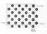
- FIG. 15 shows the first surface in the metal mask manufacturing process using the metal mask substrate of Example 1, after forming the first recess on the first surface and irradiating the first surface with irradiation light. It is the image which imaged the reflected light reflected in.
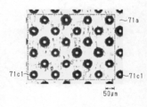
- FIG. 16 shows a first step of irradiating the first surface with irradiation light after forming the first recess on the first surface in the manufacturing process of the metal mask using the metal mask base material of Comparative Example 1. It is the image which imaged the reflected light reflected in.
- the adhesion between the metal mask substrate 11 and the first dry film resist 12 is enhanced. Therefore, in the plan view facing the first surface 11a, it is recognized that the size of the opening in each first recess 11c1 on the first surface 11a is substantially equal to the size of the opening in all other first recesses 11c1. It was.
- Example 1 the diameters of 24 first recesses were measured.
- Example 1 the diameter of the first recess 11c1 included in the region surrounded by the two-dot chain line in the first recess 11c1 shown in FIG. 15 is measured.
- Comparative Example 1 the first recess shown in FIG. The diameter of the 1st recessed part 71c1 contained in the area
- a first diameter that is a diameter in the vertical direction of the paper surface and a second diameter that is a diameter in the horizontal direction of the paper surface are measured, and for each first recess, the first diameter and the first diameter are measured.
- the average diameter which is the average value with the two diameters, was calculated.
- the first diameter, the second diameter, and the average diameter in Example 1 and the first diameter, the second diameter, and the average diameter in Comparative Example 1 were as shown in Table 4 below.
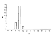
- the average diameter of the first recess 11c1 of Example 1 is 47.0 ⁇ m or more and 50.4 ⁇ m or less
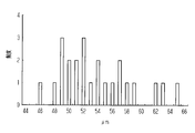
- the average diameter of the first recess 71c1 of Comparative Example 1 is 46.0 ⁇ m or more and 64.mu.m. It was found to be 9 ⁇ m or less.
- Example 1 the average value of the diameter in the opening of the first recess 11c1 in a plan view facing the surface of the metal mask base material 11 is A, and the value obtained by multiplying the standard deviation of the diameter by 3 is (B / A) ⁇ 100 (%) was calculated.
- (B / A) ⁇ 100 (%) is 8.2%
- (B / A) ⁇ 100 (%) is 6.6%
- the average diameter (B / A) ⁇ 100 (%) was found to be 5.9%.
- Example 1 the average value of the diameters of the openings of the first recesses 71c1 in plan view facing the surface 71a of the metal layer is A, and the value obtained by multiplying the standard deviation of the diameters by 3 is As B, (B / A) ⁇ 100 (%) was calculated. In the first diameter, (B / A) ⁇ 100 (%) is 30.3%, and in the second diameter, (B / A) ⁇ 100 (%) is 26.1%, and the average diameter (B / A) ⁇ 100 (%) was found to be 26.7%.
- Example 1 In Example 1, (B / A) ⁇ 100 (%) is 8.2% or less, that is, 10% or less. Therefore, the opening of the first concave portion 11c1 included in the metal mask base material 11, and thus the penetration included in the metal mask. It was found that the dimensional accuracy was high in the diameter at the opening of the hole. On the other hand, in Comparative Example 1, (B / A) ⁇ 100 (%) is 30.3% or less, and according to Example 1, the metal mask base material 11 has compared with Comparative Example 1. It was recognized that the dimensional accuracy was greatly increased in the diameter of the opening of the first recess 11c1, and hence the opening of the through hole of the metal mask.
- Example 1 For Example 1 and Comparative Example 1, a histogram showing the frequency of the average diameter of the first recesses every 2 ⁇ m and a histogram showing every 1 ⁇ m were prepared.
- each of several 1st recessed part 11c1 is made. It was observed that the shape was formed with high accuracy.
- the metal mask base material of Comparative Example 1 it is recognized that the shape accuracy is lowered in the plurality of first recesses 71c1 because the adhesion between the metal mask base material and the dry film resist is low. It was.
- Example 2 to Example 5 it was confirmed that a shape equivalent to the shape of the plurality of first recesses shown in FIG. 15 was obtained. That is, it was recognized that the adhesion between the metal layer 21 and the first dry film resist 12 was increased when the reflectance at regular reflection was 45.2% or more on one surface of the metal mask substrate 11.
- the second recess 11c2 is formed on the second surface 11b of the metal mask base material 11
- the following tendency is obtained as long as the reflectance in the regular reflection on the second surface 11b is included in the above-described range.
- the tendency which shows that the adhesiveness of the metal mask base material 11 and the 2nd dry film resist 13 is improved similarly to the time of forming the 1st recessed part 11c1 in the 1st surface 11a of the metal mask base material 11 is shown.
- the reflectance in regular reflection has a negative correlation with respect to each of the three-dimensional surface roughness Sa and the three-dimensional surface roughness Sz. If the reflectance in regular reflection is 45.2% or more, both the value of the three-dimensional surface roughness Sa and the value of the three-dimensional surface roughness Sz are the values for the dry film resist and the dry film resist. It was recognized that the adhesion at the interface with the metal mask base material was increased. That is, as the three-dimensional surface roughness Sa decreases, the reflectance in regular reflection increases, and as the three-dimensional surface roughness Sz decreases, the reflectance in regular reflection increases. It was recognized that
- the reflection at regular reflection is necessary to manage the state of the surface of the metal mask base material for dry film resist. Management using rate measurements is possible.
- the metal mask substrate for dry film resist As described above, according to one embodiment, the metal mask substrate for dry film resist, the method for managing the metal mask substrate for dry film resist, the metal mask, and the method for manufacturing the metal mask are listed below. An effect can be obtained.
- the reflectance in regular reflection is 45.2% or more, and therefore, at the interface between the first surface 11a of the metal mask substrate 11 and the first dry film resist 12. Adhesion can be increased.
- the relatively small reflectance is 45.2% or more, so the first surface 11a of the metal mask substrate 11 and the dry film resist 12 The adhesion at the interface can be further increased.
- the first surface 11a includes a portion where the second reflectance is 10.2% or more larger than the first reflectance, the adhesion at the interface between the first surface 11a and the dry film resist 12 is improved. And more preferable.
- the reflectance in regular reflection is 45.2% or more
- the three-dimensional surface roughness Sa is 0.11 ⁇ m or less
- the three-dimensional surface roughness Sz. Is 3.17 ⁇ m or less, the adhesion at the interface between the first dry film resist 12 and the first surface 11a is more reliably increased.
- the metal mask 60 formed from the metal mask base material 11 is applied to film formation on the glass substrate, that is, the shape
- the metal mask 60 with improved accuracy can be applied to film formation on a glass substrate.
- the material for forming the metal layer 21 may be a material other than Invar as long as it is a pure metal having a metallic luster on the surface or an alloy. Moreover, when the forming material of the metal layer 21 is a material other than Invar, the difference in linear expansion coefficient between the forming material of the metal layer 21 and the resin layer in contact with the metal layer 21 is different in the forming material of the metal layer 21. A resin smaller than the difference between the linear expansion coefficient and the linear expansion coefficient of polyimide may be used.
- the second reflectance on the second surface 11b may be larger than the first reflectance, and the first reflectance may be 45.2% or more.
- the second surface on the first surface 11a of the metal layer 21, the second surface has the same effect as when the second reflectance is larger than the first reflectance and the first reflectance is 45.2% or more. 11b can be obtained.
- the second surface 11b may include a portion where the difference obtained by subtracting the first reflectance from the second reflectance is 10.2% or more. According to such a configuration, it is possible to obtain the same effect on the second surface 11b as when the first surface 11a includes a portion in which the difference obtained by subtracting the first reflectance from the second reflectance is 10.2% or more. it can.
- the reflectance by regular reflection on the second surface 11b may be less than 45.2%. Even with such a configuration, at least the first surface 11 a can improve the adhesion between the metal layer 21 and the first dry film resist 12.
- the three-dimensional surface roughness measurement region is a very small region compared to the reflectance measurement region.
- the three-dimensional surface roughness Sz is 3.17 ⁇ m. The following is effective. It is also effective to set the three-dimensional surface roughness Sa to 0.11 ⁇ m or less.
- the three-dimensional surface roughness Sz on the first surface 11a of the metal mask base material 11 is larger than 3.17 ⁇ m.
- the reflectance in regular reflection is 45.2% or more, the effect according to the above (1) can be obtained.
- the 1st surface 11a of the metal mask base material 11 has surface roughness of the grade which cannot specify a rolling direction from the numerical value of 1st reflectance and 2nd reflectance, and 1st reflectance and 2nd If both of the reflectances are 45.2% or more, a portion where the difference obtained by subtracting the first reflectance from the second reflectance is 10.2% or more may not be included. Even if it is such a structure, the effect according to (1) mentioned above can be acquired.
- the 1st surface 11a of the metal mask base material 11 has surface roughness of the grade which cannot specify a rolling direction from the numerical value of 1st reflectance and 2nd reflectance, and 1st reflectance and 2nd If both reflectivities are 45.2% or more, a portion where the first reflectivity and the second reflectivity are the same or a portion where the first reflectivity is greater than the second reflectivity is included. Also good. Even if it is such a structure, the effect according to (1) mentioned above can be acquired.
- each through-hole 61c may be substantially the same throughout the thickness direction of the mask base 61.
- the cross-sectional area of each through-hole 61c may increase from the first mask surface 61a toward the second mask surface 61b in the thickness direction of the mask base 61, or from the first mask surface 61a to the second mask. It may be reduced toward the surface 61b.
- the metal mask 60 is not limited to the metal mask used when the organic EL element forming material is vapor-deposited on the glass substrate, and other materials such as when various metal materials are formed by vapor deposition or sputtering. It may be a metal mask for the purpose. In this case, the plurality of through holes 61c may be irregularly arranged in a plan view facing the first mask surface 61a.
- the resist used for etching the metal mask base material is not limited to the dry film resist described above, and may be a resist formed by applying a coating liquid for forming a resist to the metal mask base material. . That is, the resist may be disposed on the surface of the metal mask base material by application, or may be disposed on the surface of the metal mask base material by pasting. Even with such a resist, according to the above-described metal mask base material, when using a resist with low adhesion to the surface of the metal mask base material, it is possible to obtain the same effect as when using a dry film resist. Is possible.
Landscapes
- Chemical & Material Sciences (AREA)
- Engineering & Computer Science (AREA)
- Chemical Kinetics & Catalysis (AREA)
- Materials Engineering (AREA)
- Mechanical Engineering (AREA)
- Metallurgy (AREA)
- Organic Chemistry (AREA)
- Physics & Mathematics (AREA)
- Manufacturing & Machinery (AREA)
- General Chemical & Material Sciences (AREA)
- Optics & Photonics (AREA)
- General Physics & Mathematics (AREA)
- Health & Medical Sciences (AREA)
- Biochemistry (AREA)
- General Health & Medical Sciences (AREA)
- Immunology (AREA)
- Pathology (AREA)
- Analytical Chemistry (AREA)
- Life Sciences & Earth Sciences (AREA)
- Physical Vapour Deposition (AREA)
- Electroluminescent Light Sources (AREA)
Abstract
Description
上記構成によれば、ガラス基板の線膨張係数とインバーの線膨張係数とが同じ程度であるため、メタルマスク基材から形成されるメタルマスクをガラス基板に対する成膜に適用すること、すなわち、形状の精度が高められたメタルマスクをガラス基板に対する成膜に適用することが可能である。
図1から図4を参照して、ドライフィルムレジスト用メタルマスク基材の構成を説明する。
(反射率)(%)=
{(正反射における光の光量)/(入射光の光量)}×100 …(1)
メタルマスク基材11の第1面11aにおける反射率のうち、第1面11aに垂直な第1平面であって、圧延方向と直交する第1平面内での正反射における反射率が第1反射率である。また、第1面11aに垂直な方向であって、幅方向と直交する第2平面内での正反射における反射率が第2反射率である。第1面11aにおいて、第2反射率が第1反射率よりも大きく、第1反射率が45.2%以上である。
三次元表面粗さSa、および、三次元表面粗さSzは、ISO 25178に準拠する方法によって測定された値である。三次元表面粗さSaは、所定の面積を有する定義領域中の算術平均高さSaであり、三次元表面粗さSzは、所定の面積を有する定義領域中の最大高さSzである。
図2が示すように、金属層21は、第1面11aとは反対側の面である第2面11bを備えている。第1面11aは、第1ドライフィルムレジスト12が貼り付けられるように構成された金属製の表面であり、第2面11bは、レジストが配置されるように構成された金属製の表面、詳細には、第2ドライフィルムレジスト13が貼り付けられるように構成された金属製の表面である。メタルマスク形成用中間体10は、金属層21、第1ドライフィルムレジスト12、および、第2ドライフィルムレジスト13から構成されている。
図3が示すように、メタルマスク基材11は、金属層21と、金属層21に対して第1ドライフィルムレジスト12とは反対側に位置する樹脂層22とを備えてもよい。樹脂層22の線膨張係数と、金属層21の線膨張係数とは、温度の依存性として互いに同じ傾向を示し、かつ、線膨張係数の値が同じ程度であることが好ましい。金属層21は、例えばインバーから形成されたインバー層であり、樹脂層22は、例えばポリイミドから形成されたポリイミド層である。このメタルマスク基材11によれば、金属層21の線膨張係数と、樹脂層22の線膨張係数との差によって、メタルマスク基材11に反りが生じることが抑えられる。
図4が示すように、メタルマスク基材11は、金属層21と樹脂層22とに加えて、メタルマスク基材11の厚さ方向において、樹脂層22に対して金属層21とは反対側に位置する他の金属層23をさらに備えてもよい。このメタルマスク基材11では、メタルマスク基材11における第1面11aとは反対側の面であって、金属層23の含む面が第2面11bである。
図5を参照して、ドライフィルムレジスト用メタルマスク基材の管理方法を説明する。
図6および図7を参照して、ドライフィルムレジスト用メタルマスク基材の製造方法を説明する。
図8から図14を参照して、メタルマスクの製造方法を説明する。なお、以下では、メタルマスクを製造するために使用されるメタルマスク基材11が、1つの金属層21から構成される例、すなわち、図2を参照して説明された第1の形態を用いて説明する。また、図8から図13では、図示の便宜上から、メタルマスクに形成される複数の貫通孔のうち、1つの貫通孔のみを含む部分に対する工程図が示されている。
図15から図22を参照して、実施例を説明する。以下では、メタルマスク基材が1つの金属層から構成される例を説明する。
[正反射における反射率の最小値]
実施例1から実施例4、および、比較例1のメタルマスク基材の各々における反射率を以下の測定方法を用いて測定した。
なお、光源としてハロゲンランプを用い、受光部には、受光素子としてサイドオン型光電子増倍管を含む受光部を用いた。

実施例5のメタルマスク基材と比較例2のメタルマスク基材との各々において、4枚の試験片を準備した。このとき、実施例1と同様、実施例5のメタルマスク基材、および、比較例2のメタルマスク基材において、430mmの幅を有するメタルマスク基材の原反を準備し、原反の一部を500mmの長さで切り出した。そして、切り出したメタルマスク基材のうちの任意の4つの位置の各々から、1つの試験片を切り出した。なお、各試験片は、実施例1と同様、メタルマスク基材における幅方向に沿う長さが5cmであり、圧延方向に沿う長さが5cmである正方形形状を有する試験片とした。
各試験片において、第1反射率および第2反射率は、表2に示される値であった。

実施例1から実施例4、および、比較例1のメタルマスク基材の各々について、三次元表面粗さSa、および、三次元表面粗さSzを以下の測定方法を用いて測定した。
なお、三次元表面粗さSaおよび三次元表面粗さSzは、ISO 25178に準拠する方向によって測定した。

図15は、実施例1のメタルマスク基材を用いたメタルマスクの製造工程において、第1面に第1凹部を形成した後に、第1面に対して照射光を照射して、第1面にて反射された反射光を撮像した画像である。
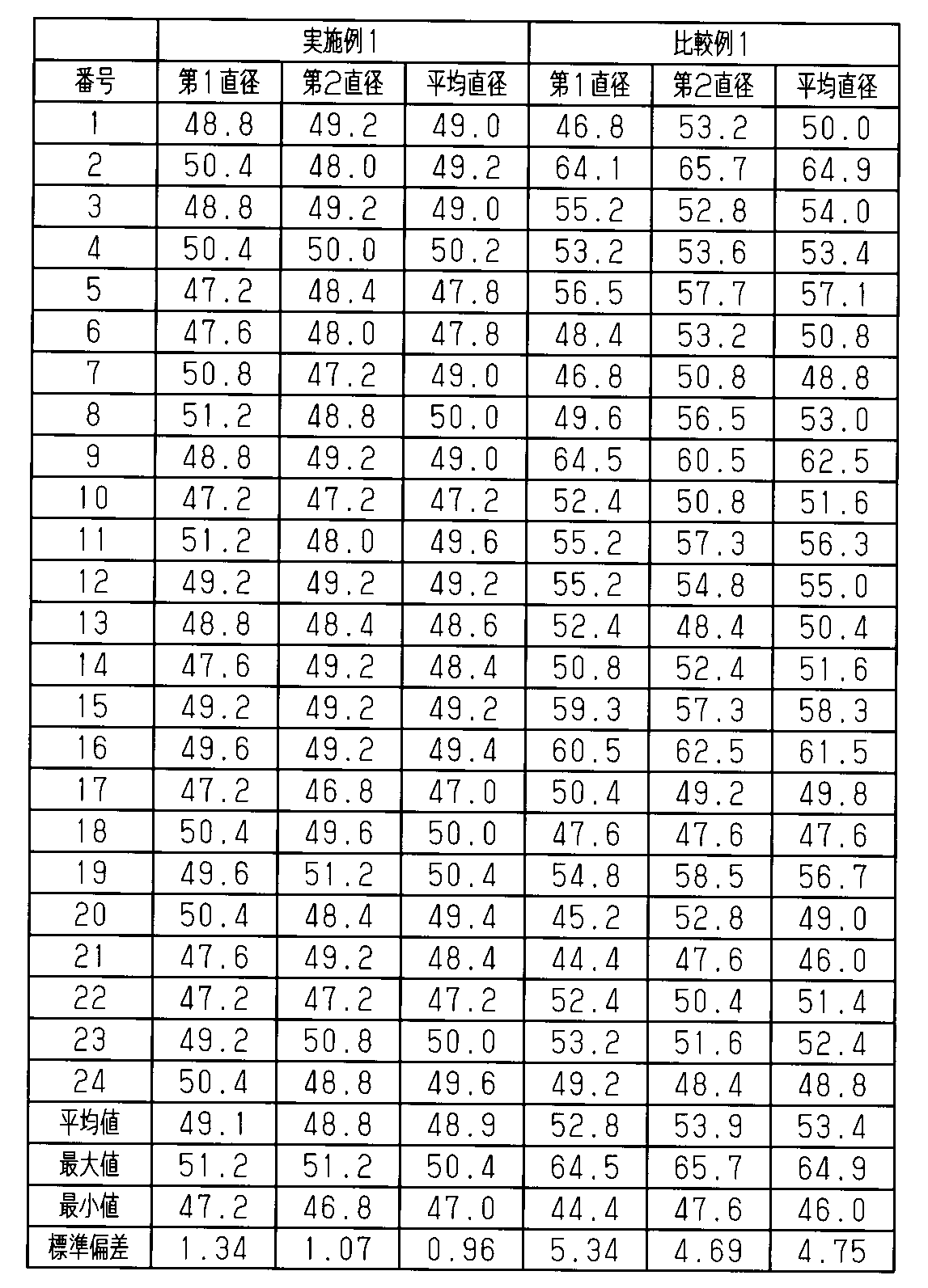
[反射率と三次元表面粗さSa]
正反射における反射率の最小値と、三次元表面粗さSaの最大値との相関関係を回帰分析による解析結果として以下に示す。なお、回帰分析には、実施例1から実施例4、および、比較例1の測定結果を用いた。また、説明変数を三次元表面粗さSaとし、被説明変数を正反射における反射率とし、最小二乗法を用いて、正反射における反射率の最小値と三次元表面粗さSaの最大値との間における回帰式を算出した。
正反射における反射率の最小値と、三次元表面粗さSzの最大値との相関関係を回帰分析による解析結果として以下に示す。なお、回帰分析には、実施例1から実施例4、および、比較例1の測定結果を用いた。また、説明変数を三次元表面粗さSzとし、被説明変数を正反射における反射率とし、最小二乗法を用いて、正反射における反射率の最小値と三次元表面粗さSzの最大値との間における回帰式を算出した。
・金属層21の形成材料は、表面に金属光沢を有する純粋な金属、あるいは、合金であれば、インバー以外の材料であってもよい。また、金属層21の形成材料がインバー以外の材料であるとき、金属層21に接する樹脂層として、金属層21の形成材料との間における線膨張係数の差が、金属層21の形成材料における線膨張係数と、ポリイミドにおける線膨張係数との差よりも小さい樹脂が用いられてもよい。
Claims (11)
- レジストが配置されるように構成された金属製の表面を備え、
前記表面に入射した光の正反射における反射率が、45.2%以上である
メタルマスク基材。 - 前記メタルマスク基材の圧延方向と直交する方向が幅方向であり、
前記表面に垂直な第1平面であって、前記圧延方向と直交する前記第1平面内での前記正反射における反射率が第1反射率であり、
前記表面に垂直な第2平面であって、前記幅方向と直交する前記第2平面内での前記正反射における反射率が第2反射率であり、
前記第2反射率が前記第1反射率よりも大きく、
前記第1反射率が、45.2%以上である
請求項1に記載のメタルマスク基材。 - 前記表面は、前記第2反射率から前記第1反射率を引いた差が10.2%以上である部分を含む
請求項2に記載のメタルマスク基材。 - 前記表面において、
三次元表面粗さSaが0.11μm以下であり、
三次元表面粗さSzが3.17μm以下である
請求項1から3のいずれか一項に記載のメタルマスク基材。 - 前記表面が第1面であり、
前記レジストが第1レジストであり、
前記第1面とは反対側の面であって、第2レジストが配置されるように構成された金属製の第2面をさらに備え、
前記第2面に入射した光の正反射における反射率が、45.2%以上である
請求項1から4のいずれか一項に記載のメタルマスク基材。 - 前記表面は、インバー製である
請求項1から5のいずれか一項に記載のメタルマスク基材。 - 前記レジストが、ドライフィルムレジストであり、
前記表面が、前記ドライフィルムレジストが貼り付けられるように構成されている
請求項1から6のいずれか一項に記載のメタルマスク基材。 - レジストが配置されるように構成された金属製の表面を備えるメタルマスク基材を準備することと、
前記表面に光を入射させることと、
前記表面に入射した光のうち、前記表面にて正反射した光の光量を測定することと、
前記表面に入射した光の光量に対する前記正反射した光の光量の比として、前記正反射における反射率を算出することと、
前記正反射における反射率が、45.2%以上であるか否かを判断することと、を備える
メタルマスク基材の管理方法。 - 前記レジストが、ドライフィルムレジストであり、
前記表面が、前記ドライフィルムレジストが貼り付けられるように構成されている
請求項8に記載のメタルマスク基材の管理方法。 - 金属製の表面を有したメタルマスク基体を備えるメタルマスクであって、
前記メタルマスク基体は、前記メタルマスク基体の厚さ方向に沿って前記メタルマスク基体を貫通するとともに、前記表面に開口を有した複数の貫通孔を備え、
前記表面と対向する平面視での前記開口の寸法における平均値をAとし、前記寸法の標準偏差に3を掛けた値をBとするとき、(B/A)×100(%)が10%以下である
メタルマスク。 - レジストが配置されるように構成された金属製の表面を備え、前記表面の三次元表面粗さSaが0.11μm以下であり、前記表面の三次元表面粗さSzが3.17μm以下であるメタルマスク基材を準備することと、
前記表面にレジストを配置することと、
前記メタルマスク基材に前記メタルマスク基材の厚さ方向に沿って窪み、かつ、前記表面に開口を有した複数の凹部を形成するための貫通孔を前記レジストに形成することと、
前記レジストを介して、前記メタルマスク基材に複数の前記凹部を形成することと、を備え、
前記メタルマスク基材に複数の前記凹部を形成することでは、前記表面と対向する平面視での前記開口の寸法における平均値をAとし、前記寸法の標準偏差に3を掛けた値をBとするとき、(B/A)×100(%)が10%以下となるように前記メタルマスク基材に複数の前記凹部を形成する
メタルマスクの製造方法。
Priority Applications (6)
| Application Number | Priority Date | Filing Date | Title |
|---|---|---|---|
| JP2016553484A JP6848433B2 (ja) | 2015-07-17 | 2016-03-22 | メタルマスク基材、メタルマスク基材の管理方法、メタルマスク、および、メタルマスクの製造方法 |
| KR1020177024436A KR101810824B1 (ko) | 2015-07-17 | 2016-03-22 | 메탈 마스크 기재, 메탈 마스크 기재의 관리 방법, 메탈 마스크, 및, 메탈 마스크의 제조 방법 |
| DE112016003230.7T DE112016003230T5 (de) | 2015-07-17 | 2016-03-22 | Metallmaskensubstrat, metallmaskensubstratkontrollverfahren, metallmaske und metallmaskenherstellungsverfahren |
| CN201680013004.0A CN107406964B (zh) | 2015-07-17 | 2016-03-22 | 金属掩模基材、金属掩模基材的管理方法、金属掩模以及金属掩模的制造方法 |
| KR1020177035822A KR102341450B1 (ko) | 2015-07-17 | 2016-03-22 | 메탈 마스크 기재, 메탈 마스크 기재의 관리 방법, 메탈 마스크, 및, 메탈 마스크의 제조 방법 |
| US15/786,463 US10273569B2 (en) | 2015-07-17 | 2017-10-17 | Metal mask substrate, metal mask substrate control method, metal mask, and metal mask production method |
Applications Claiming Priority (4)
| Application Number | Priority Date | Filing Date | Title |
|---|---|---|---|
| JP2015-143509 | 2015-07-17 | ||
| JP2015143509 | 2015-07-17 | ||
| JP2015-171440 | 2015-08-31 | ||
| JP2015171440 | 2015-08-31 |
Related Child Applications (1)
| Application Number | Title | Priority Date | Filing Date |
|---|---|---|---|
| US15/786,463 Continuation US10273569B2 (en) | 2015-07-17 | 2017-10-17 | Metal mask substrate, metal mask substrate control method, metal mask, and metal mask production method |
Publications (1)
| Publication Number | Publication Date |
|---|---|
| WO2017013904A1 true WO2017013904A1 (ja) | 2017-01-26 |
Family
ID=57833862
Family Applications (1)
| Application Number | Title | Priority Date | Filing Date |
|---|---|---|---|
| PCT/JP2016/059042 Ceased WO2017013904A1 (ja) | 2015-07-17 | 2016-03-22 | メタルマスク基材、メタルマスク基材の管理方法、メタルマスク、および、メタルマスクの製造方法 |
Country Status (7)
| Country | Link |
|---|---|
| US (1) | US10273569B2 (ja) |
| JP (3) | JP6848433B2 (ja) |
| KR (2) | KR101810824B1 (ja) |
| CN (2) | CN109440062B (ja) |
| DE (1) | DE112016003230T5 (ja) |
| TW (2) | TWI626505B (ja) |
| WO (1) | WO2017013904A1 (ja) |
Cited By (3)
| Publication number | Priority date | Publication date | Assignee | Title |
|---|---|---|---|---|
| CN109778115A (zh) * | 2017-11-14 | 2019-05-21 | 大日本印刷株式会社 | 制造蒸镀掩模的金属板及其检查方法和制造方法、蒸镀掩模及其制造方法和蒸镀掩模装置 |
| EP4451058A2 (en) | 2023-04-18 | 2024-10-23 | Dai Nippon Printing Co., Ltd. | Metal sheet, inspecting method for metal sheet, manufacturing method for metal sheet, mask, mask device, and manufacturing method for mask |
| US12227823B2 (en) | 2018-11-13 | 2025-02-18 | Dai Nippon Printing Co., Ltd. | Metal plate for producing vapor deposition masks, production method for metal plates, vapor deposition mask, production method for vapor deposition mask, and vapor deposition mask device comprising vapor deposition mask |
Families Citing this family (17)
| Publication number | Priority date | Publication date | Assignee | Title |
|---|---|---|---|---|
| KR102509663B1 (ko) | 2015-07-17 | 2023-03-14 | 도판 인사츠 가부시키가이샤 | 메탈 마스크용 기재의 제조 방법, 증착용 메탈 마스크의 제조 방법, 메탈 마스크용 기재, 및, 증착용 메탈 마스크 |
| KR102071840B1 (ko) * | 2015-07-17 | 2020-01-31 | 도판 인사츠 가부시키가이샤 | 메탈 마스크 기재, 메탈 마스크, 및 메탈 마스크의 제조 방법 |
| KR102330373B1 (ko) * | 2017-03-14 | 2021-11-23 | 엘지이노텍 주식회사 | 금속판, 증착용 마스크 및 이의 제조방법 |
| KR102595424B1 (ko) * | 2017-09-07 | 2023-10-30 | 엘지이노텍 주식회사 | Oled 화소 증착을 위한 금속재의 증착용 마스크의 제조방법 |
| CN114899345B (zh) * | 2017-09-07 | 2026-04-24 | Lg伊诺特有限公司 | 用于制造有机发光二极管沉积掩模的方法 |
| CN112981319B (zh) | 2017-09-15 | 2022-12-20 | 凸版印刷株式会社 | 蒸镀掩模、带玻璃基板的蒸镀掩模及带玻璃基板的掩模片材 |
| KR102816248B1 (ko) * | 2018-11-14 | 2025-06-05 | 삼성디스플레이 주식회사 | 마스크 및 마스크 제조 방법 |
| TWI707965B (zh) * | 2019-09-27 | 2020-10-21 | 旭暉應用材料股份有限公司 | 金屬遮罩 |
| CN112825348A (zh) * | 2019-11-20 | 2021-05-21 | 旭晖应用材料股份有限公司 | 用于蒸镀制程形成微小图案镀膜的金属遮罩及其制法 |
| JP2022168819A (ja) * | 2021-04-26 | 2022-11-08 | 富士フイルム株式会社 | 蒸着マスク製造用転写フィルム、蒸着マスク及び蒸着マスクの製造方法 |
| CN113259569B (zh) | 2021-05-25 | 2024-09-06 | 昆山联滔电子有限公司 | 摄像头遮蔽器 |
| TWI777614B (zh) * | 2021-06-11 | 2022-09-11 | 達運精密工業股份有限公司 | 金屬遮罩及其製造方法 |
| TWI772066B (zh) | 2021-06-16 | 2022-07-21 | 達運精密工業股份有限公司 | 金屬遮罩基材的製備方法 |
| KR102927491B1 (ko) * | 2023-01-18 | 2026-02-12 | 한양대학교 산학협력단 | 멀티 레이어 euvl 블랭크 마스크의 러프니스 분석장치 및 그 방법 |
| KR20240167225A (ko) * | 2023-05-19 | 2024-11-26 | 엘지이노텍 주식회사 | 금속판 및 이를 포함하는 증착용 마스크 |
| WO2025110102A1 (ja) * | 2023-11-22 | 2025-05-30 | 大日本印刷株式会社 | マスク及びマスクの製造方法 |
| JP2025185884A (ja) * | 2024-06-11 | 2025-12-23 | Toppanホールディングス株式会社 | メタルマスク用基材の選択方法、メタルマスク用基材、およびメタルマスク |
Citations (6)
| Publication number | Priority date | Publication date | Assignee | Title |
|---|---|---|---|---|
| JP2005076068A (ja) * | 2003-08-29 | 2005-03-24 | Canon Components Inc | 電鋳法による薄膜部材の製造方法 |
| JP2006233285A (ja) * | 2005-02-25 | 2006-09-07 | Toray Ind Inc | 蒸着マスク及び蒸着マスクを用いた有機el素子の製造方法 |
| JP2008041553A (ja) * | 2006-08-09 | 2008-02-21 | Sony Corp | 蒸着用マスク及び蒸着用マスクの製造方法 |
| JP2011166018A (ja) * | 2010-02-12 | 2011-08-25 | Jx Nippon Mining & Metals Corp | プリント配線板用銅箔 |
| JP5641462B1 (ja) * | 2014-05-13 | 2014-12-17 | 大日本印刷株式会社 | 金属板、金属板の製造方法、および金属板を用いてマスクを製造する方法 |
| JP2015129334A (ja) * | 2014-01-08 | 2015-07-16 | 大日本印刷株式会社 | 積層マスクの製造方法、積層マスクおよび保護フィルム付き積層マスク |
Family Cites Families (35)
| Publication number | Priority date | Publication date | Assignee | Title |
|---|---|---|---|---|
| JP2534589B2 (ja) | 1991-01-21 | 1996-09-18 | 東洋鋼鈑株式会社 | 薄肉化深絞り缶用ポリエステル樹脂被覆鋼板および原板 |
| JP2853069B2 (ja) * | 1991-12-26 | 1999-02-03 | 日本鋼管株式会社 | Fe−Ni系シャドウマスク用薄板およびその製造方法 |
| JP3487471B2 (ja) * | 1996-01-30 | 2004-01-19 | 日立金属株式会社 | エッチング加工性に優れたFe−Ni系合金薄板 |
| JPH11140667A (ja) * | 1997-11-13 | 1999-05-25 | Dainippon Printing Co Ltd | エッチング用基材、エッチング加工方法およびエッチング加工製品 |
| JP3749083B2 (ja) * | 2000-04-25 | 2006-02-22 | 株式会社ルネサステクノロジ | 電子装置の製造方法 |
| JP2002151841A (ja) | 2000-11-13 | 2002-05-24 | Ibiden Co Ltd | 多層プリント配線板の製造方法 |
| JP4390418B2 (ja) * | 2001-02-14 | 2009-12-24 | Hoya株式会社 | Euv露光用反射型マスクブランクおよびeuv露光用反射型マスク並びに半導体の製造方法 |
| JP4429539B2 (ja) | 2001-02-16 | 2010-03-10 | 古河電気工業株式会社 | ファインパターン用電解銅箔 |
| TW583688B (en) * | 2002-02-21 | 2004-04-11 | Dainippon Printing Co Ltd | Electromagnetic shielding sheet and method of producing the same |
| KR100813832B1 (ko) | 2002-05-31 | 2008-03-17 | 삼성에스디아이 주식회사 | 증착용 마스크 프레임 조립체와 이의 제조방법 |
| US20040017563A1 (en) * | 2002-07-25 | 2004-01-29 | James Lawrence H. | Method and apparatus for volume and density measurements |
| US7314688B2 (en) * | 2002-09-11 | 2008-01-01 | Hoya Corporation | Method of producing a reflection mask blank, method of producing a reflection mask, and method of producing a semiconductor device |
| JP3683261B2 (ja) * | 2003-03-03 | 2005-08-17 | Hoya株式会社 | 擬似欠陥を有する反射型マスクブランクス及びその製造方法、擬似欠陥を有する反射型マスク及びその製造方法、並びに擬似欠陥を有する反射型マスクブランクス又は反射型マスクの製造用基板 |
| JP3809531B2 (ja) | 2003-03-17 | 2006-08-16 | 太陽化学工業株式会社 | メタルマスク及びレーザ加工法によるメタルマスクの製造方法 |
| WO2004101857A2 (en) * | 2003-05-07 | 2004-11-25 | Microfabrica Inc. | Methods and apparatus for forming multi-layer structures using adhered masks |
| US7495182B2 (en) * | 2004-01-30 | 2009-02-24 | Dai Nippon Printing Co., Ltd. | Electromagnetic wave shielding sheet and process for producing the same |
| JP2007187952A (ja) * | 2006-01-16 | 2007-07-26 | Sumitomo Chemical Co Ltd | 防眩フィルム、その製造方法、そのための金型の製造方法、及び表示装置 |
| US8532984B2 (en) * | 2006-07-31 | 2013-09-10 | Qualcomm Incorporated | Systems, methods, and apparatus for wideband encoding and decoding of active frames |
| JP4869129B2 (ja) * | 2007-03-30 | 2012-02-08 | Hoya株式会社 | パターン欠陥検査方法 |
| JP2009127105A (ja) | 2007-11-27 | 2009-06-11 | Seiko Instruments Inc | 電鋳部品の製造方法 |
| JP5294072B2 (ja) | 2009-03-18 | 2013-09-18 | 日立金属株式会社 | エッチング加工用素材の製造方法及びエッチング加工用素材 |
| JP2011034681A (ja) * | 2009-07-29 | 2011-02-17 | Hitachi Displays Ltd | 金属加工方法、金属マスク製造方法及び有機el表示装置製造方法 |
| ES2430641T3 (es) | 2010-10-22 | 2013-11-21 | Hydro Aluminium Rolled Products Gmbh | Banda litográfica para desbastado electroquímico y método para su fabricación |
| JP5958804B2 (ja) | 2012-03-30 | 2016-08-02 | 株式会社ブイ・テクノロジー | 蒸着マスク、蒸着マスクの製造方法及び有機el表示装置の製造方法 |
| US9966216B2 (en) * | 2011-11-04 | 2018-05-08 | Princeton University | Photo-electron source assembly with scaled nanostructures and nanoscale metallic photonic resonant cavity, and method of making same |
| CN105779934B (zh) | 2012-01-12 | 2020-05-22 | 大日本印刷株式会社 | 蒸镀掩模的制造方法及有机半导体元件的制造方法 |
| CN103205680A (zh) * | 2012-01-16 | 2013-07-17 | 昆山允升吉光电科技有限公司 | 用镍铁合金制备的蒸镀用金属掩模板 |
| TWI596385B (zh) * | 2012-02-13 | 2017-08-21 | 東麗股份有限公司 | 反射膜 |
| JP2013245392A (ja) | 2012-05-29 | 2013-12-09 | V Technology Co Ltd | 蒸着マスク及び蒸着マスクの製造方法 |
| KR101707345B1 (ko) | 2012-09-04 | 2017-02-15 | 신닛테츠스미킨 카부시키카이샤 | 정밀 가공용 스테인리스 강판 및 그 제조 방법 |
| JP5382259B1 (ja) * | 2013-01-10 | 2014-01-08 | 大日本印刷株式会社 | 金属板、金属板の製造方法、および金属板を用いて蒸着マスクを製造する方法 |
| JP6403969B2 (ja) | 2013-03-29 | 2018-10-10 | Jx金属株式会社 | キャリア付銅箔、プリント配線板、銅張積層板、電子機器及びプリント配線板の製造方法 |
| JP5455099B1 (ja) | 2013-09-13 | 2014-03-26 | 大日本印刷株式会社 | 金属板、金属板の製造方法、および金属板を用いてマスクを製造する方法 |
| JP5780350B2 (ja) | 2013-11-14 | 2015-09-16 | 大日本印刷株式会社 | 蒸着マスク、フレーム付き蒸着マスク、及び有機半導体素子の製造方法 |
| JP6357777B2 (ja) | 2014-01-08 | 2018-07-18 | 大日本印刷株式会社 | 積層マスクの製造方法 |
-
2016
- 2016-03-22 KR KR1020177024436A patent/KR101810824B1/ko active Active
- 2016-03-22 DE DE112016003230.7T patent/DE112016003230T5/de active Pending
- 2016-03-22 WO PCT/JP2016/059042 patent/WO2017013904A1/ja not_active Ceased
- 2016-03-22 CN CN201811389315.4A patent/CN109440062B/zh active Active
- 2016-03-22 CN CN201680013004.0A patent/CN107406964B/zh active Active
- 2016-03-22 JP JP2016553484A patent/JP6848433B2/ja active Active
- 2016-03-22 KR KR1020177035822A patent/KR102341450B1/ko active Active
- 2016-06-20 TW TW105119259A patent/TWI626505B/zh active
- 2016-06-20 TW TW107111905A patent/TWI700548B/zh active
- 2016-08-31 JP JP2016170240A patent/JP6090619B2/ja active Active
-
2017
- 2017-10-17 US US15/786,463 patent/US10273569B2/en active Active
-
2020
- 2020-12-01 JP JP2020199747A patent/JP7207389B2/ja active Active
Patent Citations (6)
| Publication number | Priority date | Publication date | Assignee | Title |
|---|---|---|---|---|
| JP2005076068A (ja) * | 2003-08-29 | 2005-03-24 | Canon Components Inc | 電鋳法による薄膜部材の製造方法 |
| JP2006233285A (ja) * | 2005-02-25 | 2006-09-07 | Toray Ind Inc | 蒸着マスク及び蒸着マスクを用いた有機el素子の製造方法 |
| JP2008041553A (ja) * | 2006-08-09 | 2008-02-21 | Sony Corp | 蒸着用マスク及び蒸着用マスクの製造方法 |
| JP2011166018A (ja) * | 2010-02-12 | 2011-08-25 | Jx Nippon Mining & Metals Corp | プリント配線板用銅箔 |
| JP2015129334A (ja) * | 2014-01-08 | 2015-07-16 | 大日本印刷株式会社 | 積層マスクの製造方法、積層マスクおよび保護フィルム付き積層マスク |
| JP5641462B1 (ja) * | 2014-05-13 | 2014-12-17 | 大日本印刷株式会社 | 金属板、金属板の製造方法、および金属板を用いてマスクを製造する方法 |
Cited By (14)
| Publication number | Priority date | Publication date | Assignee | Title |
|---|---|---|---|---|
| US11237481B2 (en) | 2017-11-14 | 2022-02-01 | Dai Nippon Printing Co., Ltd. | Metal plate for manufacturing deposition mask and manufacturing method for metal plate, and deposition mask and manufacturing method for deposition mask |
| US11733607B2 (en) | 2017-11-14 | 2023-08-22 | Dai Nippon Printing Co., Ltd. | Metal plate for producing vapor deposition masks, inspection method for metal plates, production method for metal plates, vapor deposition mask, vapor deposition mask device, and production method for vapor deposition masks |
| JPWO2019098168A1 (ja) * | 2017-11-14 | 2019-11-14 | 大日本印刷株式会社 | 蒸着マスクを製造するための金属板、金属板の検査方法、金属板の製造方法、蒸着マスク、蒸着マスク装置及び蒸着マスクの製造方法 |
| JP2019214788A (ja) * | 2017-11-14 | 2019-12-19 | 大日本印刷株式会社 | 蒸着マスクを製造するための金属板、金属板の検査方法、金属板の製造方法、蒸着マスク、蒸着マスク装置及び蒸着マスクの製造方法 |
| KR20200086691A (ko) * | 2017-11-14 | 2020-07-17 | 다이니폰 인사츠 가부시키가이샤 | 증착 마스크를 제조하기 위한 금속판, 금속판의 검사 방법, 금속판의 제조 방법, 증착 마스크, 증착 마스크 장치 및 증착 마스크의 제조 방법 |
| JP2020190033A (ja) * | 2017-11-14 | 2020-11-26 | 大日本印刷株式会社 | 蒸着マスクを製造するための金属板、金属板の検査方法、金属板の製造方法、蒸着マスク、蒸着マスク装置及び蒸着マスクの製造方法 |
| KR102591494B1 (ko) * | 2017-11-14 | 2023-10-20 | 다이니폰 인사츠 가부시키가이샤 | 증착 마스크를 제조하기 위한 금속판, 금속판의 검사 방법, 금속판의 제조 방법, 증착 마스크, 증착 마스크 장치 및 증착 마스크의 제조 방법 |
| CN109778115A (zh) * | 2017-11-14 | 2019-05-21 | 大日本印刷株式会社 | 制造蒸镀掩模的金属板及其检查方法和制造方法、蒸镀掩模及其制造方法和蒸镀掩模装置 |
| WO2019098168A1 (ja) * | 2017-11-14 | 2019-05-23 | 大日本印刷株式会社 | 蒸着マスクを製造するための金属板、金属板の検査方法、金属板の製造方法、蒸着マスク、蒸着マスク装置及び蒸着マスクの製造方法 |
| US12117727B2 (en) | 2017-11-14 | 2024-10-15 | Dai Nippon Printing Co., Ltd. | Metal plate for manufacturing deposition mask and manufacturing method for metal plate, and deposition mask and manufacturing method for deposition mask |
| US12540385B2 (en) | 2017-11-14 | 2026-02-03 | Dai Nippon Printing Co., Ltd. | Production method for metal plates for vapor deposition masks |
| US12227823B2 (en) | 2018-11-13 | 2025-02-18 | Dai Nippon Printing Co., Ltd. | Metal plate for producing vapor deposition masks, production method for metal plates, vapor deposition mask, production method for vapor deposition mask, and vapor deposition mask device comprising vapor deposition mask |
| KR20240154439A (ko) | 2023-04-18 | 2024-10-25 | 다이니폰 인사츠 가부시키가이샤 | 금속판, 금속판의 제조 방법, 마스크, 마스크 장치 및 마스크의 제조 방법 |
| EP4451058A2 (en) | 2023-04-18 | 2024-10-23 | Dai Nippon Printing Co., Ltd. | Metal sheet, inspecting method for metal sheet, manufacturing method for metal sheet, mask, mask device, and manufacturing method for mask |
Also Published As
| Publication number | Publication date |
|---|---|
| TW201708936A (zh) | 2017-03-01 |
| US10273569B2 (en) | 2019-04-30 |
| TWI626505B (zh) | 2018-06-11 |
| TW201830126A (zh) | 2018-08-16 |
| CN109440062B (zh) | 2021-02-05 |
| CN107406964B (zh) | 2018-12-18 |
| JP2021042478A (ja) | 2021-03-18 |
| JP6848433B2 (ja) | 2021-03-24 |
| JP2017043848A (ja) | 2017-03-02 |
| JP6090619B2 (ja) | 2017-03-08 |
| KR20180020973A (ko) | 2018-02-28 |
| JP7207389B2 (ja) | 2023-01-18 |
| TWI700548B (zh) | 2020-08-01 |
| JPWO2017013904A1 (ja) | 2018-04-26 |
| DE112016003230T5 (de) | 2018-04-19 |
| KR102341450B1 (ko) | 2021-12-21 |
| KR20170105120A (ko) | 2017-09-18 |
| KR101810824B1 (ko) | 2017-12-19 |
| CN107406964A (zh) | 2017-11-28 |
| US20180066352A1 (en) | 2018-03-08 |
| CN109440062A (zh) | 2019-03-08 |
Similar Documents
| Publication | Publication Date | Title |
|---|---|---|
| JP6090619B2 (ja) | メタルマスク基材、および、メタルマスク基材の管理方法 | |
| JP7226459B2 (ja) | メタルマスク基材、および、メタルマスクの製造方法 | |
| JP2020190033A (ja) | 蒸着マスクを製造するための金属板、金属板の検査方法、金属板の製造方法、蒸着マスク、蒸着マスク装置及び蒸着マスクの製造方法 | |
| JP2019214788A5 (ja) | ||
| CN102205671B (zh) | 测量材料表面形变的简易贴及其制作方法 | |
| US9520335B2 (en) | Wavelength selective heat radiation material selectively radiating heat radiation light corresponding to infrared ray transmission wavelength region of resin member and method for manufacturing the same | |
| JP5925365B1 (ja) | 光学式エンコーダ用格子板および光学式エンコーダ用格子板の製造方法 | |
| US12024780B2 (en) | Method of preparing metal mask substrate |
Legal Events
| Date | Code | Title | Description |
|---|---|---|---|
| ENP | Entry into the national phase |
Ref document number: 2016553484 Country of ref document: JP Kind code of ref document: A |
|
| 121 | Ep: the epo has been informed by wipo that ep was designated in this application |
Ref document number: 16827469 Country of ref document: EP Kind code of ref document: A1 |
|
| ENP | Entry into the national phase |
Ref document number: 20177024436 Country of ref document: KR Kind code of ref document: A |
|
| WWE | Wipo information: entry into national phase |
Ref document number: 112016003230 Country of ref document: DE |
|
| 122 | Ep: pct application non-entry in european phase |
Ref document number: 16827469 Country of ref document: EP Kind code of ref document: A1 |