WO2017010311A1 - 固体撮像素子、製造方法、および電子機器 - Google Patents
固体撮像素子、製造方法、および電子機器 Download PDFInfo
- Publication number
- WO2017010311A1 WO2017010311A1 PCT/JP2016/069592 JP2016069592W WO2017010311A1 WO 2017010311 A1 WO2017010311 A1 WO 2017010311A1 JP 2016069592 W JP2016069592 W JP 2016069592W WO 2017010311 A1 WO2017010311 A1 WO 2017010311A1
- Authority
- WO
- WIPO (PCT)
- Prior art keywords
- trench structure
- semiconductor substrate
- electrode
- solid
- state imaging
- Prior art date
- Legal status (The legal status is an assumption and is not a legal conclusion. Google has not performed a legal analysis and makes no representation as to the accuracy of the status listed.)
- Ceased
Links
Images











Classifications
-
- H—ELECTRICITY
- H10—SEMICONDUCTOR DEVICES; ELECTRIC SOLID-STATE DEVICES NOT OTHERWISE PROVIDED FOR
- H10W—GENERIC PACKAGES, INTERCONNECTIONS, CONNECTORS OR OTHER CONSTRUCTIONAL DETAILS OF DEVICES COVERED BY CLASS H10
- H10W90/00—Package configurations
-
- H—ELECTRICITY
- H04—ELECTRIC COMMUNICATION TECHNIQUE
- H04N—PICTORIAL COMMUNICATION, e.g. TELEVISION
- H04N25/00—Circuitry of solid-state image sensors [SSIS]; Control thereof
- H04N25/70—SSIS architectures; Circuits associated therewith
-
- H—ELECTRICITY
- H04—ELECTRIC COMMUNICATION TECHNIQUE
- H04N—PICTORIAL COMMUNICATION, e.g. TELEVISION
- H04N25/00—Circuitry of solid-state image sensors [SSIS]; Control thereof
- H04N25/70—SSIS architectures; Circuits associated therewith
- H04N25/76—Addressed sensors, e.g. MOS or CMOS sensors
-
- H—ELECTRICITY
- H10—SEMICONDUCTOR DEVICES; ELECTRIC SOLID-STATE DEVICES NOT OTHERWISE PROVIDED FOR
- H10F—INORGANIC SEMICONDUCTOR DEVICES SENSITIVE TO INFRARED RADIATION, LIGHT, ELECTROMAGNETIC RADIATION OF SHORTER WAVELENGTH OR CORPUSCULAR RADIATION
- H10F39/00—Integrated devices, or assemblies of multiple devices, comprising at least one element covered by group H10F30/00, e.g. radiation detectors comprising photodiode arrays
- H10F39/011—Manufacture or treatment of image sensors covered by group H10F39/12
- H10F39/014—Manufacture or treatment of image sensors covered by group H10F39/12 of CMOS image sensors
-
- H—ELECTRICITY
- H10—SEMICONDUCTOR DEVICES; ELECTRIC SOLID-STATE DEVICES NOT OTHERWISE PROVIDED FOR
- H10F—INORGANIC SEMICONDUCTOR DEVICES SENSITIVE TO INFRARED RADIATION, LIGHT, ELECTROMAGNETIC RADIATION OF SHORTER WAVELENGTH OR CORPUSCULAR RADIATION
- H10F39/00—Integrated devices, or assemblies of multiple devices, comprising at least one element covered by group H10F30/00, e.g. radiation detectors comprising photodiode arrays
- H10F39/10—Integrated devices
- H10F39/12—Image sensors
- H10F39/18—Complementary metal-oxide-semiconductor [CMOS] image sensors; Photodiode array image sensors
- H10F39/182—Colour image sensors
- H10F39/1825—Multicolour image sensors having stacked structure, e.g. NPN, NPNPN or multiple quantum well [MQW] structures
-
- H—ELECTRICITY
- H10—SEMICONDUCTOR DEVICES; ELECTRIC SOLID-STATE DEVICES NOT OTHERWISE PROVIDED FOR
- H10F—INORGANIC SEMICONDUCTOR DEVICES SENSITIVE TO INFRARED RADIATION, LIGHT, ELECTROMAGNETIC RADIATION OF SHORTER WAVELENGTH OR CORPUSCULAR RADIATION
- H10F39/00—Integrated devices, or assemblies of multiple devices, comprising at least one element covered by group H10F30/00, e.g. radiation detectors comprising photodiode arrays
- H10F39/10—Integrated devices
- H10F39/12—Image sensors
- H10F39/191—Photoconductor image sensors
-
- H—ELECTRICITY
- H10—SEMICONDUCTOR DEVICES; ELECTRIC SOLID-STATE DEVICES NOT OTHERWISE PROVIDED FOR
- H10F—INORGANIC SEMICONDUCTOR DEVICES SENSITIVE TO INFRARED RADIATION, LIGHT, ELECTROMAGNETIC RADIATION OF SHORTER WAVELENGTH OR CORPUSCULAR RADIATION
- H10F39/00—Integrated devices, or assemblies of multiple devices, comprising at least one element covered by group H10F30/00, e.g. radiation detectors comprising photodiode arrays
- H10F39/10—Integrated devices
- H10F39/12—Image sensors
- H10F39/199—Back-illuminated image sensors
-
- H—ELECTRICITY
- H10—SEMICONDUCTOR DEVICES; ELECTRIC SOLID-STATE DEVICES NOT OTHERWISE PROVIDED FOR
- H10F—INORGANIC SEMICONDUCTOR DEVICES SENSITIVE TO INFRARED RADIATION, LIGHT, ELECTROMAGNETIC RADIATION OF SHORTER WAVELENGTH OR CORPUSCULAR RADIATION
- H10F39/00—Integrated devices, or assemblies of multiple devices, comprising at least one element covered by group H10F30/00, e.g. radiation detectors comprising photodiode arrays
- H10F39/80—Constructional details of image sensors
- H10F39/803—Pixels having integrated switching, control, storage or amplification elements
- H10F39/8037—Pixels having integrated switching, control, storage or amplification elements the integrated elements comprising a transistor
-
- H—ELECTRICITY
- H10—SEMICONDUCTOR DEVICES; ELECTRIC SOLID-STATE DEVICES NOT OTHERWISE PROVIDED FOR
- H10F—INORGANIC SEMICONDUCTOR DEVICES SENSITIVE TO INFRARED RADIATION, LIGHT, ELECTROMAGNETIC RADIATION OF SHORTER WAVELENGTH OR CORPUSCULAR RADIATION
- H10F39/00—Integrated devices, or assemblies of multiple devices, comprising at least one element covered by group H10F30/00, e.g. radiation detectors comprising photodiode arrays
- H10F39/80—Constructional details of image sensors
- H10F39/807—Pixel isolation structures
-
- H—ELECTRICITY
- H10—SEMICONDUCTOR DEVICES; ELECTRIC SOLID-STATE DEVICES NOT OTHERWISE PROVIDED FOR
- H10F—INORGANIC SEMICONDUCTOR DEVICES SENSITIVE TO INFRARED RADIATION, LIGHT, ELECTROMAGNETIC RADIATION OF SHORTER WAVELENGTH OR CORPUSCULAR RADIATION
- H10F39/00—Integrated devices, or assemblies of multiple devices, comprising at least one element covered by group H10F30/00, e.g. radiation detectors comprising photodiode arrays
- H10F39/80—Constructional details of image sensors
- H10F39/812—Arrangements for transferring the charges in the image sensor perpendicular to the imaging plane, e.g. buried regions used to transfer generated charges to circuitry under the photosensitive region
-
- H—ELECTRICITY
- H10—SEMICONDUCTOR DEVICES; ELECTRIC SOLID-STATE DEVICES NOT OTHERWISE PROVIDED FOR
- H10K—ORGANIC ELECTRIC SOLID-STATE DEVICES
- H10K39/00—Integrated devices, or assemblies of multiple devices, comprising at least one organic radiation-sensitive element covered by group H10K30/00
- H10K39/30—Devices controlled by radiation
- H10K39/32—Organic image sensors
Definitions
- the present disclosure relates to a solid-state imaging device, a manufacturing method, and an electronic device, and more particularly, to a solid-state imaging device, a manufacturing method, and an electronic device that are suitable for use when a through electrode is provided for each pixel.
- each pixel is covered with a color filter of any color of R (red), G (green), and B (blue), for example, in a red pixel, Since green and blue light do not pass through the color filter and are not used for photoelectric conversion, a loss occurs in terms of sensitivity. Further, since each pixel can obtain only one of R, G, and B color signals, interpolation processing between the pixels is performed, but a false color may occur at that time.
- an image sensor structure in which three layers of photoelectric conversion units are stacked in the vertical direction for each pixel, and photoelectric conversion signals of three colors can be obtained in each pixel.
- a structure is proposed in which an organic photoelectric conversion film corresponding to G light is provided above a Si substrate, and PDs (photodiodes) corresponding to B and R are stacked in the Si substrate (for example, , See Patent Document 1 or 2).
- a method of providing a groove hereinafter also referred to as a trench structure or an RDTI structure
- a trench structure hereinafter also referred to as a trench structure or an RDTI structure
- an insulator at the boundary of each pixel in order to suppress color mixture between adjacent pixels.
- the present disclosure has been made in view of such a situation, and enables a through electrode and a trench structure to be efficiently provided side by side.
- a solid-state imaging device includes a photoelectric conversion unit formed for each pixel section of a semiconductor substrate and a wall surface of an insulating film formed in the depth direction of the semiconductor substrate.
- a trench structure that surrounds the partition; and a through electrode that is formed at a position that penetrates the semiconductor substrate and overlaps the trench structure.
- the through electrode can connect the photoelectric conversion portion formed on one surface of the semiconductor substrate and the FD formed on the other surface of the semiconductor substrate.
- the photoelectric conversion part may include a photoelectric conversion film formed on one surface of the semiconductor substrate.
- the through electrode may be formed by embedding a conductive film in a hole opened in an insulating film forming the trench structure.
- a manufacturing method is a manufacturing method of a solid-state imaging device, wherein each pixel section of a semiconductor substrate is surrounded, a groove is formed in a depth direction of the semiconductor substrate, and an insulating film is formed in the groove A trench structure is formed by embedding, a hole is formed in the insulating film of the trench structure, and a through electrode is formed by embedding a conductive film in the hole.
- the electronic device is an electronic device in which a solid-state image sensor is mounted.
- the solid-state image sensor includes a photoelectric conversion unit formed for each pixel section of a semiconductor substrate, and the semiconductor substrate.
- a trench structure is formed of a wall surface of an insulating film formed in the depth direction and surrounds each pixel section, and a through electrode formed through the semiconductor substrate at a position overlapping with the trench structure.
- a solid-state imaging device includes a photoelectric conversion unit formed for each pixel section of a semiconductor substrate and a wall surface of an insulating film formed in the depth direction of the semiconductor substrate.
- a trench structure that surrounds the partition; and a through electrode that penetrates the semiconductor substrate and is formed at a position that overlaps the trench structure.
- the trench structure includes a cross portion where the straight portion intersects the straight portion, The through electrode is formed at a position overlapping the straight portion of the trench structure.
- the layout dimensions of the front part and the cross part of the trench structure and the through electrode may have the following relationship.
- the immediately preceding portion and the cross portion of the trench structure, and the depth of the through electrode can have the following relationship.
- a manufacturing method includes a photoelectric conversion unit formed for each pixel section of a semiconductor substrate and a wall surface of an insulating film formed in the depth direction of the semiconductor substrate.
- the layout dimension of the straight line portion and the cross portion of the trench structure and the through electrode is as follows: Have a relationship Penetration electrode> cross portion of trench structure> straight portion of trench structure The immediately preceding portion and the cross portion of the trench structure, and the depth of the penetration electrode have the following relationship. Penetration electrode> cross portion of trench structure> trench structure Straight section.
- the electronic device is an electronic device in which a solid-state image sensor is mounted.
- the solid-state image sensor includes a photoelectric conversion unit formed for each pixel section of the semiconductor substrate, and the semiconductor substrate.
- the trench structure includes a wall surface of an insulating film formed in the depth direction and surrounds each pixel section, and a through electrode formed through the semiconductor substrate and at a position overlapping with the trench structure. The straight portion and the cross portion intersect each other, and the through electrode is formed at a position overlapping the straight portion of the trench structure.
- a fixed imaging device includes a photoelectric conversion unit formed for each pixel section of a semiconductor substrate and a wall surface of an insulating film formed in the depth direction of the semiconductor substrate.
- a trench structure that surrounds the partition; and a through electrode that penetrates the semiconductor substrate and is formed at a position overlapping the trench structure, wherein the through electrode is formed from a first surface of the semiconductor substrate.
- a second conductive portion formed from the other surface of the semiconductor substrate.
- the through electrode can connect the photoelectric conversion portion formed on one surface of the semiconductor substrate and the FD formed on the other surface of the semiconductor substrate.
- the photoelectric conversion part may include a photoelectric conversion film formed on one surface of the semiconductor substrate.
- a manufacturing method includes a photoelectric conversion unit formed for each pixel section of a semiconductor substrate and a wall surface of an insulating film formed in the depth direction of the semiconductor substrate.
- a method for manufacturing a solid-state imaging device comprising: a trench structure that surrounds the semiconductor substrate; and a penetrating electrode that penetrates the semiconductor substrate and is formed at a position that overlaps with the trench structure.
- a trench structure is formed, a hole is formed on the insulating film of the trench structure from the other surface of the semiconductor substrate, and a second conductive portion is formed by embedding a conductive film in the hole.
- Forming the through electrode by connecting the first conductive portion.
- An electronic apparatus is an electronic apparatus in which a solid-state image sensor is mounted.
- the solid-state image sensor includes a photoelectric conversion unit formed for each pixel section of a semiconductor substrate, and the semiconductor substrate.
- a trench structure comprising a wall surface of an insulating film formed in the depth direction and surrounding each pixel section, and a through electrode formed through the semiconductor substrate and at a position overlapping with the trench structure,
- the first conductive portion formed from one surface of the semiconductor substrate is connected to the second conductive portion formed from the other surface of the semiconductor substrate.
- the solid-state imaging device can be miniaturized, the area of the photoelectric conversion unit can be increased, and the light receiving sensitivity can be improved.
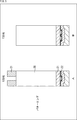
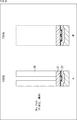
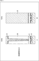
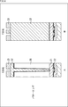
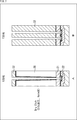
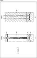
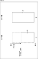
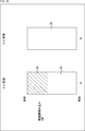
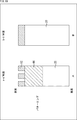
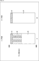
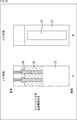
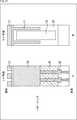
- FIG. 1 It is a top view of the solid-state image sensor which provided the penetration electrode and the trench structure side by side. It is sectional drawing corresponding to FIG. It is a figure which shows the formation method of a trench structure and a penetration electrode. It is a figure which shows the formation method of a trench structure and a penetration electrode. It is a figure which shows the formation method of a trench structure and a penetration electrode. It is a figure which shows the formation method of a trench structure and a penetration electrode. It is a figure which shows the formation method of a trench structure and a penetration electrode. It is a figure which shows the formation method of a trench structure and a penetration electrode. It is a figure which shows the formation method of a trench structure and a penetration electrode. It is a figure which shows the formation method of a trench structure and a penetration electrode. It is a figure which shows the formation method of a trench structure and a penetration electrode.
- FIG. 1 is a plan view of a solid-state imaging device according to an embodiment of the present disclosure.
- 2 is a cross-sectional view corresponding to FIG. 1, in which A in FIG. 2 corresponds to the X direction in the through electrode in FIG. 1, and B in FIG. 2 corresponds to the Y direction in the through electrode in FIG.
- This solid-state imaging device 10 is a so-called back-illuminated CMOS image sensor, and three photoelectric conversion portions (photoelectric conversion films, PDs, etc.) are stacked in the vertical direction for each pixel so as to surround each pixel section 14.
- the trench structure 11 is formed in a lattice shape.
- the trench structure 11 is for preventing color mixture that may occur due to leakage of charges to adjacent pixels.
- a wall made of an insulator (insulating film) such as SiO 2 or SiN extends to the inside of the Si substrate. Is formed.
- an intersection at which straight portions arranged in the vertical and horizontal directions intersect is particularly referred to as a trench structure cross portion 12.
- a through electrode 13 penetrating the Si substrate 20 is formed at a position overlapping the trench structure 11.
- the through electrode 13 is made of a conductive metal such as W, TiN, or Ti, and an insulator made of the same material as that of the trench structure is formed around the through electrode 13.
- FIGS. 3 to 9 show a method for forming the trench structure 11 and the through electrode 13 in the solid-state imaging device 10.
- Each figure A and each figure B correspond to A in FIG. 2 and B in FIG. 2, respectively.
- the through electrode 13 is formed on the rear side (upper side in the figure, light incident side). To do.
- patterning is performed in which a portion other than the position where the trench structure 11 is formed is covered with a resist 31 by lithography.
- a portion of the Si substrate 20 not covered with the resist 31 is processed into a groove shape for the trench structure 11 by dry etching or the like.
- the dry etching at this time is stopped up to the oxide film of STI (Shallow Trench Isolation) 21.
- the oxide film of STI 21 may be processed into a groove shape and dry etching up to the Poly electrode 22 may be performed.
- an insulating film 32 such as SiO 2 or SiN is embedded in the groove formed in the Si substrate 20 in FIG. 4 by a method such as plasma CVD.
- patterning is performed by covering the trench structure 11 with a resist 33 by lithography except for the position where the through electrode 13 is provided.
- the portion of the insulating film 32 and the STI 21 not covered with the resist 33 are processed into a hole shape by dry etching or the like and penetrated to the poly electrode 22.
- the metal 34 having conductivity such as W, TiN, Ti or the like is buried in the holes formed in the insulating film 32 and the STI 21 in FIG.
- the through electrode 13 is formed by removing unnecessary portions of the buried metal 34.
- the through electrode 13 can be simultaneously formed in the trench structure 11 and the overlapping position.
- the color mixture between adjacent pixels can be suppressed by having the trench structure 11.
- the trench structure 11 and the through electrode 13 are overlapped, it is not necessary to provide a dedicated region for the through electrode 13, so that the solid-state imaging device 10 can be miniaturized and the area of the PD in each pixel can be reduced. It is possible to enlarge, and Qs and light receiving sensitivity can be improved.
- FIG. 10 to FIG. 12 show another forming method (second forming method) of the trench structure 11 and the through electrode 13 in the solid-state imaging device 10.
- the layout dimension (width of a line not covered by the register 31) when forming the trench structure 11, the trench structure cross portion 12, and the through electrode 13 is the widest for the through electrode 13, and the next is the trench structure cross.
- the portion 12 is wide, and the trench structure (straight portion) 11 is formed to be the narrowest.
- the through electrode 13 has the deepest depth when the Si substrate 20 is processed into a groove shape or a hole shape.
- the trench structure cross portion 12 is formed deep, and the trench structure (straight portion) 11 is formed shallowest. Depth during processing Through-electrode 13> trench structure cross section 12> trench structure (straight section) 11
- FIG. 13 shows an example of layout dimensions and depths during processing of the trench structure 11, the trench structure cross portion 12, and the through electrode 13. Note that the specific numerical values of the layout dimensions and depths shown in the drawing are merely examples, and vary depending on the overall size of the solid-state imaging device 10 and the aperture ratio of the holes.
- the layout dimensions of the trench structure 11, the trench structure cross portion 12, and the through electrode 13 and the depth during processing are formed according to the above-described magnitude relationship, these can be arranged efficiently or simultaneously. it can.
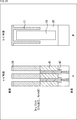
- FIGS. 14A and 14B are diagrams for explaining the third forming method.
- FIG. 14A is a plan view of the solid-state imaging device 10 and
- FIG. 14B is a surface of the Si substrate 20 of the solid-state imaging device 10 (light incident surface).
- FIG. 5B shows the configuration of the back surface (light incident surface) of the Si substrate 20 of the solid-state imaging device 10.
- a DTI (Deep Trench Isolation) 41 is formed on the surface side of the Si substrate 20 as shown in FIG. A Poly electrode 42 is formed.
- a trench structure 11 made of an insulating film 44 and a through electrode 13 made of a metal 43 are formed on the back side of the Si substrate 20, as shown in FIG. C.
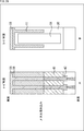
- FIG. 15 is a cross-sectional view corresponding to FIG. 14A.
- FIG. 15A corresponds to a portion where the trench structure 11 and the through electrode 13 overlap each other in the line segment aa ′ of FIG. 15B corresponds to a portion where the trench structure 11 is formed in the line segment bb ′ of FIG. 14A.
- the upper side of the drawing is the back surface (light incident surface) of the solid-state imaging device 10
- the lower side of the drawing is the surface of the solid-state imaging device 10.
- the trench structure 11 is formed of an insulating film 44 formed from the back surface side.
- the through electrode 13 is formed by connecting a poly electrode 42 formed from the front surface side and a metal 43 embedded in the insulating film 44 from the back surface side.
- FIG. 16 to FIG. 30 specifically show the third forming method.
- Each figure A and each figure B correspond to A in FIG. 15 and B in FIG. 15, respectively.
- the upper side of the drawing is the surface of the solid-state imaging device 10
- the lower side of the drawing is the back surface of the solid-state imaging device 10.
- the upper side of the drawing is the back surface of the solid-state image sensor 10
- the lower side of the drawing is the surface of the solid-state image sensor 10.
- DTI 41 is formed on the surface side of the Si substrate 20. Specifically, as shown in FIG. 16, a resist 51 covering the surface side of the Si substrate 20 except for the groove for forming the DTI 41 is patterned by lithography. Subsequently, as shown in FIG. 17, a groove of about 1 ⁇ m is formed from the surface side of the Si substrate 20 by dry etching or the like. Subsequently, as shown in FIG. 18, an insulating film 44 such as an oxide film is buried in the formed trench by CVD (chemical vapor deposition) or the like, and an insulating film 44 whose surface is not required by CMP (chemical mechanical polishing) or the like. The DTI 41 is formed by polishing.
- CVD chemical vapor deposition
- CMP chemical mechanical polishing
- a Poly electrode 42 is formed on the formed DTI 41.
- a resist 52 that covers other than the hole for forming the Poly electrode 42 is patterned by lithography.
- the DTI 41 (insulating film 44) is processed into a hole shape by dry etching or the like.
- a conductive film 53 such as doped poly-Si or metal film is formed by CVD or the like from the surface side of the Si substrate 20, thereby forming the formed holes with the conductive film 53.
- a poly electrode 42 is formed by forming a necessary structure in the transistor region on the surface side of the Si substrate 20.
- a photoelectric conversion unit 54 such as a PD is formed in the Si substrate 20 surrounded by the trench structure 11 as shown in FIG.
- a through electrode 13 is formed by embedding metal from the back side of the Si substrate 20 and connecting it to the poly electrode 42.
- the position (through electrode 13 is formed) The resist 55 is covered by lithography so as to cover the portions other than the portion including the formation position.
- the Si substrate 20 is processed by dry etching or the like to form lattice-shaped grooves. This dry etching is stopped at the previously formed insulating film 44 of the DTI 41. Further, the through electrode groove and the inter-pixel light shielding RDTI groove are formed simultaneously.
- the formed trench is filled with an insulating film 56 such as an oxide film by plasma CVD or the like.
- an insulating film 56 such as an oxide film by plasma CVD or the like.
- the trench structure 11 is formed.
- a resist 57 covering other than the position where the through electrode 13 is formed is patterned by lithography.
- the insulating film 56 (also the trench structure 11) is processed by dry etching or the like, and holes for the through electrode 13 are formed until the poly electrode 42 is reached.
- a hole formed of a metal 58 such as W, TiN, or Ti is buried by sputtering or the like.
- unnecessary metal 58 on the back surface of the Si substrate 20 is removed by CMP or the like, and the through electrode 13 penetrating the Si substrate 20 is completed.
- the color mixture between adjacent pixels can be suppressed by having the trench structure 11.
- the trench structure 11 and the through electrode 13 are overlapped, it is not necessary to provide a dedicated region for the through electrode 13, so that the solid-state imaging device 10 can be miniaturized and the area of the PD in each pixel can be reduced. It is possible to enlarge, and Qs and light receiving sensitivity can be improved.
- FIG. 31 shows an extension example of the trench structure 11.
- the trench structure 11 may be formed to extend deeper. Specifically, when the DTI 41 is formed from the surface side of the Si substrate 20, patterning is performed also on a portion extending the trench structure 11 to form a groove, and the groove is filled with the same insulating film 44 as the DTI 41. Then, it is connected to the trench structure 11 to be formed later. Thereby, it is possible to further suppress color mixing between adjacent pixels.
- FIG. 32 is a diagram illustrating a usage example in which the solid-state imaging device 10 according to the embodiment of the present disclosure is used.
- the solid-state imaging device 10 can be used in various cases for sensing light such as visible light, infrared light, ultraviolet light, and X-ray as follows.
- Devices for taking images for viewing such as digital cameras and mobile devices with camera functions
- Devices used for traffic such as in-vehicle sensors that capture the back, surroundings, and interiors of vehicles, surveillance cameras that monitor traveling vehicles and roads, and ranging sensors that measure distances between vehicles, etc.
- Equipment used for home appliances such as TVs, refrigerators, air conditioners, etc. to take pictures and operate the equipment according to the gestures ⁇ Endoscopes, equipment that performs blood vessel photography by receiving infrared light, etc.
- Equipment used for medical and health care ⁇ Security equipment such as security surveillance cameras and personal authentication cameras ⁇ Skin measuring instrument for photographing skin and scalp photography Such as a microscope to do beauty Equipment used for sports such as action cameras and wearable cameras for sports applications etc.
- Equipment used for agriculture such as cameras for monitoring the condition of fields and crops
- This indication can also take the following composition.
- a trench structure comprising a wall surface of an insulating film formed in the depth direction of the semiconductor substrate and surrounding each pixel section;
- a solid-state imaging device comprising: a penetrating electrode that penetrates the semiconductor substrate and is formed at a position overlapping the trench structure.
- the through electrode connects the photoelectric conversion unit formed on one surface of the semiconductor substrate and an FD formed on the other surface of the semiconductor substrate.
- the photoelectric conversion unit includes a photoelectric conversion film formed on one surface of the semiconductor substrate.
- the solid-state imaging device is A photoelectric conversion unit formed for each pixel section of the semiconductor substrate; A trench structure comprising a wall surface of an insulating film formed in the depth direction of the semiconductor substrate and surrounding each pixel section; An electronic device comprising: a penetrating electrode that penetrates the semiconductor substrate and is formed at a position overlapping the trench structure.
- the layout dimensions of the immediately preceding portion and the cross portion of the trench structure and the through electrode have the following relationship: Through electrode> cross portion of the trench structure> straight portion of the trench structure.
- the immediately preceding portion and the cross portion of the trench structure, and the depth of the through electrode have the following relationship: through electrode> cross portion of the trench structure> straight portion of the trench structure
- a photoelectric conversion unit formed for each pixel section of the semiconductor substrate A trench structure comprising a wall surface of an insulating film formed in the depth direction of the semiconductor substrate and surrounding each pixel section; A through-electrode formed through the semiconductor substrate at a position overlapping with the trench structure;
- the trench structure is composed of a cross portion where the straight portion and the straight portion intersect, In the method of manufacturing a solid-state imaging device, the through electrode is formed at a position overlapping with the linear portion of the trench structure.
- the linear dimension and the cross part of the trench structure, and the layout dimension of the through electrode have the following relationship: Penetration electrode> cross portion of trench structure> straight portion of trench structure.
- the immediately preceding portion and the cross portion of the trench structure, and the depth of the penetration electrode have the following relationship.
- the solid-state imaging device is A photoelectric conversion unit formed for each pixel section of the semiconductor substrate; A trench structure comprising a wall surface of an insulating film formed in the depth direction of the semiconductor substrate and surrounding each pixel section; A through-electrode formed through the semiconductor substrate at a position overlapping with the trench structure; The trench structure is composed of a cross portion where the straight portion and the straight portion intersect, The penetrating electrode is formed at a position overlapping the straight portion of the trench structure.
- a photoelectric conversion unit formed for each pixel section of the semiconductor substrate A trench structure comprising a wall surface of an insulating film formed in the depth direction of the semiconductor substrate and surrounding each pixel section; A through-electrode formed through the semiconductor substrate at a position overlapping with the trench structure; The through electrode is formed by connecting a first conductive portion formed from one surface of the semiconductor substrate and a second conductive portion formed from the other surface of the semiconductor substrate.
- the solid-state imaging device according to (12) or (13), wherein the photoelectric conversion unit includes a photoelectric conversion film formed on one surface of the semiconductor substrate.
- a manufacturing method of a solid-state imaging device comprising a through electrode formed at a position that penetrates the semiconductor substrate and overlaps with the trench structure, Forming a second conductive portion at a position where the through electrode is provided from one surface of the semiconductor substrate;
- the solid-state imaging device is A photoelectric conversion unit formed for each pixel section of the semiconductor substrate; A trench structure comprising a wall surface of an insulating film formed in the depth direction of the semiconductor substrate and surrounding each pixel section; A through-electrode formed through the semiconductor substrate at a position overlapping with the trench structure;
- the penetrating electrode is an electronic device in which a first conductive portion formed from one surface of the semiconductor substrate and a second conductive portion formed from the other surface of the semiconductor substrate are connected.
Landscapes
- Engineering & Computer Science (AREA)
- Multimedia (AREA)
- Signal Processing (AREA)
- Solid State Image Pick-Up Elements (AREA)
- Transforming Light Signals Into Electric Signals (AREA)
Abstract
本開示は、固体撮像素子の各画素区画を囲むトレンチ構造と貫通電極とを効率的に併設することができるようにする固体撮像素子、製造方法、および電子機器に関する。 本開示の第1の側面である固体撮像素子は、半導体基板の画素区画毎に形成されている光電変換部と、前記半導体基板の深さ方向に形成された絶縁膜の壁面から成り、各画素区画を取り囲むトレンチ構造と、前記半導体基板を貫き、前記トレンチ構造と重複する位置に形成された貫通電極とを備える。本開示は、例えば裏面照射型CMOSイメージセンサに適用できる。
Description
本開示は、固体撮像素子、製造方法、および電子機器に関し、特に、画素毎に貫通電極を設ける場合に用いて好適な固体撮像素子、製造方法、および電子機器に関する。
近年、CCDイメージセンサやCMOSイメージセンサに代表される固体撮像素子では、単位面積当たりの画素数の増加に伴って画素サイズが縮小している。このため、各画素に入射するフォトン数が少なくなって感度が低下してしまいS/Nの低下が生じて得る。
また、現在広く用いられている、各画素がR(赤色),G(緑色),B(青色)のいずれかの色のカラーフィルタで覆われている構造の場合、例えば、赤の画素では、緑と青の光がカラーフィルタを透過せず光電変換に用いられないために、感度の面で損失が生じている。また、各画素はR,G,Bのいずれかの色信号しか得られないので、画素間の補間処理を行うことになるが、その際に偽色が生じ得る。
これらの問題を解決する方法として、画素毎に光電変換部を縦方向に3層積層し、各画素で3色の光電変換信号を得ることができるイメージセンサの構造が知られている。具体的には、例えばSi基板上方にGの光に対応する有機光電変換膜を設け、Si基板内にBとRにそれぞれ対応するPD(フォトダイオード)を積層した構造が提案されている(例えば、特許文献1または2を参照)。
上述した構造の場合、Si基板上方の有機光電変換膜からSi基板の反対面側に形成されているFD(フローティグディフュージョン)に電荷を転送する必要がある。そこで、画素毎のSi基板を貫く貫通電極を形成し、有機光電変換膜から貫通電極を介してFDに電荷を転送する構造が提案されている(例えば、特許文献3を参照)。
上述したように、各画素において光電変換部を積層して貫通電極を設ける構造では微細化が困難であった。
また、隣接する画素間での混色を抑止するために各画素の境界に絶縁体を充填した溝(以下、トレンチ構造またはRDTI構造とも称する)を設ける方法が知られているが、上記した貫通電極とトレンチ構造を併設する場合、それらのレイアウトを工夫する必要がある。
本開示はこのような状況に鑑みてなされたものであり、貫通電極とトレンチ構造を効率的に併設できるようにするものである。
本開示の第1の側面である固体撮像素子は、半導体基板の画素区画毎に形成されている光電変換部と、前記半導体基板の深さ方向に形成された絶縁膜の壁面から成り、各画素区画を取り囲むトレンチ構造と、前記半導体基板を貫き、前記トレンチ構造と重複する位置に形成された貫通電極とを備える。
前記貫通電極は、前記半導体基板の一方の面に形成されている前記光電変換部と前記前記半導体基板の他方の面に形成されているFDを接続することができる。
前記光電変換部は、前記半導体基板の一方の面上に形成されている光電変換膜を含むことができる。
前記貫通電極は、前記トレンチ構造を成す絶縁膜に開けられたHoleに導電膜が埋め込まれて形成されているようにすることができる。
本開示の第1の側面である製造方法は、固体撮像素子の製造方法において、半導体基板の各画素区画を取り囲み、且つ、前記半導体基板の深さ方向に溝を形成し、前記溝に絶縁膜を埋め込むことによりトレンチ構造を形成し、前記トレンチ構造の前記絶縁膜にHoleを形成し、前記Holeに導電膜を埋め込むことにより貫通電極を形成する。
本開示の第1の側面である電子機器は、固体撮像素子が搭載された電子機器において、前記固体撮像素子は、半導体基板の画素区画毎に形成されている光電変換部と、前記半導体基板の深さ方向に形成された絶縁膜の壁面から成り、各画素区画を取り囲むトレンチ構造と、前記半導体基板を貫き、前記トレンチ構造と重複する位置に形成された貫通電極とを備える。
本開示の第2の側面である固体撮像素子は、半導体基板の画素区画毎に形成されている光電変換部と、前記半導体基板の深さ方向に形成された絶縁膜の壁面から成り、各画素区画を取り囲むトレンチ構造と、前記半導体基板を貫き、前記トレンチ構造と重複する位置に形成された貫通電極とを備え、前記トレンチ構造は、直線部分と前記直線部分が交差するクロス部分から成り、前記貫通電極は、前記トレンチ構造の前記直線部分と重複する位置に形成されている。
前記トレンチ構造の直前部およびクロス部、並びに前記貫通電極のレイアウト寸法は、以下の関係を有することができる。
貫通電極>トレンチ構造のクロス部>トレンチ構造の直線部
貫通電極>トレンチ構造のクロス部>トレンチ構造の直線部
前記トレンチ構造の直前部およびクロス部、並びに前記貫通電極の深さは、以下の関係を有することができる。
貫通電極>トレンチ構造のクロス部>トレンチ構造の直線部
貫通電極>トレンチ構造のクロス部>トレンチ構造の直線部
本開示の第2の側面である製造方法は、半導体基板の画素区画毎に形成されている光電変換部と、前記半導体基板の深さ方向に形成された絶縁膜の壁面から成り、各画素区画を取り囲むトレンチ構造と、前記半導体基板を貫き、前記トレンチ構造と重複する位置に形成された貫通電極とを備え、前記トレンチ構造は、直線部分と前記直線部分が交差するクロス部分から成り、前記貫通電極は、前記トレンチ構造の前記直線部分と重複する位置に形成されている固体撮像素子の製造方法において、前記トレンチ構造の前記直線部分および前記クロス部分、並びに前記貫通電極のレイアウト寸法は、以下の関係を有し、
貫通電極>トレンチ構造のクロス部>トレンチ構造の直線部
前記トレンチ構造の直前部およびクロス部、並びに前記貫通電極の深さは、以下の関係を有する
貫通電極>トレンチ構造のクロス部>トレンチ構造の直線部。
貫通電極>トレンチ構造のクロス部>トレンチ構造の直線部
前記トレンチ構造の直前部およびクロス部、並びに前記貫通電極の深さは、以下の関係を有する
貫通電極>トレンチ構造のクロス部>トレンチ構造の直線部。
本開示の第2の側面である電子機器は、固体撮像素子が搭載された電子機器において、前記固体撮像素子は、半導体基板の画素区画毎に形成されている光電変換部と、前記半導体基板の深さ方向に形成された絶縁膜の壁面から成り、各画素区画を取り囲むトレンチ構造と、前記半導体基板を貫き、前記トレンチ構造と重複する位置に形成された貫通電極とを備え、前記トレンチ構造は、直線部分と前記直線部分が交差するクロス部分から成り、前記貫通電極は、前記トレンチ構造の前記直線部分と重複する位置に形成されている。
本開示の第3の側面である固定撮像素子は、半導体基板の画素区画毎に形成されている光電変換部と、前記半導体基板の深さ方向に形成された絶縁膜の壁面から成り、各画素区画を取り囲むトレンチ構造と、前記半導体基板を貫き、前記トレンチ構造と重複する位置に形成された貫通電極とを備え、前記貫通電極は、前記半導体基板の一方の面から形成された第1の導電部と、前記半導体基板の他方の面から形成された第2の導電部とが接続されて成る。
前記貫通電極は、前記半導体基板の一方の面に形成されている前記光電変換部と前記前記半導体基板の他方の面に形成されているFDを接続することができる。
前記光電変換部は、前記半導体基板の一方の面上に形成されている光電変換膜を含むことができる。
本開示の第3の側面である製造方法は、半導体基板の画素区画毎に形成されている光電変換部と、前記半導体基板の深さ方向に形成された絶縁膜の壁面から成り、各画素区画を取り囲むトレンチ構造と、前記半導体基板を貫き、前記トレンチ構造と重複する位置に形成された貫通電極とを備える固体撮像素子の製造方法において、前記半導体基板の一方の面から前記貫通電極を設ける位置に第2の導電部を形成し、前記半導体基板の他方の面から半導体基板の各画素区画を取り囲み、且つ、前記半導体基板の深さ方向に溝を形成し、前記溝に絶縁膜を埋め込むことによりトレンチ構造を形成し、前記半導体基板の他方の面から前記トレンチ構造の前記絶縁膜にHoleを形成し、前記Holeに導電膜を埋め込むことにより第2の導電部を形成して前記第1の導電部と接続させることにより前記貫通電極を形成する。
本開示の第3の側面である電子機器は、固体撮像素子が搭載された電子機器において、前記固体撮像素子は、半導体基板の画素区画毎に形成されている光電変換部と、前記半導体基板の深さ方向に形成された絶縁膜の壁面から成り、各画素区画を取り囲むトレンチ構造と、前記半導体基板を貫き、前記トレンチ構造と重複する位置に形成された貫通電極とを備え、前記貫通電極は、前記半導体基板の一方の面から形成された第1の導電部と、前記半導体基板の他方の面から形成された第2の導電部とが接続されて成る。
本開示の第1乃至第3の側面によれば、貫通電極とトレンチ構造が効率的に併設された固体撮像素子を実現できる。
また、本開示の第1乃至第3の側面によれば、隣接画素間での混色が抑止される。
さらに、本開示の第1乃至第3の側面によれば、固体撮像素子の微細化が可能となって光電変換部の面積を拡大でき、受光感度を向上させることができる。
以下、本開示を実施するための最良の形態(以下、実施の形態と称する)について、図面を参照しながら詳細に説明する。
<本開示の実施の形態である固体撮像素子について>
図1は、本開示の実施の形態である固体撮像素子の平面図を示している。図2は、図1に対応する断面図であり、図2のAが図1の貫通電極におけるX方向に対応し、図2のBが図1の貫通電極におけるY方向に対応する。
図1は、本開示の実施の形態である固体撮像素子の平面図を示している。図2は、図1に対応する断面図であり、図2のAが図1の貫通電極におけるX方向に対応し、図2のBが図1の貫通電極におけるY方向に対応する。
この固体撮像素子10は、いわゆる裏面照射型のCMOSイメージセンサであって、画素毎に光電変換部(光電変換膜、PDなど)が縦方向に3層積層され、各画素区画14を取り囲むようにトレンチ構造11が格子状に形成されている。トレンチ構造11は、隣接画素に電荷が漏れ出すことによって生じ得る混色を防止するためのものであり、例えば、SiO2,SiN等の絶縁体(絶縁膜)から成る壁がSi基板の内部にまで形成されている。トレンチ構造11のうち、特に、縦横に配された直線部分が交差する交点をトレンチ構造クロス部12と称する。
さらに、固体撮像素子10には、トレンチ構造11と重なる位置に、Si基板20を貫く貫通電極13が形成されている。貫通電極13は、例えば、W,TiN,Tiなどの導電性メタルから成り、その周囲にはトレンチ構造と同じ材料の絶縁体が形成されている。
<固体撮像素子10におけるトレンチ構造11と貫通電極13の第1の形成方法>
次に、図3乃至図9は、固体撮像素子10におけるトレンチ構造11と貫通電極13の形成方法を示している。なお、各図Aと各図Bは、それぞれ図2のAと図2のBに対応するものである。
始めに、Si基板20の表側(図中の下側)に各種のトランジスタなど必要な構成要素を作り込んだ後、裏面側(図中の上側、光の入射面側)に貫通電極13を形成する。
具体的には、図3に示すように、トレンチ構造11を形成する位置以外をリソグラフィによってレジスト31で覆うパターニングを行う。次に、図4に示すように、レジスト31で覆われていない部分のSi基板20をドライエッチング等でトレンチ構造11のために溝状に加工する。なお、この際のドライエッチングは、STI(Shallow Trench Isolation)21の酸化膜までで止めるようにする。ただし、STI21の酸化膜を溝状に加工し、Poly電極22までドライエッチングを行ってもよい。
続いて、図5に示すように、図4でSi基板20に形成した溝に、例えば、プラズマCVD等の手法でSiO2やSiN等の絶縁膜32を埋め込む。次に、図6に示すように、トレンチ構造11に重なって貫通電極13を設ける位置以外をリソグラフィによってレジスト33で覆うパターニングを行う。続いて、図7に示すように、レジスト33で覆われていない部分の絶縁膜32およびSTI21をドライエッチング等でhole状に加工し、Poly電極22まで貫通させる。
この後、図8に示すように、図7で絶縁膜32およびSTI21に形成したholeに、例えば、スパッタリング等の手法でW,TiN,Ti等の導電性を有するメタル34を埋め込み、さらに、図9に示すように、埋め込んだメタル34の不要な部位を除去することによって、貫通電極13を形成する。
以上の工程により、トレンチ構造11とそれに重なる位置に貫通電極13を同時に形成することができる。
なお、先にトレンチ構造11を形成してから、それに重なる位置に貫通電極13を形成するようにしてもよい。
以上に説明した第1の形成方法による固体撮像素子10によれば、トレンチ構造11を有することにより、隣接画素間での混色を抑止することができる。また、トレンチ構造11と貫通電極13を重ねたことにより、貫通電極13のために専用領域を設ける必要が無くなるので、固体撮像素子10の微細化が可能となり、また、各画素におけるPDの面積を拡大でき、Qsや受光感度を向上させることができる。
<トレンチ構造11、および貫通電極13の他の形成方法(第2の形成方法)>
次に、図10乃至図12は、固体撮像素子10におけるトレンチ構造11と貫通電極13の他の形成方法(第2の形成方法)を示している。
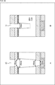
第2の形成方法の場合、トレンチ構造11に重ねて貫通電極13を形成する位置には、トレンチ構造11だけを形成する位置よりも広く、深いエッチングを行う。具体的には、トレンチ構造11、トレンチ構造クロス部12、および貫通電極13を形成する際のレイアウト寸法(レジスタ31により覆わない線の幅)は、貫通電極13が最も広く、次にトレンチ構造クロス部12が広く、トレンチ構造(直線部)11が最も狭くなるように形成する。
レイアウト寸法
貫通電極13 > トレンチ構造クロス部12 > トレンチ構造(直線部)11
レイアウト寸法
貫通電極13 > トレンチ構造クロス部12 > トレンチ構造(直線部)11
また、固体撮像素子10におけるトレンチ構造11、トレンチ構造クロス部12、および貫通電極13を形成する際にSi基板20を溝状またはhole状に加工する際の深さは、貫通電極13が最も深く、次にトレンチ構造クロス部12が深く、トレンチ構造(直線部)11が最も浅くなるように形成する。
加工時の深さ
貫通電極13 > トレンチ構造クロス部12 > トレンチ構造(直線部)11
加工時の深さ
貫通電極13 > トレンチ構造クロス部12 > トレンチ構造(直線部)11
図13は、トレンチ構造11、トレンチ構造クロス部12、および貫通電極13のレイアウト寸法や加工時の深さの一例を示している。なお、図中に記されているレイアウト寸法や深さの具体的数値については一例に過ぎず、固体撮像装置10の全体のサイズやholeの開口率によって変動するものである。
トレンチ構造11、トレンチ構造クロス部12、および貫通電極13のレイアウト寸法と加工時の深さを上述した大小関係で形成すれば、これらを効率的に配置することができ、または同時に形成することができる。
<トレンチ構造11、および貫通電極13のさらに他の形成方法(第3の形成方法)>
次に、固体撮像素子10におけるトレンチ構造11と貫通電極13のさらに他の形成方法(第3の形成方法)について説明する。
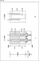
図14は、第3の形成方法を説明するためのものであり、同図Aは固体撮像素子10の平面図、同図Bは固体撮像素子10のSi基板20の表面(光の入射面の反対面)の構成、同図Bは固体撮像素子10のSi基板20の裏面(光の入射面)の構成を示している。
トレンチ構造11と貫通電極13の第3の形成方法では、Si基板20の表面側には、同図Bに示されるように、DTI(Deep Trench Isolation)41が形成され、貫通電極13の位置にPoly電極42が形成される。一方、Si基板20の裏面側には、同図Cに示されるように、絶縁膜44から成るトレンチ構造11と、メタル43から成る貫通電極13が形成される。
図15は、図14のAに対応する断面図であり、図15のAが図14のAの線分a-a’におけるトレンチ構造11と貫通電極13が重なって形成される部位に対応し、図15のBが図14のAの線分b-b’におけるトレンチ構造11が形成される部位に対応する。なお、図15においては、図面の上側が固体撮像素子10の裏面(光の入射面)であり、図面の下側が固体撮像素子10の表面である。
トレンチ構造11は、図15のAおよび図15のBに示されるように、裏面側から形成された絶縁膜44により形成されている。一方、貫通電極13は、図15のAに示されるように、表面側から形成されたPoly電極42と、裏面側から絶縁膜44内に埋め込まれたメタル43が接続されて形成されている。
次に、図16乃至図30は、第3の形成方法を具体的に示している。なお、各図Aと各図Bは、それぞれ図15のAと図15のBに対応するものである。ただし、図16乃至図22においては、図面の上側が固体撮像素子10の表面であり、図面の下側が固体撮像素子10の裏面である。また、図23乃至図30においては、図面の上側が固体撮像素子10の裏面であり、図面の下側が固体撮像素子10の表面である。
はじめに、Si基板20の表面側にDTI41を形成する。具体的には、図16に示されるように、Si基板20の表面側に、DTI41を形成するための溝以外を覆うレジスト51をリソグラフィによってパターニングする。続いて、図17に示されるように、Si基板20の表面側から、ドライエッチングなどにより1μm程度の溝を形成する。続いて、図18に示すように、形成された溝に対し、CVD(chemical vapor deposition)等により酸化膜等の絶縁膜44を埋め込み、CMP(chemical mechanical polishing)などによって表面の不要な絶縁膜44を研磨することにより、DTI41を形成する。
次に、形成したDTI41にPoly電極42を形成する。具体的には、図19に示すように、Poly電極42を形成するためのhole以外を覆うレジスト52をリソグラフィによってパターニングする。続いて、図20に示されるように、ドライエッチングなどにより、DTI41(絶縁膜44)をhole状に加工する。続いて図21に示すように、Si基板20の表面側からCVDなどにより、例えばドープされたPoly Siやメタル膜などの導電膜53を成膜させることにより、形成されたholeを導電膜53で埋め込む。さらに、図22に示すように、Si基板20の表面側のトランジスタ領域に必要な構造を作り込むことにより、Poly電極42を形成する。なお、ここまでに、トレンチ構造11で囲まれるSi基板20の内部には、図22のBに示すように、PD等の光電変換部54が形成されるものとする。
次に、Si基板20の裏面側からメタルを埋め込み、Poly電極42と接続させることによって貫通電極13を形成する。具体的には、図23に示すように、Si基板20の表裏を反転させた後、図24に示すように、Si基板20の裏面側から、トレンチ構造11を形成する位置(貫通電極13を形成する位置も含む)以外を覆うレジスト55をリソグラフィによってパターニングする。続いて、図25に示されるように、ドライエッチング等によってSi基板20を加工して格子状の溝を形成する。このドライエッチングは、先に形成されているDTI41の絶縁膜44で停止される。また、貫通電極用の溝と画素間遮光用のRDTI用の溝は同時に形成する。
続いて、図26に示すように、プラズマCVD等により酸化膜等の絶縁膜56で、形成された溝内を埋め込む。これにより、トレンチ構造11が形成される。続いて、図27に示すように、貫通電極13を形成する位置以外を覆うレジスト57をリソグラフィによってパターニングする。続いて、図28に示されるように、ドライエッチング等によって絶縁膜56(トレンチ構造11でもある)を加工して、Poly電極42に達するまで貫通電極13のためのholeを形成する。この後、図29に示すように、スパッタリング法などによりW,TiN,Tiなどのメタル58で形成されたholeを埋め込む。最後に、図30に示すように、CMPなどによりSi基板20の裏面の不要なメタル58を除去して、Si基板20を貫く貫通電極13が完成される。
以上に説明した第3の形成方法による固体撮像素子10によれば、トレンチ構造11を有することにより、隣接画素間での混色を抑止することができる。また、トレンチ構造11と貫通電極13を重ねたことにより、貫通電極13のために専用領域を設ける必要が無くなるので、固体撮像素子10の微細化が可能となり、また、各画素におけるPDの面積を拡大でき、Qsや受光感度を向上させることができる。
<トレンチ構造11の拡張例>
図31は、トレンチ構造11の拡張例を示している。
図31は、トレンチ構造11の拡張例を示している。
すなわち、図31のBに示すように、トレンチ構造11をより深部に延長して形成してもよい。具体的には、Si基板20の表面側からDTI41を形成する際に、トレンチ構造11を延長する部位についてもパターニングを行って溝を形成し、その溝をDTI41と同じ絶縁膜44で埋め込んでおき、以降に形成するトレンチ構造11と接続させるようにする。これにより、隣接画素間での混色をより抑止することが可能となる。
<固体撮像素子の使用例>
図32は、本開示の実施の形態である固体撮像素子10を使用する使用例を示す図である。
図32は、本開示の実施の形態である固体撮像素子10を使用する使用例を示す図である。
固体撮像素子10は、例えば、以下のように、可視光や、赤外光、紫外光、X線等の光をセンシングする様々なケースに使用することができる。
・デジタルカメラや、カメラ機能付きの携帯機器等の、鑑賞の用に供される画像を撮影する装置
・自動停止等の安全運転や、運転者の状態の認識等のために、自動車の前方や後方、周囲、車内等を撮影する車載用センサ、走行車両や道路を監視する監視カメラ、車両間等の測距を行う測距センサ等の、交通の用に供される装置
・ユーザのジェスチャを撮影して、そのジェスチャに従った機器操作を行うために、TVや、冷蔵庫、エアーコンディショナ等の家電に供される装置
・内視鏡や、赤外光の受光による血管撮影を行う装置等の、医療やヘルスケアの用に供される装置
・防犯用途の監視カメラや、人物認証用途のカメラ等の、セキュリティの用に供される装置
・肌を撮影する肌測定器や、頭皮を撮影するマイクロスコープ等の、美容の用に供される装置
・スポーツ用途等向けのアクションカメラやウェアラブルカメラ等の、スポーツの用に供される装置
・畑や作物の状態を監視するためのカメラ等の、農業の用に供される装置
・自動停止等の安全運転や、運転者の状態の認識等のために、自動車の前方や後方、周囲、車内等を撮影する車載用センサ、走行車両や道路を監視する監視カメラ、車両間等の測距を行う測距センサ等の、交通の用に供される装置
・ユーザのジェスチャを撮影して、そのジェスチャに従った機器操作を行うために、TVや、冷蔵庫、エアーコンディショナ等の家電に供される装置
・内視鏡や、赤外光の受光による血管撮影を行う装置等の、医療やヘルスケアの用に供される装置
・防犯用途の監視カメラや、人物認証用途のカメラ等の、セキュリティの用に供される装置
・肌を撮影する肌測定器や、頭皮を撮影するマイクロスコープ等の、美容の用に供される装置
・スポーツ用途等向けのアクションカメラやウェアラブルカメラ等の、スポーツの用に供される装置
・畑や作物の状態を監視するためのカメラ等の、農業の用に供される装置
なお、本開示の実施の形態は、上述した実施の形態に限定されるものではなく、本開示の要旨を逸脱しない範囲において種々の変更が可能である。
本開示は以下のような構成も取ることができる。
(1)
半導体基板の画素区画毎に形成されている光電変換部と、
前記半導体基板の深さ方向に形成された絶縁膜の壁面から成り、各画素区画を取り囲むトレンチ構造と、
前記半導体基板を貫き、前記トレンチ構造と重複する位置に形成された貫通電極と
を備える固体撮像素子。
(2)
前記貫通電極は、前記半導体基板の一方の面に形成されている前記光電変換部と前記前記半導体基板の他方の面に形成されているFDを接続する
前記(1)に記載の固体撮像素子。
(3)
前記光電変換部は、前記半導体基板の一方の面上に形成されている光電変換膜を含む
前記(1)または(2)に記載の固体撮像素子。
(4)
前記貫通電極は、前記トレンチ構造を成す絶縁膜に開けられたHoleに導電膜が埋め込まれて形成されている
前記(1)から(3)のいずれかに記載の固体撮像素子。
(5)
固体撮像素子の製造方法において、
半導体基板の各画素区画を取り囲み、且つ、前記半導体基板の深さ方向に溝を形成し、前記溝に絶縁膜を埋め込むことによりトレンチ構造を形成し、
前記トレンチ構造の前記絶縁膜にHoleを形成し、前記Holeに導電膜を埋め込むことにより貫通電極を形成する
製造方法。
(6)
固体撮像素子が搭載された電子機器において、
前記固体撮像素子は、
半導体基板の画素区画毎に形成されている光電変換部と、
前記半導体基板の深さ方向に形成された絶縁膜の壁面から成り、各画素区画を取り囲むトレンチ構造と、
前記半導体基板を貫き、前記トレンチ構造と重複する位置に形成された貫通電極と
を備える
電子機器。
(7)
半導体基板の画素区画毎に形成されている光電変換部と、
前記半導体基板の深さ方向に形成された絶縁膜の壁面から成り、各画素区画を取り囲むトレンチ構造と、
前記半導体基板を貫き、前記トレンチ構造と重複する位置に形成された貫通電極と
を備え、
前記トレンチ構造は、直線部分と前記直線部分が交差するクロス部分から成り、
前記貫通電極は、前記トレンチ構造の前記直線部分と重複する位置に形成されている
固体撮像素子。
(8)
前記トレンチ構造の直前部およびクロス部、並びに前記貫通電極のレイアウト寸法は、以下の関係を有する
貫通電極>トレンチ構造のクロス部>トレンチ構造の直線部
前記(7)に記載の固体撮像素子。
(9)
前記トレンチ構造の直前部およびクロス部、並びに前記貫通電極の深さは、以下の関係を有する
貫通電極>トレンチ構造のクロス部>トレンチ構造の直線部
前記(7)または(8)に記載の固体撮像素子。
(10)
半導体基板の画素区画毎に形成されている光電変換部と、
前記半導体基板の深さ方向に形成された絶縁膜の壁面から成り、各画素区画を取り囲むトレンチ構造と、
前記半導体基板を貫き、前記トレンチ構造と重複する位置に形成された貫通電極と
を備え、
前記トレンチ構造は、直線部分と前記直線部分が交差するクロス部分から成り、
前記貫通電極は、前記トレンチ構造の前記直線部分と重複する位置に形成されている固体撮像素子の製造方法において、
前記トレンチ構造の前記直線部分および前記クロス部分、並びに前記貫通電極のレイアウト寸法は、以下の関係を有し、
貫通電極>トレンチ構造のクロス部>トレンチ構造の直線部
前記トレンチ構造の直前部およびクロス部、並びに前記貫通電極の深さは、以下の関係を有する
貫通電極>トレンチ構造のクロス部>トレンチ構造の直線部
製造方法。
(11)
固体撮像素子が搭載された電子機器において、
前記固体撮像素子は、
半導体基板の画素区画毎に形成されている光電変換部と、
前記半導体基板の深さ方向に形成された絶縁膜の壁面から成り、各画素区画を取り囲むトレンチ構造と、
前記半導体基板を貫き、前記トレンチ構造と重複する位置に形成された貫通電極と
を備え、
前記トレンチ構造は、直線部分と前記直線部分が交差するクロス部分から成り、
前記貫通電極は、前記トレンチ構造の前記直線部分と重複する位置に形成されている
電子機器。
(12)
半導体基板の画素区画毎に形成されている光電変換部と、
前記半導体基板の深さ方向に形成された絶縁膜の壁面から成り、各画素区画を取り囲むトレンチ構造と、
前記半導体基板を貫き、前記トレンチ構造と重複する位置に形成された貫通電極と
を備え、
前記貫通電極は、前記半導体基板の一方の面から形成された第1の導電部と、前記半導体基板の他方の面から形成された第2の導電部とが接続されて成る
固体撮像素子。
(13)
前記貫通電極は、前記半導体基板の一方の面に形成されている前記光電変換部と前記前記半導体基板の他方の面に形成されているFDを接続する
前記(12)に記載の固体撮像素子。
(14)
前記光電変換部は、前記半導体基板の一方の面上に形成されている光電変換膜を含む
前記(12)または(13)に記載の固体撮像素子。
(15)
半導体基板の画素区画毎に形成されている光電変換部と、
前記半導体基板の深さ方向に形成された絶縁膜の壁面から成り、各画素区画を取り囲むトレンチ構造と、
前記半導体基板を貫き、前記トレンチ構造と重複する位置に形成された貫通電極と
を備える固体撮像素子の製造方法において、
前記半導体基板の一方の面から前記貫通電極を設ける位置に第2の導電部を形成し、
前記半導体基板の他方の面から半導体基板の各画素区画を取り囲み、且つ、前記半導体基板の深さ方向に溝を形成し、前記溝に絶縁膜を埋め込むことによりトレンチ構造を形成し、
前記半導体基板の他方の面から前記トレンチ構造の前記絶縁膜にHoleを形成し、前記Holeに導電膜を埋め込むことにより第2の導電部を形成して前記第1の導電部と接続させることにより前記貫通電極を形成する
製造方法。
(16)
固体撮像素子が搭載された電子機器において、
前記固体撮像素子は、
半導体基板の画素区画毎に形成されている光電変換部と、
前記半導体基板の深さ方向に形成された絶縁膜の壁面から成り、各画素区画を取り囲むトレンチ構造と、
前記半導体基板を貫き、前記トレンチ構造と重複する位置に形成された貫通電極と
を備え、
前記貫通電極は、前記半導体基板の一方の面から形成された第1の導電部と、前記半導体基板の他方の面から形成された第2の導電部とが接続されて成る
電子機器。
(1)
半導体基板の画素区画毎に形成されている光電変換部と、
前記半導体基板の深さ方向に形成された絶縁膜の壁面から成り、各画素区画を取り囲むトレンチ構造と、
前記半導体基板を貫き、前記トレンチ構造と重複する位置に形成された貫通電極と
を備える固体撮像素子。
(2)
前記貫通電極は、前記半導体基板の一方の面に形成されている前記光電変換部と前記前記半導体基板の他方の面に形成されているFDを接続する
前記(1)に記載の固体撮像素子。
(3)
前記光電変換部は、前記半導体基板の一方の面上に形成されている光電変換膜を含む
前記(1)または(2)に記載の固体撮像素子。
(4)
前記貫通電極は、前記トレンチ構造を成す絶縁膜に開けられたHoleに導電膜が埋め込まれて形成されている
前記(1)から(3)のいずれかに記載の固体撮像素子。
(5)
固体撮像素子の製造方法において、
半導体基板の各画素区画を取り囲み、且つ、前記半導体基板の深さ方向に溝を形成し、前記溝に絶縁膜を埋め込むことによりトレンチ構造を形成し、
前記トレンチ構造の前記絶縁膜にHoleを形成し、前記Holeに導電膜を埋め込むことにより貫通電極を形成する
製造方法。
(6)
固体撮像素子が搭載された電子機器において、
前記固体撮像素子は、
半導体基板の画素区画毎に形成されている光電変換部と、
前記半導体基板の深さ方向に形成された絶縁膜の壁面から成り、各画素区画を取り囲むトレンチ構造と、
前記半導体基板を貫き、前記トレンチ構造と重複する位置に形成された貫通電極と
を備える
電子機器。
(7)
半導体基板の画素区画毎に形成されている光電変換部と、
前記半導体基板の深さ方向に形成された絶縁膜の壁面から成り、各画素区画を取り囲むトレンチ構造と、
前記半導体基板を貫き、前記トレンチ構造と重複する位置に形成された貫通電極と
を備え、
前記トレンチ構造は、直線部分と前記直線部分が交差するクロス部分から成り、
前記貫通電極は、前記トレンチ構造の前記直線部分と重複する位置に形成されている
固体撮像素子。
(8)
前記トレンチ構造の直前部およびクロス部、並びに前記貫通電極のレイアウト寸法は、以下の関係を有する
貫通電極>トレンチ構造のクロス部>トレンチ構造の直線部
前記(7)に記載の固体撮像素子。
(9)
前記トレンチ構造の直前部およびクロス部、並びに前記貫通電極の深さは、以下の関係を有する
貫通電極>トレンチ構造のクロス部>トレンチ構造の直線部
前記(7)または(8)に記載の固体撮像素子。
(10)
半導体基板の画素区画毎に形成されている光電変換部と、
前記半導体基板の深さ方向に形成された絶縁膜の壁面から成り、各画素区画を取り囲むトレンチ構造と、
前記半導体基板を貫き、前記トレンチ構造と重複する位置に形成された貫通電極と
を備え、
前記トレンチ構造は、直線部分と前記直線部分が交差するクロス部分から成り、
前記貫通電極は、前記トレンチ構造の前記直線部分と重複する位置に形成されている固体撮像素子の製造方法において、
前記トレンチ構造の前記直線部分および前記クロス部分、並びに前記貫通電極のレイアウト寸法は、以下の関係を有し、
貫通電極>トレンチ構造のクロス部>トレンチ構造の直線部
前記トレンチ構造の直前部およびクロス部、並びに前記貫通電極の深さは、以下の関係を有する
貫通電極>トレンチ構造のクロス部>トレンチ構造の直線部
製造方法。
(11)
固体撮像素子が搭載された電子機器において、
前記固体撮像素子は、
半導体基板の画素区画毎に形成されている光電変換部と、
前記半導体基板の深さ方向に形成された絶縁膜の壁面から成り、各画素区画を取り囲むトレンチ構造と、
前記半導体基板を貫き、前記トレンチ構造と重複する位置に形成された貫通電極と
を備え、
前記トレンチ構造は、直線部分と前記直線部分が交差するクロス部分から成り、
前記貫通電極は、前記トレンチ構造の前記直線部分と重複する位置に形成されている
電子機器。
(12)
半導体基板の画素区画毎に形成されている光電変換部と、
前記半導体基板の深さ方向に形成された絶縁膜の壁面から成り、各画素区画を取り囲むトレンチ構造と、
前記半導体基板を貫き、前記トレンチ構造と重複する位置に形成された貫通電極と
を備え、
前記貫通電極は、前記半導体基板の一方の面から形成された第1の導電部と、前記半導体基板の他方の面から形成された第2の導電部とが接続されて成る
固体撮像素子。
(13)
前記貫通電極は、前記半導体基板の一方の面に形成されている前記光電変換部と前記前記半導体基板の他方の面に形成されているFDを接続する
前記(12)に記載の固体撮像素子。
(14)
前記光電変換部は、前記半導体基板の一方の面上に形成されている光電変換膜を含む
前記(12)または(13)に記載の固体撮像素子。
(15)
半導体基板の画素区画毎に形成されている光電変換部と、
前記半導体基板の深さ方向に形成された絶縁膜の壁面から成り、各画素区画を取り囲むトレンチ構造と、
前記半導体基板を貫き、前記トレンチ構造と重複する位置に形成された貫通電極と
を備える固体撮像素子の製造方法において、
前記半導体基板の一方の面から前記貫通電極を設ける位置に第2の導電部を形成し、
前記半導体基板の他方の面から半導体基板の各画素区画を取り囲み、且つ、前記半導体基板の深さ方向に溝を形成し、前記溝に絶縁膜を埋め込むことによりトレンチ構造を形成し、
前記半導体基板の他方の面から前記トレンチ構造の前記絶縁膜にHoleを形成し、前記Holeに導電膜を埋め込むことにより第2の導電部を形成して前記第1の導電部と接続させることにより前記貫通電極を形成する
製造方法。
(16)
固体撮像素子が搭載された電子機器において、
前記固体撮像素子は、
半導体基板の画素区画毎に形成されている光電変換部と、
前記半導体基板の深さ方向に形成された絶縁膜の壁面から成り、各画素区画を取り囲むトレンチ構造と、
前記半導体基板を貫き、前記トレンチ構造と重複する位置に形成された貫通電極と
を備え、
前記貫通電極は、前記半導体基板の一方の面から形成された第1の導電部と、前記半導体基板の他方の面から形成された第2の導電部とが接続されて成る
電子機器。
10 固体撮像素子, 11 トレンチ構造, 12 トレンチ構造クロス部, 13 貫通電極, 14 画素区画, 20 Si基板, 21 STI, 22 Poly電極, 32 絶縁膜, 34 メタル, 41 DTI, 42 Poly電極, 44 絶縁膜, 53 導電膜, 54 光電変換部, 56 絶縁膜, 58 メタル
Claims (16)
- 半導体基板の画素区画毎に形成されている光電変換部と、
前記半導体基板の深さ方向に形成された絶縁膜の壁面から成り、各画素区画を取り囲むトレンチ構造と、
前記半導体基板を貫き、前記トレンチ構造と重複する位置に形成された貫通電極と
を備える固体撮像素子。 - 前記貫通電極は、前記半導体基板の一方の面に形成されている前記光電変換部と前記前記半導体基板の他方の面に形成されているFDを接続する
請求項1に記載の固体撮像素子。 - 前記光電変換部は、前記半導体基板の一方の面上に形成されている光電変換膜を含む
請求項2に記載の固体撮像素子。 - 前記貫通電極は、前記トレンチ構造を成す絶縁膜に開けられたHoleに導電膜が埋め込まれて形成されている
請求項1に記載の固体撮像素子。 - 固体撮像素子の製造方法において、
半導体基板の各画素区画を取り囲み、且つ、前記半導体基板の深さ方向に溝を形成し、前記溝に絶縁膜を埋め込むことによりトレンチ構造を形成し、
前記トレンチ構造の前記絶縁膜にHoleを形成し、前記Holeに導電膜を埋め込むことにより貫通電極を形成する
製造方法。 - 固体撮像素子が搭載された電子機器において、
前記固体撮像素子は、
半導体基板の画素区画毎に形成されている光電変換部と、
前記半導体基板の深さ方向に形成された絶縁膜の壁面から成り、各画素区画を取り囲むトレンチ構造と、
前記半導体基板を貫き、前記トレンチ構造と重複する位置に形成された貫通電極と
を備える
電子機器。 - 半導体基板の画素区画毎に形成されている光電変換部と、
前記半導体基板の深さ方向に形成された絶縁膜の壁面から成り、各画素区画を取り囲むトレンチ構造と、
前記半導体基板を貫き、前記トレンチ構造と重複する位置に形成された貫通電極と
を備え、
前記トレンチ構造は、直線部分と前記直線部分が交差するクロス部分から成り、
前記貫通電極は、前記トレンチ構造の前記直線部分と重複する位置に形成されている
固体撮像素子。 - 前記トレンチ構造の直前部およびクロス部、並びに前記貫通電極のレイアウト寸法は、以下の関係を有する
貫通電極>トレンチ構造のクロス部>トレンチ構造の直線部
請求項7に記載の固体撮像素子。 - 前記トレンチ構造の直前部およびクロス部、並びに前記貫通電極の深さは、以下の関係を有する
貫通電極>トレンチ構造のクロス部>トレンチ構造の直線部
請求項7に記載の固体撮像素子。 - 半導体基板の画素区画毎に形成されている光電変換部と、
前記半導体基板の深さ方向に形成された絶縁膜の壁面から成り、各画素区画を取り囲むトレンチ構造と、
前記半導体基板を貫き、前記トレンチ構造と重複する位置に形成された貫通電極と
を備え、
前記トレンチ構造は、直線部分と前記直線部分が交差するクロス部分から成り、
前記貫通電極は、前記トレンチ構造の前記直線部分と重複する位置に形成されている固体撮像素子の製造方法において、
前記トレンチ構造の前記直線部分および前記クロス部分、並びに前記貫通電極のレイアウト寸法は、以下の関係を有し、
貫通電極>トレンチ構造のクロス部>トレンチ構造の直線部
前記トレンチ構造の直前部およびクロス部、並びに前記貫通電極の深さは、以下の関係を有する
貫通電極>トレンチ構造のクロス部>トレンチ構造の直線部
製造方法。 - 固体撮像素子が搭載された電子機器において、
前記固体撮像素子は、
半導体基板の画素区画毎に形成されている光電変換部と、
前記半導体基板の深さ方向に形成された絶縁膜の壁面から成り、各画素区画を取り囲むトレンチ構造と、
前記半導体基板を貫き、前記トレンチ構造と重複する位置に形成された貫通電極と
を備え、
前記トレンチ構造は、直線部分と前記直線部分が交差するクロス部分から成り、
前記貫通電極は、前記トレンチ構造の前記直線部分と重複する位置に形成されている
電子機器。 - 半導体基板の画素区画毎に形成されている光電変換部と、
前記半導体基板の深さ方向に形成された絶縁膜の壁面から成り、各画素区画を取り囲むトレンチ構造と、
前記半導体基板を貫き、前記トレンチ構造と重複する位置に形成された貫通電極と
を備え、
前記貫通電極は、前記半導体基板の一方の面から形成された第1の導電部と、前記半導体基板の他方の面から形成された第2の導電部とが接続されて成る
固体撮像素子。 - 前記貫通電極は、前記半導体基板の一方の面に形成されている前記光電変換部と前記前記半導体基板の他方の面に形成されているFDを接続する
請求項12に記載の固体撮像素子。 - 前記光電変換部は、前記半導体基板の一方の面上に形成されている光電変換膜を含む
請求項13に記載の固体撮像素子。 - 半導体基板の画素区画毎に形成されている光電変換部と、
前記半導体基板の深さ方向に形成された絶縁膜の壁面から成り、各画素区画を取り囲むトレンチ構造と、
前記半導体基板を貫き、前記トレンチ構造と重複する位置に形成された貫通電極と
を備える固体撮像素子の製造方法において、
前記半導体基板の一方の面から前記貫通電極を設ける位置に第2の導電部を形成し、
前記半導体基板の他方の面から半導体基板の各画素区画を取り囲み、且つ、前記半導体基板の深さ方向に溝を形成し、前記溝に絶縁膜を埋め込むことによりトレンチ構造を形成し、
前記半導体基板の他方の面から前記トレンチ構造の前記絶縁膜にHoleを形成し、前記Holeに導電膜を埋め込むことにより第2の導電部を形成して前記第1の導電部と接続させることにより前記貫通電極を形成する
製造方法。 - 固体撮像素子が搭載された電子機器において、
前記固体撮像素子は、
半導体基板の画素区画毎に形成されている光電変換部と、
前記半導体基板の深さ方向に形成された絶縁膜の壁面から成り、各画素区画を取り囲むトレンチ構造と、
前記半導体基板を貫き、前記トレンチ構造と重複する位置に形成された貫通電極と
を備え、
前記貫通電極は、前記半導体基板の一方の面から形成された第1の導電部と、前記半導体基板の他方の面から形成された第2の導電部とが接続されて成る
電子機器。
Priority Applications (3)
| Application Number | Priority Date | Filing Date | Title |
|---|---|---|---|
| CN201680040629.6A CN107851648B (zh) | 2015-07-16 | 2016-07-01 | 固态摄像元件、制造方法和电子装置 |
| US15/742,987 US10529767B2 (en) | 2015-07-16 | 2016-07-01 | Solid state image sensor, fabrication method, and electronic apparatus |
| JP2017528383A JP6800851B2 (ja) | 2015-07-16 | 2016-07-01 | 固体撮像素子、および電子機器 |
Applications Claiming Priority (2)
| Application Number | Priority Date | Filing Date | Title |
|---|---|---|---|
| JP2015-141883 | 2015-07-16 | ||
| JP2015141883 | 2015-07-16 |
Publications (1)
| Publication Number | Publication Date |
|---|---|
| WO2017010311A1 true WO2017010311A1 (ja) | 2017-01-19 |
Family
ID=57757830
Family Applications (1)
| Application Number | Title | Priority Date | Filing Date |
|---|---|---|---|
| PCT/JP2016/069592 Ceased WO2017010311A1 (ja) | 2015-07-16 | 2016-07-01 | 固体撮像素子、製造方法、および電子機器 |
Country Status (4)
| Country | Link |
|---|---|
| US (1) | US10529767B2 (ja) |
| JP (1) | JP6800851B2 (ja) |
| CN (1) | CN107851648B (ja) |
| WO (1) | WO2017010311A1 (ja) |
Cited By (3)
| Publication number | Priority date | Publication date | Assignee | Title |
|---|---|---|---|---|
| JP2020038934A (ja) * | 2018-09-05 | 2020-03-12 | 住友電気工業株式会社 | 半導体受光デバイス |
| JPWO2020158515A1 (ja) * | 2019-01-28 | 2021-12-02 | ソニーグループ株式会社 | 固体撮像素子、電子機器、および固体撮像素子の製造方法 |
| US11257857B2 (en) | 2019-01-09 | 2022-02-22 | Samsung Electronics Co., Ltd. | Image sensors including photoelectric conversion devices, trench, supporter, and isolation layer |
Families Citing this family (2)
| Publication number | Priority date | Publication date | Assignee | Title |
|---|---|---|---|---|
| JP2019176089A (ja) * | 2018-03-29 | 2019-10-10 | ソニーセミコンダクタソリューションズ株式会社 | 固体撮像装置、および電子機器 |
| KR102901404B1 (ko) | 2021-01-22 | 2025-12-18 | 삼성전자주식회사 | 이미지 센서 및 이의 제조 방법 |
Citations (3)
| Publication number | Priority date | Publication date | Assignee | Title |
|---|---|---|---|---|
| JP2003086827A (ja) * | 2001-09-12 | 2003-03-20 | Hamamatsu Photonics Kk | ホトダイオードアレイ、固体撮像装置、及び、放射線検出器 |
| JP2012129551A (ja) * | 2004-08-20 | 2012-07-05 | Zycube:Kk | 三次元積層構造を持つ半導体装置の製造方法 |
| JP2015038931A (ja) * | 2013-08-19 | 2015-02-26 | ソニー株式会社 | 固体撮像素子および電子機器 |
Family Cites Families (20)
| Publication number | Priority date | Publication date | Assignee | Title |
|---|---|---|---|---|
| JPH07245385A (ja) * | 1994-03-08 | 1995-09-19 | Fujitsu Ltd | 受光素子の画素分離方法と受光素子 |
| JP4220808B2 (ja) * | 2003-03-10 | 2009-02-04 | 浜松ホトニクス株式会社 | ホトダイオードアレイおよびその製造方法並びに放射線検出器 |
| JP2006041148A (ja) * | 2004-07-27 | 2006-02-09 | Seiko Epson Corp | 半導体装置の製造方法、半導体装置、及び電子機器 |
| US8120077B2 (en) * | 2004-12-16 | 2012-02-21 | Panasonic Corporation | Solid-state imaging device comprising doped channel stop at isolation regions to suppress noise |
| JP5297135B2 (ja) * | 2008-10-01 | 2013-09-25 | キヤノン株式会社 | 光電変換装置、撮像システム、及び光電変換装置の製造方法 |
| KR101033353B1 (ko) * | 2008-10-14 | 2011-05-09 | 주식회사 동부하이텍 | 이미지센서 및 그 제조방법 |
| JP5564847B2 (ja) * | 2009-07-23 | 2014-08-06 | ソニー株式会社 | 固体撮像装置とその製造方法、及び電子機器 |
| JP2011082253A (ja) * | 2009-10-05 | 2011-04-21 | Sony Corp | 固体撮像装置、および、その製造方法、電子機器 |
| JP5533046B2 (ja) * | 2010-03-05 | 2014-06-25 | ソニー株式会社 | 固体撮像装置、固体撮像装置の製造方法、固体撮像装置の駆動方法、及び電子機器 |
| JP5534927B2 (ja) * | 2010-05-06 | 2014-07-02 | 株式会社東芝 | 固体撮像装置 |
| JP2013125831A (ja) * | 2011-12-14 | 2013-06-24 | Elpida Memory Inc | 半導体装置の製造方法及び半導体装置 |
| JP2013128036A (ja) * | 2011-12-19 | 2013-06-27 | Sony Corp | 撮像素子、撮像装置、並びに、製造装置および方法 |
| JP2013143532A (ja) * | 2012-01-12 | 2013-07-22 | Toshiba Corp | 半導体装置 |
| US20150024369A1 (en) * | 2013-05-07 | 2015-01-22 | Damon Gabriel Brown | Portable message board |
| JP2015153962A (ja) * | 2014-02-18 | 2015-08-24 | ソニー株式会社 | 固体撮像素子および製造方法、並びに電子機器 |
| TWI709340B (zh) * | 2014-11-27 | 2020-11-01 | 日商索尼半導體解決方案公司 | 固體攝像元件及電子機器 |
| CN107431076B (zh) * | 2015-03-09 | 2021-05-14 | 索尼半导体解决方案公司 | 成像元件及其制造方法和电子设备 |
| US10559616B2 (en) * | 2015-07-30 | 2020-02-11 | Sony Semiconductor Solutions Corporation | Solid-state imaging apparatus and electronic device |
| JP6725231B2 (ja) * | 2015-10-06 | 2020-07-15 | ソニーセミコンダクタソリューションズ株式会社 | 固体撮像素子、および電子装置 |
| JP2018037611A (ja) * | 2016-09-02 | 2018-03-08 | ソニーセミコンダクタソリューションズ株式会社 | 受光素子、受光素子の製造方法、撮像素子および電子機器 |
-
2016
- 2016-07-01 WO PCT/JP2016/069592 patent/WO2017010311A1/ja not_active Ceased
- 2016-07-01 JP JP2017528383A patent/JP6800851B2/ja active Active
- 2016-07-01 US US15/742,987 patent/US10529767B2/en active Active
- 2016-07-01 CN CN201680040629.6A patent/CN107851648B/zh active Active
Patent Citations (3)
| Publication number | Priority date | Publication date | Assignee | Title |
|---|---|---|---|---|
| JP2003086827A (ja) * | 2001-09-12 | 2003-03-20 | Hamamatsu Photonics Kk | ホトダイオードアレイ、固体撮像装置、及び、放射線検出器 |
| JP2012129551A (ja) * | 2004-08-20 | 2012-07-05 | Zycube:Kk | 三次元積層構造を持つ半導体装置の製造方法 |
| JP2015038931A (ja) * | 2013-08-19 | 2015-02-26 | ソニー株式会社 | 固体撮像素子および電子機器 |
Cited By (6)
| Publication number | Priority date | Publication date | Assignee | Title |
|---|---|---|---|---|
| JP2020038934A (ja) * | 2018-09-05 | 2020-03-12 | 住友電気工業株式会社 | 半導体受光デバイス |
| US11257857B2 (en) | 2019-01-09 | 2022-02-22 | Samsung Electronics Co., Ltd. | Image sensors including photoelectric conversion devices, trench, supporter, and isolation layer |
| JPWO2020158515A1 (ja) * | 2019-01-28 | 2021-12-02 | ソニーグループ株式会社 | 固体撮像素子、電子機器、および固体撮像素子の製造方法 |
| US20220085110A1 (en) * | 2019-01-28 | 2022-03-17 | Sony Group Corporation | Solid-state imaging element, electronic device, and manufacturing method of solid-state imaging element |
| JP7530835B2 (ja) | 2019-01-28 | 2024-08-08 | ソニーグループ株式会社 | 固体撮像素子、電子機器、および固体撮像素子の製造方法 |
| US12120897B2 (en) * | 2019-01-28 | 2024-10-15 | Sony Group Corporation | Solid-state imaging element, electronic device, and manufacturing method of solid-state imaging element |
Also Published As
| Publication number | Publication date |
|---|---|
| JP6800851B2 (ja) | 2020-12-16 |
| US10529767B2 (en) | 2020-01-07 |
| JPWO2017010311A1 (ja) | 2018-04-26 |
| CN107851648B (zh) | 2022-08-16 |
| CN107851648A (zh) | 2018-03-27 |
| US20190088696A1 (en) | 2019-03-21 |
Similar Documents
| Publication | Publication Date | Title |
|---|---|---|
| TWI735428B (zh) | 攝像元件及其製造方法、以及電子機器 | |
| JP6725231B2 (ja) | 固体撮像素子、および電子装置 | |
| US20200350352A1 (en) | Solid-state imaging device, manufacturing method thereof, and electronic device | |
| CN109863600B (zh) | 成像器件、成像装置以及电子设备 | |
| JP6800851B2 (ja) | 固体撮像素子、および電子機器 | |
| WO2017138370A1 (ja) | 固体撮像素子およびその製造方法、並びに電子機器 | |
| WO2018198814A1 (ja) | 半導体デバイス、製造方法、撮像素子、および電子機器 | |
| WO2016152577A1 (ja) | 固体撮像装置および電子機器 | |
| JP7479801B2 (ja) | 撮像素子、製造方法、および電子機器 | |
| WO2017145815A1 (ja) | 撮像装置 | |
| WO2016052249A1 (ja) | 固体撮像素子および製造方法、並びに電子機器 | |
| WO2016098696A1 (ja) | 固体撮像素子、および電子装置 | |
| WO2017086180A1 (ja) | 固体撮像素子、製造方法、および電子機器 | |
| US20240297192A1 (en) | Solid-state image capturing device and manufacturing method, as well as electronic device | |
| US9215361B2 (en) | Array cameras with light barriers | |
| WO2017018216A1 (ja) | 固体撮像装置及びその製造方法、並びに電子機器 | |
| CN107431078B (zh) | 固体摄像元件和电子设备 | |
| WO2017119317A1 (ja) | 固体撮像素子および製造方法、並びに電子機器 | |
| JP7022174B2 (ja) | 固体撮像素子、および電子装置 | |
| TWI624042B (zh) | 具有多步蝕刻之光通道 | |
| JP2016131203A (ja) | 固体撮像素子、製造方法、および電子装置 |
Legal Events
| Date | Code | Title | Description |
|---|---|---|---|
| 121 | Ep: the epo has been informed by wipo that ep was designated in this application |
Ref document number: 16824291 Country of ref document: EP Kind code of ref document: A1 |
|
| ENP | Entry into the national phase |
Ref document number: 2017528383 Country of ref document: JP Kind code of ref document: A |
|
| NENP | Non-entry into the national phase |
Ref country code: DE |
|
| 122 | Ep: pct application non-entry in european phase |
Ref document number: 16824291 Country of ref document: EP Kind code of ref document: A1 |