WO2017006839A1 - Cellule solaire pérovskite - Google Patents
Cellule solaire pérovskite Download PDFInfo
- Publication number
- WO2017006839A1 WO2017006839A1 PCT/JP2016/069516 JP2016069516W WO2017006839A1 WO 2017006839 A1 WO2017006839 A1 WO 2017006839A1 JP 2016069516 W JP2016069516 W JP 2016069516W WO 2017006839 A1 WO2017006839 A1 WO 2017006839A1
- Authority
- WO
- WIPO (PCT)
- Prior art keywords
- solar cell
- titanium
- oxide
- layer
- perovskite
- Prior art date
Links
- 239000010936 titanium Substances 0.000 claims abstract description 99
- 229910052719 titanium Inorganic materials 0.000 claims abstract description 99
- RTAQQCXQSZGOHL-UHFFFAOYSA-N Titanium Chemical compound [Ti] RTAQQCXQSZGOHL-UHFFFAOYSA-N 0.000 claims abstract description 95
- 239000000463 material Substances 0.000 claims abstract description 94
- 230000005525 hole transport Effects 0.000 claims abstract description 59
- 239000002184 metal Substances 0.000 claims abstract description 29
- 229910052751 metal Inorganic materials 0.000 claims abstract description 28
- 229910001069 Ti alloy Inorganic materials 0.000 claims abstract description 24
- 238000004519 manufacturing process Methods 0.000 claims abstract description 21
- 238000004381 surface treatment Methods 0.000 claims abstract description 15
- 239000004065 semiconductor Substances 0.000 claims abstract description 13
- 230000000903 blocking effect Effects 0.000 claims description 51
- GWEVSGVZZGPLCZ-UHFFFAOYSA-N Titan oxide Chemical compound O=[Ti]=O GWEVSGVZZGPLCZ-UHFFFAOYSA-N 0.000 claims description 42
- OGIDPMRJRNCKJF-UHFFFAOYSA-N titanium oxide Inorganic materials [Ti]=O OGIDPMRJRNCKJF-UHFFFAOYSA-N 0.000 claims description 40
- 229910044991 metal oxide Inorganic materials 0.000 claims description 35
- 150000004706 metal oxides Chemical class 0.000 claims description 35
- 239000010408 film Substances 0.000 claims description 28
- 229910000476 molybdenum oxide Inorganic materials 0.000 claims description 23
- PQQKPALAQIIWST-UHFFFAOYSA-N oxomolybdenum Chemical compound [Mo]=O PQQKPALAQIIWST-UHFFFAOYSA-N 0.000 claims description 22
- 238000000034 method Methods 0.000 claims description 21
- XDXWNHPWWKGTKO-UHFFFAOYSA-N 207739-72-8 Chemical class C1=CC(OC)=CC=C1N(C=1C=C2C3(C4=CC(=CC=C4C2=CC=1)N(C=1C=CC(OC)=CC=1)C=1C=CC(OC)=CC=1)C1=CC(=CC=C1C1=CC=C(C=C13)N(C=1C=CC(OC)=CC=1)C=1C=CC(OC)=CC=1)N(C=1C=CC(OC)=CC=1)C=1C=CC(OC)=CC=1)C1=CC=C(OC)C=C1 XDXWNHPWWKGTKO-UHFFFAOYSA-N 0.000 claims description 18
- 238000010438 heat treatment Methods 0.000 claims description 15
- 230000003647 oxidation Effects 0.000 claims description 14
- 238000007254 oxidation reaction Methods 0.000 claims description 14
- XLOMVQKBTHCTTD-UHFFFAOYSA-N Zinc monoxide Chemical compound [Zn]=O XLOMVQKBTHCTTD-UHFFFAOYSA-N 0.000 claims description 13
- 229910052794 bromium Inorganic materials 0.000 claims description 13
- 229910052801 chlorine Inorganic materials 0.000 claims description 13
- 229910052740 iodine Inorganic materials 0.000 claims description 13
- -1 titanium alkoxide compound Chemical class 0.000 claims description 13
- QVGXLLKOCUKJST-UHFFFAOYSA-N atomic oxygen Chemical compound [O] QVGXLLKOCUKJST-UHFFFAOYSA-N 0.000 claims description 12
- 229910052736 halogen Inorganic materials 0.000 claims description 12
- 150000002367 halogens Chemical class 0.000 claims description 12
- 229910052760 oxygen Inorganic materials 0.000 claims description 12
- 239000001301 oxygen Substances 0.000 claims description 12
- OKTJSMMVPCPJKN-UHFFFAOYSA-N Carbon Chemical class [C] OKTJSMMVPCPJKN-UHFFFAOYSA-N 0.000 claims description 11
- 229910052709 silver Inorganic materials 0.000 claims description 11
- 239000004332 silver Substances 0.000 claims description 11
- 125000000217 alkyl group Chemical group 0.000 claims description 10
- TWNQGVIAIRXVLR-UHFFFAOYSA-N oxo(oxoalumanyloxy)alumane Chemical compound O=[Al]O[Al]=O TWNQGVIAIRXVLR-UHFFFAOYSA-N 0.000 claims description 9
- RVTZCBVAJQQJTK-UHFFFAOYSA-N oxygen(2-);zirconium(4+) Chemical compound [O-2].[O-2].[Zr+4] RVTZCBVAJQQJTK-UHFFFAOYSA-N 0.000 claims description 9
- 229910001928 zirconium oxide Inorganic materials 0.000 claims description 9
- 238000003860 storage Methods 0.000 claims description 8
- 238000002048 anodisation reaction Methods 0.000 claims description 6
- XOLBLPGZBRYERU-UHFFFAOYSA-N tin dioxide Chemical compound O=[Sn]=O XOLBLPGZBRYERU-UHFFFAOYSA-N 0.000 claims description 6
- 229910001887 tin oxide Inorganic materials 0.000 claims description 6
- 239000011787 zinc oxide Substances 0.000 claims description 6
- XMWRBQBLMFGWIX-UHFFFAOYSA-N C60 fullerene Chemical class C12=C3C(C4=C56)=C7C8=C5C5=C9C%10=C6C6=C4C1=C1C4=C6C6=C%10C%10=C9C9=C%11C5=C8C5=C8C7=C3C3=C7C2=C1C1=C2C4=C6C4=C%10C6=C9C9=C%11C5=C5C8=C3C3=C7C1=C1C2=C4C6=C2C9=C5C3=C12 XMWRBQBLMFGWIX-UHFFFAOYSA-N 0.000 claims description 5
- FJDQFPXHSGXQBY-UHFFFAOYSA-L caesium carbonate Chemical compound [Cs+].[Cs+].[O-]C([O-])=O FJDQFPXHSGXQBY-UHFFFAOYSA-L 0.000 claims description 5
- 229910000024 caesium carbonate Inorganic materials 0.000 claims description 5
- PCHJSUWPFVWCPO-UHFFFAOYSA-N gold Chemical compound [Au] PCHJSUWPFVWCPO-UHFFFAOYSA-N 0.000 claims description 5
- 229910052737 gold Inorganic materials 0.000 claims description 5
- 239000010931 gold Substances 0.000 claims description 5
- PQXKHYXIUOZZFA-UHFFFAOYSA-M lithium fluoride Chemical compound [Li+].[F-] PQXKHYXIUOZZFA-UHFFFAOYSA-M 0.000 claims description 5
- 229910000484 niobium oxide Inorganic materials 0.000 claims description 5
- URLJKFSTXLNXLG-UHFFFAOYSA-N niobium(5+);oxygen(2-) Chemical compound [O-2].[O-2].[O-2].[O-2].[O-2].[Nb+5].[Nb+5] URLJKFSTXLNXLG-UHFFFAOYSA-N 0.000 claims description 5
- 229920000144 PEDOT:PSS Polymers 0.000 claims description 4
- 229920001940 conductive polymer Polymers 0.000 claims description 4
- 230000007062 hydrolysis Effects 0.000 claims description 4
- 238000006460 hydrolysis reaction Methods 0.000 claims description 4
- 239000005078 molybdenum compound Substances 0.000 claims description 4
- 150000002752 molybdenum compounds Chemical class 0.000 claims description 4
- 125000002080 perylenyl group Chemical group C1(=CC=C2C=CC=C3C4=CC=CC5=CC=CC(C1=C23)=C45)* 0.000 claims description 4
- 239000002243 precursor Substances 0.000 claims description 4
- 239000010409 thin film Substances 0.000 claims description 4
- XJDNKRIXUMDJCW-UHFFFAOYSA-J titanium tetrachloride Chemical compound Cl[Ti](Cl)(Cl)Cl XJDNKRIXUMDJCW-UHFFFAOYSA-J 0.000 claims description 4
- 150000003682 vanadium compounds Chemical class 0.000 claims description 4
- BQCADISMDOOEFD-UHFFFAOYSA-N Silver Chemical compound [Ag] BQCADISMDOOEFD-UHFFFAOYSA-N 0.000 claims description 3
- HCHKCACWOHOZIP-UHFFFAOYSA-N Zinc Chemical compound [Zn] HCHKCACWOHOZIP-UHFFFAOYSA-N 0.000 claims description 3
- XHCLAFWTIXFWPH-UHFFFAOYSA-N [O-2].[O-2].[O-2].[O-2].[O-2].[V+5].[V+5] Chemical compound [O-2].[O-2].[O-2].[O-2].[O-2].[V+5].[V+5] XHCLAFWTIXFWPH-UHFFFAOYSA-N 0.000 claims description 3
- 229910052782 aluminium Inorganic materials 0.000 claims description 3
- XAGFODPZIPBFFR-UHFFFAOYSA-N aluminium Chemical compound [Al] XAGFODPZIPBFFR-UHFFFAOYSA-N 0.000 claims description 3
- 239000002041 carbon nanotube Substances 0.000 claims description 3
- 229910021393 carbon nanotube Inorganic materials 0.000 claims description 3
- 150000001869 cobalt compounds Chemical class 0.000 claims description 3
- GBRBMTNGQBKBQE-UHFFFAOYSA-L copper;diiodide Chemical compound I[Cu]I GBRBMTNGQBKBQE-UHFFFAOYSA-L 0.000 claims description 3
- BQVVSSAWECGTRN-UHFFFAOYSA-L copper;dithiocyanate Chemical compound [Cu+2].[S-]C#N.[S-]C#N BQVVSSAWECGTRN-UHFFFAOYSA-L 0.000 claims description 3
- 229910021389 graphene Inorganic materials 0.000 claims description 3
- 229910003437 indium oxide Inorganic materials 0.000 claims description 3
- PJXISJQVUVHSOJ-UHFFFAOYSA-N indium(iii) oxide Chemical compound [O-2].[O-2].[O-2].[In+3].[In+3] PJXISJQVUVHSOJ-UHFFFAOYSA-N 0.000 claims description 3
- 229910017053 inorganic salt Inorganic materials 0.000 claims description 3
- 150000002642 lithium compounds Chemical class 0.000 claims description 3
- ORUIBWPALBXDOA-UHFFFAOYSA-L magnesium fluoride Chemical compound [F-].[F-].[Mg+2] ORUIBWPALBXDOA-UHFFFAOYSA-L 0.000 claims description 3
- 239000002070 nanowire Substances 0.000 claims description 3
- 229920000327 poly(triphenylamine) polymer Polymers 0.000 claims description 3
- 229920000767 polyaniline Polymers 0.000 claims description 3
- 229920000123 polythiophene Polymers 0.000 claims description 3
- 229910001935 vanadium oxide Inorganic materials 0.000 claims description 3
- 229910052725 zinc Inorganic materials 0.000 claims description 3
- 239000011701 zinc Substances 0.000 claims description 3
- YVTHLONGBIQYBO-UHFFFAOYSA-N zinc indium(3+) oxygen(2-) Chemical compound [O--].[Zn++].[In+3] YVTHLONGBIQYBO-UHFFFAOYSA-N 0.000 claims description 3
- 229910001635 magnesium fluoride Inorganic materials 0.000 claims description 2
- 239000008151 electrolyte solution Substances 0.000 abstract description 15
- 230000003287 optical effect Effects 0.000 abstract description 10
- XUIMIQQOPSSXEZ-UHFFFAOYSA-N Silicon Chemical compound [Si] XUIMIQQOPSSXEZ-UHFFFAOYSA-N 0.000 abstract description 4
- 229910052710 silicon Inorganic materials 0.000 abstract description 4
- 239000010703 silicon Substances 0.000 abstract description 4
- 230000001235 sensitizing effect Effects 0.000 abstract description 2
- 230000015556 catabolic process Effects 0.000 abstract 1
- 238000006731 degradation reaction Methods 0.000 abstract 1
- LFQSCWFLJHTTHZ-UHFFFAOYSA-N Ethanol Chemical compound CCO LFQSCWFLJHTTHZ-UHFFFAOYSA-N 0.000 description 77
- 239000000243 solution Substances 0.000 description 55
- ZMXDDKWLCZADIW-UHFFFAOYSA-N N,N-Dimethylformamide Chemical compound CN(C)C=O ZMXDDKWLCZADIW-UHFFFAOYSA-N 0.000 description 48
- CSCPPACGZOOCGX-UHFFFAOYSA-N Acetone Chemical compound CC(C)=O CSCPPACGZOOCGX-UHFFFAOYSA-N 0.000 description 34
- WEVYAHXRMPXWCK-UHFFFAOYSA-N Acetonitrile Chemical compound CC#N WEVYAHXRMPXWCK-UHFFFAOYSA-N 0.000 description 30
- RTZKZFJDLAIYFH-UHFFFAOYSA-N Diethyl ether Chemical compound CCOCC RTZKZFJDLAIYFH-UHFFFAOYSA-N 0.000 description 30
- OKKJLVBELUTLKV-UHFFFAOYSA-N Methanol Chemical compound OC OKKJLVBELUTLKV-UHFFFAOYSA-N 0.000 description 30
- MVPPADPHJFYWMZ-UHFFFAOYSA-N chlorobenzene Chemical compound ClC1=CC=CC=C1 MVPPADPHJFYWMZ-UHFFFAOYSA-N 0.000 description 30
- 238000006243 chemical reaction Methods 0.000 description 25
- 238000002360 preparation method Methods 0.000 description 24
- 239000000126 substance Substances 0.000 description 24
- 238000007740 vapor deposition Methods 0.000 description 18
- IJGRMHOSHXDMSA-UHFFFAOYSA-N Atomic nitrogen Chemical compound N#N IJGRMHOSHXDMSA-UHFFFAOYSA-N 0.000 description 16
- BAVYZALUXZFZLV-UHFFFAOYSA-N Methylamine Chemical compound NC BAVYZALUXZFZLV-UHFFFAOYSA-N 0.000 description 16
- 239000007864 aqueous solution Substances 0.000 description 16
- 229910052757 nitrogen Inorganic materials 0.000 description 16
- 239000002904 solvent Substances 0.000 description 16
- KFZMGEQAYNKOFK-UHFFFAOYSA-N Isopropanol Chemical compound CC(C)O KFZMGEQAYNKOFK-UHFFFAOYSA-N 0.000 description 14
- NBIIXXVUZAFLBC-UHFFFAOYSA-N Phosphoric acid Chemical compound OP(O)(O)=O NBIIXXVUZAFLBC-UHFFFAOYSA-N 0.000 description 12
- 239000011248 coating agent Substances 0.000 description 11
- 238000000576 coating method Methods 0.000 description 11
- 239000002253 acid Substances 0.000 description 10
- 239000000758 substrate Substances 0.000 description 10
- WHXSMMKQMYFTQS-UHFFFAOYSA-N Lithium Chemical compound [Li] WHXSMMKQMYFTQS-UHFFFAOYSA-N 0.000 description 9
- XMBWDFGMSWQBCA-UHFFFAOYSA-N hydrogen iodide Chemical compound I XMBWDFGMSWQBCA-UHFFFAOYSA-N 0.000 description 9
- 229910052744 lithium Inorganic materials 0.000 description 9
- UUIMDJFBHNDZOW-UHFFFAOYSA-N 2-tert-butylpyridine Chemical compound CC(C)(C)C1=CC=CC=N1 UUIMDJFBHNDZOW-UHFFFAOYSA-N 0.000 description 8
- CBENFWSGALASAD-UHFFFAOYSA-N Ozone Chemical compound [O-][O+]=O CBENFWSGALASAD-UHFFFAOYSA-N 0.000 description 8
- 150000001875 compounds Chemical class 0.000 description 8
- 238000011156 evaluation Methods 0.000 description 8
- 229910000043 hydrogen iodide Inorganic materials 0.000 description 8
- 150000007522 mineralic acids Chemical class 0.000 description 8
- 238000001953 recrystallisation Methods 0.000 description 8
- 239000000654 additive Substances 0.000 description 7
- 238000000151 deposition Methods 0.000 description 7
- 238000004528 spin coating Methods 0.000 description 7
- 238000009281 ultraviolet germicidal irradiation Methods 0.000 description 7
- XEKOWRVHYACXOJ-UHFFFAOYSA-N Ethyl acetate Chemical compound CCOC(C)=O XEKOWRVHYACXOJ-UHFFFAOYSA-N 0.000 description 6
- 229910000147 aluminium phosphate Inorganic materials 0.000 description 6
- 238000003618 dip coating Methods 0.000 description 6
- 230000002542 deteriorative effect Effects 0.000 description 5
- 239000003792 electrolyte Substances 0.000 description 5
- LLWRXQXPJMPHLR-UHFFFAOYSA-N methylazanium;iodide Chemical compound [I-].[NH3+]C LLWRXQXPJMPHLR-UHFFFAOYSA-N 0.000 description 5
- 238000000926 separation method Methods 0.000 description 5
- HEDRZPFGACZZDS-UHFFFAOYSA-N Chloroform Chemical compound ClC(Cl)Cl HEDRZPFGACZZDS-UHFFFAOYSA-N 0.000 description 4
- 150000007513 acids Chemical class 0.000 description 4
- INQOMBQAUSQDDS-UHFFFAOYSA-N iodomethane Chemical compound IC INQOMBQAUSQDDS-UHFFFAOYSA-N 0.000 description 4
- TZIHFWKZFHZASV-UHFFFAOYSA-N methyl formate Chemical compound COC=O TZIHFWKZFHZASV-UHFFFAOYSA-N 0.000 description 4
- 150000007524 organic acids Chemical class 0.000 description 4
- 150000003839 salts Chemical class 0.000 description 4
- QTBSBXVTEAMEQO-UHFFFAOYSA-N Acetic acid Chemical compound CC(O)=O QTBSBXVTEAMEQO-UHFFFAOYSA-N 0.000 description 3
- UFHFLCQGNIYNRP-UHFFFAOYSA-N Hydrogen Chemical compound [H][H] UFHFLCQGNIYNRP-UHFFFAOYSA-N 0.000 description 3
- 229910019142 PO4 Inorganic materials 0.000 description 3
- KWYUFKZDYYNOTN-UHFFFAOYSA-M Potassium hydroxide Chemical compound [OH-].[K+] KWYUFKZDYYNOTN-UHFFFAOYSA-M 0.000 description 3
- YXFVVABEGXRONW-UHFFFAOYSA-N Toluene Chemical compound CC1=CC=CC=C1 YXFVVABEGXRONW-UHFFFAOYSA-N 0.000 description 3
- 239000000956 alloy Substances 0.000 description 3
- 238000005530 etching Methods 0.000 description 3
- 229910052739 hydrogen Inorganic materials 0.000 description 3
- 239000001257 hydrogen Substances 0.000 description 3
- 235000005985 organic acids Nutrition 0.000 description 3
- 239000010452 phosphate Substances 0.000 description 3
- NBIIXXVUZAFLBC-UHFFFAOYSA-K phosphate Chemical compound [O-]P([O-])([O-])=O NBIIXXVUZAFLBC-UHFFFAOYSA-K 0.000 description 3
- 238000005498 polishing Methods 0.000 description 3
- 239000007921 spray Substances 0.000 description 3
- 238000005507 spraying Methods 0.000 description 3
- XLYOFNOQVPJJNP-UHFFFAOYSA-N water Substances O XLYOFNOQVPJJNP-UHFFFAOYSA-N 0.000 description 3
- WSLDOOZREJYCGB-UHFFFAOYSA-N 1,2-Dichloroethane Chemical compound ClCCCl WSLDOOZREJYCGB-UHFFFAOYSA-N 0.000 description 2
- ZAFNJMIOTHYJRJ-UHFFFAOYSA-N Diisopropyl ether Chemical compound CC(C)OC(C)C ZAFNJMIOTHYJRJ-UHFFFAOYSA-N 0.000 description 2
- IAZDPXIOMUYVGZ-UHFFFAOYSA-N Dimethylsulphoxide Chemical compound CS(C)=O IAZDPXIOMUYVGZ-UHFFFAOYSA-N 0.000 description 2
- CSNNHWWHGAXBCP-UHFFFAOYSA-L Magnesium sulfate Chemical compound [Mg+2].[O-][S+2]([O-])([O-])[O-] CSNNHWWHGAXBCP-UHFFFAOYSA-L 0.000 description 2
- UIIMBOGNXHQVGW-UHFFFAOYSA-M Sodium bicarbonate Chemical compound [Na+].OC([O-])=O UIIMBOGNXHQVGW-UHFFFAOYSA-M 0.000 description 2
- QAOWNCQODCNURD-UHFFFAOYSA-N Sulfuric acid Chemical compound OS(O)(=O)=O QAOWNCQODCNURD-UHFFFAOYSA-N 0.000 description 2
- WNLRTRBMVRJNCN-UHFFFAOYSA-N adipic acid Chemical compound OC(=O)CCCCC(O)=O WNLRTRBMVRJNCN-UHFFFAOYSA-N 0.000 description 2
- 150000001298 alcohols Chemical class 0.000 description 2
- 238000007743 anodising Methods 0.000 description 2
- ZCCIPPOKBCJFDN-UHFFFAOYSA-N calcium nitrate Chemical compound [Ca+2].[O-][N+]([O-])=O.[O-][N+]([O-])=O ZCCIPPOKBCJFDN-UHFFFAOYSA-N 0.000 description 2
- 239000013078 crystal Substances 0.000 description 2
- 230000006866 deterioration Effects 0.000 description 2
- YADSGOSSYOOKMP-UHFFFAOYSA-N dioxolead Chemical compound O=[Pb]=O YADSGOSSYOOKMP-UHFFFAOYSA-N 0.000 description 2
- 239000000975 dye Substances 0.000 description 2
- 150000002148 esters Chemical class 0.000 description 2
- 150000002170 ethers Chemical class 0.000 description 2
- 238000001704 evaporation Methods 0.000 description 2
- 239000011521 glass Substances 0.000 description 2
- 150000002576 ketones Chemical class 0.000 description 2
- JVTAAEKCZFNVCJ-UHFFFAOYSA-N lactic acid Chemical compound CC(O)C(O)=O JVTAAEKCZFNVCJ-UHFFFAOYSA-N 0.000 description 2
- YIXJRHPUWRPCBB-UHFFFAOYSA-N magnesium nitrate Chemical compound [Mg+2].[O-][N+]([O-])=O.[O-][N+]([O-])=O YIXJRHPUWRPCBB-UHFFFAOYSA-N 0.000 description 2
- 238000002156 mixing Methods 0.000 description 2
- 150000002825 nitriles Chemical class 0.000 description 2
- 229920003023 plastic Polymers 0.000 description 2
- 229920003207 poly(ethylene-2,6-naphthalate) Polymers 0.000 description 2
- 229920003229 poly(methyl methacrylate) Polymers 0.000 description 2
- 239000011112 polyethylene naphthalate Substances 0.000 description 2
- 229920000139 polyethylene terephthalate Polymers 0.000 description 2
- 239000005020 polyethylene terephthalate Substances 0.000 description 2
- 239000004926 polymethyl methacrylate Substances 0.000 description 2
- FGIUAXJPYTZDNR-UHFFFAOYSA-N potassium nitrate Chemical compound [K+].[O-][N+]([O-])=O FGIUAXJPYTZDNR-UHFFFAOYSA-N 0.000 description 2
- 239000000843 powder Substances 0.000 description 2
- 238000010248 power generation Methods 0.000 description 2
- FVSKHRXBFJPNKK-UHFFFAOYSA-N propionitrile Chemical compound CCC#N FVSKHRXBFJPNKK-UHFFFAOYSA-N 0.000 description 2
- 238000007650 screen-printing Methods 0.000 description 2
- VWDWKYIASSYTQR-UHFFFAOYSA-N sodium nitrate Chemical compound [Na+].[O-][N+]([O-])=O VWDWKYIASSYTQR-UHFFFAOYSA-N 0.000 description 2
- 238000004544 sputter deposition Methods 0.000 description 2
- 238000002834 transmittance Methods 0.000 description 2
- OCJBOOLMMGQPQU-UHFFFAOYSA-N 1,4-dichlorobenzene Chemical compound ClC1=CC=C(Cl)C=C1 OCJBOOLMMGQPQU-UHFFFAOYSA-N 0.000 description 1
- CYDQOEWLBCCFJZ-UHFFFAOYSA-N 4-(4-fluorophenyl)oxane-4-carboxylic acid Chemical compound C=1C=C(F)C=CC=1C1(C(=O)O)CCOCC1 CYDQOEWLBCCFJZ-UHFFFAOYSA-N 0.000 description 1
- 229910018072 Al 2 O 3 Inorganic materials 0.000 description 1
- 229910000873 Beta-alumina solid electrolyte Inorganic materials 0.000 description 1
- 239000004215 Carbon black (E152) Substances 0.000 description 1
- DGAQECJNVWCQMB-PUAWFVPOSA-M Ilexoside XXIX Chemical compound C[C@@H]1CC[C@@]2(CC[C@@]3(C(=CC[C@H]4[C@]3(CC[C@@H]5[C@@]4(CC[C@@H](C5(C)C)OS(=O)(=O)[O-])C)C)[C@@H]2[C@]1(C)O)C)C(=O)O[C@H]6[C@@H]([C@H]([C@@H]([C@H](O6)CO)O)O)O.[Na+] DGAQECJNVWCQMB-PUAWFVPOSA-M 0.000 description 1
- 229910002640 NiOOH Inorganic materials 0.000 description 1
- 229920001609 Poly(3,4-ethylenedioxythiophene) Polymers 0.000 description 1
- 229910006404 SnO 2 Inorganic materials 0.000 description 1
- PMZURENOXWZQFD-UHFFFAOYSA-L Sodium Sulfate Chemical compound [Na+].[Na+].[O-]S([O-])(=O)=O PMZURENOXWZQFD-UHFFFAOYSA-L 0.000 description 1
- VMHLLURERBWHNL-UHFFFAOYSA-M Sodium acetate Chemical compound [Na+].CC([O-])=O VMHLLURERBWHNL-UHFFFAOYSA-M 0.000 description 1
- NINIDFKCEFEMDL-UHFFFAOYSA-N Sulfur Chemical compound [S] NINIDFKCEFEMDL-UHFFFAOYSA-N 0.000 description 1
- 229910000883 Ti6Al4V Inorganic materials 0.000 description 1
- OSOVKCSKTAIGGF-UHFFFAOYSA-N [Ni].OOO Chemical compound [Ni].OOO OSOVKCSKTAIGGF-UHFFFAOYSA-N 0.000 description 1
- 235000011054 acetic acid Nutrition 0.000 description 1
- 239000001361 adipic acid Substances 0.000 description 1
- 235000011037 adipic acid Nutrition 0.000 description 1
- 229910045601 alloy Inorganic materials 0.000 description 1
- 229910021417 amorphous silicon Inorganic materials 0.000 description 1
- 125000000484 butyl group Chemical group [H]C([*])([H])C([H])([H])C([H])([H])C([H])([H])[H] 0.000 description 1
- 239000003575 carbonaceous material Substances 0.000 description 1
- 238000003486 chemical etching Methods 0.000 description 1
- 239000003795 chemical substances by application Substances 0.000 description 1
- 230000008021 deposition Effects 0.000 description 1
- 238000010586 diagram Methods 0.000 description 1
- 229940117389 dichlorobenzene Drugs 0.000 description 1
- 238000007607 die coating method Methods 0.000 description 1
- BNIILDVGGAEEIG-UHFFFAOYSA-L disodium hydrogen phosphate Chemical compound [Na+].[Na+].OP([O-])([O-])=O BNIILDVGGAEEIG-UHFFFAOYSA-L 0.000 description 1
- 239000006185 dispersion Substances 0.000 description 1
- 125000003438 dodecyl group Chemical group [H]C([H])([H])C([H])([H])C([H])([H])C([H])([H])C([H])([H])C([H])([H])C([H])([H])C([H])([H])C([H])([H])C([H])([H])C([H])([H])C([H])([H])* 0.000 description 1
- 238000001035 drying Methods 0.000 description 1
- 238000005868 electrolysis reaction Methods 0.000 description 1
- 125000001495 ethyl group Chemical group [H]C([H])([H])C([H])([H])* 0.000 description 1
- 230000001747 exhibiting effect Effects 0.000 description 1
- 229910002804 graphite Inorganic materials 0.000 description 1
- 239000010439 graphite Substances 0.000 description 1
- 150000004820 halides Chemical class 0.000 description 1
- 150000008282 halocarbons Chemical class 0.000 description 1
- 125000004051 hexyl group Chemical group [H]C([H])([H])C([H])([H])C([H])([H])C([H])([H])C([H])([H])C([H])([H])* 0.000 description 1
- 229930195733 hydrocarbon Natural products 0.000 description 1
- 150000002430 hydrocarbons Chemical class 0.000 description 1
- 125000001449 isopropyl group Chemical group [H]C([H])([H])C([H])(*)C([H])([H])[H] 0.000 description 1
- 239000004310 lactic acid Substances 0.000 description 1
- 235000014655 lactic acid Nutrition 0.000 description 1
- 230000031700 light absorption Effects 0.000 description 1
- 239000007788 liquid Substances 0.000 description 1
- 229910052943 magnesium sulfate Inorganic materials 0.000 description 1
- 235000019341 magnesium sulphate Nutrition 0.000 description 1
- 229910001092 metal group alloy Inorganic materials 0.000 description 1
- 229910052987 metal hydride Inorganic materials 0.000 description 1
- 125000002496 methyl group Chemical group [H]C([H])([H])* 0.000 description 1
- 239000000203 mixture Substances 0.000 description 1
- 229910021421 monocrystalline silicon Inorganic materials 0.000 description 1
- 229910000403 monosodium phosphate Inorganic materials 0.000 description 1
- 235000019799 monosodium phosphate Nutrition 0.000 description 1
- 239000002105 nanoparticle Substances 0.000 description 1
- 229910000483 nickel oxide hydroxide Inorganic materials 0.000 description 1
- 125000001400 nonyl group Chemical group [H]C([*])([H])C([H])([H])C([H])([H])C([H])([H])C([H])([H])C([H])([H])C([H])([H])C([H])([H])C([H])([H])[H] 0.000 description 1
- 125000002347 octyl group Chemical group [H]C([*])([H])C([H])([H])C([H])([H])C([H])([H])C([H])([H])C([H])([H])C([H])([H])C([H])([H])[H] 0.000 description 1
- 239000005486 organic electrolyte Substances 0.000 description 1
- 239000003960 organic solvent Substances 0.000 description 1
- 239000002245 particle Substances 0.000 description 1
- 125000001147 pentyl group Chemical group C(CCCC)* 0.000 description 1
- 230000002165 photosensitisation Effects 0.000 description 1
- 239000003504 photosensitizing agent Substances 0.000 description 1
- 239000004033 plastic Substances 0.000 description 1
- 229910021420 polycrystalline silicon Inorganic materials 0.000 description 1
- 239000005518 polymer electrolyte Substances 0.000 description 1
- 239000011148 porous material Substances 0.000 description 1
- GCHCGDFZHOEXMP-UHFFFAOYSA-L potassium adipate Chemical compound [K+].[K+].[O-]C(=O)CCCCC([O-])=O GCHCGDFZHOEXMP-UHFFFAOYSA-L 0.000 description 1
- 239000001608 potassium adipate Substances 0.000 description 1
- 235000011051 potassium adipate Nutrition 0.000 description 1
- 239000004323 potassium nitrate Substances 0.000 description 1
- 235000010333 potassium nitrate Nutrition 0.000 description 1
- OTYBMLCTZGSZBG-UHFFFAOYSA-L potassium sulfate Chemical compound [K+].[K+].[O-]S([O-])(=O)=O OTYBMLCTZGSZBG-UHFFFAOYSA-L 0.000 description 1
- 229910052939 potassium sulfate Inorganic materials 0.000 description 1
- 235000011151 potassium sulphates Nutrition 0.000 description 1
- HKJYVRJHDIPMQB-UHFFFAOYSA-N propan-1-olate;titanium(4+) Chemical compound CCCO[Ti](OCCC)(OCCC)OCCC HKJYVRJHDIPMQB-UHFFFAOYSA-N 0.000 description 1
- 125000001436 propyl group Chemical group [H]C([*])([H])C([H])([H])C([H])([H])[H] 0.000 description 1
- 150000003377 silicon compounds Chemical class 0.000 description 1
- 229910052708 sodium Inorganic materials 0.000 description 1
- 239000011734 sodium Substances 0.000 description 1
- 239000001632 sodium acetate Substances 0.000 description 1
- 235000017281 sodium acetate Nutrition 0.000 description 1
- 235000017557 sodium bicarbonate Nutrition 0.000 description 1
- 229910000030 sodium bicarbonate Inorganic materials 0.000 description 1
- AJPJDKMHJJGVTQ-UHFFFAOYSA-M sodium dihydrogen phosphate Chemical compound [Na+].OP(O)([O-])=O AJPJDKMHJJGVTQ-UHFFFAOYSA-M 0.000 description 1
- 239000001540 sodium lactate Substances 0.000 description 1
- 235000011088 sodium lactate Nutrition 0.000 description 1
- 229940005581 sodium lactate Drugs 0.000 description 1
- 239000004317 sodium nitrate Substances 0.000 description 1
- 235000010344 sodium nitrate Nutrition 0.000 description 1
- 229910052938 sodium sulfate Inorganic materials 0.000 description 1
- 235000011152 sodium sulphate Nutrition 0.000 description 1
- 229910052717 sulfur Inorganic materials 0.000 description 1
- 239000011593 sulfur Substances 0.000 description 1
- 125000000999 tert-butyl group Chemical group [H]C([H])([H])C(*)(C([H])([H])[H])C([H])([H])[H] 0.000 description 1
- 239000004408 titanium dioxide Substances 0.000 description 1
- NLVXSWCKKBEXTG-UHFFFAOYSA-N vinylsulfonic acid Chemical compound OS(=O)(=O)C=C NLVXSWCKKBEXTG-UHFFFAOYSA-N 0.000 description 1
Images
Classifications
-
- H—ELECTRICITY
- H01—ELECTRIC ELEMENTS
- H01G—CAPACITORS; CAPACITORS, RECTIFIERS, DETECTORS, SWITCHING DEVICES, LIGHT-SENSITIVE OR TEMPERATURE-SENSITIVE DEVICES OF THE ELECTROLYTIC TYPE
- H01G9/00—Electrolytic capacitors, rectifiers, detectors, switching devices, light-sensitive or temperature-sensitive devices; Processes of their manufacture
- H01G9/20—Light-sensitive devices
-
- Y—GENERAL TAGGING OF NEW TECHNOLOGICAL DEVELOPMENTS; GENERAL TAGGING OF CROSS-SECTIONAL TECHNOLOGIES SPANNING OVER SEVERAL SECTIONS OF THE IPC; TECHNICAL SUBJECTS COVERED BY FORMER USPC CROSS-REFERENCE ART COLLECTIONS [XRACs] AND DIGESTS
- Y02—TECHNOLOGIES OR APPLICATIONS FOR MITIGATION OR ADAPTATION AGAINST CLIMATE CHANGE
- Y02E—REDUCTION OF GREENHOUSE GAS [GHG] EMISSIONS, RELATED TO ENERGY GENERATION, TRANSMISSION OR DISTRIBUTION
- Y02E10/00—Energy generation through renewable energy sources
- Y02E10/50—Photovoltaic [PV] energy
- Y02E10/542—Dye sensitized solar cells
-
- Y—GENERAL TAGGING OF NEW TECHNOLOGICAL DEVELOPMENTS; GENERAL TAGGING OF CROSS-SECTIONAL TECHNOLOGIES SPANNING OVER SEVERAL SECTIONS OF THE IPC; TECHNICAL SUBJECTS COVERED BY FORMER USPC CROSS-REFERENCE ART COLLECTIONS [XRACs] AND DIGESTS
- Y02—TECHNOLOGIES OR APPLICATIONS FOR MITIGATION OR ADAPTATION AGAINST CLIMATE CHANGE
- Y02E—REDUCTION OF GREENHOUSE GAS [GHG] EMISSIONS, RELATED TO ENERGY GENERATION, TRANSMISSION OR DISTRIBUTION
- Y02E10/00—Energy generation through renewable energy sources
- Y02E10/50—Photovoltaic [PV] energy
- Y02E10/549—Organic PV cells
-
- Y—GENERAL TAGGING OF NEW TECHNOLOGICAL DEVELOPMENTS; GENERAL TAGGING OF CROSS-SECTIONAL TECHNOLOGIES SPANNING OVER SEVERAL SECTIONS OF THE IPC; TECHNICAL SUBJECTS COVERED BY FORMER USPC CROSS-REFERENCE ART COLLECTIONS [XRACs] AND DIGESTS
- Y02—TECHNOLOGIES OR APPLICATIONS FOR MITIGATION OR ADAPTATION AGAINST CLIMATE CHANGE
- Y02P—CLIMATE CHANGE MITIGATION TECHNOLOGIES IN THE PRODUCTION OR PROCESSING OF GOODS
- Y02P70/00—Climate change mitigation technologies in the production process for final industrial or consumer products
- Y02P70/50—Manufacturing or production processes characterised by the final manufactured product
Definitions
- the present invention relates to a method for manufacturing a photoelectric conversion element using a metal titanium material and using an organic / inorganic perovskite compound as a photoelectric conversion layer, and a perovskite solar cell manufactured by the manufacturing method.
- Photoelectric conversion elements are widely used in single crystal silicon solar cells, polycrystalline silicon solar cells, amorphous silicon solar cells, solar cells using non-silicon compound semiconductors, and the like.
- Organic solar cells that can be manufactured at low cost are expected as next-generation solar cells that replace these solar cells.
- a dye-sensitized solar cell has been proposed.
- the dye-sensitized solar cell has (i) a layer of titanium dioxide nanoparticles formed on a conductive substrate, a photoelectrode on which the sensitizing dye is adsorbed, and (ii) a conductive substrate. And (iii) a structure in which an electrolyte solution is injected between the substrates and the electrolyte solution is sealed.
- the dye-sensitized solar cell has a simple manufacturing process and can be manufactured at low cost.
- the conventional dye-sensitized solar cell since a liquid such as an organic solvent is used as an electrolytic solution, it is required to improve durability. Further, the dye-sensitized solar cell is also required to be improved in that the conversion efficiency is lower than that of a silicon solar cell or the like.
- Patent Document 1 discloses a new solar cell using a glass plate or plastics material coated with a transparent conductive film as a negative electrode substrate, and using organic or inorganic perovskite crystals as a sensitizer. Proposed. This is called a perovskite solar cell.
- Perovskite solar cells have higher conversion efficiency than dye-sensitized solar cells, higher utilization efficiency of visible light than silicon solar cells, thin-film solar cells that can be made flexible, There is an advantage such as low cost, and it is attracting attention.
- the present invention is concerned with photosensitizing dyes that are concerned about dye-sensitized solar cells, that the electrolyte solution is volatilized, that durability due to leakage is low, silicon-based solar cells, and compound semiconductor-based solar cells. It aims at solving the problems such as the high manufacturing cost.
- titanium metal is used for the negative electrode substrate, and an organic / inorganic perovskite compound is used for the photoelectric conversion layer.
- the inventors of the present invention have intensively studied to solve the problems of the prior art and found that a perovskite solar cell having a specific structure can achieve the above object.
- the present invention is the following perovskite solar cell.
- a perovskite solar cell in which a negative electrode, a hole blocking layer, a perovskite layer, a hole transport layer and a positive electrode are formed in order,
- the negative electrode is composed of at least one material selected from the group consisting of titanium metal, titanium alloy, surface-treated metal titanium, and surface-treated titanium alloy,
- a perovskite solar cell which is irradiated with light from the positive electrode side.
- Item 2 The perovskite solar cell according to item 1, wherein a mesoporous metal oxide layer is formed between the hole blocking layer and the perovskite layer.
- the hole blocking layer has a thickness of 1 to 500 nm, and the hole blocking layer is composed of at least one material selected from the group consisting of an n-type semiconductor, an electron transporting conductive polymer, and an electron transporting inorganic salt.
- Item 3. The perovskite solar cell according to Item 1 or 2, wherein
- the hole blocking layer is made of at least one material selected from the group consisting of titanium oxide, zinc oxide, zirconium oxide, aluminum oxide, cesium carbonate, fullerene derivatives, graphene derivatives, and perylene derivatives. 4. The perovskite solar cell according to any one of Items 1 to 3.
- Item 5 The perovskite solar cell according to Item 4, wherein the titanium oxide is titanium oxide prepared by surface-treating metal titanium or a titanium alloy.
- Item 6 The perovskite solar cell according to Item 5, wherein the surface treatment is at least one surface treatment selected from the group consisting of atmospheric oxidation treatment and anodization treatment of titanium metal or a titanium alloy.
- Item 7. The perovskite type according to any one of Items 4 to 6, wherein the titanium oxide is titanium oxide prepared by hydrolysis and heat treatment of a titanium alkoxide compound that is a titanium oxide precursor. Solar cell.
- Item 8 The perovskite solar cell according to any one of Items 4 to 7, wherein the titanium oxide is titanium oxide prepared by further performing a surface treatment using a titanium tetrachloride aqueous solution.
- the mesoporous metal oxide layer has a thickness of 5 to 5,000 nm, and the mesoporous metal oxide layer is composed of at least one material selected from the group consisting of titanium oxide, aluminum oxide, zirconium oxide, and niobium oxide.
- the perovskite layer has a thickness of 5 to 10,000 nm, and the perovskite layer is RNH 3 PbX 3 , R (NH 2 ) 2 PbX 3 , RNH 3 SnX 3 and R (NH 2 ) 2 SnX 3 (R is an alkyl group) Wherein X is at least one kind of material selected from the group consisting of Cl, Br and I selected from the group consisting of Cl, Br and I.
- X is at least one kind of material selected from the group consisting of Cl, Br and I selected from the group consisting of Cl, Br and I.
- RNH 3 PbX 3 (R is an alkyl group, X is at least one halogen selected from the group consisting of Cl, Br and I) is CH 3 NH 3 PbI 3 , Item 11.
- Item 13 The perovskite solar cell according to any one of Items 1 to 12, wherein the hole transport layer has a thickness of 1 to 5,000 nm, and the hole transport layer is made of a p-type semiconductor. battery.
- the hole transport layer is composed of at least one material selected from the group consisting of a spiro-OMeTAD derivative, molybdenum oxide, vanadium oxide, copper iodide, copper thiocyanate, polythiophene, and polytriphenylamine. 14.
- the perovskite solar cell according to any one of Items 1 to 13.
- the hole transport layer is a hole transport layer prepared by doping with at least one material selected from the group consisting of oxygen, lithium compounds, cobalt compounds, vanadium compounds, and molybdenum compounds.
- the perovskite solar cell according to any one of Items 1 to 14,
- the positive electrode is selected from the group consisting of gold, silver, aluminum, tin-doped indium oxide, fluorine-doped tin oxide, tin oxide, indium zinc oxide, zinc oxide, aluminum-doped zinc, PEDOT: PSS, graphene, polyaniline, and carbon nanotubes Item 16.
- the perovskite solar cell according to any one of Items 1 to 15, wherein the positive electrode has a thin film shape, a nanowire shape, or a grid shape.
- Item 17 The perovskite solar cell according to any one of Items 1 to 16, wherein a negative electrode, a hole blocking layer, a perovskite layer, a hole transport layer, a positive electrode, and an antireflection film are sequentially formed. Perovskite solar cell.
- Item 18 The perovskite solar cell according to Item 17, wherein the antireflection film is made of at least one material selected from the group consisting of molybdenum oxide, magnesium fluoride, and lithium fluoride.
- Item 19 The perovskite solar cell according to any one of Items 1 to 18, wherein the condensing device is disposed on the positive electrode side.
- Item 20 The perovskite solar cell according to any one of Items 1 to 19, wherein a power storage device is disposed.
- the perovskite solar cell of the present invention can exhibit high photoelectric conversion characteristics even in a large-area solar cell by using titanium or a titanium alloy as a negative electrode substrate.
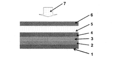
- FIG. 1 It is the schematic (sectional drawing) which shows one Embodiment of the perovskite type solar cell of this invention. Specifically, a negative electrode, a hole blocking layer, a mesoporous metal oxide layer, a perovskite layer, a hole transport layer, and a positive electrode are formed in order, and a schematic diagram showing that light irradiation is performed from the positive electrode side (cross-sectional view) It is.
- Perovskite solar cell of the present invention is composed of the following members.
- a negative electrode, a hole blocking layer, a perovskite layer, a hole transport layer, and a positive electrode are formed in this order, and the negative electrode is made of metal titanium, titanium alloy, and surface-treated metal titanium. And at least one material selected from the group consisting of surface-treated titanium alloys, and light irradiation is performed from the positive electrode side.
- titanium material a material selected from the group consisting of titanium metal, titanium alloy, surface-treated metal titanium, and surface-treated titanium alloy may be simply referred to as titanium material.
- Negative electrode The negative electrode is composed of at least one material selected from the group consisting of titanium metal, titanium alloy, surface-treated metal titanium, and surface-treated titanium alloy.
- Metal titanium materials such as metal titanium and titanium alloys, and materials obtained by surface treatment of these metal titanium materials can be used.
- titanium alloy material the type is not particularly limited.
- the titanium alloy Ti-6Al-4V, Ti-4.5Al-3V-2Fe-2Mo, Ti-0.5Pd and the like are preferable.
- titanium material a material obtained by mirror-treating metal titanium or titanium alloy material by buffing or electrolytic polishing is more preferable.
- the thickness of the negative electrode substrate is usually preferably about 0.01 to 10 mm, more preferably about 0.01 to 5 mm, and further preferably about 0.05 to 1 mm.
- Titanium material has a lower electrical resistance value than a negative electrode on which a conventional transparent conductive film is formed. Therefore, compared with a perovskite solar cell using a conventional transparent conductive film, the titanium material has a large photoelectric conversion efficiency for a large cell area, and as a result, high power can be generated.
- the titanium material used for the negative electrode does not have light transmittance, it is characterized in that light irradiation is performed from the positive electrode.
- a surface treatment such as a physical polishing such as a mirror surface treatment or a chemical polishing such as chemical etching on titanium metal or a titanium alloy.
- Hole blocking layer does not move holes generated by charge separation in the organic-inorganic perovskite compound of the photoelectric conversion layer to the negative electrode side, but only electrons that have been charge separated move to the negative electrode side. It becomes a layer that plays an important role.
- a dense hole blocking layer is required.
- the hole blocking layer preferably has a thickness of about 1 to 500 nm.
- the thickness of the hole blocking layer is more preferably about 1 to 100 nm.
- the hole blocking layer is preferably composed of at least one material selected from the group consisting of an n-type semiconductor, an electron transporting conductive polymer, and an electron transporting inorganic salt.
- the hole blocking layer is preferably an n-type semiconductor.
- the hole blocking layer is preferably composed of at least one material selected from the group consisting of titanium oxide, zinc oxide, zirconium oxide, aluminum oxide, cesium carbonate, fullerene derivatives, graphene derivatives, and perylene derivatives.
- the titanium oxide is preferably titanium oxide prepared by surface treatment of titanium metal or a titanium alloy.
- the surface treatment is preferably at least one surface treatment selected from the group consisting of atmospheric oxidation treatment and anodization treatment for titanium metal or titanium alloy.
- the hole blocking layer is preferably a titanium oxide layer formed by subjecting titanium metal to an oxidation treatment such as atmospheric oxidation treatment or anodizing treatment.
- the atmospheric oxidation treatment temperature is preferably about 300 to 700 ° C. It is preferable to carry out atmospheric oxidation treatment at about 400 to 600 ° C.
- anodic oxidation is performed in an electrolytic solution containing at least one acid selected from the group consisting of inorganic acids and organic acids that do not have an etching action on metal titanium and a salt compound thereof. It is a process of forming an oxide film of titanium.
- the anodization voltage is preferably about 1 to 200V, more preferably about 10 to 100V.
- the electrolytic solution having no etching action on titanium is an electrolytic solution containing at least one compound selected from the group consisting of inorganic acids, organic acids and salts thereof (hereinafter also referred to as inorganic acids). Is preferred.
- the electrolyte solution containing the inorganic acid or the like is preferably a dilute aqueous solution of phosphoric acid or phosphate.
- the organic acid having no etching action on titanium acetic acid, adipic acid, lactic acid and the like are preferable.
- salts of these acids such as sodium dihydrogen phosphate, disodium hydrogen phosphate, sodium hydrogen carbonate, sodium acetate, potassium adipate, sodium lactate and the like can also be used.
- an electrolytic solution containing an electrolyte such as sodium sulfate, potassium sulfate, magnesium sulfate, sodium nitrate, potassium nitrate, magnesium nitrate, calcium nitrate.
- the inorganic acid phosphoric acid and phosphate are most preferable.
- the electrolytic solution is preferably a dilute aqueous solution such as an inorganic acid.
- concentration of the inorganic acid or the like in the electrolytic solution is preferably in the range of about 1% by weight for reasons such as economy.
- a concentration range of about 0.01 to 10% by weight is preferable, a concentration range of about 0.1 to 10% by weight is more preferable, and a concentration range of about 1 to 3% by weight is more preferable.
- these acids may be used alone or in combination of any two or more of these acids regardless of whether they are organic acids or inorganic acids.
- the aqueous solution containing a phosphate and phosphoric acid is mentioned.
- the blending ratio of the acid in the electrolytic solution varies depending on the type of acid and acid salt to be used, anodization conditions, etc., but is generally preferably about 0.01 to 10% by weight, preferably 0.1 to 10% by weight in terms of the total amount of the acid. % Is more preferable, and about 1 to 3% by weight is more preferable.
- the titanium oxide is preferably titanium oxide prepared by subjecting a titanium alkoxide compound, which is a titanium oxide precursor, to hydrolysis treatment and heat treatment.
- the hole blocking layer may be formed by coating a titanium alkoxide compound, which is a titanium oxide precursor, on a material not treated with titanium metal, followed by hydrolysis and heat treatment.
- the titanium oxide is preferably titanium oxide prepared by surface treatment with an aqueous titanium tetrachloride solution.
- a denser hole blocking layer is formed, and the hole blocking effect is enhanced.
- the hole blocking layer is preferably made of at least one material selected from the group consisting of electron transporting conductive polymers such as fullerene derivatives and electron transporting inorganic salts such as cesium carbonate.
- titanium oxide in addition to titanium oxide, it may be composed of inorganic n-type semiconductors such as zinc oxide, zirconium oxide, aluminum oxide and cesium carbonate, and organic n-type semiconductors such as fullerene derivatives, graphene derivatives and perylene derivatives.
- inorganic n-type semiconductors such as zinc oxide, zirconium oxide, aluminum oxide and cesium carbonate
- organic n-type semiconductors such as fullerene derivatives, graphene derivatives and perylene derivatives.
- a mesoporous metal oxide layer is preferably formed between the hole blocking layer and the perovskite layer.
- the mesoporous metal oxide layer has a porous structure with fine pores. For this reason, it is preferable to support the organic-inorganic perovskite compound, which is a photoelectric conversion layer, evenly in the mesoporous metal oxide layer.
- the thickness of the mesoporous metal oxide layer is preferably about 5 to 5,000 nm, and more preferably about 100 to 500 nm.
- the mesoporous metal oxide layer is preferably composed of at least one material selected from the group consisting of titanium oxide, aluminum oxide, zirconium oxide and niobium oxide.
- the paste is preferably heat-treated at 100 to 600 ° C. after coating treatment such as spin coating, dip coating, screen printing, and air spraying.
- a hole blocking layer can be obtained by heat treating the titanium oxide, aluminum oxide, zirconium oxide, and niobium oxide powder pastes by spin coating, dip coating, screen printing, air spraying, etc., followed by heat treatment at 100-600 ° C. It is also possible to form a mesoporous metal oxide between the perovskite layer and the perovskite layer.
- the perovskite layer is a charge separation layer.
- the thickness of the perovskite layer is preferably about 5 to 10,000 nm, and more preferably about 50 to 500 nm.
- the perovskite layer is composed of RNH 3 PbX 3 , R (NH 2 ) 2 PbX 3 , RNH 3 SnX 3 and R (NH 2 ) 2 SnX 3 (R is an alkyl group, X is a group consisting of Cl, Br and I. It is preferably made of at least one material selected from the group consisting of at least one selected halogen.
- R in RNH 3 PbX 3 , R (NH 2 ) 2 PbX 3 , RNH 3 SnX 3 and R (NH 2 ) 2 SnX 3 is an alkyl group, and preferably has a linear or branched structure.
- R include a methyl group, an ethyl group, a propyl group, an isopropyl group, a butyl group, a tert-butyl group, a pentyl group, a hexyl group, an octyl group, a nonyl group, and a dodecyl group.
- X in RNH 3 PbX 3 , R (NH 2 ) 2 PbX 3 , RNH 3 SnX 3 and R (NH 2 ) 2 SnX 3 is a halogen, preferably a halogen selected from the group consisting of Cl, Br and I; A combination of a plurality of selected halogens is preferred.
- RNH 3 PbX 3 (R is an alkyl group and X is at least one halogen selected from the group consisting of Cl, Br and I) is preferably CH 3 NH 3 PbI 3 .
- the perovskite layer is more preferably dark brown and CH 3 NH 3 PbI 3 that absorbs all visible light from 300 nm to 800 nm.
- RNH 3 PbX 3 (R is an alkyl group, X is at least one halogen selected from the group consisting of Cl, Br and I), but CH 3 NH 3 PbI 3-n Cl n (n is 0 to 3 It is preferable that More preferably, the use of CH 3 NH 3 PbI 3-n Cl n (where n is from 0 to 3) not only simplifies the coating technique, but also diffuses electrons and holes generated in the perovskite crystal due to light absorption. The length is increased and the photoelectric conversion efficiency is improved.
- an alkylamine halide, lead halide, and tin halide are dissolved in a solvent.
- Halogen is at least one halogen selected from the group consisting of Cl, Br and I.
- the dissolved material is coated by a spray method, a spin coating method, a dip coating method, a die coating method or the like and then dried.
- a perovskite layer which is a charge separation layer formed by vapor deposition.
- the solvent examples include esters such as ⁇ -butyllactone, methyl formate, and ethyl acetate; ketones such as acetone and dimethyl ketone; ethers such as diethyl ether and diisopropyl ether; alcohols such as methanol and ethanol; Halogenated hydrocarbons such as ethylene chloride and chloroform; nitrile solvents such as acetonitrile and propionitrile; N, N-dimethylformamide, dimethyl sulfoxide and the like can be preferably used.
- esters such as ⁇ -butyllactone, methyl formate, and ethyl acetate
- ketones such as acetone and dimethyl ketone
- ethers such as diethyl ether and diisopropyl ether
- alcohols such as methanol and ethanol
- Halogenated hydrocarbons such as ethylene chloride and chloroform
- nitrile solvents such as acetonitrile and
- Hole transport layer is important for moving the holes to the positive electrode side without moving the electrons generated by the charge separation with the organic / inorganic perovskite compound in the photoelectric conversion layer to the positive electrode. A layer that plays a role.
- the hole transport layer is preferably a p-type semiconductor, and the thickness thereof is preferably about 1 to 5,000 nm, more preferably about 1 to 300 nm.
- the hole transport layer is preferably composed of a p-type semiconductor.
- the hole transport layer is preferably composed of at least one material selected from the group consisting of spiro-OMeTAD derivatives, molybdenum oxide, vanadium oxide, copper iodide, copper thiocyanate, polythiophene and polytriphenylamine.
- Spiro-OMeTAD derivatives are 2,2 ', 7,7'-tetrakis (N, N-di-p-methoxyphenylamino) -9,9'-spirobifluorene and derivatives of the same compound.
- the hole transport layer is preferably a hole transport layer prepared by doping with at least one material selected from the group consisting of oxygen, lithium compounds, cobalt compounds, vanadium compounds and molybdenum compounds. More preferably, the material to be doped is at least one material selected from the group consisting of vanadium compounds and molybdenum compounds.
- the component in which the component for forming the hole transport layer is dissolved in a solvent is coated by a spray method, a spin coating method, a dip coating method, etc. and then dried. It is preferable to form a transport layer.
- the solvent examples include esters such as ⁇ -butyllactone, methyl formate, and ethyl acetate; ketones such as acetone and dimethyl ketone; ethers such as diethyl ether and diisopropyl ether; alcohols such as methanol and ethanol Halogenated hydrocarbons such as ethylene chloride and chloroform; nitrile solvents such as acetonitrile and propionitrile; hydrocarbon solvents such as chlorobenzene, dichlorobenzene and toluene can be preferably used.
- esters such as ⁇ -butyllactone, methyl formate, and ethyl acetate
- ketones such as acetone and dimethyl ketone
- ethers such as diethyl ether and diisopropyl ether
- alcohols such as methanol and ethanol
- Halogenated hydrocarbons such as ethylene chloride and chloroform
- nitrile solvents such as aceton
- Positive electrode Positive electrode is gold, silver, aluminum, tin-doped indium oxide (ITO), fluorine-doped tin oxide (FTO), tin oxide (SnO 2 ), indium zinc oxide (IZO), zinc oxide (ZnO), It is preferably composed of at least one material selected from the group consisting of aluminum-doped zinc (AZO), PEDOT: PSS, graphene, carbon nanotubes, and polyaniline.
- ITO indium oxide
- FTO fluorine-doped tin oxide
- SnO 2 tin oxide
- IZO indium zinc oxide
- ZnO zinc oxide
- It is preferably composed of at least one material selected from the group consisting of aluminum-doped zinc (AZO), PEDOT: PSS, graphene, carbon nanotubes, and polyaniline.
- PSS is a mixture obtained by adding poly (ethylene sulfonic acid) (PSS), which is a polymer electrolyte, to PEDOT (poly -3-4- ethylenedioxythiophene) exhibiting good conductive properties.
- the positive electrode preferably has a thin film shape, a nanowire shape, or a grid shape.
- the thickness of the positive electrode is preferably about 1 to 1,000 nm, more preferably about 1 to 300 nm.
- the positive electrode film forming method it is preferable to coat by vapor deposition, sputtering, spray method, spin coating method, dip coating method or the like.
- the perovskite solar cell of the present invention uses a titanium material having no optical transparency for the negative electrode, light irradiation is performed from the positive electrode side.
- the positive electrode preferably has an opening.
- the area of the opening of the positive electrode is preferably about 50 to 99%, more preferably about 90 to 99% with respect to the area of the positive electrode.
- the perovskite solar cell is preferably subjected to antireflection film processing in order to improve light transmittance.
- a negative electrode, a hole blocking layer, a perovskite layer, a hole transport layer, a positive electrode, and an antireflection film are preferably formed in this order.
- the antireflection film is preferably made of at least one material selected from the group consisting of molybdenum oxide (MoOx), magnesium fluoride (MgF 2 ), and lithium fluoride (LiF).
- MoOx molybdenum oxide
- MgF 2 magnesium fluoride
- LiF lithium fluoride
- coating is preferably performed by vapor deposition, sputtering, spraying, spin coating, dip coating, or the like.
- the perovskite solar cell of the present invention performs light irradiation from the positive electrode side.
- the perovskite solar cell preferably has a condensing device arranged on the positive electrode side.
- the condensing device is disposed on the positive electrode or antireflection film side. Furthermore, high power generation corresponding to high photoelectric conversion efficiency is possible.
- the light irradiation means is arranged from the positive electrode or the antireflection film side through the light collecting device.
- the condensing rate when the incident light is converged by using a condensing device is preferably about 110 to 5,000%, more preferably about 200 to 4,000%, further preferably about 300 to 3,000%, and about 500 to 900%. Particularly preferred.
- setting the condensing rate to 500% means converging the original incident light by five times using the condensing device.
- the condensing device is not particularly limited, but a condensing lens such as a linear Fresnel lens made of transparent plastics such as glass, PMMA (Polymethyl methacrylate), PET (Polyethylene terephthalate), PEN (Polyethylene naphthalate) is used. It is preferable to use it.
- a condensing lens such as a linear Fresnel lens made of transparent plastics such as glass, PMMA (Polymethyl methacrylate), PET (Polyethylene terephthalate), PEN (Polyethylene naphthalate) is used. It is preferable to use it.
- the perovskite solar cell preferably includes a power storage device.
- a secondary battery that uses lead dioxide (PbO 2 ) for the positive electrode, lead (Pb) for the negative electrode, and dilute sulfuric acid (H 2 SO 4 ) for the electrolyte, as a storage battery that stores DC power generated by the perovskite solar cell.
- PbO 2 lead dioxide
- Pb lead
- H 2 SO 4 dilute sulfuric acid
- NiOOH nickel oxyhydroxide
- hydrogen storage alloy for the negative electrode
- nickel-metal hydride battery that uses an alkaline aqueous solution of potassium hydroxide for the electrolyte
- lithium-containing metal oxide for the positive electrode
- Lithium battery which is a secondary battery using a carbon material such as graphite, and an organic electrolyte as an electrolyte
- NAS battery which is a secondary battery using sulfur as a positive electrode, sodium as a negative electrode, and ⁇ -alumina as an electrolyte; It is preferable to select arbitrarily.
- the characteristics of hydrogen that can be easily stored and transported can be utilized.
- Example 1 As a negative electrode , a titanium material (25 mm ⁇ 25 mm ⁇ 1 mm) obtained by mirror-treating metallic titanium was ultrasonically cleaned with acetone for 15 minutes. Subsequently, it was ultrasonically washed with ethanol for 15 minutes and then dried. Next, oxygen flow (0.05 MPa, 5 minutes) was performed in a UV ozone cleaner UV253S (manufactured by Filgen). UV irradiation was then performed for 30 minutes followed by a nitrogen flow (0.2 MPa, 7.5 minutes).
- Titanium oxide paste (Dyesol 18NR-T) was dispersed in ethanol at a weight ratio of 2: 7. Next, 50 ⁇ L of this solution was dropped on the titanium material on which the hole blocking layer was formed, and coating was performed at 3,000 rpm for 40 seconds using a spin coater. Next, heat treatment was performed at 500 ° C. for 15 minutes to produce a mesoporous metal oxide layer.
- a Spiro-OMeTAD chlorobenzene solution was dropped over the titanium material on which the perovskite layer was formed, and then coated at 3,000 rpm for 40 seconds using a spin coater. Thereafter, it was left for 12 hours in the presence of oxygen.
- Example 2 As a negative electrode , a titanium material (25 mm ⁇ 25 mm ⁇ 1 mm) obtained by mirror-treating metallic titanium was ultrasonically cleaned with acetone for 15 minutes. Subsequently, it was ultrasonically washed with ethanol for 15 minutes and then dried. Next, oxygen flow (0.05 MPa, 5 minutes) was performed in a UV ozone cleaner UV253S (manufactured by Filgen). UV irradiation was then performed for 30 minutes followed by a nitrogen flow (0.2 MPa, 7.5 minutes).
- a Spiro-OMeTAD chlorobenzene solution was dropped over the titanium material on which the perovskite layer was formed, and then coated at 3,000 rpm for 40 seconds using a spin coater.
- molybdenum oxide manufactured by Wako Pure Chemical Industries, Ltd.
- a thickness of 10 nm was vapor-deposited to a thickness of 10 nm (dope) in order to improve the hole transport efficiency using a vapor deposition apparatus and to prevent the perovskite layer from deteriorating, thereby producing a hole transport layer.
- Example 2 Compared with Example 1, in Example 2, the hole blocking layer was produced by a simple technique in which a mirror-treated metal titanium was heated at 500 ° C. for 20 minutes.
- Example 1 Nevertheless, a photoelectric conversion efficiency more than twice that of Example 1 was obtained. Improvement by photoelectric conversion efficiency by depositing molybdenum oxide on hole transport layer, changing gold to silver as counter electrode, changing film thickness of deposition, depositing molybdenum oxide as antireflection film, etc. was recognized.
- Example 3 As a negative electrode , a titanium material (25 mm ⁇ 25 mm ⁇ 1 mm) obtained by mirror-treating metallic titanium was ultrasonically cleaned with acetone for 15 minutes. Subsequently, it was ultrasonically washed with ethanol for 15 minutes and then dried. Next, oxygen flow (0.05 MPa, 5 minutes) was carried out in a UV ozone cleaner UV253S (manufactured by Philgen). UV irradiation was then performed for 30 minutes followed by a nitrogen flow (0.2 MPa, 7.5 minutes).
- This solution was dropped over the titanium material on which the metal oxide layer was formed, and then coated at 3,000 rpm for 80 seconds using a spin coater. Then, it was dried at 80 ° C. for 30 minutes. Next, heat treatment was performed at 100 ° C. for 90 minutes to produce a perovskite layer.
- a Spiro-OMeTAD chlorobenzene solution was dropped over the titanium material on which the perovskite layer was formed, and then coated at 3,000 rpm for 40 seconds using a spin coater.
- molybdenum oxide manufactured by Wako Pure Chemical Industries, Ltd.
- a hole transport layer was produced.
- Example 4 As a negative electrode , a titanium material (25 mm ⁇ 25 mm ⁇ 1 mm) obtained by mirror-treating metallic titanium was ultrasonically cleaned with acetone for 15 minutes. Further, it was ultrasonically washed with ethanol for 15 minutes and then dried. Next, oxygen flow (0.05 MPa, 5 minutes) was performed in a UV ozone cleaner UV253S (manufactured by Filgen). UV irradiation was then performed for 30 minutes followed by a nitrogen flow (0.2 MPa, 7.5 minutes).
- a Spiro-OMeTAD chlorobenzene solution was dropped over the titanium material on which the perovskite layer was formed, and then coated at 3,000 rpm for 40 seconds using a spin coater.
- molybdenum oxide manufactured by Wako Pure Chemical Industries, Ltd.
- a vapor deposition device to prevent the perovskite layer from deteriorating to produce a hole transport layer.
- Example 5 As a negative electrode , a titanium material (25 mm ⁇ 25 mm ⁇ 1 mm) obtained by mirror-treating metallic titanium was ultrasonically cleaned with acetone for 15 minutes. Further, it was ultrasonically washed with ethanol for 15 minutes and then dried. Next, oxygen flow (0.05 MPa, 5 minutes) was performed in a UV ozone cleaner UV253S (manufactured by Filgen). UV irradiation was then performed for 30 minutes followed by a nitrogen flow (0.2 MPa, 7.5 minutes).
- This solution was dropped over the titanium material on which the metal oxide layer was formed, and then coated at 2,000 rpm for 80 seconds using a spin coater. Then, it was dried at 80 ° C. for 30 minutes. Next, heat treatment was performed at 100 ° C. for 90 minutes to produce a perovskite layer.
- hole transport layer 80 mg of spiro-OMeTAD was dissolved in 1 mL of chlorobenzene. 17.5 ⁇ L of a solution in which 520 mg of Li-TFSI was dissolved in 1 mL of acetonitrile and 28.8 ⁇ L of tert-butylpyridine were added. Next, this solution was dropped over the titanium material on which the perovskite layer was formed, and then coated at 3,000 rpm for 40 seconds using a spin coater.
- molybdenum oxide manufactured by Wako Pure Chemical Industries, Ltd.
- a vapor deposition apparatus thereby preparing a hole transport layer.
- Example 6 As a negative electrode , a titanium material (25 mm ⁇ 25 mm ⁇ 1 mm) obtained by mirror-treating metallic titanium was ultrasonically cleaned with acetone for 15 minutes. Further, it was ultrasonically washed with ethanol for 15 minutes and then dried. Next, oxygen flow (0.05 MPa, 5 minutes) was performed in a UV ozone cleaner UV253S (manufactured by Filgen). UV irradiation was then performed for 30 minutes followed by a nitrogen flow (0.2 MPa, 7.5 minutes).
- This solution was dropped over the titanium material on which the metal oxide layer was formed, and then coated at 2,000 rpm for 80 seconds using a spin coater. Then, it was dried at 80 ° C. for 30 minutes. Next, heat treatment was performed at 100 ° C. for 90 minutes to produce a perovskite layer.
- This solution was dropped over the titanium material on which the perovskite layer was formed, and then coated at 3,000 rpm for 40 seconds using a spin coater.
- molybdenum oxide manufactured by Wako Pure Chemical Industries, Ltd.
- a hole transport layer was produced.
- Example 7 As a negative electrode , a titanium material (25 mm ⁇ 25 mm ⁇ 1 mm) obtained by mirror-treating metallic titanium was ultrasonically cleaned with acetone for 15 minutes. Further, it was ultrasonically washed with ethanol for 15 minutes and then dried. Subsequently, oxygen flow (0.05 MPa, 5 minutes) was performed in a UV ozone cleaner UV253S (manufactured by Filgen), followed by ultraviolet irradiation for 30 minutes, and then nitrogen flow (0.2 MPa, 7.5 minutes).
- UV ozone cleaner UV253S manufactured by Filgen
- titanium material was anodized at 10 V, 30 V, 50 V, 100 V or 150 V in 1 wt% phosphoric acid for 10 minutes, respectively, to form a titanium oxide layer on the surface of the titanium material. .
- the substrate was washed with 0.04M TiCl 4 aqueous solution, allowed to stand at 80 ° C. for 30 minutes, and then washed with pure water and ethanol.
- This solution was dropped over the titanium material on which the metal oxide layer was formed, and then coated at 2,000 rpm for 80 seconds using a spin coater. Then, it was dried at 80 ° C. for 30 minutes. Next, heat treatment was performed at 100 ° C. for 90 minutes to produce a perovskite layer.
- a Spiro-OMeTAD chlorobenzene solution was dropped over the titanium material on which the perovskite layer was formed, and then coated at 3,000 rpm for 40 seconds using a spin coater.
- molybdenum oxide manufactured by Wako Pure Chemical Industries, Ltd.
- a vapor deposition apparatus thereby preparing a hole transport layer.
- Example 8 As a negative electrode , a titanium material (25 mm ⁇ 25 mm ⁇ 1 mm) obtained by mirror-treating metallic titanium was ultrasonically cleaned with acetone for 15 minutes. Further, it was ultrasonically washed with ethanol for 15 minutes and then dried. Next, oxygen flow (0.05 MPa, 5 minutes) was performed in a UV ozone cleaner UV253S (manufactured by Filgen). UV irradiation was then performed for 30 minutes followed by a nitrogen flow (0.2 MPa, 7.5 minutes).
- titanium material was anodized in 1% by weight phosphoric acid at 10V or 30V for 10 minutes, respectively, to form a titanium oxide layer on the surface of the titanium material.
- Titanium oxide paste (Dyesol 18NR-T) was dispersed in ethanol at a weight ratio of 2: 7. 50 ⁇ L of this solution was dropped onto the titanium material on which the hole blocking layer was formed, and an operation of coating with a spin coater at 3,000 rpm for 40 seconds was performed.
- This solution was dropped over the titanium material on which the metal oxide layer was formed, and then coated at 2,000 rpm for 80 seconds using a spin coater. Then, it was dried at 80 ° C. for 30 minutes. Next, heat treatment was performed at 100 ° C. for 90 minutes to produce a perovskite layer.
- a Spiro-OMeTAD chlorobenzene solution was dropped over the titanium material on which the perovskite layer was formed, and then coated at 3,000 rpm for 40 seconds using a spin coater.
- molybdenum oxide manufactured by Wako Pure Chemical Industries
- vapor-deposited by 10 nm was vapor-deposited by 10 nm in order to improve the hole transport efficiency and to prevent the perovskite layer from deteriorating, thereby preparing a hole transport layer.
Landscapes
- Engineering & Computer Science (AREA)
- Power Engineering (AREA)
- Microelectronics & Electronic Packaging (AREA)
- Photovoltaic Devices (AREA)
Abstract
L'objectif de la présente invention est de résoudre des problèmes tels que la dégradation optique d'un colorant sensibilisateur qui est une préoccupation dans une cellule solaire à colorant, la volatilisation d'une solution électrolytique, la faible durabilité due à des fuites, et le coût de fabrication élevé qui est une préoccupation dans des cellules solaires au silicium et des cellules solaires à semi-conducteur composé. L'invention porte sur une cellule solaire pérovskite dans laquelle une électrode négative, une couche de blocage de trous, une couche de pérovskite, une couche de transport de trous et une électrode positive sont formées séquentiellement. La cellule solaire pérovskite est caractérisée en ce que : l'électrode négative comprend au moins un type de matériau choisi dans un groupe comprenant le titane métallique, un alliage de titane, du titane métallique soumis à un traitement de surface, et un alliage de titane soumis à un traitement de surface ; et l'électrode positive est exposée à la lumière.
Applications Claiming Priority (2)
| Application Number | Priority Date | Filing Date | Title |
|---|---|---|---|
| JP2015-134570 | 2015-07-03 | ||
| JP2015134570A JP6352223B2 (ja) | 2015-07-03 | 2015-07-03 | ペロブスカイト型太陽電池の製造方法 |
Publications (1)
| Publication Number | Publication Date |
|---|---|
| WO2017006839A1 true WO2017006839A1 (fr) | 2017-01-12 |
Family
ID=57685458
Family Applications (1)
| Application Number | Title | Priority Date | Filing Date |
|---|---|---|---|
| PCT/JP2016/069516 WO2017006839A1 (fr) | 2015-07-03 | 2016-06-30 | Cellule solaire pérovskite |
Country Status (2)
| Country | Link |
|---|---|
| JP (1) | JP6352223B2 (fr) |
| WO (1) | WO2017006839A1 (fr) |
Cited By (7)
| Publication number | Priority date | Publication date | Assignee | Title |
|---|---|---|---|---|
| CN106910829A (zh) * | 2017-03-08 | 2017-06-30 | 新乡学院 | 一种柔性太阳能电池的制备方法 |
| CN108286833A (zh) * | 2018-01-05 | 2018-07-17 | 山东省圣泉生物质石墨烯研究院 | 黑色体吸收型涂层、包含其的光热转化部件及太阳能热水器 |
| CN108793196A (zh) * | 2018-03-01 | 2018-11-13 | 复旦大学 | 银盐和铈盐共掺杂的硫氰酸亚铜复合薄膜及其制备方法和应用 |
| CN109742236A (zh) * | 2018-12-13 | 2019-05-10 | 东莞理工学院 | 一种离子液体增敏的钙钛矿太阳能电池及其制备方法 |
| CN109932337A (zh) * | 2017-12-18 | 2019-06-25 | 有研半导体材料有限公司 | 一种用于评价硅基背封膜致密性的装置和方法 |
| CN112955992A (zh) * | 2018-09-21 | 2021-06-11 | 环境光子学公司 | 染料敏化的光伏电池 |
| CN116282135A (zh) * | 2023-02-27 | 2023-06-23 | 吉林大学 | 一种Cu掺杂Ga2-XInXO3固溶体纳米材料的制备方法及应用 |
Families Citing this family (7)
| Publication number | Priority date | Publication date | Assignee | Title |
|---|---|---|---|---|
| JP6725219B2 (ja) * | 2015-07-31 | 2020-07-15 | 積水化学工業株式会社 | 太陽電池 |
| JP2018157147A (ja) * | 2017-03-21 | 2018-10-04 | 積水化学工業株式会社 | 固体接合型光電変換素子 |
| JP6995596B2 (ja) * | 2017-12-08 | 2022-01-14 | 住友化学株式会社 | 光電変換素子 |
| WO2020105207A1 (fr) | 2018-11-20 | 2020-05-28 | パナソニックIpマネジメント株式会社 | Batterie solaire |
| JP7429881B2 (ja) | 2019-04-16 | 2024-02-09 | パナソニックIpマネジメント株式会社 | 太陽電池 |
| JP2021077788A (ja) * | 2019-11-11 | 2021-05-20 | 三菱ケミカル株式会社 | 光電変換素子 |
| WO2021181842A1 (fr) | 2020-03-12 | 2021-09-16 | パナソニックIpマネジメント株式会社 | Pile solaire |
Citations (5)
| Publication number | Priority date | Publication date | Assignee | Title |
|---|---|---|---|---|
| WO2009139310A1 (fr) * | 2008-05-12 | 2009-11-19 | コニカミノルタホールディングス株式会社 | Cellule solaire à colorant et son procédé de fabrication |
| JP2014026903A (ja) * | 2012-07-30 | 2014-02-06 | Sharp Corp | 光電変換素子および色素増感太陽電池 |
| WO2014045021A1 (fr) * | 2012-09-18 | 2014-03-27 | Isis Innovation Limited | Dispositif optoélectronique |
| WO2015064774A2 (fr) * | 2014-01-27 | 2015-05-07 | 株式会社昭和 | Cellule solaire sensibilisée par colorant équipée d'une unité de condensation de faisceau |
| JP2016139805A (ja) * | 2015-01-27 | 2016-08-04 | 積水化学工業株式会社 | 太陽電池及び有機半導体材料 |
Family Cites Families (5)
| Publication number | Priority date | Publication date | Assignee | Title |
|---|---|---|---|---|
| JP2004071682A (ja) * | 2002-08-02 | 2004-03-04 | Casio Electronics Co Ltd | 無機−有機薄膜複合材料 |
| JP4317381B2 (ja) * | 2003-04-18 | 2009-08-19 | Tdk株式会社 | 光電変換用酸化物半導体電極の製造方法 |
| JP4608030B2 (ja) * | 2009-03-10 | 2011-01-05 | 昭和電工株式会社 | 透明導電性材料の製造方法 |
| US20160071655A1 (en) * | 2013-04-04 | 2016-03-10 | The Regents Of The University Of California | Electrochemical solar cells |
| JP6304980B2 (ja) * | 2013-09-10 | 2018-04-04 | 大阪瓦斯株式会社 | ペロブスカイト系材料を用いた光電変換装置 |
-
2015
- 2015-07-03 JP JP2015134570A patent/JP6352223B2/ja active Active
-
2016
- 2016-06-30 WO PCT/JP2016/069516 patent/WO2017006839A1/fr active Application Filing
Patent Citations (5)
| Publication number | Priority date | Publication date | Assignee | Title |
|---|---|---|---|---|
| WO2009139310A1 (fr) * | 2008-05-12 | 2009-11-19 | コニカミノルタホールディングス株式会社 | Cellule solaire à colorant et son procédé de fabrication |
| JP2014026903A (ja) * | 2012-07-30 | 2014-02-06 | Sharp Corp | 光電変換素子および色素増感太陽電池 |
| WO2014045021A1 (fr) * | 2012-09-18 | 2014-03-27 | Isis Innovation Limited | Dispositif optoélectronique |
| WO2015064774A2 (fr) * | 2014-01-27 | 2015-05-07 | 株式会社昭和 | Cellule solaire sensibilisée par colorant équipée d'une unité de condensation de faisceau |
| JP2016139805A (ja) * | 2015-01-27 | 2016-08-04 | 積水化学工業株式会社 | 太陽電池及び有機半導体材料 |
Non-Patent Citations (1)
| Title |
|---|
| J. TROUGHTON ET AL.: "Highly efficient, flexible, indium-free perovskite solar cells employing metallic substrates", JOURNAL OF MATERIALS CHEMISTRY A, vol. 3, no. 17, 7 May 2015 (2015-05-07), pages 9141 - 9145, XP055345443 * |
Cited By (9)
| Publication number | Priority date | Publication date | Assignee | Title |
|---|---|---|---|---|
| CN106910829A (zh) * | 2017-03-08 | 2017-06-30 | 新乡学院 | 一种柔性太阳能电池的制备方法 |
| CN109932337A (zh) * | 2017-12-18 | 2019-06-25 | 有研半导体材料有限公司 | 一种用于评价硅基背封膜致密性的装置和方法 |
| CN109932337B (zh) * | 2017-12-18 | 2021-08-03 | 有研半导体硅材料股份公司 | 一种用于评价硅基背封膜致密性的装置和方法 |
| CN108286833A (zh) * | 2018-01-05 | 2018-07-17 | 山东省圣泉生物质石墨烯研究院 | 黑色体吸收型涂层、包含其的光热转化部件及太阳能热水器 |
| CN108793196A (zh) * | 2018-03-01 | 2018-11-13 | 复旦大学 | 银盐和铈盐共掺杂的硫氰酸亚铜复合薄膜及其制备方法和应用 |
| CN112955992A (zh) * | 2018-09-21 | 2021-06-11 | 环境光子学公司 | 染料敏化的光伏电池 |
| CN112955992B (zh) * | 2018-09-21 | 2024-04-02 | 环境光子学公司 | 染料敏化的光伏电池 |
| CN109742236A (zh) * | 2018-12-13 | 2019-05-10 | 东莞理工学院 | 一种离子液体增敏的钙钛矿太阳能电池及其制备方法 |
| CN116282135A (zh) * | 2023-02-27 | 2023-06-23 | 吉林大学 | 一种Cu掺杂Ga2-XInXO3固溶体纳米材料的制备方法及应用 |
Also Published As
| Publication number | Publication date |
|---|---|
| JP2017017252A (ja) | 2017-01-19 |
| JP6352223B2 (ja) | 2018-07-04 |
Similar Documents
| Publication | Publication Date | Title |
|---|---|---|
| JP6352223B2 (ja) | ペロブスカイト型太陽電池の製造方法 | |
| Ye et al. | Recent advances in quantum dot-sensitized solar cells: insights into photoanodes, sensitizers, electrolytes and counter electrodes | |
| Huang et al. | Low-temperature processed SnO2 compact layer by incorporating TiO2 layer toward efficient planar heterojunction perovskite solar cells | |
| Ke et al. | Cooperative tin oxide fullerene electron selective layers for high-performance planar perovskite solar cells | |
| EP3172776B1 (fr) | Structure mésoscopique pour dispositif de conversion photoélectrique à base de pérovskite organique-inorganique et son procédé de fabrication | |
| Raj et al. | Improved photovoltaic performance of CdSe/CdS/PbS quantum dot sensitized ZnO nanorod array solar cell | |
| Lin et al. | Photoactive p-type PbS as a counter electrode for quantum dot-sensitized solar cells | |
| Chen et al. | Electrodeposited nanoporous ZnO films exhibiting enhanced performance in dye-sensitized solar cells | |
| Xie et al. | Electrolyte effects on electron transport and recombination at ZnO nanorods for dye-sensitized solar cells | |
| JP6141054B2 (ja) | 有機−無機ナノハイブリッド光電変換装置 | |
| Zhang et al. | Influence of different TiO2 blocking films on the photovoltaic performance of perovskite solar cells | |
| US20070119498A1 (en) | Electrode for solar cells, manufacturing method thereof and solar cell comprising the same | |
| Wu et al. | Electrochemical formation of transparent nanostructured TiO 2 film as an effective bifunctional layer for dye-sensitized solar cells | |
| Karuppuchamy et al. | Cathodic electrodeposition of TiO2 thin films for dye-sensitized photoelectrochemical applications | |
| Tao et al. | Polyoxometalate doped tin oxide as electron transport layer for low cost, hole-transport-material-free perovskite solar cells | |
| Park et al. | Performance enhancement of dye-sensitized solar cell with a TiCl 4-treated TiO 2 compact layer | |
| KR101540364B1 (ko) | Zso 기반 페로브스카이트 태양전지 및 이의 제조방법 | |
| Soultati et al. | Organic solar cells of enhanced efficiency and stability using zinc oxide: zinc tungstate nanocomposite as electron extraction layer | |
| Jiang et al. | Efficiency enhancement of perovskite solar cells by fabricating as-prepared film before sequential spin-coating procedure | |
| Zheng et al. | Surface states in TiO 2 submicrosphere films and their effect on electron transport | |
| Venkatesan et al. | Quasi-solid-state composite electrolytes with Al2O3 and ZnO nanofillers for dye-sensitized solar cells | |
| Raj et al. | Electrochemical properties of TiO2 encapsulated ZnO nanorod aggregates dye sensitized solar cells | |
| Elibol et al. | Improving the performance of CdTe QDSSCs by chloride treatment and parameter optimization | |
| KR101794988B1 (ko) | 페로브스카이트 광흡수층 제조방법 및 이를 적용한 태양전지 제조방법 | |
| Liu et al. | Effect of the nature of cationic precursors for SILAR deposition on the performance of CdS and PbS/CdS quantum dot-sensitized solar cells |
Legal Events
| Date | Code | Title | Description |
|---|---|---|---|
| 121 | Ep: the epo has been informed by wipo that ep was designated in this application |
Ref document number: 16821308 Country of ref document: EP Kind code of ref document: A1 |
|
| NENP | Non-entry into the national phase |
Ref country code: DE |
|
| 122 | Ep: pct application non-entry in european phase |
Ref document number: 16821308 Country of ref document: EP Kind code of ref document: A1 |