WO2016208305A1 - コイル部品の製造方法 - Google Patents
コイル部品の製造方法 Download PDFInfo
- Publication number
- WO2016208305A1 WO2016208305A1 PCT/JP2016/065172 JP2016065172W WO2016208305A1 WO 2016208305 A1 WO2016208305 A1 WO 2016208305A1 JP 2016065172 W JP2016065172 W JP 2016065172W WO 2016208305 A1 WO2016208305 A1 WO 2016208305A1
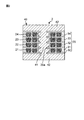
- Authority
- WO
- WIPO (PCT)
- Prior art keywords
- sacrificial conductor
- insulating resin
- spiral wiring
- metal layer
- opening
- Prior art date
- Legal status (The legal status is an assumption and is not a legal conclusion. Google has not performed a legal analysis and makes no representation as to the accuracy of the status listed.)
- Ceased
Links
Images













Classifications
-
- H—ELECTRICITY
- H05—ELECTRIC TECHNIQUES NOT OTHERWISE PROVIDED FOR
- H05K—PRINTED CIRCUITS; CASINGS OR CONSTRUCTIONAL DETAILS OF ELECTRIC APPARATUS; MANUFACTURE OF ASSEMBLAGES OF ELECTRICAL COMPONENTS
- H05K1/00—Printed circuits
- H05K1/16—Printed circuits incorporating printed electric components, e.g. printed resistors, capacitors or inductors
- H05K1/165—Printed circuits incorporating printed electric components, e.g. printed resistors, capacitors or inductors incorporating printed inductors
-
- H—ELECTRICITY
- H01—ELECTRIC ELEMENTS
- H01F—MAGNETS; INDUCTANCES; TRANSFORMERS; SELECTION OF MATERIALS FOR THEIR MAGNETIC PROPERTIES
- H01F41/00—Apparatus or processes specially adapted for manufacturing or assembling magnets, inductances or transformers; Apparatus or processes specially adapted for manufacturing materials characterised by their magnetic properties
- H01F41/02—Apparatus or processes specially adapted for manufacturing or assembling magnets, inductances or transformers; Apparatus or processes specially adapted for manufacturing materials characterised by their magnetic properties for manufacturing cores, coils, or magnets
-
- H—ELECTRICITY
- H01—ELECTRIC ELEMENTS
- H01F—MAGNETS; INDUCTANCES; TRANSFORMERS; SELECTION OF MATERIALS FOR THEIR MAGNETIC PROPERTIES
- H01F17/00—Fixed inductances of the signal type
-
- H—ELECTRICITY
- H01—ELECTRIC ELEMENTS
- H01F—MAGNETS; INDUCTANCES; TRANSFORMERS; SELECTION OF MATERIALS FOR THEIR MAGNETIC PROPERTIES
- H01F41/00—Apparatus or processes specially adapted for manufacturing or assembling magnets, inductances or transformers; Apparatus or processes specially adapted for manufacturing materials characterised by their magnetic properties
- H01F41/02—Apparatus or processes specially adapted for manufacturing or assembling magnets, inductances or transformers; Apparatus or processes specially adapted for manufacturing materials characterised by their magnetic properties for manufacturing cores, coils, or magnets
- H01F41/04—Apparatus or processes specially adapted for manufacturing or assembling magnets, inductances or transformers; Apparatus or processes specially adapted for manufacturing materials characterised by their magnetic properties for manufacturing cores, coils, or magnets for manufacturing coils
-
- H—ELECTRICITY
- H05—ELECTRIC TECHNIQUES NOT OTHERWISE PROVIDED FOR
- H05K—PRINTED CIRCUITS; CASINGS OR CONSTRUCTIONAL DETAILS OF ELECTRIC APPARATUS; MANUFACTURE OF ASSEMBLAGES OF ELECTRICAL COMPONENTS
- H05K2203/00—Indexing scheme relating to apparatus or processes for manufacturing printed circuits covered by H05K3/00
- H05K2203/30—Details of processes not otherwise provided for in H05K2203/01 - H05K2203/17
- H05K2203/308—Sacrificial means, e.g. for temporarily filling a space for making a via or a cavity or for making rigid-flexible PCBs
-
- H—ELECTRICITY
- H05—ELECTRIC TECHNIQUES NOT OTHERWISE PROVIDED FOR
- H05K—PRINTED CIRCUITS; CASINGS OR CONSTRUCTIONAL DETAILS OF ELECTRIC APPARATUS; MANUFACTURE OF ASSEMBLAGES OF ELECTRICAL COMPONENTS
- H05K3/00—Apparatus or processes for manufacturing printed circuits
- H05K3/46—Manufacturing multilayer circuits
- H05K3/4644—Manufacturing multilayer circuits by building the multilayer layer by layer, i.e. build-up multilayer circuits
- H05K3/4682—Manufacture of core-less build-up multilayer circuits on a temporary carrier or on a metal foil
Definitions
- the present invention relates to a method for manufacturing a coil component.
- JP2013-225718A Patent Document 1
- a hole for an inner magnetic path is formed in a substrate, and then spiral wiring is provided on the upper and lower surfaces of the substrate by photolithography or the like.
- an object of the present invention is to provide a method of manufacturing a coil component that can increase the cross-sectional area of the inner magnetic path and obtain a higher inductance value.
- a method of manufacturing a coil component includes Providing a dummy metal layer on the base; Laminating a base insulating resin on the dummy metal layer; Providing an opening in the base insulating resin to expose the dummy metal layer; Providing a first spiral wiring on the base insulating resin, and providing a first sacrificial conductor corresponding to an inner magnetic path on the dummy metal layer in the opening of the base insulating resin; Energizing the first spiral wiring directly or indirectly to enlarge the first spiral wiring by plating, and energizing the dummy metal layer to plate the first sacrificial conductor connected to the dummy metal layer The process of making it larger Covering the first spiral wiring and the first sacrificial conductor with the first insulating resin; Providing an opening in the first insulating resin to expose the first sacrificial conductor; Removing the first sacrificial conductor from the opening of the first insulating
- the first spiral wiring and the first sacrificial conductor are provided in one step. That is, since both the first spiral wiring and the first sacrificial conductor are conductors, they can be formed in one step. Thereby, the total of the tolerance of the position of the hole (sacrificial conductor) for the inner magnetic path with respect to the insulating resin and the tolerance of the position of the spiral wiring with respect to the insulating resin is small. As a result, the cross-sectional area of the inner magnetic path can be increased, and a higher inductance value can be obtained.
- the first spiral wiring is energized directly or indirectly to increase the first spiral wiring by plating, and the dummy metal layer is energized to increase the first sacrificial conductor connected to the dummy metal layer by plating.
- the difference between the thickness of the first spiral wiring and the thickness of the first sacrificial conductor can be eliminated. Therefore, when the opening is provided in the first insulating resin covering the first spiral wiring and the first sacrificial conductor to expose the first sacrificial conductor, the opening is shallow and the opening is easily formed.
- a method for manufacturing a coil component Between the step of exposing the first sacrificial conductor and the step of forming the hole, Providing a second spiral wiring on the first insulating resin, and providing a second sacrificial conductor corresponding to an inner magnetic path on the first sacrificial conductor in the opening of the first insulating resin;
- the second spiral wiring is energized directly or indirectly to enlarge the second spiral wiring by plating, and the dummy metal layer is energized to plate the second sacrificial conductor through the first sacrificial conductor.
- the second spiral wiring and the second sacrificial conductor are provided in one step. That is, since the second spiral wiring and the second sacrificial conductor are both conductors, they can be formed in one step. Thereby, the total of the tolerance of the position of the hole (sacrificial conductor) for the inner magnetic path with respect to the insulating resin and the tolerance of the position of the spiral wiring with respect to the insulating resin is small. As a result, the cross-sectional area of the inner magnetic path can be increased, and a higher inductance value can be obtained.
- the second spiral wiring is energized directly or indirectly to increase the size of the second spiral wiring by plating, and the dummy metal layer is energized to increase the size of the second sacrificial conductor through the first sacrificial conductor. .
- the difference between the thickness of the second spiral wiring and the thickness of the second sacrificial conductor can be eliminated. Therefore, the depth of the opening provided in the second insulating resin is the same as the depth of the opening of the first insulating resin. Furthermore, even if it becomes a multilayer, the depth of an opening part becomes fixed and formation of an opening part becomes easy. Further, the shape of the sacrificial conductor provided in the opening can be made constant.
- the first spiral wiring and the first sacrificial conductor are energized simultaneously
- the second spiral wiring and the second sacrificial conductor are energized simultaneously.
- the plating processing time can be shortened.
- the opening of the base insulating resin and the opening of the first insulating resin are opened in an annular shape.
- the opening of the base insulating resin and the opening of the first insulating resin are opened in an annular shape, the processing load on the opening due to laser processing or the like can be reduced.
- the insulating resin is left in the center of the opening, the sacrificial conductor material to be used can be reduced.
- the insulating resin is not in contact with the base. Therefore, it is possible to prevent delamination due to thermal stress caused by a difference in linear expansion coefficient between the base and the insulating resin during thermal shock or reflow load.
- a method for manufacturing a coil component Providing a dummy metal layer on the base; Laminating a base insulating resin on the dummy metal layer; Providing an opening in the base insulating resin to expose the dummy metal layer; Providing a first spiral wiring on the base insulating resin, and providing a first sacrificial conductor corresponding to an inner magnetic path on the dummy metal layer in the opening of the base insulating resin; Energizing the dummy metal layer to enlarge the first sacrificial conductor connected to the dummy metal layer by plating; Covering the first spiral wiring and the first sacrificial conductor with the first insulating resin; Providing an opening in the first insulating resin to expose the first sacrificial conductor; Removing the first sacrificial conductor from the opening of the first insulating resin by etching to form a hole corresponding to the inner magnetic path; And filling the hole with a magnetic resin and forming the inner magnetic path with
- a method for manufacturing a coil component Between the step of exposing the first sacrificial conductor and the step of forming the hole, Providing a second spiral wiring on the first insulating resin, and providing a second sacrificial conductor corresponding to an inner magnetic path on the first sacrificial conductor in the opening of the first insulating resin; Energizing the dummy metal layer to enlarge the second sacrificial conductor by plating through the first sacrificial conductor; Covering the second spiral wiring and the second sacrificial conductor with the second insulating resin; Providing an opening in the second insulating resin to expose the second sacrificial conductor; In the step of forming the hole, the first sacrificial conductor and the second sacrificial conductor are removed from the opening of the second insulating resin by etching to form a hole corresponding to the inner magnetic path.
- the cross-sectional area of the inner magnetic path can be increased and a higher inductance value can be obtained. it can.
- FIG. 1 is an exploded perspective view showing an electronic component including an embodiment of a coil component of the present invention.
- FIG. 2 is a cross-sectional view of the coil component.
- the electronic component 1 is mounted on an electronic device such as a personal computer, a DVD player, a digital camera, a TV, a mobile phone, or a car electronics.
- the electronic component 1 has two coil components 2 arranged in parallel.
- the coil component 2 includes four layers of spiral wirings 21 to 24, an insulating resin body 35 that covers the four layers of spiral wirings 21 to 24, and a magnetic resin that covers the insulating resin body 35, respectively. 40.
- covering an object means covering at least a part of the object.
- the insulating resin body 35 is omitted.
- the first to fourth spiral wirings 21 to 24 are arranged in order from the lower layer to the upper layer.
- the first to fourth spiral wirings 21 to 24 are each formed in a spiral shape on a plane.
- the first to fourth spiral wirings 21 to 24 are made of a low resistance metal such as Cu, Ag, or Au, for example.
- a spiral wire having a low resistance and a narrow pitch can be formed.
- the insulating resin body 35 includes a base insulating resin 30 and first to fourth insulating resins 31 to 34.
- the base insulating resin 30 and the first to fourth insulating resins 31 to 34 are arranged in order from the lower layer to the upper layer.
- the insulating resins 30 to 34 are made of, for example, an organic insulating material made of an epoxy resin, bismaleimide, liquid crystal polymer, polyimide, or the like, or an inorganic filler material such as a silica filler, or an organic filler made of a rubber material. It is an insulating material consisting of a combination with the above.
- all the insulating resins 30 to 34 are made of the same material. In this embodiment, all the insulating resins 30 to 34 are made of an epoxy resin containing a silica filler.
- the first spiral wiring 21 is laminated on the base insulating resin 30.
- the first insulating resin 31 is laminated on the first spiral wiring 21 and covers the first spiral wiring 21.
- the second spiral wiring 22 is stacked on the first insulating resin 31.
- the second insulating resin 32 is laminated on the second spiral wiring 22 and covers the second spiral wiring 22.
- the third spiral wiring 23 is laminated on the second insulating resin 32.
- the third insulating resin 33 is laminated on the third spiral wiring 23 and covers the third spiral wiring 23.
- the fourth spiral wiring 24 is stacked on the third insulating resin 33.
- the fourth insulating resin 34 is laminated on the fourth spiral wiring 24 and covers the fourth spiral wiring 24.
- the second spiral wiring 22 is connected to the first spiral wiring 21 through a via wiring 25 extending in the stacking direction.
- the via wiring 25 is provided in the first insulating resin 31.
- the inner peripheral end 21 a of the first spiral wiring 21 and the inner peripheral end 22 a of the second spiral wiring 22 are connected via a via wiring 25.
- the outer peripheral end 21b of the first spiral wiring 21 is connected to an external electrode (not shown).
- the outer peripheral end 22b of the second spiral wiring 22 is connected to an external electrode (not shown).
- the fourth spiral wiring 24 is connected to the third spiral wiring 23 through a via wiring 26 extending in the stacking direction.
- the via wiring 26 is provided in the third insulating resin 33.
- the inner peripheral end 23 a of the third spiral wiring 23 and the inner peripheral end 24 a of the fourth spiral wiring 24 are connected via the via wiring 26.
- the outer peripheral end 23b of the third spiral wiring 23 is connected to an external electrode (not shown).
- the outer peripheral end 24b of the fourth spiral wiring 24 is connected to an external electrode (not shown).
- the first to fourth spiral wires 21 to 24 are arranged around the same axis.
- the first spiral wiring 21 and the second spiral wiring 22 are wound in the same direction as viewed from the axial direction (stacking direction).
- the third spiral wiring 23 and the fourth spiral wiring 24 are wound in the same direction as viewed from the axial direction.
- the first and second spiral wirings 21 and 22 and the third and fourth spiral wirings 23 and 24 are wound in opposite directions as viewed from the axial direction.
- the inner and outer surfaces of the first to fourth spiral wires 21 to 24 are covered with an insulating resin body 35.
- the insulating resin body 35 has a hole 35a centered on the same axis of the first to fourth spiral wirings 21 to 24.
- the magnetic resin 40 covers the insulating resin body 35.
- the magnetic resin 40 has an inner portion 41 provided in the hole 35 a of the insulating resin body 35 and an outer portion 42 provided on the outside (outer peripheral surface and upper and lower end surfaces) of the insulating resin body 35.
- the inner portion 41 constitutes an inner magnetic path of the coil component 2
- the outer portion 42 constitutes an outer magnetic path of the coil component 2.
- the material of the magnetic resin 40 is, for example, a resin material containing magnetic powder.
- the magnetic powder is a metal magnetic material such as Fe, Si, or Cr, for example, and the resin material is a resin material such as epoxy, for example.
- the magnetic powder is contained in an amount of 90 wt% or more, and in order to improve the filling properties of the magnetic resin 40, the particle size distribution is different. More preferably, two or three kinds of magnetic powders are mixed.
- a base 50 is prepared.
- the base 50 includes an insulating substrate 51 and base metal layers 52 provided on both surfaces of the insulating substrate 51.
- the insulating substrate 51 is a glass epoxy substrate
- the base metal layer 52 is a Cu foil.
- a dummy metal layer 60 is bonded on the base 50.
- the dummy metal layer 60 is a Cu foil. Since the dummy metal layer 60 is bonded to the base metal layer 52 of the base 50, the dummy metal layer 60 is bonded to the smooth surface of the base metal layer 52. For this reason, the adhesive force of the dummy metal layer 60 and the base metal layer 52 can be weakened, and the base 50 can be easily peeled off from the dummy metal layer 60 in a subsequent process.
- the adhesive that bonds the base 50 and the dummy metal layer 60 is a low-tack adhesive. Further, in order to weaken the adhesive force between the base 50 and the dummy metal layer 60, it is desirable that the interface between the base 50 and the dummy metal layer 60 be a glossy surface.
- the base insulating resin 30 is laminated on the dummy metal layer 60 temporarily fixed to the base 50. At this time, the base insulating resin 30 is laminated by a vacuum laminator and then thermally cured.
- an opening 30a is provided in a part of the base insulating resin 30, and the dummy metal layer 60 is exposed.
- the opening 30a is formed by laser processing.
- the first spiral wiring 21 is provided on the base insulating resin 30, and the first sacrificial conductor 71 corresponding to the inner magnetic path is formed on the dummy metal layer 60 in the opening 30a of the base insulating resin 30. Is provided. At this time, the first spiral wiring 21 and the first sacrificial conductor 71 are simultaneously formed by SAP (Semi-Additive-Process).
- the first spiral wiring 21 is indirectly energized to enlarge the first spiral wiring 21 by plating, and the dummy metal layer 60 is energized and connected to the dummy metal layer 60.
- One sacrificial conductor 71 is enlarged by plating. Thereby, a low resistance and narrow pitch spiral wiring can be formed.
- the first spiral wiring 21 is indirectly energized through the wiring pattern by connecting the first spiral wiring 21 to a wiring pattern (not shown).
- the first spiral wiring 21 may be directly energized.
- the first spiral wiring 21 and the first sacrificial conductor 71 may be formed simultaneously, and the processing time can be shortened.
- the first spiral wiring 21 and the first sacrificial conductor 71 are covered with the first insulating resin 31.
- the first insulating resin 31 is laminated by a vacuum laminator and then thermally cured. Thereafter, a via hole for filling the via wiring 25 is formed in the first insulating resin 31 by laser processing.
- the opening part 31a is provided in a part of 1st insulating resin 31, and the 1st sacrificial conductor 71 is exposed.
- the opening 31a is formed by laser processing.
- the second spiral wiring 22 is provided on the first insulating resin 31, and the second corresponding to the inner magnetic path on the first sacrificial conductor 71 in the opening 31a of the first insulating resin 31.
- a sacrificial conductor 72 is provided.
- the processing after the second layer is the same as the processing at the first layer.
- the second spiral wiring 22 is energized directly or indirectly to enlarge the second spiral wiring 22 by plating, and the dummy metal layer 60 is energized to form the first sacrificial conductor 71.
- the second sacrificial conductor 72 is enlarged by plating.
- the second spiral wiring 22 and the second sacrificial conductor 72 are covered with the second insulating resin 32.
- the second insulating resin 32 is provided by the same process as the first insulating resin 31.
- an opening 32a is provided in a part of the second insulating resin 32 so that the second sacrificial conductor 72 is exposed.
- the opening 32a is formed by laser processing.
- the same processing as that of the second layer is performed, and the third spiral wiring 23, the third sacrificial conductor 73, the third insulating resin 33 of the third layer, and the fourth spiral of the fourth layer.
- the wiring 24, the fourth sacrificial conductor 74, and the fourth insulating resin 34 are provided.
- the third sacrificial conductor 73 is energized through the first and second sacrificial conductors 71 and 72 by energizing the dummy metal layer 60 and becomes larger by plating.
- the fourth sacrificial conductor 74 is energized through the first to third sacrificial conductors 71 to 73 by energizing the dummy metal layer 60, and becomes larger by plating.
- a via hole for filling the via wiring 26 is formed in the third insulating resin 33 by laser processing.
- the opening part 34a is provided in a part of 4th insulating resin 34, and the 4th sacrificial conductor 74 is exposed.
- the first to fourth sacrificial conductors 71 to 74 are removed from the openings 34a of the fourth insulating resin 34 by etching, and the insulation constituted by the spiral wirings 21 to 24 and the insulating resins 30 to 34 A hole 35 a corresponding to the inner magnetic path is formed in the resin body 35.
- the material of the sacrificial conductors 71 to 74 is the same as the material of the spiral wirings 21 to 24, for example. In this manner, the coil substrate 5 is formed by the spiral wirings 21 to 24 and the insulating resins 30 to 34.
- the end of the coil substrate 5 is cut off along with the end of the base 50 along the cut line 10.
- the cut line 10 is located inside the end surface of the dummy metal layer 60.
- the base 50 is peeled off from the dummy metal layer 60 at the interface between one surface of the base 50 (base metal layer 52) and the dummy metal layer 60.
- the dummy metal layer 60 is removed from the coil substrate 5. At this time, the dummy metal layer 60 is removed by etching.
- the first to fourth spiral wires 21 to 24 are covered with an insulating resin body 35 composed of the base insulating resin 30 and the first to fourth insulating resins 31 to 34.
- the coil substrate 5 is covered with a magnetic resin 40.
- a plurality of sheet-shaped magnetic resins 40 are disposed on both sides of the coil substrate 5 in the stacking direction, and are heat-pressed by a vacuum laminator or a vacuum press machine, and then cured.
- the magnetic resin 40 is filled in the hole 35a of the insulating resin body 35 to constitute an inner magnetic path, and is provided outside the insulating resin body 35 to constitute an outer magnetic path.
- external terminals (not shown) are connected to the ends of the spiral wires 21 to 24 to form the coil component 2.
- the opening 30a of the base insulating resin 30, the opening 31a of the first insulating resin 31, the opening 32a of the second insulating resin 32, and the opening 33a of the third insulating resin 33 are provided.
- the opening 33b of the three insulating resin 33 may be opened in an annular shape. Thereby, the processing load of the opening by laser processing etc. can be made small.
- the insulating resin is left in the center of the opening, the sacrificial conductor material to be used can be reduced.
- the first spiral wiring 21 and the first sacrificial conductor 71 are provided in one step. That is, since both the first spiral wiring 21 and the first sacrificial conductor 71 are conductors, they can be formed in one process. The same applies to the case where the second to fourth spiral wirings 22 to 24 and the second to fourth sacrificial conductors 72 to 74 are provided. Thereby, the total of the tolerance of the position of the inner magnetic path hole 35a (sacrificial conductors 71 to 74) with respect to the insulating resins 30 to 34 and the tolerance of the position of the spiral wirings 21 to 24 with respect to the insulating resins 30 to 34 are small. . As a result, the cross-sectional area of the inner magnetic path can be increased, and a higher inductance value can be obtained.
- the holes for the insulating resin In consideration of the total tolerance of the position of the portion and the tolerance of the position of the spiral wiring with respect to the insulating resin, a certain distance is required between the spiral wiring and the hole. Thereby, the cross-sectional area of the hole is reduced by the tolerance of the position of the hole and the tolerance of the position of the spiral wiring. As a result, the cross-sectional area of the inner magnetic path becomes small, and it is difficult to obtain a high inductance value.
- the first spiral wiring 21 is energized directly or indirectly to enlarge the first spiral wiring 21 by plating, and the dummy metal layer 60 is energized to connect the first sacrificial conductor 71 connected to the dummy metal layer 60. Enlarge by plating. Thereby, the difference between the thickness of the first spiral wiring 21 and the thickness of the first sacrificial conductor 71 can be eliminated. Therefore, when the opening 31a is provided in a part of the first insulating resin 31 covering the first spiral wiring 21 and the first sacrificial conductor 71 to expose the first sacrificial conductor 71, the depth of the opening 31a is shallow. The opening 31a can be easily formed.
- the second spiral wiring 22 is energized directly or indirectly to enlarge the second spiral wiring 22 by plating, and the dummy metal layer 60 is energized to pass through the first sacrificial conductor 71 and the second sacrificial conductor 72. Is increased by plating. Thereby, the difference between the thickness of the second spiral wiring 22 and the thickness of the second sacrificial conductor 72 can be eliminated. Therefore, the depth of the opening 32 a provided in the second insulating resin 32 is the same as the depth of the opening 31 a of the first insulating resin 31. Furthermore, even when the number of layers is increased, the depths of the openings 31a to 34a are constant, and the openings 31a to 34a can be easily formed. Also, the shape of the sacrificial conductors 71 to 74 provided in the openings 31a to 34a can be made constant.
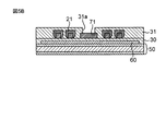
- the thickness of the first spiral wiring 21 and the first sacrificial conductor 71 A difference in thickness occurs. Therefore, as shown in FIG. 5B, when the opening 31a is provided in a part of the first insulating resin 31 covering the first spiral wiring 21 and the first sacrificial conductor 71 to expose the first sacrificial conductor 71, the opening The depth of 31a becomes deep.
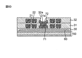
- the second spiral wiring 22 and the second sacrificial conductor 72 are provided as shown in FIG. 5C and the opening 32a is provided in the second insulating resin 32 as shown in FIG.
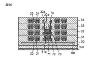
- the depth of the opening 32a is Become deeper. Furthermore, as shown in FIGS. 5E to 5H, as the number of layers increases, the depths of the openings 33a and 34a become deeper, making it difficult to form the openings 33a and 34a. That is, since the openings 31a to 34a of each layer are gradually deepened, it is necessary to shift the focus of the laser in each layer when forming the openings 31a to 34a by laser processing. In addition, it becomes difficult to provide the sacrificial conductors 71 to 74 in the openings 31a to 34a.
- the insulating resins 30 to 34 come into contact with the base 50. Not. Accordingly, it is possible to prevent delamination due to thermal stress caused by a difference in linear expansion coefficient between the base 50 and the insulating resins 30 to 34 at the time of thermal shock or reflow load.
- the coil substrate 5 is formed by laminating the insulating resins 30 to 34 and the spiral wirings 21 to 24 on the base 50, the insulating resin 30 to 34 contracts and the wires of the base 50 and the insulating resins 30 to 34 are formed.
- the processing strain caused by the difference in expansion coefficient can be reduced by making the base 50 thick.
- the coil substrate 5 has a multilayer structure, it is possible to effectively reduce processing distortion and achieve high accuracy.
- the base 50 is peeled off from the coil substrate 5, the coil component 2 can be thinned. Therefore, it is possible to achieve both multilayering and high accuracy without increasing the thickness of the coil component 2.
- the coil component 2 can be composed of the insulating resins 30 to 34 and the spiral wirings 21 to 24, the density of the spiral wirings 21 to 24 can be increased. For this reason, L value can be made high and Rdc can be made low, and high performance can be achieved.
- the coil component has four layers of spiral wiring and five layers of insulating resin.
- the coil component has at least one layer of spiral wiring (first spiral wiring) and at least two layers of insulating resin (base). (Insulating resin, first insulating resin).
- the base has the insulating substrate and the base metal layer, but the base metal layer may be omitted and only the insulating substrate may be provided.
- the coil substrate is formed on one of both surfaces of the base, but the coil substrate may be formed on each of both surfaces of the substrate. Thereby, high productivity can be obtained.
- the dummy metal layer is adhered on the base, but the dummy metal layer may be provided on the base by printing or the like.
- the base is peeled off from the dummy metal layer at the interface between the base and the dummy metal layer.
- the base may be scraped off or the base may be left as it is.
- the sacrificial conductor has the same shape in each layer.
- the inner magnetic path may not be the same shape. Can be obtained.
- the manufacturing method is described by taking an example of an opening for an inner magnetic path that is a magnetic path formed inside the spiral coil.
- the same method is used for an outer magnetic path formed outside the spiral coil. Can be manufactured.
- the first spiral wiring and the first sacrificial conductor are enlarged by plating, but the first spiral wiring may not be enlarged by plating, and only the first sacrificial conductor may be enlarged by plating.
- the first spiral wiring and the first sacrificial conductor are provided in one step, as in the above embodiment. That is, since both the first spiral wiring and the first sacrificial conductor are conductors, they can be formed in one step. Thereby, the total of the tolerance of the position of the hole (sacrificial conductor) for the inner magnetic path with respect to the insulating resin and the tolerance of the position of the spiral wiring with respect to the insulating resin is small.
- the cross-sectional area of the inner magnetic path can be increased, and a higher inductance value can be obtained.
- the first sacrificial conductor connected to the dummy metal layer is energized by plating to enlarge the first sacrificial conductor.
- the gap between the first spiral wiring and the first sacrificial conductor can be made narrower than the resolution of photolithography.
- the inner magnetic path cross-sectional area can be increased and the number of turns of the spiral wiring can be increased, so that a higher inductance value can be obtained.
- the second spiral wiring and the second sacrificial conductor are enlarged by plating.
- the second spiral wiring may not be enlarged by plating, but only the second sacrificial conductor may be enlarged by plating.
- the second spiral wiring and the second sacrificial conductor are provided in one step, as in the above embodiment. That is, since the second spiral wiring and the second sacrificial conductor are both conductors, they can be formed in one step. Thereby, the total of the tolerance of the position of the hole (sacrificial conductor) for the inner magnetic path with respect to the insulating resin and the tolerance of the position of the spiral wiring with respect to the insulating resin is small.
- the cross-sectional area of the inner magnetic path can be increased, and a higher inductance value can be obtained.
- the dummy metal layer is energized to enlarge the second sacrificial conductor by plating through the first sacrificial conductor.
- the gap between the second spiral wiring and the second sacrificial conductor can be made narrower than the resolution of photolithography.
- the inner magnetic path cross-sectional area can be increased and the number of turns of the spiral wiring can be increased, so that a higher inductance value can be obtained.
Landscapes
- Engineering & Computer Science (AREA)
- Power Engineering (AREA)
- Microelectronics & Electronic Packaging (AREA)
- Manufacturing & Machinery (AREA)
- Coils Or Transformers For Communication (AREA)
- Manufacturing Cores, Coils, And Magnets (AREA)
- Production Of Multi-Layered Print Wiring Board (AREA)
- Parts Printed On Printed Circuit Boards (AREA)
Abstract
コイル部品の製造方法は、基台上にダミー金属層を接着する工程と、ダミー金属層上にベース絶縁樹脂を積層する工程と、ベース絶縁樹脂に開口部を設けてダミー金属層を露出させる工程と、ベース絶縁樹脂上に第1スパイラル配線を設け、ベース絶縁樹脂の開口部内のダミー金属層上に第1犠牲導体を設ける工程と、ダミー金属層に通電して第1犠牲導体をめっきにより大きくする工程と、第1スパイラル配線および第1犠牲導体を第1絶縁樹脂で覆う工程と、第1絶縁樹脂に開口部を設けて第1犠牲導体を露出させる工程と、第1絶縁樹脂の開口部から第1犠牲導体をエッチングにより取り除き孔部を形成する工程と、孔部に磁性樹脂を充填して磁性樹脂にて内磁路を構成する工程と、を有する。
Description
本発明は、コイル部品の製造方法に関する。
従来、コイル部品としては、特開2013-225718号公報(特許文献1)に記載されたものがある。このコイル部品の製造方法では、基板に内磁路用の孔部を形成し、その後、基板の上下面にスパイラル配線をフォトリソ等により設ける。
ところで、前記従来のコイル部品を実際に製造しようとすると、次の問題があることを見出した。つまり、基板に対する孔部の位置の公差と、基板に対するスパイラル配線の位置の公差の合計を考慮して、スパイラル配線と孔部との間にある程度の距離が必要となる。これにより、孔部の断面積は、孔部の位置の公差およびスパイラル配線の位置の公差分だけ小さくなる。結果として、内磁路の断面積が小さくなり、高いインダクタンス値を得ることが困難である。
そこで、本発明の課題は、内磁路の断面積を大きくでき、より高いインダクタンス値を得ることができるコイル部品の製造方法を提供することにある。
前記課題を解決するため、本発明の一態様であるコイル部品の製造方法は、
基台上にダミー金属層を設ける工程と、
前記ダミー金属層上にベース絶縁樹脂を積層する工程と、
前記ベース絶縁樹脂に開口部を設けて、前記ダミー金属層を露出させる工程と、
前記ベース絶縁樹脂上に第1スパイラル配線を設け、前記ベース絶縁樹脂の開口部内の前記ダミー金属層上に内磁路に対応する第1犠牲導体を設ける工程と、
前記第1スパイラル配線に直接的または間接的に通電して前記第1スパイラル配線をめっきにより大きくすると共に、前記ダミー金属層に通電して前記ダミー金属層に接続された前記第1犠牲導体をめっきにより大きくする工程と、
前記第1スパイラル配線および前記第1犠牲導体を前記第1絶縁樹脂で覆う工程と、
前記第1絶縁樹脂に開口部を設けて、前記第1犠牲導体を露出させる工程と、
前記第1絶縁樹脂の開口部から前記第1犠牲導体をエッチングにより取り除き、内磁路に対応する孔部を形成する工程と、
前記孔部に磁性樹脂を充填して前記磁性樹脂にて前記内磁路を構成する工程と
を備える。
基台上にダミー金属層を設ける工程と、
前記ダミー金属層上にベース絶縁樹脂を積層する工程と、
前記ベース絶縁樹脂に開口部を設けて、前記ダミー金属層を露出させる工程と、
前記ベース絶縁樹脂上に第1スパイラル配線を設け、前記ベース絶縁樹脂の開口部内の前記ダミー金属層上に内磁路に対応する第1犠牲導体を設ける工程と、
前記第1スパイラル配線に直接的または間接的に通電して前記第1スパイラル配線をめっきにより大きくすると共に、前記ダミー金属層に通電して前記ダミー金属層に接続された前記第1犠牲導体をめっきにより大きくする工程と、
前記第1スパイラル配線および前記第1犠牲導体を前記第1絶縁樹脂で覆う工程と、
前記第1絶縁樹脂に開口部を設けて、前記第1犠牲導体を露出させる工程と、
前記第1絶縁樹脂の開口部から前記第1犠牲導体をエッチングにより取り除き、内磁路に対応する孔部を形成する工程と、
前記孔部に磁性樹脂を充填して前記磁性樹脂にて前記内磁路を構成する工程と
を備える。
本発明の一態様であるコイル部品の製造方法によれば、第1スパイラル配線と第1犠牲導体とを1つの工程で設けている。つまり、第1スパイラル配線と第1犠牲導体は、ともに導体であるから、1つの工程で形成することが可能である。これにより、絶縁樹脂に対する内磁路用の孔部(犠牲導体)の位置の公差と、絶縁樹脂に対するスパイラル配線の位置の公差の合計は、小さい。結果として、内磁路の断面積を大きくでき、より高いインダクタンス値を得ることができる。
また、第1スパイラル配線に直接的または間接的に通電して第1スパイラル配線をめっきにより大きくし、ダミー金属層に通電してダミー金属層に接続された第1犠牲導体をめっきにより大きくする。これにより、第1スパイラル配線の厚さと第1犠牲導体の厚さの差を無くすことができる。したがって、第1スパイラル配線および第1犠牲導体を覆う第1絶縁樹脂に開口部を設けて、第1犠牲導体を露出させるとき、開口部の深さは浅く、開口部の形成は容易となる。
また、コイル部品の製造方法の一実施形態では、
前記第1犠牲導体を露出させる工程と前記孔部を形成する工程との間に、
前記第1絶縁樹脂上に第2スパイラル配線を設け、前記第1絶縁樹脂の開口部内の前記第1犠牲導体上に内磁路に対応する第2犠牲導体を設ける工程と、
前記第2スパイラル配線に直接的または間接的に通電して前記第2スパイラル配線をめっきにより大きくすると共に、前記ダミー金属層に通電して前記第1犠牲導体を介して前記第2犠牲導体をめっきにより大きくする工程と、
前記第2スパイラル配線および前記第2犠牲導体を前記第2絶縁樹脂で覆う工程と、
前記第2絶縁樹脂に開口部を設けて、前記第2犠牲導体を露出させる工程と
を有し、
前記孔部を形成する工程は、前記第2絶縁樹脂の開口部から前記第1犠牲導体および前記第2犠牲導体をエッチングにより取り除き、内磁路に対応する孔部を形成する。
前記第1犠牲導体を露出させる工程と前記孔部を形成する工程との間に、
前記第1絶縁樹脂上に第2スパイラル配線を設け、前記第1絶縁樹脂の開口部内の前記第1犠牲導体上に内磁路に対応する第2犠牲導体を設ける工程と、
前記第2スパイラル配線に直接的または間接的に通電して前記第2スパイラル配線をめっきにより大きくすると共に、前記ダミー金属層に通電して前記第1犠牲導体を介して前記第2犠牲導体をめっきにより大きくする工程と、
前記第2スパイラル配線および前記第2犠牲導体を前記第2絶縁樹脂で覆う工程と、
前記第2絶縁樹脂に開口部を設けて、前記第2犠牲導体を露出させる工程と
を有し、
前記孔部を形成する工程は、前記第2絶縁樹脂の開口部から前記第1犠牲導体および前記第2犠牲導体をエッチングにより取り除き、内磁路に対応する孔部を形成する。
前記実施形態によれば、第2スパイラル配線と第2犠牲導体とを1つの工程で設けている。つまり、第2スパイラル配線と第2犠牲導体は、ともに導体であるから、1つの工程で形成することが可能である。これにより、絶縁樹脂に対する内磁路用の孔部(犠牲導体)の位置の公差と、絶縁樹脂に対するスパイラル配線の位置の公差の合計は、小さい。結果として、内磁路の断面積を大きくでき、より高いインダクタンス値を得ることができる。
また、第2スパイラル配線に直接的または間接的に通電して第2スパイラル配線をめっきにより大きくすると共に、ダミー金属層に通電して第1犠牲導体を介して第2犠牲導体をめっきにより大きくする。これにより、第2スパイラル配線の厚さと第2犠牲導体の厚さの差を無くすことができる。したがって、第2絶縁樹脂に設ける開口部の深さは、第1絶縁樹脂の開口部の深さと同じになる。さらに、多層となっても、開口部の深さは一定となり、開口部の形成は容易となる。また、開口部内に設ける犠牲導体の形状も一定とできる。
また、コイル部品の製造方法の一実施形態では、
前記第1スパイラル配線および前記第1犠牲導体をめっきにより大きくする工程では、前記第1スパイラル配線と前記第1犠牲導体とを同時に通電し、
前記第2スパイラル配線および前記第2犠牲導体をめっきにより大きくする工程では、前記第2スパイラル配線と前記第2犠牲導体とを同時に通電する。
前記第1スパイラル配線および前記第1犠牲導体をめっきにより大きくする工程では、前記第1スパイラル配線と前記第1犠牲導体とを同時に通電し、
前記第2スパイラル配線および前記第2犠牲導体をめっきにより大きくする工程では、前記第2スパイラル配線と前記第2犠牲導体とを同時に通電する。
前記実施形態によれば、第1スパイラル配線と第1犠牲導体とを同時にめっき通電し、第2スパイラル配線と第2犠牲導体とを同時にめっき通電するので、めっきの加工時間を短縮できる。
また、コイル部品の製造方法の一実施形態では、前記ベース絶縁樹脂の開口部と前記第1絶縁樹脂の開口部とは、環状に開口される。
前記実施形態によれば、ベース絶縁樹脂の開口部と第1絶縁樹脂の開口部とは、環状に開口されるので、レーザ加工などによる開口の加工負荷を小さくできる。また、開口部の中央に絶縁樹脂を残しているため、使用する犠牲導体の材料を少なくできる。
また、コイル部品の製造方法の一実施形態では、
前記孔部を形成する工程と前記内磁路を構成する工程との間に、
前記基台と前記ダミー金属層との界面で前記基台を前記ダミー金属層から剥がす工程を有する。
前記孔部を形成する工程と前記内磁路を構成する工程との間に、
前記基台と前記ダミー金属層との界面で前記基台を前記ダミー金属層から剥がす工程を有する。
前記実施形態によれば、基台とダミー金属層との界面で基台をダミー金属層から剥がすので、絶縁樹脂は、基台に接触していない。したがって、熱衝撃やリフロー負荷時に、基台と絶縁樹脂の線膨張係数差によって生じる熱応力による層剥離を防止できる。
また、コイル部品の製造方法の一実施形態では、
基台上にダミー金属層を設ける工程と、
前記ダミー金属層上にベース絶縁樹脂を積層する工程と、
前記ベース絶縁樹脂に開口部を設けて、前記ダミー金属層を露出させる工程と、
前記ベース絶縁樹脂上に第1スパイラル配線を設け、前記ベース絶縁樹脂の開口部内の前記ダミー金属層上に内磁路に対応する第1犠牲導体を設ける工程と、
前記ダミー金属層に通電して前記ダミー金属層に接続された前記第1犠牲導体をめっきにより大きくする工程と、
前記第1スパイラル配線および前記第1犠牲導体を前記第1絶縁樹脂で覆う工程と、
前記第1絶縁樹脂に開口部を設けて、前記第1犠牲導体を露出させる工程と、
前記第1絶縁樹脂の開口部から前記第1犠牲導体をエッチングにより取り除き、内磁路に対応する孔部を形成する工程と、
前記孔部に磁性樹脂を充填して前記磁性樹脂にて前記内磁路を構成する工程と
を備える。
基台上にダミー金属層を設ける工程と、
前記ダミー金属層上にベース絶縁樹脂を積層する工程と、
前記ベース絶縁樹脂に開口部を設けて、前記ダミー金属層を露出させる工程と、
前記ベース絶縁樹脂上に第1スパイラル配線を設け、前記ベース絶縁樹脂の開口部内の前記ダミー金属層上に内磁路に対応する第1犠牲導体を設ける工程と、
前記ダミー金属層に通電して前記ダミー金属層に接続された前記第1犠牲導体をめっきにより大きくする工程と、
前記第1スパイラル配線および前記第1犠牲導体を前記第1絶縁樹脂で覆う工程と、
前記第1絶縁樹脂に開口部を設けて、前記第1犠牲導体を露出させる工程と、
前記第1絶縁樹脂の開口部から前記第1犠牲導体をエッチングにより取り除き、内磁路に対応する孔部を形成する工程と、
前記孔部に磁性樹脂を充填して前記磁性樹脂にて前記内磁路を構成する工程と
を備える。
また、コイル部品の製造方法の一実施形態では、
前記第1犠牲導体を露出させる工程と前記孔部を形成する工程との間に、
前記第1絶縁樹脂上に第2スパイラル配線を設け、前記第1絶縁樹脂の開口部内の前記第1犠牲導体上に内磁路に対応する第2犠牲導体を設ける工程と、
前記ダミー金属層に通電して前記第1犠牲導体を介して前記第2犠牲導体をめっきにより大きくする工程と、
前記第2スパイラル配線および前記第2犠牲導体を前記第2絶縁樹脂で覆う工程と、
前記第2絶縁樹脂に開口部を設けて、前記第2犠牲導体を露出させる工程と
を有し、
前記孔部を形成する工程は、前記第2絶縁樹脂の開口部から前記第1犠牲導体および前記第2犠牲導体をエッチングにより取り除き、内磁路に対応する孔部を形成する。
前記第1犠牲導体を露出させる工程と前記孔部を形成する工程との間に、
前記第1絶縁樹脂上に第2スパイラル配線を設け、前記第1絶縁樹脂の開口部内の前記第1犠牲導体上に内磁路に対応する第2犠牲導体を設ける工程と、
前記ダミー金属層に通電して前記第1犠牲導体を介して前記第2犠牲導体をめっきにより大きくする工程と、
前記第2スパイラル配線および前記第2犠牲導体を前記第2絶縁樹脂で覆う工程と、
前記第2絶縁樹脂に開口部を設けて、前記第2犠牲導体を露出させる工程と
を有し、
前記孔部を形成する工程は、前記第2絶縁樹脂の開口部から前記第1犠牲導体および前記第2犠牲導体をエッチングにより取り除き、内磁路に対応する孔部を形成する。
本発明のコイル部品の製造方法によれば、第1スパイラル配線と第1犠牲導体とを1つの工程で設けているので、内磁路の断面積を大きくでき、より高いインダクタンス値を得ることができる。
以下、本発明を図示の実施の形態により詳細に説明する。
図1は、本発明のコイル部品の一実施形態を含む電子部品を示す分解斜視図である。図2は、コイル部品の断面図である。図1に示すように、電子部品1は、例えば、パソコン、DVDプレーヤー、デジカメ、TV、携帯電話、カーエレクトロニクスなどの電子機器に搭載される。電子部品1は、並列に配置された2つのコイル部品2を有する。
図1と図2に示すように、コイル部品2は、4層のスパイラル配線21~24と、4層のスパイラル配線21~24をそれぞれ覆う絶縁樹脂体35と、絶縁樹脂体35を覆う磁性樹脂40とを有する。この明細書において、対象物を覆うとは、対象物の少なくとも一部を覆うことをいう。図1では、絶縁樹脂体35を省略して描いている。
第1から第4スパイラル配線21~24は、下層から上層に順に、配置される。第1から第4スパイラル配線21~24は、それぞれ、平面においてスパイラル状に形成されている。第1から第4スパイラル配線21~24は、例えば、Cu、Ag、Auなどの低抵抗な金属によって構成される。好ましくは、セミアディティブ工法によって形成されるCuめっきを用いることで、低抵抗でかつ狭ピッチなスパイラル配線を形成できる。
絶縁樹脂体35は、ベース絶縁樹脂30および第1から第4絶縁樹脂31~34を有する。ベース絶縁樹脂30および第1から第4絶縁樹脂31~34は、下層から上層に順に、配置される。絶縁樹脂30~34の材料は、例えば、エポキシ系樹脂やビスマレイミド、液晶ポリマ、ポリイミドなどからなる有機絶縁材料の単独材料もしくは、シリカフィラーなどの無機フィラー材料や、ゴム系材料からなる有機系フィラーなどとの組み合わせからなる絶縁材料である。好ましくは、全ての絶縁樹脂30~34は、同一材料で構成される。この実施形態では、全ての絶縁樹脂30~34は、シリカフィラーを含有したエポキシ樹脂で構成される。
第1スパイラル配線21は、ベース絶縁樹脂30上に積層される。第1絶縁樹脂31は、第1スパイラル配線21に積層され、第1スパイラル配線21を覆う。第2スパイラル配線22は、第1絶縁樹脂31上に積層される。第2絶縁樹脂32は、第2スパイラル配線22に積層され、第2スパイラル配線22を覆う。
第3スパイラル配線23は、第2絶縁樹脂32上に積層される。第3絶縁樹脂33は、第3スパイラル配線23に積層され、第3スパイラル配線23を覆う。第4スパイラル配線24は、第3絶縁樹脂33上に積層される。第4絶縁樹脂34は、第4スパイラル配線24に積層され、第4スパイラル配線24を覆う。
第2スパイラル配線22は、積層方向に延在するビア配線25を介して、第1スパイラル配線21に接続される。ビア配線25は、第1絶縁樹脂31に設けられる。第1スパイラル配線21の内周端21aと第2スパイラル配線22の内周端22aとは、ビア配線25を介して、接続される。第1スパイラル配線21の外周端21bは、図示しない外部電極に接続される。第2スパイラル配線22の外周端22bは、図示しない外部電極に接続される。
第4スパイラル配線24は、積層方向に延在するビア配線26を介して、第3スパイラル配線23に接続される。ビア配線26は、第3絶縁樹脂33に設けられる。第3スパイラル配線23の内周端23aと第4スパイラル配線24の内周端24aとは、ビア配線26を介して、接続される。第3スパイラル配線23の外周端23bは、図示しない外部電極に接続される。第4スパイラル配線24の外周端24bは、図示しない外部電極に接続される。
第1から第4スパイラル配線21~24は、同一軸を中心として、配置されている。第1スパイラル配線21と第2スパイラル配線22とは、軸方向(積層方向)からみて、同一方向に巻き回されている。第3スパイラル配線23と第4スパイラル配線24とは、軸方向からみて、同一方向に巻き回されている。第1、第2スパイラル配線21,22と第3、第4スパイラル配線23,24とは、軸方向からみて、互いに逆方向に巻き回されている。
第1から第4スパイラル配線21~24の内面および外面は、絶縁樹脂体35に覆われている。絶縁樹脂体35は、第1から第4スパイラル配線21~24の同一軸を中心とした孔部35aを有する。
磁性樹脂40は、絶縁樹脂体35を覆う。磁性樹脂40は、絶縁樹脂体35の孔部35aに設けられた内部分41と、絶縁樹脂体35の外部(外周面および上下端面)に設けられた外部分42とを有する。内部分41は、コイル部品2の内磁路を構成し、外部分42は、コイル部品2の外磁路を構成する。
磁性樹脂40の材料は、例えば、磁性体粉含有の樹脂材料である。磁性体粉は、例えば、Fe、Si、Cr等の金属磁性材料であり、樹脂材料は、例えば、エポキシ等の樹脂材料である。コイル部品2の特性(L値および重畳特性)を向上させるため、磁性体粉は、90wt%以上含有されていることが望ましく、また、磁性樹脂40の充填性を向上させるため、粒度分布の異なる2または3種類の磁性体粉を混在させるとさらによい。
次に、コイル部品2の製造方法について説明する。
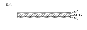
図3Aに示すように、基台50を準備する。基台50は、絶縁基板51と、絶縁基板51の両面に設けられたベース金属層52とを有する。この実施形態では、絶縁基板51は、ガラスエポキシ基板であり、ベース金属層52は、Cu箔である。
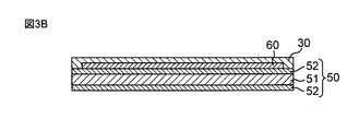
そして、図3Bに示すように、基台50上にダミー金属層60を接着する。この実施形態では、ダミー金属層60は、Cu箔である。ダミー金属層60は、基台50のベース金属層52と接着されるので、ダミー金属層60は、ベース金属層52の円滑面に接着される。このため、ダミー金属層60とベース金属層52の接着力を弱くすることができて、後工程において、基台50をダミー金属層60から容易に剥がすことができる。好ましくは、基台50とダミー金属層60を接着する接着剤は、低粘着接着剤とする。また、基台50とダミー金属層60の接着力を弱くするために、基台50とダミー金属層60の界面を光沢面とすることが望ましい。
その後、基台50に仮止めされたダミー金属層60上にベース絶縁樹脂30を積層する。このとき、ベース絶縁樹脂30を真空ラミネータにより積層してから熱硬化する。
そして、図3Cに示すように、ベース絶縁樹脂30の一部に開口部30aを設けて、ダミー金属層60を露出させる。開口部30aは、レーザ加工により形成される。
そして、図3Dに示すように、ベース絶縁樹脂30上に第1スパイラル配線21を設け、ベース絶縁樹脂30の開口部30a内のダミー金属層60上に内磁路に対応する第1犠牲導体71を設ける。このとき、第1スパイラル配線21および第1犠牲導体71を、SAP(Semi Additive Process)により、同時に形成する。
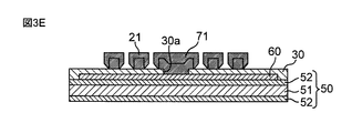
そして、図3Eに示すように、第1スパイラル配線21に間接的に通電して第1スパイラル配線21をめっきにより大きくすると共に、ダミー金属層60に通電してダミー金属層60に接続された第1犠牲導体71をめっきにより大きくする。これにより、低抵抗でかつ狭ピッチなスパイラル配線を形成できる。このとき、第1スパイラル配線21を図示しない配線パターンに接続することで、配線パターンを介して第1スパイラル配線21に間接的に通電する。なお、第1スパイラル配線21に直接的に通電するようにしてもよい。第1スパイラル配線21および第1犠牲導体71を同時に形成してもよく、加工時間を短縮できる。
そして、図3Fに示すように、第1スパイラル配線21および第1犠牲導体71を第1絶縁樹脂31で覆う。このとき、第1絶縁樹脂31を真空ラミネータで積層してから熱硬化する。その後、第1絶縁樹脂31に、レーザ加工により、ビア配線25を充填するためのビアホールを形成する。
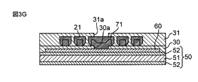
そして、図3Gに示すように、第1絶縁樹脂31の一部に開口部31aを設けて、第1犠牲導体71を露出させる。開口部31aは、レーザ加工により形成される。
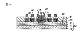
そして、図3Hに示すように、第1絶縁樹脂31上に第2スパイラル配線22を設け、第1絶縁樹脂31の開口部31a内の第1犠牲導体71上に内磁路に対応する第2犠牲導体72を設ける。なお、2層目以降の処理は、1層目の処理と同様である。
そして、図3Iに示すように、第2スパイラル配線22に直接的または間接的に通電して第2スパイラル配線22をめっきにより大きくすると共に、ダミー金属層60に通電して第1犠牲導体71を介して第2犠牲導体72をめっきにより大きくする。
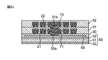
そして、図3Jに示すように、第2スパイラル配線22および第2犠牲導体72を第2絶縁樹脂32で覆う。このとき、第2絶縁樹脂32を第1絶縁樹脂31と同様の処理にて設ける。
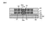
そして、図3Kに示すように、第2絶縁樹脂32の一部に開口部32aを設けて、第2犠牲導体72を露出させる。開口部32aは、レーザ加工により形成される。
そして、図3Lに示すように、2層目と同様の処理を行って、3層目の第3スパイラル配線23、第3犠牲導体73および第3絶縁樹脂33と、4層目の第4スパイラル配線24、第4犠牲導体74および第4絶縁樹脂34とを設ける。第3犠牲導体73は、ダミー金属層60に通電することで、第1、第2犠牲導体71,72を介して通電されて、めっきにより大きくなる。第4犠牲導体74は、ダミー金属層60に通電することで、第1~第3犠牲導体71~73を介して通電されて、めっきにより大きくなる。第3絶縁樹脂33に、レーザ加工により、ビア配線26を充填するためのビアホールを形成する。
そして、図3Mに示すように、第4絶縁樹脂34の一部に開口部34aを設けて、第4犠牲導体74を露出させる。
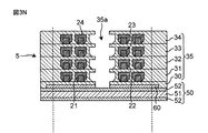
そして、図3Nに示すように、第4絶縁樹脂34の開口部34aから第1から第4犠牲導体71~74をエッチングにより取り除き、スパイラル配線21~24および絶縁樹脂30~34で構成される絶縁樹脂体35に、内磁路に対応する孔部35aを形成する。犠牲導体71~74の材料は、例えば、スパイラル配線21~24の材料と同じである。このようにして、スパイラル配線21~24および絶縁樹脂30~34により、コイル基板5を形成する。
そして、図3Oに示すように、コイル基板5の端部を基台50の端部とともにカットライン10で切り落とす。カットライン10は、ダミー金属層60の端面よりも内側に位置する。
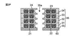
そして、図3Pに示すように、基台50(ベース金属層52)の一面とダミー金属層60との界面で基台50をダミー金属層60から剥がす。
そして、図3Qに示すように、ダミー金属層60をコイル基板5から取り除く。このとき、ダミー金属層60をエッチングにより取り除く。第1から第4スパイラル配線21~24は、ベース絶縁樹脂30および第1から第4絶縁樹脂31~34で構成される絶縁樹脂体35により、覆われる。
そして、図3Rに示すように、コイル基板5を磁性樹脂40で覆う。このとき、コイル基板5の積層方向の両側に、シート状に成形した磁性樹脂40を複数枚配置し、真空ラミネータもしくは真空プレス機により、加熱圧着させ、その後硬化処理をする。磁性樹脂40は、絶縁樹脂体35の孔部35aに充填されて内磁路を構成し、絶縁樹脂体35の外部に設けられて外磁路を構成する。そして、スパイラル配線21~24の端部に(図示しない)外部端子を接続して、コイル部品2を形成する。
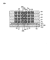
なお、図3Mに示すように、ベース絶縁樹脂30の開口部30aと、第1絶縁樹脂31の開口部31aと、第2絶縁樹脂32の開口部32aと、第3絶縁樹脂33の開口部33aとは、全開口されているが、図4に示すように、ベース絶縁樹脂30の開口部30bと、第1絶縁樹脂31の開口部31bと、第2絶縁樹脂32の開口部32bと、第3絶縁樹脂33の開口部33bとは、環状に開口されるようにしてもよい。これにより、レーザ加工などによる開口の加工負荷を小さくできる。また、開口部の中央に絶縁樹脂を残しているため、使用する犠牲導体の材料を少なくできる。
前記コイル部品2の製造方法によれば、第1スパイラル配線21と第1犠牲導体71とを1つの工程で設けている。つまり、第1スパイラル配線21と第1犠牲導体71は、ともに導体であるから、1つの工程で形成することが可能である。なお、第2から第4スパイラル配線22~24および第2から第4犠牲導体72~74を設ける場合についても同様である。これにより、絶縁樹脂30~34に対する内磁路用の孔部35a(犠牲導体71~74)の位置の公差と、絶縁樹脂30~34に対するスパイラル配線21~24の位置の公差の合計は、小さい。結果として、内磁路の断面積を大きくでき、より高いインダクタンス値を得ることができる。
これに対して、従来に示すように、絶縁樹脂に内磁路用の孔部を形成する工程と、絶縁樹脂にスパイラル配線を形成する工程とを、別の工程で行う場合、絶縁樹脂に対する孔部の位置の公差と、絶縁樹脂に対するスパイラル配線の位置の公差の合計を考慮して、スパイラル配線と孔部との間にある程度の距離が必要となる。これにより、孔部の断面積は、孔部の位置の公差およびスパイラル配線の位置の公差分だけ小さくなる。結果として、内磁路の断面積が小さくなり、高いインダクタンス値を得ることが困難である。
また、第1スパイラル配線21に直接的または間接的に通電して第1スパイラル配線21をめっきにより大きくし、ダミー金属層60に通電してダミー金属層60に接続された第1犠牲導体71をめっきにより大きくする。これにより、第1スパイラル配線21の厚さと第1犠牲導体71の厚さの差を無くすことができる。したがって、第1スパイラル配線21および第1犠牲導体71を覆う第1絶縁樹脂31の一部に開口部31aを設けて、第1犠牲導体71を露出させるとき、開口部31aの深さは浅く、開口部31aの形成は容易となる。
そして、第2スパイラル配線22に直接的または間接的に通電して第2スパイラル配線22をめっきにより大きくすると共に、ダミー金属層60に通電して第1犠牲導体71を介して第2犠牲導体72をめっきにより大きくする。これにより、第2スパイラル配線22の厚さと第2犠牲導体72の厚さの差を無くすことができる。したがって、第2絶縁樹脂32に設ける開口部32aの深さは、第1絶縁樹脂31の開口部31aの深さと同じになる。さらに、多層となっても、開口部31a~34aの深さは一定となり、開口部31a~34aの形成は容易となる。また、開口部31a~34a内に設ける犠牲導体71~74の形状も一定とできる。
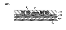
これに対して、図5Aに示すように、第1スパイラル配線21をめっきにより大きくする一方、第1犠牲導体71をめっきにより大きくしない場合、第1スパイラル配線21の厚さと第1犠牲導体71の厚さの差が生じる。したがって、図5Bに示すように、第1スパイラル配線21および第1犠牲導体71を覆う第1絶縁樹脂31の一部に開口部31aを設けて、第1犠牲導体71を露出させるとき、開口部31aの深さは深くなる。特に、図5Cに示すように、第2スパイラル配線22および第2犠牲導体72を設け、図5Dに示すように、第2絶縁樹脂32に開口部32aを設ける場合、開口部32aの深さが一層深くなる。さらに、図5E~図5Hに示すように、多層となるほど、開口部33a,34aの深さが一層深くなって、開口部33a,34aの形成が困難となる。つまり、各層の開口部31a~34aは次第に深くなるため、レーザ加工により開口部31a~34aを形成するとき、各層でレーザの焦点をずらす必要がある。また、犠牲導体71~74を開口部31a~34a内に設けることも困難となる。
前記コイル部品2の製造方法によれば、基台50の一面とダミー金属層60との界面で基台50をダミー金属層60から剥がすので、絶縁樹脂30~34は、基台50に接触していない。したがって、熱衝撃やリフロー負荷時に、基台50と絶縁樹脂30~34の線膨張係数差によって生じる熱応力による層剥離を防止できる。
また、基台50上に絶縁樹脂30~34とスパイラル配線21~24を積層してコイル基板5を形成するので、絶縁樹脂30~34の収縮や、基台50と絶縁樹脂30~34の線膨張係数差によって生じる加工歪を、基台50を厚くすることで、低減することができる。特に、コイル基板5を多層とする場合に、加工歪みを有効に低減して、高精度化を実現できる。その後、基台50をコイル基板5から剥がしているので、コイル部品2の薄型が可能となる。したがって、コイル部品2を厚くすることなく、多層化と高精度化を両立できる。
また、コイル部品2を絶縁樹脂30~34およびスパイラル配線21~24で構成できるため、スパイラル配線21~24の密度を高くすることができる。このため、L値を高くでき、かつ、Rdcを低くできて、高性能化を図ることができる。
また、全ての絶縁樹脂30~34は、同一材料で構成されるので、各絶縁樹脂30~34の線膨張係数の差をなくし、熱衝撃やリフロー負荷時に、各絶縁樹脂30~34の層剥離を防止できる。
なお、本発明は上述の実施形態に限定されず、本発明の要旨を逸脱しない範囲で設計変更可能である。
前記実施形態では、コイル部品は、4層のスパイラル配線と5層の絶縁樹脂とを有しているが、少なくとも1層のスパイラル配線(第1スパイラル配線)と、少なくとも2層の絶縁樹脂(ベース絶縁樹脂、第1絶縁樹脂)とを有していればよい。
前記実施形態では、基台は、絶縁基板とベース金属層とを有するようにしているが、ベース金属層を省略して絶縁基板のみを有するようにしてもよい。
前記実施形態では、基台の両面のうちの一面にコイル基板を形成しているが、基板の両面のそれぞれにコイル基板を形成するようにしてもよい。これにより、高い生産性を得ることができる。
前記実施形態では、基台上にダミー金属層を接着しているが、基台上にダミー金属層を印刷等により設けるようにしてもよい。
前記実施形態では、基台とダミー金属層との界面で基台をダミー金属層から剥がしているが、基台を削り取るようにしてもよく、または、基台をそのまま残しておいてもよい。
前記実施形態では、犠牲導体の形状が各層で同一形状の場合を示しているが、本製造方法では、犠牲導体の一部が各層間で接続できていれば、同一形状でなくとも内磁路に対応する開口を得ることができる。
前記実施形態では、スパイラルコイルの内側に形成する磁路である内磁路に対する開口を例に製造方法を記述しているが、スパイラルコイルの外側に形成する外磁路に対しても同じ方法で製造することができる。
前記実施形態では、第1スパイラル配線と第1犠牲導体をめっきにより大きくしているが、第1スパイラル配線はめっきにより大きくせずに、第1犠牲導体のみをめっきにより大きくしてもよい。
上記の製造方法であっても、前記実施形態と同様に、第1スパイラル配線と第1犠牲導体とを1つの工程で設けている。つまり、第1スパイラル配線と第1犠牲導体は、ともに導体であるから、1つの工程で形成することが可能である。これにより、絶縁樹脂に対する内磁路用の孔部(犠牲導体)の位置の公差と、絶縁樹脂に対するスパイラル配線の位置の公差の合計は、小さい。結果として、内磁路の断面積を大きくでき、より高いインダクタンス値を得ることができる。
また、前記実施形態と同様に、ダミー金属層に通電してダミー金属層に接続された第1犠牲導体をめっきにより大きくする。これにより、第1スパイラル配線と第1犠牲導体間のギャップをフォトリソグラフィの解像度以上に狭くすることが出来る。結果として、前記実施形態と同様に、内磁路断面積を大きくでき、スパイラル配線のターン数を大きくできるので、より高いインダクタンス値を得ることが出来る。
上記の製造方法であっても、前記実施形態と同様に、第1スパイラル配線と第1犠牲導体とを1つの工程で設けている。つまり、第1スパイラル配線と第1犠牲導体は、ともに導体であるから、1つの工程で形成することが可能である。これにより、絶縁樹脂に対する内磁路用の孔部(犠牲導体)の位置の公差と、絶縁樹脂に対するスパイラル配線の位置の公差の合計は、小さい。結果として、内磁路の断面積を大きくでき、より高いインダクタンス値を得ることができる。
また、前記実施形態と同様に、ダミー金属層に通電してダミー金属層に接続された第1犠牲導体をめっきにより大きくする。これにより、第1スパイラル配線と第1犠牲導体間のギャップをフォトリソグラフィの解像度以上に狭くすることが出来る。結果として、前記実施形態と同様に、内磁路断面積を大きくでき、スパイラル配線のターン数を大きくできるので、より高いインダクタンス値を得ることが出来る。
前記実施形態では、第2スパイラル配線と第2犠牲導体をめっきにより大きくしているが、第2スパイラル配線はめっきにより大きくせずに、第2犠牲導体のみをめっきにより大きくしてもよい。
上記の製造方法であっても、前記実施形態と同様に、第2スパイラル配線と第2犠牲導体とを1つの工程で設けている。つまり、第2スパイラル配線と第2犠牲導体は、ともに導体であるから、1つの工程で形成することが可能である。これにより、絶縁樹脂に対する内磁路用の孔部(犠牲導体)の位置の公差と、絶縁樹脂に対するスパイラル配線の位置の公差の合計は、小さい。結果として、内磁路の断面積を大きくでき、より高いインダクタンス値を得ることができる。
また、前記実施形態と同様に、ダミー金属層に通電して第1犠牲導体を介して第2犠牲導体をめっきにより大きくする。これにより、第2スパイラル配線と第2犠牲導体間のギャップをフォトリソグラフィの解像度以上に狭くすることが出来る。結果として、前記実施形態と同様に、内磁路断面積を大きくでき、スパイラル配線のターン数を大きくできるので、より高いインダクタンス値を得ることが出来る。
上記の製造方法であっても、前記実施形態と同様に、第2スパイラル配線と第2犠牲導体とを1つの工程で設けている。つまり、第2スパイラル配線と第2犠牲導体は、ともに導体であるから、1つの工程で形成することが可能である。これにより、絶縁樹脂に対する内磁路用の孔部(犠牲導体)の位置の公差と、絶縁樹脂に対するスパイラル配線の位置の公差の合計は、小さい。結果として、内磁路の断面積を大きくでき、より高いインダクタンス値を得ることができる。
また、前記実施形態と同様に、ダミー金属層に通電して第1犠牲導体を介して第2犠牲導体をめっきにより大きくする。これにより、第2スパイラル配線と第2犠牲導体間のギャップをフォトリソグラフィの解像度以上に狭くすることが出来る。結果として、前記実施形態と同様に、内磁路断面積を大きくでき、スパイラル配線のターン数を大きくできるので、より高いインダクタンス値を得ることが出来る。
1 電子部品
2 コイル部品
5 コイル基板
10 カットライン
21~24 第1~第4スパイラル配線
25,26 ビア配線
30 ベース絶縁樹脂
31~34 第1~第4絶縁樹脂
30a~34a,30b~33b 開口部
35 絶縁樹脂体
35a 孔部
40 磁性樹脂
50 基台
51 絶縁基板
52 ベース金属層
60 ダミー金属層
71~74 第1~第4犠牲導体
2 コイル部品
5 コイル基板
10 カットライン
21~24 第1~第4スパイラル配線
25,26 ビア配線
30 ベース絶縁樹脂
31~34 第1~第4絶縁樹脂
30a~34a,30b~33b 開口部
35 絶縁樹脂体
35a 孔部
40 磁性樹脂
50 基台
51 絶縁基板
52 ベース金属層
60 ダミー金属層
71~74 第1~第4犠牲導体
Claims (8)
- 基台上にダミー金属層を設ける工程と、
前記ダミー金属層上にベース絶縁樹脂を積層する工程と、
前記ベース絶縁樹脂に開口部を設けて、前記ダミー金属層を露出させる工程と、
前記ベース絶縁樹脂上に第1スパイラル配線を設け、前記ベース絶縁樹脂の開口部内の前記ダミー金属層上に内磁路に対応する第1犠牲導体を設ける工程と、
前記ダミー金属層に通電して前記ダミー金属層に接続された前記第1犠牲導体をめっきにより大きくする工程と、
前記第1スパイラル配線および前記第1犠牲導体を前記第1絶縁樹脂で覆う工程と、
前記第1絶縁樹脂に開口部を設けて、前記第1犠牲導体を露出させる工程と、
前記第1絶縁樹脂の開口部から前記第1犠牲導体をエッチングにより取り除き、内磁路に対応する孔部を形成する工程と、
前記孔部に磁性樹脂を充填して前記磁性樹脂にて前記内磁路を構成する工程と
を備える、コイル部品の製造方法。 - 前記第1犠牲導体をめっきにより大きくする工程では、
前記第1スパイラル配線に直接的または間接的に通電して前記第1スパイラル配線をめっきにより大きくすると共に、前記ダミー金属層に通電して前記ダミー金属層に接続された前記第1犠牲導体をめっきにより大きくする、請求項1に記載のコイル部品の製造方法。 - 前記第1犠牲導体を露出させる工程と前記孔部を形成する工程との間に、
前記第1絶縁樹脂上に第2スパイラル配線を設け、前記第1絶縁樹脂の開口部内の前記第1犠牲導体上に内磁路に対応する第2犠牲導体を設ける工程と、
前記ダミー金属層に通電して前記第1犠牲導体を介して前記第2犠牲導体をめっきにより大きくする工程と、
前記第2スパイラル配線および前記第2犠牲導体を前記第2絶縁樹脂で覆う工程と、
前記第2絶縁樹脂に開口部を設けて、前記第2犠牲導体を露出させる工程と
を有し、
前記孔部を形成する工程は、前記第2絶縁樹脂の開口部から前記第1犠牲導体および前記第2犠牲導体をエッチングにより取り除き、内磁路に対応する孔部を形成する、請求項1または2に記載のコイル部品の製造方法。 - 前記第2犠牲導体をめっきにより大きくする工程では、
前記第2スパイラル配線に直接的または間接的に通電して前記第2スパイラル配線をめっきにより大きくすると共に、前記ダミー金属層に通電して前記第1犠牲導体を介して前記第2犠牲導体をめっきにより大きくする、請求項3に記載のコイル部品の製造方法。 - 前記第1犠牲導体を露出させる工程と前記孔部を形成する工程との間に、
前記第1絶縁樹脂上に第2スパイラル配線を設け、前記第1絶縁樹脂の開口部内の前記第1犠牲導体上に内磁路に対応する第2犠牲導体を設ける工程と、
前記第2スパイラル配線に直接的または間接的に通電して前記第2スパイラル配線をめっきにより大きくすると共に、前記ダミー金属層に通電して前記第1犠牲導体を介して前記第2犠牲導体をめっきにより大きくする工程と、
前記第2スパイラル配線および前記第2犠牲導体を前記第2絶縁樹脂で覆う工程と、
前記第2絶縁樹脂に開口部を設けて、前記第2犠牲導体を露出させる工程と
を有し、
前記孔部を形成する工程は、前記第2絶縁樹脂の開口部から前記第1犠牲導体および前記第2犠牲導体をエッチングにより取り除き、内磁路に対応する孔部を形成する、請求項2に記載のコイル部品の製造方法。 - 前記第1スパイラル配線および前記第1犠牲導体をめっきにより大きくする工程では、前記第1スパイラル配線と前記第1犠牲導体とを同時に通電し、
前記第2スパイラル配線および前記第2犠牲導体をめっきにより大きくする工程では、前記第2スパイラル配線と前記第2犠牲導体とを同時に通電する、請求項5に記載のコイル部品の製造方法。 - 前記ベース絶縁樹脂の開口部と前記第1絶縁樹脂の開口部とは、環状に開口される、請求項3から6の何れか一つに記載のコイル部品の製造方法。
- 前記孔部を形成する工程と前記内磁路を構成する工程との間に、
前記基台と前記ダミー金属層との界面で前記基台を前記ダミー金属層から剥がす工程を有する、請求項1から7の何れか一つに記載のコイル部品の製造方法。
Priority Applications (3)
| Application Number | Priority Date | Filing Date | Title |
|---|---|---|---|
| JP2017524752A JP6525054B2 (ja) | 2015-06-24 | 2016-05-23 | コイル部品の製造方法 |
| CN201680026501.4A CN107533916B (zh) | 2015-06-24 | 2016-05-23 | 线圈部件的制造方法 |
| US15/846,742 US10515758B2 (en) | 2015-06-24 | 2017-12-19 | Method of manufacturing coil component |
Applications Claiming Priority (2)
| Application Number | Priority Date | Filing Date | Title |
|---|---|---|---|
| JP2015126923 | 2015-06-24 | ||
| JP2015-126923 | 2015-06-24 |
Related Child Applications (1)
| Application Number | Title | Priority Date | Filing Date |
|---|---|---|---|
| US15/846,742 Continuation US10515758B2 (en) | 2015-06-24 | 2017-12-19 | Method of manufacturing coil component |
Publications (1)
| Publication Number | Publication Date |
|---|---|
| WO2016208305A1 true WO2016208305A1 (ja) | 2016-12-29 |
Family
ID=57584820
Family Applications (1)
| Application Number | Title | Priority Date | Filing Date |
|---|---|---|---|
| PCT/JP2016/065172 Ceased WO2016208305A1 (ja) | 2015-06-24 | 2016-05-23 | コイル部品の製造方法 |
Country Status (4)
| Country | Link |
|---|---|
| US (1) | US10515758B2 (ja) |
| JP (1) | JP6525054B2 (ja) |
| CN (1) | CN107533916B (ja) |
| WO (1) | WO2016208305A1 (ja) |
Cited By (5)
| Publication number | Priority date | Publication date | Assignee | Title |
|---|---|---|---|---|
| US20180233279A1 (en) * | 2015-06-24 | 2018-08-16 | Murata Manufacturing Co., Ltd. | Manufacture method of coil component, and coil component |
| JP2018182222A (ja) * | 2017-04-20 | 2018-11-15 | 株式会社村田製作所 | プリント配線基板およびスイッチングレギュレータ |
| JP2019134141A (ja) * | 2018-02-02 | 2019-08-08 | 株式会社村田製作所 | インダクタ部品およびその製造方法 |
| WO2021079697A1 (ja) * | 2019-10-23 | 2021-04-29 | Tdk株式会社 | コイル部品及びその製造方法 |
| JP2021077897A (ja) * | 2018-02-02 | 2021-05-20 | 株式会社村田製作所 | インダクタ部品およびその製造方法 |
Families Citing this family (5)
| Publication number | Priority date | Publication date | Assignee | Title |
|---|---|---|---|---|
| KR102178528B1 (ko) * | 2019-06-21 | 2020-11-13 | 삼성전기주식회사 | 코일 전자부품 |
| KR102253471B1 (ko) * | 2020-01-21 | 2021-05-18 | 삼성전기주식회사 | 코일 부품 |
| US11935678B2 (en) * | 2020-12-10 | 2024-03-19 | GLOBALFOUNDARIES Singapore Pte. Ltd. | Inductive devices and methods of fabricating inductive devices |
| JP7405108B2 (ja) * | 2021-03-17 | 2023-12-26 | 株式会社村田製作所 | インダクタ部品およびその製造方法 |
| TWI842521B (zh) * | 2023-05-10 | 2024-05-11 | 欣興電子股份有限公司 | 線路板結構及其製造方法 |
Citations (4)
| Publication number | Priority date | Publication date | Assignee | Title |
|---|---|---|---|---|
| JPH10290544A (ja) * | 1997-04-14 | 1998-10-27 | S M C:Kk | 厚膜プリントコイルおよびその製造方法 |
| JP2007227729A (ja) * | 2006-02-24 | 2007-09-06 | Matsushita Electric Ind Co Ltd | インダクタンス部品 |
| JP2010171170A (ja) * | 2009-01-22 | 2010-08-05 | Hitachi Cable Ltd | 銅回路配線基板およびその製造方法 |
| JP2016072407A (ja) * | 2014-09-30 | 2016-05-09 | 株式会社村田製作所 | 電子部品の製造方法 |
Family Cites Families (9)
| Publication number | Priority date | Publication date | Assignee | Title |
|---|---|---|---|---|
| JPH11181593A (ja) * | 1997-12-16 | 1999-07-06 | Totoku Electric Co Ltd | 銅被覆アルミニウム線の製造方法 |
| JP4293603B2 (ja) * | 2004-02-25 | 2009-07-08 | Tdk株式会社 | コイル部品及びその製造方法 |
| JP2006278912A (ja) * | 2005-03-30 | 2006-10-12 | Tdk Corp | コイル部品 |
| JP5831498B2 (ja) * | 2013-05-22 | 2015-12-09 | Tdk株式会社 | コイル部品およびその製造方法 |
| JP5614479B2 (ja) | 2013-08-09 | 2014-10-29 | Tdk株式会社 | コイル部品の製造方法 |
| KR101627128B1 (ko) * | 2014-12-02 | 2016-06-13 | 삼성전기주식회사 | 코일 부품 |
| KR101630083B1 (ko) * | 2014-12-03 | 2016-06-13 | 삼성전기주식회사 | 코일 부품 |
| JP6500635B2 (ja) * | 2015-06-24 | 2019-04-17 | 株式会社村田製作所 | コイル部品の製造方法およびコイル部品 |
| JP6354683B2 (ja) * | 2015-07-03 | 2018-07-11 | 株式会社村田製作所 | コイル部品 |
-
2016
- 2016-05-23 JP JP2017524752A patent/JP6525054B2/ja active Active
- 2016-05-23 WO PCT/JP2016/065172 patent/WO2016208305A1/ja not_active Ceased
- 2016-05-23 CN CN201680026501.4A patent/CN107533916B/zh active Active
-
2017
- 2017-12-19 US US15/846,742 patent/US10515758B2/en active Active
Patent Citations (4)
| Publication number | Priority date | Publication date | Assignee | Title |
|---|---|---|---|---|
| JPH10290544A (ja) * | 1997-04-14 | 1998-10-27 | S M C:Kk | 厚膜プリントコイルおよびその製造方法 |
| JP2007227729A (ja) * | 2006-02-24 | 2007-09-06 | Matsushita Electric Ind Co Ltd | インダクタンス部品 |
| JP2010171170A (ja) * | 2009-01-22 | 2010-08-05 | Hitachi Cable Ltd | 銅回路配線基板およびその製造方法 |
| JP2016072407A (ja) * | 2014-09-30 | 2016-05-09 | 株式会社村田製作所 | 電子部品の製造方法 |
Cited By (13)
| Publication number | Priority date | Publication date | Assignee | Title |
|---|---|---|---|---|
| US10600565B2 (en) * | 2015-06-24 | 2020-03-24 | Murata Manufacturing Co., Ltd. | Manufacture method of coil component, and coil component |
| US20180233279A1 (en) * | 2015-06-24 | 2018-08-16 | Murata Manufacturing Co., Ltd. | Manufacture method of coil component, and coil component |
| JP2018182222A (ja) * | 2017-04-20 | 2018-11-15 | 株式会社村田製作所 | プリント配線基板およびスイッチングレギュレータ |
| JP2021077897A (ja) * | 2018-02-02 | 2021-05-20 | 株式会社村田製作所 | インダクタ部品およびその製造方法 |
| JP2019134141A (ja) * | 2018-02-02 | 2019-08-08 | 株式会社村田製作所 | インダクタ部品およびその製造方法 |
| WO2021079697A1 (ja) * | 2019-10-23 | 2021-04-29 | Tdk株式会社 | コイル部品及びその製造方法 |
| JP2021068805A (ja) * | 2019-10-23 | 2021-04-30 | Tdk株式会社 | コイル部品及びその製造方法 |
| CN114568034A (zh) * | 2019-10-23 | 2022-05-31 | Tdk株式会社 | 线圈部件及其制造方法 |
| JP7362416B2 (ja) | 2019-10-23 | 2023-10-17 | Tdk株式会社 | コイル部品及びその製造方法 |
| JP2023168523A (ja) * | 2019-10-23 | 2023-11-24 | Tdk株式会社 | コイル部品 |
| JP7557592B2 (ja) | 2019-10-23 | 2024-09-27 | Tdk株式会社 | コイル部品 |
| US12340937B2 (en) | 2019-10-23 | 2025-06-24 | Tdk Corporation | Coil component and manufacturing method therefor |
| CN114568034B (zh) * | 2019-10-23 | 2025-11-25 | Tdk株式会社 | 线圈部件及其制造方法 |
Also Published As
| Publication number | Publication date |
|---|---|
| CN107533916B (zh) | 2019-09-10 |
| CN107533916A (zh) | 2018-01-02 |
| JP6525054B2 (ja) | 2019-06-05 |
| US20180108475A1 (en) | 2018-04-19 |
| JPWO2016208305A1 (ja) | 2017-11-30 |
| US10515758B2 (en) | 2019-12-24 |
Similar Documents
| Publication | Publication Date | Title |
|---|---|---|
| JP6500635B2 (ja) | コイル部品の製造方法およびコイル部品 | |
| JP6525054B2 (ja) | コイル部品の製造方法 | |
| JP7487811B2 (ja) | インダクタ部品およびインダクタ部品内蔵基板 | |
| US12057258B2 (en) | Inductor array component and inductor array component built-in substrate | |
| CN107068351B (zh) | 电感元件、封装部件以及开关调节器 | |
| JP7156209B2 (ja) | インダクタ部品およびインダクタ部品内蔵基板 | |
| JP6627819B2 (ja) | 電子部品およびその製造方法 | |
| JP6401119B2 (ja) | モジュール基板 | |
| CN109074947B (zh) | 电子部件 | |
| JP7557592B2 (ja) | コイル部品 | |
| JP2011199077A (ja) | 多層配線基板の製造方法 | |
| WO2010103940A1 (ja) | 樹脂配線基板 | |
| KR20190042949A (ko) | 코일 전자 부품 | |
| JP2019192920A (ja) | インダクタ部品、パッケージ部品およびスィッチングレギュレータ | |
| CN110473855A (zh) | 衬底、半导体装置封装及其制造方法 | |
| JP4033157B2 (ja) | 導電路形成方法 | |
| US12402243B2 (en) | Circuit carrier board | |
| JP6777698B2 (ja) | コイル部品 | |
| CN113628831B (zh) | 半导体装置封装及其制造方法 | |
| US20240029953A1 (en) | Inductor component and method for manufacturing same | |
| JP2021136243A (ja) | 多層配線基板及びその製造方法 |
Legal Events
| Date | Code | Title | Description |
|---|---|---|---|
| 121 | Ep: the epo has been informed by wipo that ep was designated in this application |
Ref document number: 16814076 Country of ref document: EP Kind code of ref document: A1 |
|
| ENP | Entry into the national phase |
Ref document number: 2017524752 Country of ref document: JP Kind code of ref document: A |
|
| NENP | Non-entry into the national phase |
Ref country code: DE |
|
| 122 | Ep: pct application non-entry in european phase |
Ref document number: 16814076 Country of ref document: EP Kind code of ref document: A1 |