WO2016174838A1 - 偏光素子 - Google Patents
偏光素子 Download PDFInfo
- Publication number
- WO2016174838A1 WO2016174838A1 PCT/JP2016/002023 JP2016002023W WO2016174838A1 WO 2016174838 A1 WO2016174838 A1 WO 2016174838A1 JP 2016002023 W JP2016002023 W JP 2016002023W WO 2016174838 A1 WO2016174838 A1 WO 2016174838A1
- Authority
- WO
- WIPO (PCT)
- Prior art keywords
- grid
- polarizing element
- tip
- transparent substrate
- light
- Prior art date
- Legal status (The legal status is an assumption and is not a legal conclusion. Google has not performed a legal analysis and makes no representation as to the accuracy of the status listed.)
- Ceased
Links
Images







Classifications
-
- G—PHYSICS
- G02—OPTICS
- G02B—OPTICAL ELEMENTS, SYSTEMS OR APPARATUS
- G02B5/00—Optical elements other than lenses
- G02B5/30—Polarising elements
- G02B5/3025—Polarisers, i.e. arrangements capable of producing a definite output polarisation state from an unpolarised input state
- G02B5/3058—Polarisers, i.e. arrangements capable of producing a definite output polarisation state from an unpolarised input state comprising electrically conductive elements, e.g. wire grids, conductive particles
-
- G—PHYSICS
- G02—OPTICS
- G02B—OPTICAL ELEMENTS, SYSTEMS OR APPARATUS
- G02B5/00—Optical elements other than lenses
- G02B5/30—Polarising elements
- G02B5/3025—Polarisers, i.e. arrangements capable of producing a definite output polarisation state from an unpolarised input state
- G02B5/3066—Polarisers, i.e. arrangements capable of producing a definite output polarisation state from an unpolarised input state involving the reflection of light at a particular angle of incidence, e.g. Brewster's angle
Definitions
- the present invention relates to a polarizing element having a wire grid structure.
- a polarizing element is an optical element that absorbs polarized light in one direction and transmits polarized light in a direction orthogonal thereto.
- a liquid crystal display device requires a polarizing element in principle.
- the polarizing element receives strong radiation, so that it requires excellent heat resistance and is as large as several centimeters. An extinction ratio is required.
- wire grid type inorganic polarizing elements have been proposed (see, for example, Patent Documents 1 and 2).
- a wire grid type polarizing element has a structure in which a large number of conductor wires (reflection layers) extending in one direction are arranged on a substrate at a pitch (several tens to several hundreds of nanometers) narrower than the wavelength band to be used. Have When light enters this polarizing element, polarized light (TE wave (S wave)) parallel to the extending direction of the wire cannot be transmitted, and polarized light (TM wave (P wave)) perpendicular to the extending direction of the wire. ) Is transmitted as it is.
- S wave polarized light
- TM wave polarized light
- a wire grid type polarizing element has excellent heat resistance, a relatively large element can be manufactured, and has a high extinction ratio. Therefore, the wire grid type polarizing element is suitable for applications such as a liquid crystal projector.
- a grid structure layer in which convex lines are arranged at regular intervals on a transparent substrate is formed.
- This grid structure layer is formed of resin.
- the tip of each convex line is processed into a chevron shape by sputter etching. Thereafter, metal particles are incident obliquely to form a metal layer around the tip of the resin grid structure layer.
- a metal wire is formed on a transparent substrate, and a dielectric layer and an absorption layer are provided thereon.
- Polarized light (TE wave (S wave)) parallel to the extending direction of the wire is selectively absorbed by these dielectric layers and absorption layers.
- the light transmittance decreases as the wavelength becomes shorter from the design wavelength in principle because of the relationship between the pitch and the grid width according to the wavelength band to be used.
- the wavelength in the green band is the design wavelength.
- the blue band has the lowest transmittance. It is known that the transmittance can be increased by narrowing the grid width of the polarizing element, but forming a pattern with a narrow grid width is difficult and maintains reliability. Have difficulty.
- an object of the present invention is to provide a wire grid type polarizing element with improved light transmission characteristics in the transmission axis direction.
- a polarizing element having a wire grid structure comprising: a transparent substrate; and a grid-like convex portion arranged on the transparent substrate at a pitch smaller than the wavelength of light in a use band and extending in a predetermined direction.
- the grid-shaped convex portion includes a reflective layer formed on the transparent substrate, and when viewed from the predetermined direction, a grid tip portion is formed with a side surface inclined in a direction in which the tip portion is tapered. This is a polarizing element.
- ⁇ 2> The inclination angle of the side surface of the grid tip with respect to the transparent substrate is ⁇ , the height of the grid tip when viewed from the predetermined direction is a, and the width of the grid-like convex is b,
- ⁇ 0 arctan (2a / b)
- the inclination angle ⁇ is defined as ⁇ 2> defined as an inclination angle of a tangent to the side surface of the grid tip at a center position in the height direction of the grid tip when viewed from the predetermined direction. It is a polarizing element of description.
- ⁇ 5> The polarizing element is designed with respect to light having a predetermined wavelength in the visible light region, and the inclination angle ⁇ is an angle range in which the reflectance in the absorption axis direction of the light having the predetermined wavelength is 10% or less.
- the polarizing element according to any one of ⁇ 2> to ⁇ 4> selected from: ⁇ 6>
- a wire grid type polarizing element that can solve the above-described problems and achieve the above-mentioned object, and that has improved light transmission characteristics of polarized light in the transmission axis direction.
- FIG. 10 is a graph showing a comparison between an actual measurement value of a transmission axis transmittance characteristic of a polarizing element and a simulation with respect to an inclination angle of a grid tip portion when a ratio of a height a to a width b of the grid tip portion is 8: 9. . It is a graph which shows the measured value of the transmission-axis transmittance
- FIG. 1 is a schematic sectional view showing a polarizing element 1 according to an embodiment of the present invention.
- the polarizing element 1 includes a transparent substrate 11 that is transparent to light in the use band, and a lattice-like protrusion arranged on one surface of the transparent substrate 11 at a pitch smaller than the wavelength of the light in the use band.
- the reflective layer 12 which comprises the part 10, the dielectric material layer 13 formed on the reflective layer 12, and the absorption layer 14 formed on the dielectric material layer 13 are provided.
- the polarizing element 1 is a one-dimensional structure in which lattice-shaped protrusions 10 in which a reflective layer 12, a dielectric layer 13, and an absorption layer 14 are laminated in this order from the transparent substrate 11 side are arranged on the transparent substrate 11 at regular intervals. It has a grid-like wire grid structure.
- Each grid-like convex portion 10 is a grid whose side surfaces extend in parallel in the vertical direction from the transparent substrate 11 when viewed from the direction (predetermined direction) in which the convex portions of each one-dimensional lattice of the grid-like convex portions 10 extend. It is divided into the leg part 15 and the grid front-end
- the direction in which the convex portions of the one-dimensional lattice of the lattice-like convex portion 10 extend is called the Y-axis direction
- the direction perpendicular to the Y-axis direction along the transparent substrate 11 is called the X-axis direction.
- the light incident on the polarizing element 1 is incident on the side of the transparent substrate 11 on which the grid-like convex portions 10 are formed, preferably from directions orthogonal to the X-axis direction and the Y-axis direction.
- the absorption layer 14 is a substance such as a metal or a semiconductor that has a non-zero extinction constant, that is, a light absorption function.
- the polarizing element 1 may be provided with a metal film such as Ta, W, Nb, or Ti as a diffusion barrier layer between the dielectric layer 13 and the absorption layer 14 for the purpose of preventing diffusion of the absorption layer 14.
- the polarizing element 1 may be formed by depositing a protective film such as SiO 2 on the uppermost part for the purpose of improving reliability such as moisture resistance, as long as the change in optical characteristics does not affect the application as necessary. Good.
- the polarizing element 1 utilizes four actions of transmission, reflection, interference, and selective light absorption of a polarized wave due to optical anisotropy, thereby allowing a polarized wave (TE wave) having an electric field component parallel to the Y-axis direction. (S wave)) is attenuated, and a polarized wave (TM wave (P wave)) having an electric field component parallel to the X-axis direction is transmitted. Therefore, the Y-axis direction is the direction of the absorption axis of the polarizing element 1, and the X-axis direction is the direction of the transmission axis of the polarizing element 1.
- the TM waves transmitted through the absorption layer 14 and the dielectric layer 13 are transmitted through the reflection layer 12 with high transmittance.
- the TE wave is attenuated by the light absorption action of the absorption layer 14.
- the one-dimensional grid-like reflective layer 12 functions as a wire grid and reflects TE waves that have passed through the absorption layer 14 and the dielectric layer 13. Further, by appropriately adjusting the thickness and refractive index of the dielectric layer 13, the TE wave reflected by the reflective layer 12 is partially absorbed when passing through the absorbing layer 14, and partially reflected and reflected. Return to layer 12. Further, the light passing through the absorption layer 14 is attenuated by interference.
- the polarizing element 1 can obtain desired polarization characteristics by performing selective attenuation of the TE wave.
- the transparent substrate 11 is made of a material having a refractive index of 1.1 to 2.2, such as glass, sapphire, and quartz, that is transparent to light in the use band.
- a crystal or sapphire substrate with high thermal conductivity as a constituent material of the transparent substrate 11. Accordingly, it has high light resistance against strong light, and is useful as a polarizing element for an optical engine of a projector that generates a large amount of heat.
- the transparent substrate 11 is made of an optically active crystal such as quartz
- excellent optical characteristics can be obtained by arranging the lattice-like convex portions 10 in a direction parallel to or perpendicular to the optical axis of the crystal. it can.
- the optical axis is a direction axis that minimizes the difference in refractive index between O (ordinary ray) and E (extraordinary ray) of light traveling in that direction.
- glass particularly quartz (refractive index 1.46) or soda lime glass (refractive index 1.51) may be used.
- the component composition of the glass material is not particularly limited.
- an inexpensive glass material such as silicate glass widely distributed as optical glass can be used, and the manufacturing cost can be reduced.
- the reflective layer 12 is formed by arranging a metal thin film extending in a strip shape in the Y-axis direction as an absorption axis on the transparent substrate 11. That is, the reflective layer 12 has a function as a wire grid polarizer, and out of the light incident on the surface of the transparent substrate 11 on which the wire grid is formed, in the direction in which the convex portion of the wire grid extends.
- a polarized wave (TE wave (S wave)) having an electric field component in the parallel direction (Y-axis direction) is attenuated, and the electric field component is applied in a direction (X-axis direction) orthogonal to the direction in which the convex portion of the wire grid extends. Transmitting polarized wave (TM wave (P wave)).
- the constituent material of the reflective layer 12 is not particularly limited as long as it is a material having reflectivity with respect to light in the use band.
- a material having reflectivity with respect to light in the use band For example, Al, Ag, Cu, Mo, Cr, Ti, Ni, W, Fe, Si, A single metal such as Ge or Te, an alloy containing these, or a semiconductor material can be used.
- the metal material for example, it may be composed of an inorganic film or a resin film other than a metal formed with high surface reflectance by coloring or the like.
- the dielectric layer 13 is formed in such a thickness that the polarized light reflected by the absorbing layer 14 is transmitted through the absorbing layer 14 and reflected by the reflecting layer 12 so that the phase of the polarized light is shifted by a half wavelength.
- the specific film thickness is appropriately set within a range of 1 to 500 nm that can adjust the phase of polarized light and enhance the interference effect.
- the material constituting the dielectric layer 13 is a metal oxide such as SiO 2 , Al 2 O 3 , beryllium oxide, bismuth oxide, MgF 2 , cryolite, germanium, titanium dioxide, silicon, magnesium fluoride, boron nitride. Common materials such as boron oxide, tantalum oxide, carbon, and combinations thereof can be used.
- the refractive index of the dielectric layer 13 is preferably greater than 1.0 and 2.5 or less. Note that the optical characteristics of the reflective layer 12 are also affected by the refractive index of the surroundings. Therefore, the polarizing element characteristics may be controlled by the material of the dielectric layer 13.
- the absorption layer 14 is composed of one or more kinds of substances having a light absorption action, such as metals and semiconductors, whose optical constants are not zero, and the material is selected according to the wavelength range of light to be applied.
- the metal material include Ta, Al, Ag, Cu, Au, Mo, Cr, Ti, W, Ni, Fe, Sn alone, or an alloy containing these.
- the semiconductor material include Si, Ge, Te, ZnO, and silicide materials ( ⁇ -FeSi 2 , MgSi 2 , NiSi 2 , BaSi 2 , CrSi 2 , CoSi 2 , TaSi, etc.).
- the polarizing element 1 can be provided with a high extinction ratio with respect to the visible light range applied.
- the band gap energy of the semiconductor is involved in the absorption action, so that the band gap energy needs to be equal to or lower than the use band.
- a material having an absorption at a wavelength of 400 nm or more, that is, a band gap of 3.1 eV or less it is necessary to use a material having an absorption at a wavelength of 400 nm or more, that is, a band gap of 3.1 eV or less.
- the absorption layer 14 can be formed with a high density by a vapor deposition method or a sputtering method. Moreover, the absorption layer 14 may be comprised from 2 or more layers from which materials differ.
- the electric field component in the Y-axis direction parallel to the grating of the reflective layer 12 can be obtained by utilizing the four actions of transmission, reflection, interference, and selective light absorption of polarized waves.
- the polarized wave (TE wave (S wave)) having the electric field component in the X-axis direction perpendicular to the grating can be transmitted. That is, the TE wave is attenuated by the selective light absorption action of the polarized wave of the absorption layer 14, and the TE wave transmitted through the absorption layer 14 and the dielectric layer 13 is reflected by the lattice-like reflection layer 12 functioning as a wire grid. Is done.
- the TE wave reflected by the reflective layer 12 is partially reflected when passing through the absorbing layer 14 and returned to the reflective layer 12.
- the light that has passed through the absorption layer 14 can be attenuated by interference.
- a desired polarization characteristic can be obtained by selectively attenuating the TE wave as described above.
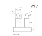
- FIG. 2 is a diagram for explaining parameters representing the shape of the polarizing element 1 of FIG.
- the height means a dimension in a direction perpendicular to the surface of the transparent substrate 11, and the width is orthogonal to the height direction when viewed in a direction along the lattice-shaped convex portion 10 (Y-axis direction). This means the dimension in the direction (X-axis direction).
- the polarizing element 1 When the polarizing element 1 is viewed in the direction along the grid-like convex portions 10 (Y-axis direction), the repetition interval in the X-axis direction of each grid-like convex portion 10 is called a pitch, and the X-axis direction of each grid-like convex portion 10 Is called the grid width.
- the pitch of the polarizing element 1 is smaller than the wavelength of light in the use band.
- the grid-shaped convex portion 10 has a substantially constant width b in the X-axis direction at the grid leg portion 15, and the width in the X-axis direction is smaller than b at a portion close to the tip and above a certain height. .
- the portion where the width is smaller than b is the grid tip 16.
- the height of the grid tip 16 is a.
- the shape of the grid tip part 16 is actually rounded to some extent as shown in FIG. 3, for example. Therefore, the inclination angle ⁇ is defined as the inclination angle of the side surface of the grid front end portion 16 with respect to the transparent substrate 11 at the center position of the height of the grid front end portion 16, that is, the height a / 2.
- Formation of the grid-like convex portions 10 of the polarizing element 1 is performed by forming a reflective layer 12, a dielectric layer 13, and an absorption layer 14 on a transparent substrate 11, and then forming a grid-like mask pattern by, for example, nanoimprinting or photolithography.
- the reflective layer 12, the dielectric layer 13, and the absorption layer 14 on which the mask pattern is not formed are selectively removed by etching to generate a unitary lattice extending in the direction perpendicular to the transparent substrate 11.
- the side surface of the grid tip 16 is inclined by optimizing the etching conditions (gas flow rate, gas pressure, power, substrate cooling temperature).
- the transmittance of the TM wave is increased by making the grid tip 16 in a shape in which the side surface is inclined in a tapering shape.
- the TM wave transmittance is improved because the grid tip 16 is tapered, so that it is difficult to scatter light incident with an angular variation.
- the optical characteristic of the polarizing element 1 is demonstrated using a simulation and a measurement result.
- the transmission axis transmittance characteristic and the absorption axis reflectance characteristic are shown.
- the transmission axis transmittance means the transmittance of polarized light (TM wave) in the transmission axis direction (X-axis direction) incident on the polarizing element 1
- the absorption axis reflectance means the absorption axis direction (Y It means the reflectance of polarized light (TE wave) in the axial direction.
- FIG. 5 shows the absorption axis reflectance of the polarizing element 1 with respect to the inclination angle of the grid tip 16 calculated by simulation when the ratio of the height a to the width b of the grid tip 16 is 6: 9. It is a graph which shows a characteristic.
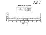
- the absorption axis reflectance increases, it means that the polarized light (TE wave) in the absorption axis direction reflected by the polarizing element 1 becomes stronger. Since such reflected light lowers the extinction ratio, it is preferable that the absorption axis reflectance is low. In many liquid crystal projector applications, the absorption axis reflectance is required to be less than 10%. According to FIG.
- the absorption axis reflectivity increases because the dielectric layer 13 and the dielectric layer 13 when viewed in the direction (Y direction) of FIGS. It is considered that the absorption effect of the reflected light (TE wave) due to these decreases because the size of the absorption layer 14 in the direction along the transparent substrate 11 decreases.
- FIGS. 6 and 7 show the case where the ratio of the height a to the width b of the grid tip 16 is 8:11
- FIGS. 8 and 9 show the case of the grid tip 16.
- 10 and 11 show the case where the ratio of the height a and the width b is 8: 9.
- FIGS. 10 and 11 show the case where the ratio of the height a and the width b of the grid tip 16 is 10: 9.
- 13 shows the transmission axis transmittance characteristics of the polarizing element 1 and the absorption axis reflection with respect to the inclination angle of the grid tip 16 when the ratio of the height a to the width b of the grid tip 16 is 8: 7. The rate characteristic is shown.
- the ratio of the height a to the width b of the grid front end portion 16 is 8: 7, as shown in FIG. % Is over. Therefore, the device characteristic tilt angle in this case is 77 ° ⁇ ⁇ ⁇ 90 °.
- the transmission axis transmittance characteristics are improved by tilting the side surface of the grid tip 16 as shown in FIG.
- the inclination angle ⁇ can be set to 60 ° ⁇ ⁇ ⁇ 90 °.
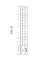
- FIG. 14 is a table showing the range of the inclination angle ⁇ of the grid tip 16 with respect to the ratio of the height a and the width b of the grid tip 16 based on the simulation results of FIGS.
- the transmission axis transmittance of light in each wavelength band was high within the range of the inclination angle ⁇ .
- the device characteristic inclination angle is an inclination angle in a range where the absorption axis reflectance does not exceed 10%.
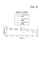
- FIG. 15 shows measured values of transmission axis transmittance characteristics of the polarizing element 1 with respect to the inclination angle ⁇ of the side surface of the grid tip 16 when the ratio of the height a to the width b of the grid tip 16 is 8: 9. It is a graph which compares and shows the result of simulation.
- the outline points are the same as the simulation results shown in FIG.
- the average value of the inclination angle ⁇ is 77 ° and 74 °
- the actual measurement values are indicated by black dots.
- the average value of the inclination angle ⁇ is 74 °
- the average value of the inclination angle ⁇ is because there is variation in the inclination angle of the side surface of the grid tip 16 of the actually produced polarizing element 1.
- the transmission axis transmittance is higher in all bands when the average value of the inclination angle ⁇ is 74 ° than when the average value of the inclination angle ⁇ is 77 °. It has become. Particularly in the blue band, the transmission axis transmittance is greatly improved. Thus, it was shown that the transmission axis transmittance is improved by further tilting the side surface of the grid tip 16 (decreasing the tilt angle ⁇ ).
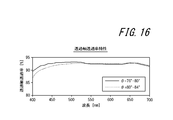
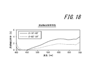
- FIGS. 16 to 19 show measured values of the transmission axis transmittance characteristic, the absorption axis transmittance characteristic, the transmission axis reflectance characteristic, and the absorption axis reflectance characteristic for the two actually produced polarizing elements 1, respectively.
- the absorption axis transmittance means the transmittance of polarized light (TE wave) in the absorption axis direction (Y-axis direction) incident on the polarizing element 1, and the transmission axis reflectance is incident on the polarizing element 1. It means the reflectance of polarized light (TM wave) in the transmission axis direction (X-axis direction).
- the polarization element indicated by the solid line varies in the inclination angle ⁇ of the side surface of the grid tip 16 from 80 ° to 84 °
- the polarization element indicated by the wavy line indicates the inclination of the side surface of the grid tip 16.
- the angle ⁇ varies in the range of 76 ° to 80 °. (Note that the ratio between the height (a) and the width (b) of the grids of the two polarizing elements is close to 2/3 and 8/11.)
- the transmission axis transmittance is substantially constant at about 92% to 93% regardless of the wavelength in the visible light region including the blue band having a wavelength of 430 nm or more.
- a sufficient improvement in transmittance is obtained. Therefore, when the inclination angle ⁇ is 80 ° or less, it is considered that the effect of improving the transmittance according to the present invention is large.
- the absorption axis transmittance indicating the transmittance of the TE wave shown in FIG. 17 is hardly affected even when the inclination angle ⁇ changes.
- the transmission axis reflectivity indicating the reflectivity of the TM wave is substantially 0 at a wavelength of 450 nm, and increases as the distance from the wavelength increases.
- the transmission axis reflectance is smaller than the absorption axis reflectance indicating the reflectance of the TE wave shown in FIG.
- the transmittance of polarized light in the transmission axis direction is controlled by controlling the inclination angle of the side surface of the grid tip portion 16 of the grid-like convex portion 10 having the wire grid structure.
- the effect of improving the transmittance is large for light on the short wavelength side including the blue band in the visible light region.
- the basic structure is the same as the prior art as shown in the cited document 2. For this reason, the reliability can be maintained without changing the manufacturing difficulty level with the conventional polarizing element.
- the polarizing element of the present invention is a polarizing element that designs the wavelength in the green band.
- the predetermined wavelength is not limited to the wavelength in the green band (520 nm to 590 nm), and can be selected from wavelengths in an arbitrary visible light region.
- the absorption axis reflectivity for the design wavelength can be lowered by adjusting the film thickness and refractive index of the dielectric layer, so that the absorption axis reflectivity is 10%.
- the following device characteristic tilt angle range can be ensured.
- the boundary between the grid tip and the grid leg is in the reflective layer, and the grid tip includes the reflective layer, the dielectric layer, and the absorption layer. Absent. As long as the grid tip portion has a tapered shape, a configuration including an absorption layer and a dielectric layer without including a reflection layer, or a configuration including only an absorption layer is possible.
- the transmittance of the TM wave transmitted through the polarizing element 1 can be greatly improved by including the reflective layer at the tip of the grid.
- the application of the polarizing element of the present invention is not limited to a liquid crystal projector. As a polarizing element having a high transmittance of polarized light in the transmission axis direction, it can be used for various applications.
- the polarizing element of the present invention has a high extinction ratio, it can be suitably used as a polarizing element used in a liquid crystal projector.
Landscapes
- Physics & Mathematics (AREA)
- General Physics & Mathematics (AREA)
- Optics & Photonics (AREA)
- Polarising Elements (AREA)
- Liquid Crystal (AREA)
Abstract
本発明の偏光素子は、透明基板と、前記透明基板上に使用帯域の光の波長よりも小さいピッチで配列され、所定方向に延在する格子状凸部とを備え、前記格子状凸部は、前記透明基板上に形成された反射層を含み、且つ、前記所定方向から見たとき、先端部が先細の形状となる方向に側面が傾斜したグリッド先端部が形成されている。
Description
本出願は、日本国特許出願2015-093351号(2015年4月30日出願)の優先権を主張するものであり、当該出願の開示全体を、ここに参照のために取り込む。
本発明は、ワイヤグリッド構造をもつ偏光素子に関するものである。
偏光素子は、一方向の偏光を吸収し、これと直交する方向の偏光を透過させる光学素子である。液晶表示装置では、原理上偏光素子が必要となる。特に、透過型液晶プロジェクタのような、光量の大きな光源を使用する液晶表示装置では、偏光素子は強い輻射線を受けるため、優れた耐熱性が必要となるとともに、数cm程度の大きさと、高い消光比が要求される。これらの要求に応えるための、ワイヤグリッド型の無機偏光素子が提案されている(例えば、特許文献1及び2参照)。
ワイヤグリッド型の偏光素子は、一方向に延在する導体のワイヤ(反射層)を基板上に、使用する波長の帯域よりも狭いピッチ(数十nm~数百nm)で多数並べて配置した構造を有する。この偏光素子に光が入射すると、ワイヤの延在方向に平行な偏光(TE波(S波))は透過することができず、ワイヤの延在方向に垂直な偏光(TM波(P波))は、そのまま透過する。ワイヤグリッド型の偏光素子は、耐熱性に優れ、比較的大きな素子が作製でき、高い消光比を有するので、液晶プロジェクタ等の用途に適している。
例えば、特許文献1に記載のワイヤグリッド型偏光素子では、透明基板上に凸状のラインを一定間隔で配置したグリッド構造層を形成する。このグリッド構造層は樹脂により形成される。次に、スパッタエッチングによりそれぞれの凸状のラインの先端部を山形の形状に加工する。その後、斜めから金属粒子を入射させて、樹脂製のグリッド構造層の先端部の周りに金属層を形成する。
また、特許文献2に記載のワイヤグリッド型偏光素子では、透明基板上に金属ワイヤを形成し、その上に誘電体層と吸収層とを設けている。ワイヤの延在方向に平行な偏光(TE波(S波))は、これら誘電体層と吸収層とによって選択的に吸収される。これにより、液晶プロジェクタに使用された場合、偏光素子の表面で反射された戻り光が、液晶プロジェクタの装置内で再度反射されて生じるゴースト等による、画質の劣化を低減させることができる。
偏光素子において、TM波(P波)の透過率は、高いほど望ましい。しかしながら、従来のワイヤグリッド型の偏光素子では、使用する波長帯域に応じた、ピッチとグリッド幅との関係から、原理的に設計波長から短波長側になればなるほど、光の透過率が低下する。液晶プロジェクタで使用される可視光領域(赤色帯域:波長λ=600~680nm、緑色帯域:波長λ=520nm~590nm、青色帯域:λ=430nm~510nm)では、緑色帯域の波長を設計波長とする偏光素子の場合、青色帯域がもっとも透過率が低くなる。偏光素子のグリッド幅を細くする事で、透過率を上げることができることが知られているが、実際にグリッド幅を狭めたパターンを形成することは、難易度が高く信頼性を維持することも困難である。
本発明は、従来における前記諸問題を解決し、以下の目的を達成することを課題とする。即ち、本発明は、透過軸方向の光透過特性を改善したワイヤグリッド型の偏光素子を提供することを目的とする。
本発明は、本発明者による知見に基づくものであり、前記課題を解決するための手段としては以下の通りである。即ち、
<1>ワイヤグリッド構造を持つ偏光素子であって、透明基板と、前記透明基板上に使用帯域の光の波長よりも小さいピッチで配列され、所定方向に延在する格子状凸部とを備え、前記格子状凸部は、前記透明基板上に形成された反射層を含み、且つ、前記所定方向から見たとき、先端部が先細の形状となる方向に側面が傾斜したグリッド先端部が形成されている偏光素子である。
<2>前記グリッド先端部の側面の前記透明基板に対する傾斜角をθとし、前記所定方向から見たときの前記グリッド先端部の高さをa、前記格子状凸部の幅をb、
θ0=arctan(2a/b)とするとき、
2/3≦a/b≦8/7
及び、
θ0≦θ<90°(θ0=arctan(2a/b))
を満足する前記<1>に記載の偏光素子である。
<3>前記傾斜角θは、前記所定方向から見たとき、前記グリッド先端部の高さ方向の中心位置における前記グリッド先端部の前記側面の接線の傾斜角として規定される前記<2>に記載の偏光素子である。
<4>前記傾斜角θは、θ≦80°である前記<2>又は<3>に記載の偏光素子である。
<5>前記偏光素子は、可視光領域の所定の波長の光に対して設計され、前記傾斜角θは、前記所定の波長の光の吸収軸方向の反射率を10%以下とする角度範囲から選択される前記<2>から<4>の何れかに記載の偏光素子である。
<6>前記グリッド先端部は、前記透明基板側から順に、反射層、誘電体層及び吸収層により構成されている前記<1>から<5>の何れかに記載の偏光素子である。
<1>ワイヤグリッド構造を持つ偏光素子であって、透明基板と、前記透明基板上に使用帯域の光の波長よりも小さいピッチで配列され、所定方向に延在する格子状凸部とを備え、前記格子状凸部は、前記透明基板上に形成された反射層を含み、且つ、前記所定方向から見たとき、先端部が先細の形状となる方向に側面が傾斜したグリッド先端部が形成されている偏光素子である。
<2>前記グリッド先端部の側面の前記透明基板に対する傾斜角をθとし、前記所定方向から見たときの前記グリッド先端部の高さをa、前記格子状凸部の幅をb、
θ0=arctan(2a/b)とするとき、
2/3≦a/b≦8/7
及び、
θ0≦θ<90°(θ0=arctan(2a/b))
を満足する前記<1>に記載の偏光素子である。
<3>前記傾斜角θは、前記所定方向から見たとき、前記グリッド先端部の高さ方向の中心位置における前記グリッド先端部の前記側面の接線の傾斜角として規定される前記<2>に記載の偏光素子である。
<4>前記傾斜角θは、θ≦80°である前記<2>又は<3>に記載の偏光素子である。
<5>前記偏光素子は、可視光領域の所定の波長の光に対して設計され、前記傾斜角θは、前記所定の波長の光の吸収軸方向の反射率を10%以下とする角度範囲から選択される前記<2>から<4>の何れかに記載の偏光素子である。
<6>前記グリッド先端部は、前記透明基板側から順に、反射層、誘電体層及び吸収層により構成されている前記<1>から<5>の何れかに記載の偏光素子である。
本発明によれば、従来における前記諸問題を解決し、前記目的を達成することができ、透過軸方向の偏光の光透過特性を改善したワイヤグリッド型の偏光素子を提供することができる。
以下、本発明の実施の形態について、図面を参照して説明する。
<偏光素子の構成>
図1は、本発明の一実施の形態に係る偏光素子1を示す概略断面図である。図1に示すように、偏光素子1は、使用帯域の光に透明な透明基板11と、透明基板11の一方の面上に使用帯域の光の波長よりも小さいピッチで配列された格子状凸部10を構成する反射層12と、反射層12上に形成された誘電体層13と、誘電体層13上に形成された吸収層14とを備える。すなわち、偏光素子1は、透明基板11側から反射層12と誘電体層13と吸収層14とがこの順に積層された格子状凸10部が、透明基板11上に一定間隔に並んだ一次元格子状のワイヤグリッド構造を有する。
図1は、本発明の一実施の形態に係る偏光素子1を示す概略断面図である。図1に示すように、偏光素子1は、使用帯域の光に透明な透明基板11と、透明基板11の一方の面上に使用帯域の光の波長よりも小さいピッチで配列された格子状凸部10を構成する反射層12と、反射層12上に形成された誘電体層13と、誘電体層13上に形成された吸収層14とを備える。すなわち、偏光素子1は、透明基板11側から反射層12と誘電体層13と吸収層14とがこの順に積層された格子状凸10部が、透明基板11上に一定間隔に並んだ一次元格子状のワイヤグリッド構造を有する。
それぞれの格子状凸部10は、格子状凸部10のそれぞれの一次元格子の凸部が延在する方向(所定方向)から見たとき、透明基板11から垂直方向に側面が平行に延びるグリッド脚部15と、グリッド脚部15上に位置し、先端に向けて先細の形状となる方向に側面が傾斜したグリッド先端部16とに分かれている。そして、グリッド脚部15とグリッド先端部16との境界は、反射層12に位置する。すなわち、グリッド脚部15は、反射層12の一部により構成され、グリッド先端部16は反射層12の一部、誘電体層13及び吸収層14により構成される。なお、以下の説明において、格子状凸部10の一次元格子の凸部が延在する方向をY軸方向と呼び、透明基板11に沿いY軸方向に直交する方向をX軸方向と呼ぶ。この場合、偏光素子1に入射する光は、透明基板11の格子状凸部10が形成された側に、好適にはX軸方向及びY軸方向に直交する方向から入射する。
吸収層14は金属、半導体など光学定数の消衰定数が零でない、すなわち光吸収作用を持つ物質である。なお、偏光素子1は、誘電体層13と吸収層14との間に、吸収層14の拡散防止を目的としてTa,W,Nb,Tiなどの金属膜を拡散バリア層として備えても良い。また、偏光素子1は、必要に応じて、光学特性の変化が応用上影響を与えない範囲で、最上部に耐湿性などの信頼性改善の目的でSiO2などの保護膜を堆積してもよい。
そして、偏光素子1は、透過、反射、干渉、光学異方性による偏光波の選択的光吸収の4つの作用を利用することで、Y軸方向に平行な電界成分をもつ偏光波(TE波(S波))を減衰させ、X軸方向に平行な電界成分をもつ偏光波(TM波(P波))を透過させる。したがって、Y軸方向は偏光素子1の吸収軸の方向であり、X軸方向は偏光素子1の透過軸の方向である。
吸収層14及び誘電体層13を透過したTM波は、高い透過率で反射層12を透過する。一方、TE波は、吸収層14の光吸収作用によって減衰される。一次元格子状の反射層12は、ワイヤグリッドとして機能し、吸収層14及び誘電体層13を透過したTE波を反射する。また、誘電体層13の厚さ及び屈折率を適宜調整することによって、反射層12で反射したTE波は、吸収層14を通過する際に一部は吸収され、一部は反射し、反射層12に戻る。また吸収層14を通過した光は干渉して減衰する。以上のようにして、偏光素子1は、TE波の選択的減衰を行うことにより、所望の偏光特性を得ることができる。
[透明基板]
透明基板11は、使用帯域の光に対して透明で、屈折率が1.1~2.2の材料、例えば、ガラス、サファイア、水晶などで構成されている。本実施の形態では、透明基板11の構成材料として、熱伝導性の高い水晶やサファイア基板を用いることが好ましい。これにより、強い光に対して高い耐光性を有することとなり、発熱量の多いプロジェクタの光学エンジン用の偏光素子として有用となる。
透明基板11は、使用帯域の光に対して透明で、屈折率が1.1~2.2の材料、例えば、ガラス、サファイア、水晶などで構成されている。本実施の形態では、透明基板11の構成材料として、熱伝導性の高い水晶やサファイア基板を用いることが好ましい。これにより、強い光に対して高い耐光性を有することとなり、発熱量の多いプロジェクタの光学エンジン用の偏光素子として有用となる。
また、透明基板11が水晶のような光学活性の結晶からなる場合、結晶の光学軸に対して平行方向又は垂直方向に格子状凸部10を配置することにより、優れた光学特性を得ることができる。ここで、光学軸とは、その方向に進む光のO(常光線)とE(異常光線)の屈折率の差が最小となる方向軸である。
なお、偏光素子1の用途によっては、ガラス、特に、石英(屈折率1.46)やソーダ石灰ガラス(屈折率1.51)を用いてもよい。ガラス材料の成分組成は特に制限されず、例えば光学ガラスとして広く流通しているケイ酸塩ガラスなどの安価なガラス材料を用いることができ、製造コストの低減を図ることができる。
[反射層]
反射層12は、透明基板11上に吸収軸であるY軸方向に帯状に延びた金属薄膜が配列されてなるものである。すなわち、反射層12は、ワイヤグリッド型偏光子としての機能を有し、透明基板11のワイヤグリッドが形成された面に向かって入射した光のうち、ワイヤグリッドの凸部が延在する方向に平行な方向(Y軸方向)に電界成分をもつ偏光波(TE波(S波))を減衰させ、ワイヤグリッドの凸部が延在する方向と直交する方向(X軸方向)に電界成分をもつ偏光波(TM波(P波))を透過させる。
反射層12は、透明基板11上に吸収軸であるY軸方向に帯状に延びた金属薄膜が配列されてなるものである。すなわち、反射層12は、ワイヤグリッド型偏光子としての機能を有し、透明基板11のワイヤグリッドが形成された面に向かって入射した光のうち、ワイヤグリッドの凸部が延在する方向に平行な方向(Y軸方向)に電界成分をもつ偏光波(TE波(S波))を減衰させ、ワイヤグリッドの凸部が延在する方向と直交する方向(X軸方向)に電界成分をもつ偏光波(TM波(P波))を透過させる。
反射層12の構成材料には、使用帯域の光に対して反射性を有する材料であれば特に制限されず、例えばAl、Ag、Cu、Mo、Cr、Ti、Ni、W、Fe、Si、Ge、Teなどの金属単体若しくはこれらを含む合金あるいは半導体材料を用いることができる。なお、金属材料以外にも、例えば着色等により表面の反射率が高く形成された金属以外の無機膜や樹脂膜で構成されていてもよい。
[誘電体層]
誘電体層13は、吸収層14で反射した偏光に対して、吸収層14を透過し、反射層12で反射した当該偏光の位相が半波長ずれる膜厚で形成されている。具体的な膜厚は、偏光の位相を調整し、干渉効果を高めることが可能な1~500nmの範囲で適宜設定される。
誘電体層13は、吸収層14で反射した偏光に対して、吸収層14を透過し、反射層12で反射した当該偏光の位相が半波長ずれる膜厚で形成されている。具体的な膜厚は、偏光の位相を調整し、干渉効果を高めることが可能な1~500nmの範囲で適宜設定される。
誘電体層13を構成する材料は、SiO2、Al2O3、酸化ベリリウム、酸化ビスマス、等の金属酸化物、MgF2、氷晶石、ゲルマニウム、二酸化チタン、ケイ素、フッ化マグネシウム、窒化ボロン、酸化ボロン、酸化タンタル、炭素並びにそれらの組み合わせなどの一般的な材料を用いることができる。また、誘電体層13の屈折率は、1.0より大きく2.5以下とすることが好ましい。なお、反射層12の光学特性は、周囲の屈折率によっても影響を受けるため、誘電体層13の材料により偏光素子特性を制御してもよい。
[吸収層]
吸収層14は、金属、半導体など光学定数の消衰定数が零でない、光吸収作用を持つ物質の1種以上から構成され、その材料は、適用される光の波長範囲によって選択される。金属材料としては、Ta、Al、Ag、Cu、Au、Mo、Cr、Ti、W、Ni、Fe、Sn単体若しくはこれらを含む合金が挙げられる。半導体材料としては、Si、Ge、Te、ZnO、シリサイド材料(β-FeSi2、MgSi2、NiSi2、BaSi2、CrSi2、CoSi2、TaSi等)などが挙げられる。これにより、偏光素子1は、適用される可視光域に対して高い消光比を備えることができる。
吸収層14は、金属、半導体など光学定数の消衰定数が零でない、光吸収作用を持つ物質の1種以上から構成され、その材料は、適用される光の波長範囲によって選択される。金属材料としては、Ta、Al、Ag、Cu、Au、Mo、Cr、Ti、W、Ni、Fe、Sn単体若しくはこれらを含む合金が挙げられる。半導体材料としては、Si、Ge、Te、ZnO、シリサイド材料(β-FeSi2、MgSi2、NiSi2、BaSi2、CrSi2、CoSi2、TaSi等)などが挙げられる。これにより、偏光素子1は、適用される可視光域に対して高い消光比を備えることができる。
なお、半導体材料を用いる場合、吸収作用に半導体のバンドギャップエネルギーが関与するため、バンドギャップエネルギーが使用帯域以下であることが必要である。例えば、可視光で使用する場合、波長400nm以上での吸収、すなわちバンドギャップとしては3.1eV以下の材料を使用する必要がある。
なお、吸収層14は、蒸着法やスパッタ法により、膜が高い密度で形成することができる。また、吸収層14は、材料の異なる2層以上から構成されていてもよい。
このような構成の偏光素子1によれば、透過、反射、干渉、偏光波の選択的光吸収の4つの作用を利用することで、反射層12の格子に平行なY軸方向の電界成分をもつ偏光波(TE波(S波))を減衰させ、格子に垂直なX軸方向の電界成分をもつ偏光波(TM波(P波))を透過させることができる。すなわち、TE波は、吸収層14の偏光波の選択的光吸収作用によって減衰され、吸収層14及び誘電体層13を透過したTE波は、ワイヤグリッドとして機能する格子状の反射層12によって反射される。ここで、誘電体層13の厚さ、屈折率を適宜調整することによって、反射層12で反射したTE波について、吸収層14を透過する際に一部を反射し、反射層12に戻すことができ、また、吸収層14を通過した光を干渉により減衰させることができる。以上のようにしてTE波の選択的減衰を行うことにより、所望の偏光特性を得ることができる。
[グリッド先端部]
次に、グリッド先端部16の形状について説明する。
次に、グリッド先端部16の形状について説明する。
図2は、図1の偏光素子1の形状を表すパラメータを説明する図である。以下において、高さとは、透明基板11の面に垂直な方向の寸法を意味し、幅とは、格子状凸部10に沿う方向(Y軸方向)に見たときの高さ方向に直交する方向(X軸方向)の寸法を意味する。
偏光素子1を格子状凸部10に沿う方向(Y軸方向)に見たとき、各格子状凸部10のX軸方向の繰り返し間隔をピッチと呼び、各格子状凸部10のX軸方向の幅をグリッド幅と呼ぶ。偏光素子1のピッチは、使用帯域の光の波長よりも小さい。また、格子状凸部10はグリッド脚部15では、X軸方向に略一定の幅bを有し、先端部に近い、ある高さ以上の部分でX軸方向の幅がbよりも小さくなる。この幅がbより小さくなった部分がグリッド先端部16である。ここで、グリッド先端部16の高さをaとする。また、グリッド先端部16の側面の透明基板11の面に対する傾斜角をθとする。図2に示すように、グリッド先端部16の側面の傾斜角θが一定の場合には、θ0=arctan(2a/b)とするとき、傾斜角θは、
θ0≦θ<90°
の範囲の角度となる。
θ0≦θ<90°
の範囲の角度となる。
しかし、格子状凸部10は非常に微細な構造であるため、グリッド先端部16の形状は、例えば図3に示すように、実際にはある程度の丸みを帯びる。そこで、傾斜角θは、グリッド先端部16の高さの中心位置、すなわち高さa/2の位置におけるグリッド先端部16の側面の透明基板11に対する傾斜角として規定する。
偏光素子1の格子状凸部10の形成は、透明基板11上に、反射層12、誘電体層13、吸収層14を成膜した後、例えばナノインプリント、フォトリソグラフィ等により格子状のマスクパターンを形成することによる。マスクパターンが形成されていない反射層12、誘電体層13及び吸収層14をエッチングにより選択的に除去して、透明基板11に対して垂直方向に延びる一元格子を生成する。このとき、エッチング条件(ガス流量、ガス圧、パワー、基板の冷却温度)を最適化することによって、グリッド先端部16の側面に傾斜を持たせている。
<光学特性の評価>
このように、Y軸方向から見たとき、グリッド先端部16を先細の形状になる方向に側面を傾斜させた形状にすることによって、TM波の透過率が高くなる。このように、TM波透過率が向上するのは、グリッド先端部16を先細にすることで、角度バラツキを持って入射してくる光に対して散乱し難くなるためと考えられる。以下に、シミュレーション及び実測結果を用いて、偏光素子1の光学特性について説明する。
このように、Y軸方向から見たとき、グリッド先端部16を先細の形状になる方向に側面を傾斜させた形状にすることによって、TM波の透過率が高くなる。このように、TM波透過率が向上するのは、グリッド先端部16を先細にすることで、角度バラツキを持って入射してくる光に対して散乱し難くなるためと考えられる。以下に、シミュレーション及び実測結果を用いて、偏光素子1の光学特性について説明する。
[シミュレーション]
図4~図13に、それぞれグリッド先端部16の高さ(a)と幅(b)との比を種々に変えて、シミュレーションにより計算された、グリッド先端部16の傾斜角に対する偏光素子1の透過軸透過率特性、及び、吸収軸反射率特性を示す。透過軸透過率とは、偏光素子1に入射する透過軸方向(X軸方向)の偏光(TM波)の透過率を意味し、吸収軸反射率とは、偏光素子1の吸収軸方向(Y軸方向)の偏光(TE波)の反射率を意味する。これらのグラフは、何れも緑色帯域(波長520nm~590nm(所定の波長))の光に対して最適化されるように設計された偏光素子1に対するものである。
図4~図13に、それぞれグリッド先端部16の高さ(a)と幅(b)との比を種々に変えて、シミュレーションにより計算された、グリッド先端部16の傾斜角に対する偏光素子1の透過軸透過率特性、及び、吸収軸反射率特性を示す。透過軸透過率とは、偏光素子1に入射する透過軸方向(X軸方向)の偏光(TM波)の透過率を意味し、吸収軸反射率とは、偏光素子1の吸収軸方向(Y軸方向)の偏光(TE波)の反射率を意味する。これらのグラフは、何れも緑色帯域(波長520nm~590nm(所定の波長))の光に対して最適化されるように設計された偏光素子1に対するものである。
図4は、グリッド先端部16の高さaと幅bとの比が6:9の場合について、シミュレーションにより計算された、グリッド先端部16の傾斜角に対する偏光素子1の透過軸透過率特性を示すグラフである。透過軸透過率が高ければ、高い強度の所望の光が偏光素子1を透過する。図4に示すように、傾斜角θが、90°から傾くにつれて(すなわち、グラフ上で右端から左にずれるにつれて)、青色帯域(波長λ=430~510nm)、緑色帯域(波長λ=520~590nm)及び赤色帯域(波長λ=600~680nm)の何れの帯域においても、透過率が高くなる。特に、青色帯域については、透過率の上昇幅が大きいことがわかる。
一方、図5は、グリッド先端部16の高さaと幅bとの比が6:9の場合について、シミュレーションにより計算された、グリッド先端部16の傾斜角に対する偏光素子1の吸収軸反射率特性を示すグラフである。吸収軸反射率が高くなると、偏光素子1により反射される吸収軸方向の偏光(TE波)が強くなることを意味する。このような反射光は消光比を低下させるため、吸収軸反射率は低い方が好ましい。多くの液晶プロジェクタ用途では、吸収軸反射率は10%未満であることが要求される。図5によれば、傾斜角θが小さいほど、このシミュレーションにおける偏光素子1の設計波長である緑色帯域の吸収軸反射率が高くなり、傾斜角θが61°より小さくなると吸収軸反射率が10%を超える。したがって、液晶プロジェクタ用途で許容される傾斜角θの値は、61°≦θ<90°となる。この角度のことを、デバイス特性傾斜角と呼ぶ。なお、グリッド先端部16の傾きを大きくすると(傾斜角θを小さくすると)、吸収軸反射率が高くなるのは、図1、2の方向(Y方向)に見たときの誘電体層13及び吸収層14の透明基板11に沿う方向の大きさが小さくなるためにこれらによる反射光(TE波)の吸収効果が低下するためと考えられる。
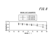
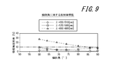
図4及び図5と同様に、図6及び図7は、グリッド先端部16の高さaと幅bとの比が8:11の場合について、図8及び図9は、グリッド先端部16の高さaと幅bとの比が8:9の場合について、図10及び図11は、グリッド先端部16の高さaと幅bとの比が10:9の場合について、図12及び図13は、グリッド先端部16の高さaと幅bとの比が8:7の場合について、それぞれ、グリッド先端部16の傾斜角に対する偏光素子1の透過軸透過率特性、及び、吸収軸反射率特性を示している。グリッド先端部16の高さaと幅bとの比に関わらず、グリッド先端部16の側面の傾斜が大きいほど(傾斜角θが小さいほど)、青色帯域、緑色帯域及び赤色帯域の何れの帯域においても、透過軸透過率の改善がみられる。また、何れの場合も、青色帯域の透過軸透過率の上昇が他の帯域よりも大きい。一方、グリッド先端部16の高さaと幅bとの比が8:7の場合に、図13に示すように、θ<77°になると緑色帯域の波長の光の吸収軸反射率が10%を超えている。したがって、この場合のデバイス特性傾斜角度は、77°≦θ<90°である。また、グリッド先端部16の高さaと幅bとの比が8:9の場合に、図8に示すようにグリッド先端部16の側面を傾けることによる透過軸透過率の特性が向上の効果が高く、傾斜角θは60°≦θ<90°とすることができる。
図14は、図4~図13のシミュレーション結果に基づく、グリッド先端部16の高さaと幅bとの比に対する、グリッド先端部16の傾斜角θの範囲を示す表である。この表において、シミュレーション傾斜角θは、シミュレーションを行った傾斜角の範囲であり、既に説明したように、θ0≦θ<90°(θ0=arctan(2a/b))の範囲である。上記図4~図13の例では、グリッド先端部16の形状を高さaと幅bの比をa/bで示すとき、
2/3≦a/b≦8/7
に含まれる何れの範囲においても、上記傾斜角θの範囲で各波長帯域の光の透過軸透過率が高くなることが確認された。また、上述のように、デバイス特性傾斜角は、吸収軸反射率が10%を超えない範囲の傾斜角である。偏光素子1を液晶プロジェクタ等に使用する場合には、傾斜角θは、このデバイス特性傾斜角の範囲を満たすことが望ましい。
2/3≦a/b≦8/7
に含まれる何れの範囲においても、上記傾斜角θの範囲で各波長帯域の光の透過軸透過率が高くなることが確認された。また、上述のように、デバイス特性傾斜角は、吸収軸反射率が10%を超えない範囲の傾斜角である。偏光素子1を液晶プロジェクタ等に使用する場合には、傾斜角θは、このデバイス特性傾斜角の範囲を満たすことが望ましい。
[実測結果とシミュレーションとの対比]
次に、実際にワイヤグリッド構造の偏光素子1を作製して、得られた透過軸透過率特性を、シミュレーション結果と比較した結果について説明する。図15は、グリッド先端部16の高さaと幅bとの比が8:9の場合について、グリッド先端部16の側面の傾斜角θに対する偏光素子1の透過軸透過率特性の実測値とシミュレーションの結果とを対比して示すグラフである。
次に、実際にワイヤグリッド構造の偏光素子1を作製して、得られた透過軸透過率特性を、シミュレーション結果と比較した結果について説明する。図15は、グリッド先端部16の高さaと幅bとの比が8:9の場合について、グリッド先端部16の側面の傾斜角θに対する偏光素子1の透過軸透過率特性の実測値とシミュレーションの結果とを対比して示すグラフである。
図15において、白抜きの点は、図8に示されたシミュレーション結果と同じものである。これに対して、傾斜角θの平均値が77°と74°の場合について、実測値を黒塗りの点で示している。ここで、傾斜角θの平均値が74°の場合は、青色帯域(波長λ=430~510nm)の実測値と緑色帯域(波長λ=520~590nm)の実測値とが92.6%付近で重なった点となっている。なお、傾斜角θの平均値としたのは、実際に作製した偏光素子1のグリッド先端部16の側面の傾斜角度にはバラツキがあるためである。
図15からわかるように、実測結果においても傾斜角θの平均値が77°の時よりも、傾斜角θの平均値が74°の場合の方が、全ての帯域で透過軸透過率が高くなっている。特に青色帯域においては、透過軸透過率が大幅に向上している。このように、グリッド先端部16の側面をより傾けることにより(傾斜角θを小さくすることにより)、透過軸透過率が向上することが示された。
次に、図16~図19は、実際に作製した2つの偏光素子1について、それぞれ、透過軸透過率特性、吸収軸透過率特性、透過軸反射率特性及び吸収軸反射率特性の実測値を示す図である。ここで、吸収軸透過率とは、偏光素子1に入射する吸収軸方向(Y軸方向)の偏光(TE波)の透過率を意味し、透過軸反射率とは、偏光素子1に入射する透過軸方向(X軸方向)の偏光(TM波)の反射率を意味する。それぞれのグラフで、実線で示される偏光素子は、グリッド先端部16の側面の傾斜角θが80°~84°でバラついており、波線で示される偏光素子は、グリッド先端部16の側面の傾斜角θが76°~80°の範囲でバラついている。(なお、2つの偏光素子のグリッドの高さ(a)と幅(b)との比は、2/3と8/11で近い値としている。)
図16に示す、偏光素子1のTM波の透過率を示す透過軸透過率は、グリッド先端部16の側面の傾斜角θを小さくしたときに、特に青色帯域(波長λ=430~510nm)において大幅な向上がみられる。また、傾斜角θの値が、76°~80°の場合は、波長が430nm以上の青色帯域を含む可視光領域で、透過軸透過率が波長によらず約92%~93%で略一定となっており、十分な透過率の向上が得られている。したがって、傾斜角θが80°以下の場合は、本発明による透過率の向上効果が大きいと考えられる。なお、図4、図8、図10に示されるシミュレーションの例では、傾斜角θが80°以下であれば、青色帯域、緑色帯域および赤色帯域の透過軸透過率の間の差が、0.5%~1%程度の範囲の小さな値となっている。このため、偏光素子1を透過した光の波長帯域毎に均等に透過するので、色彩の変化が少ない。
これに対して、図17に示されるTE波の透過率を示す吸収軸透過率は、傾斜角θが変化してもほとんど影響を受けない。また、図18に示されるように、TM波の反射率を示す透過軸反射率は、波長450nmでほぼ0であり、この波長から離れるほど大きくなっている。しかし、透過軸反射率は、図19に示されるTE波の反射率を示す吸収軸反射率よりも小さくなっている。
以上説明したように本発明に係る偏光素子1によれば、ワイヤグリッド構造の格子状凸部10のグリッド先端部16の側面の傾斜角度を制御することによって、透過軸方向の偏光の透過率を向上させることができる。特に、可視光領域のうち青色帯域を含む短波長側の光に対して、透過率向上の効果が大きい。また、本発明では、格子状凸部10全体ではなくグリッド先端部16のみの形状を変えたので、基本的な構造は引用文献2に示されるような従来技術と同一である。このため、従来の偏光素子と製造上の難易度が変わることなく、信頼性も維持することができる。
なお、本発明は、上記実施形態のみに限定されるものではなく、本発明の要旨を逸脱しない範囲内において種々の変更が可能であることは勿論である。また、図面は模式的なものであり、各寸法の比率等は現実のものとは異なることがある。具体的な寸法等は上記説明を参酌して判断すべきものである。また、図面相互間においても互いの寸法の関係や比率が異なる部分が含まれていることは勿論である。
上記実施の形態では、実施例として、緑色帯域を設計波長として設計された偏光素子について、シミュレーションおよび実測の結果を示したが、本発明の偏光素子は緑色帯域の波長を設計波長する偏光素子に限られない。すなわち、所定の波長は、緑色帯域の波長(520nm~590nm)に限られず、任意の可視光領域の波長から選択することができる。グリッド先端部を先細の形状とすることによって、何れの波長を設計波長とした場合も、上述のように透過軸透過率の向上が期待できる。特に、設計波長の短波長側での効果が大きいものと期待できる。また、緑色帯域以外の波長を設計波長とする場合も、誘電体層の膜厚および屈折率等を調整して、当該設計波長に対する吸収軸反射率を低くできるので、吸収軸反射率が10%以下となるデバイス特性傾斜角の範囲を確保することができる。さらに、上記実施の形態において、グリッド先端部とグリッド脚部との境界は反射層にあり、グリッド先端部には反射層、誘電体層及び吸収層を含むものとしたが、これには限られない。グリッド先端部は、先細の形状となっていれば、反射層を含まず吸収層と誘電体層とで構成される構成、又は、吸収層のみで構成される構成も可能である。ただし、グリッド先端部に反射層を含むことによって、偏光素子1を透過するTM波の透過率をより大きく向上させることができる。また、本発明の偏光素子の用途は、液晶プロジェクタに限られない。透過軸方向の偏光の透過率が高い偏光素子として、種々の用途に利用することが可能である。
本願発明の偏光素子は、高い消光比を有するので、液晶プロジェクタに使用される偏光素子として好適に利用可能である。
1 偏光素子
10 格子状凸部
11 透明基板
12 反射層
13 誘電体層
14 吸収層
15 グリッド脚部
16 グリッド先端部
10 格子状凸部
11 透明基板
12 反射層
13 誘電体層
14 吸収層
15 グリッド脚部
16 グリッド先端部
Claims (6)
- ワイヤグリッド構造を持つ偏光素子であって、
透明基板と、
前記透明基板上に使用帯域の光の波長よりも小さいピッチで配列され、所定方向に延在する格子状凸部と
を備え、
前記格子状凸部は、前記透明基板上に形成された反射層を含み、且つ、前記所定方向から見たとき、先端部が先細の形状となる方向に側面が傾斜したグリッド先端部が形成されている偏光素子。 - 前記グリッド先端部の側面の前記透明基板に対する傾斜角をθとし、前記所定方向から見たときの前記グリッド先端部の高さをa、前記格子状凸部の幅をb、
θ0=arctan(2a/b)とするとき、
2/3≦a/b≦8/7
及び、
θ0≦θ<90°
を満足する請求項1に記載の偏光素子。 - 前記傾斜角θは、前記所定方向から見たとき、前記グリッド先端部の高さ方向の中心位置における前記グリッド先端部の前記側面の接線の傾斜角として規定される請求項2に記載の偏光素子。
- 前記傾斜角θは、θ≦80°である請求項2に記載の偏光素子。
- 前記偏光素子は、可視光領域の所定の波長の光に対して設計され、前記傾斜角θは、前記所定の波長の光の吸収軸方向の反射率を10%以下とする角度範囲から選択される請求項2に記載の偏光素子。
- 前記グリッド先端部は、前記透明基板側から順に、反射層、誘電体層及び吸収層により構成されている請求項1に記載の偏光素子。
Priority Applications (2)
| Application Number | Priority Date | Filing Date | Title |
|---|---|---|---|
| CN201680022107.3A CN107407770B (zh) | 2015-04-30 | 2016-04-14 | 偏振元件 |
| US15/564,503 US10698147B2 (en) | 2015-04-30 | 2016-04-14 | Polarizing element |
Applications Claiming Priority (2)
| Application Number | Priority Date | Filing Date | Title |
|---|---|---|---|
| JP2015093351A JP5960319B1 (ja) | 2015-04-30 | 2015-04-30 | 偏光素子 |
| JP2015-093351 | 2015-04-30 |
Publications (1)
| Publication Number | Publication Date |
|---|---|
| WO2016174838A1 true WO2016174838A1 (ja) | 2016-11-03 |
Family
ID=56550521
Family Applications (1)
| Application Number | Title | Priority Date | Filing Date |
|---|---|---|---|
| PCT/JP2016/002023 Ceased WO2016174838A1 (ja) | 2015-04-30 | 2016-04-14 | 偏光素子 |
Country Status (4)
| Country | Link |
|---|---|
| US (1) | US10698147B2 (ja) |
| JP (1) | JP5960319B1 (ja) |
| CN (1) | CN107407770B (ja) |
| WO (1) | WO2016174838A1 (ja) |
Families Citing this family (23)
| Publication number | Priority date | Publication date | Assignee | Title |
|---|---|---|---|---|
| JP6935318B2 (ja) * | 2016-12-28 | 2021-09-15 | デクセリアルズ株式会社 | 偏光板及びその製造方法、並びに光学機器 |
| JP6230689B1 (ja) * | 2016-12-28 | 2017-11-15 | デクセリアルズ株式会社 | 偏光板及びその製造方法、並びに光学機器 |
| JP6302040B1 (ja) * | 2016-12-28 | 2018-03-28 | デクセリアルズ株式会社 | 偏光板及びその製造方法、並びに光学機器 |
| JP6312917B1 (ja) * | 2017-02-07 | 2018-04-18 | デクセリアルズ株式会社 | 無機偏光板及びその製造方法、並びに光学機器 |
| JP6410906B1 (ja) | 2017-09-26 | 2018-10-24 | デクセリアルズ株式会社 | 偏光素子及び光学機器 |
| TWI702424B (zh) * | 2017-10-24 | 2020-08-21 | 日商旭化成股份有限公司 | 影像顯示裝置、線柵偏光板及其製造方法、線柵偏光板之觀測方法、及、線柵偏光板之偏光軸方向之推定方法 |
| CN109975910B (zh) | 2017-12-28 | 2022-02-18 | 迪睿合株式会社 | 偏振光板及其制造方法以及光学设备 |
| JP7101028B2 (ja) * | 2018-04-12 | 2022-07-14 | デクセリアルズ株式会社 | 偏光素子及びその製造方法、並びに光学機器 |
| JP6826073B2 (ja) | 2018-05-31 | 2021-02-03 | デクセリアルズ株式会社 | 偏光板及びその製造方法、並びに光学機器 |
| JP7226936B2 (ja) * | 2018-07-26 | 2023-02-21 | デクセリアルズ株式会社 | 偏光板及び光学機器 |
| JP6577641B2 (ja) * | 2018-08-20 | 2019-09-18 | デクセリアルズ株式会社 | 偏光板及びその製造方法、並びに光学機器 |
| JP7226966B2 (ja) * | 2018-10-26 | 2023-02-21 | デクセリアルズ株式会社 | 偏光板及び偏光板の製造方法 |
| JP7262720B2 (ja) * | 2018-11-02 | 2023-04-24 | エルジー・ケム・リミテッド | 円偏光板 |
| JP7333168B2 (ja) | 2018-11-19 | 2023-08-24 | デクセリアルズ株式会社 | 偏光素子、偏光素子の製造方法及び光学機器 |
| JP7075372B2 (ja) * | 2019-04-26 | 2022-05-25 | デクセリアルズ株式会社 | 偏光板及びその製造方法、並びに光学機器 |
| JP7204611B2 (ja) * | 2019-08-05 | 2023-01-16 | デクセリアルズ株式会社 | 偏光板およびその製造方法 |
| CN114829986B (zh) * | 2019-12-02 | 2025-05-16 | 3M创新有限公司 | 光学超表面膜 |
| JP7219735B2 (ja) * | 2020-03-26 | 2023-02-08 | デクセリアルズ株式会社 | 偏光板及びその製造方法、並びに光学機器 |
| JP2023523765A (ja) * | 2020-05-01 | 2023-06-07 | スリーエム イノベイティブ プロパティズ カンパニー | 反射光学メタ表面フィルム |
| JP7394020B2 (ja) * | 2020-05-25 | 2023-12-07 | デクセリアルズ株式会社 | 偏光板及びその製造方法、ならびに光学機器 |
| CN113867032A (zh) | 2020-06-30 | 2021-12-31 | 京东方科技集团股份有限公司 | 一种线栅偏光片及其制造方法 |
| JP2021058805A (ja) * | 2021-01-21 | 2021-04-15 | 株式会社三洋物産 | 遊技機 |
| JP7592521B2 (ja) * | 2021-03-15 | 2024-12-02 | デクセリアルズ株式会社 | 光学機器 |
Citations (5)
| Publication number | Priority date | Publication date | Assignee | Title |
|---|---|---|---|---|
| JP2007058106A (ja) * | 2005-08-26 | 2007-03-08 | Nippon Zeon Co Ltd | 偏光分離フィルム、偏光分離フィルムの製造方法、および液晶表示装置 |
| JP2010145854A (ja) * | 2008-12-19 | 2010-07-01 | Asahi Kasei E-Materials Corp | ワイヤグリッド偏光子 |
| JP2011133912A (ja) * | 2011-04-01 | 2011-07-07 | Sony Corp | 光学装置の製造方法 |
| JP2013167824A (ja) * | 2012-02-16 | 2013-08-29 | Dexerials Corp | 偏光素子、偏光素子の製造方法 |
| JP2013167823A (ja) * | 2012-02-16 | 2013-08-29 | Dexerials Corp | 無機偏光板 |
Family Cites Families (7)
| Publication number | Priority date | Publication date | Assignee | Title |
|---|---|---|---|---|
| JP2006330521A (ja) | 2005-05-27 | 2006-12-07 | Nippon Zeon Co Ltd | グリッド偏光フィルム、グリッド偏光フィルムの製造方法、光学積層体、光学積層体の製造方法、および液晶表示装置 |
| JP2010066635A (ja) | 2008-09-12 | 2010-03-25 | Sony Corp | ワイヤグリッド偏光素子及びその製造方法、液晶ディスプレイ |
| JP5682437B2 (ja) * | 2010-09-07 | 2015-03-11 | ソニー株式会社 | 固体撮像素子、固体撮像装置、撮像機器、及び、偏光素子の製造方法 |
| JP5760388B2 (ja) * | 2010-11-01 | 2015-08-12 | セイコーエプソン株式会社 | 偏光素子とその製造方法、プロジェクター、液晶装置、電子機器 |
| JP2013104992A (ja) * | 2011-11-14 | 2013-05-30 | Seiko Epson Corp | 偏光素子、偏光素子の製造方法、プロジェクター、液晶装置、および電子機器 |
| JP6100492B2 (ja) | 2012-09-05 | 2017-03-22 | デクセリアルズ株式会社 | 偏光素子、プロジェクター及び偏光素子の製造方法 |
| JP5929860B2 (ja) * | 2013-09-24 | 2016-06-08 | ウシオ電機株式会社 | グリッド偏光素子製造方法 |
-
2015
- 2015-04-30 JP JP2015093351A patent/JP5960319B1/ja active Active
-
2016
- 2016-04-14 US US15/564,503 patent/US10698147B2/en active Active
- 2016-04-14 WO PCT/JP2016/002023 patent/WO2016174838A1/ja not_active Ceased
- 2016-04-14 CN CN201680022107.3A patent/CN107407770B/zh active Active
Patent Citations (5)
| Publication number | Priority date | Publication date | Assignee | Title |
|---|---|---|---|---|
| JP2007058106A (ja) * | 2005-08-26 | 2007-03-08 | Nippon Zeon Co Ltd | 偏光分離フィルム、偏光分離フィルムの製造方法、および液晶表示装置 |
| JP2010145854A (ja) * | 2008-12-19 | 2010-07-01 | Asahi Kasei E-Materials Corp | ワイヤグリッド偏光子 |
| JP2011133912A (ja) * | 2011-04-01 | 2011-07-07 | Sony Corp | 光学装置の製造方法 |
| JP2013167824A (ja) * | 2012-02-16 | 2013-08-29 | Dexerials Corp | 偏光素子、偏光素子の製造方法 |
| JP2013167823A (ja) * | 2012-02-16 | 2013-08-29 | Dexerials Corp | 無機偏光板 |
Also Published As
| Publication number | Publication date |
|---|---|
| US20180081103A1 (en) | 2018-03-22 |
| CN107407770A (zh) | 2017-11-28 |
| US10698147B2 (en) | 2020-06-30 |
| JP5960319B1 (ja) | 2016-08-02 |
| JP2016212156A (ja) | 2016-12-15 |
| CN107407770B (zh) | 2020-03-10 |
Similar Documents
| Publication | Publication Date | Title |
|---|---|---|
| JP5960319B1 (ja) | 偏光素子 | |
| CN108254822B (zh) | 偏光板及其制造方法、以及光学设备 | |
| CN108254821B (zh) | 偏光板及其制造方法、以及光学设备 | |
| CN108139531B (zh) | 偏振元件及其制造方法 | |
| US11754766B2 (en) | Polarizing element, polarizing element manufacturing method, and optical device | |
| JP6577641B2 (ja) | 偏光板及びその製造方法、並びに光学機器 | |
| JP6484373B1 (ja) | 偏光板及びこれを備える光学機器 | |
| CN111670395A (zh) | 偏光板及其制造方法、以及光学设备 | |
| JP6722832B2 (ja) | 偏光板及びこれを備える光学機器 | |
| US11630254B2 (en) | Wire grid polarizing plate having trapezoidal absorption layer | |
| JP6935318B2 (ja) | 偏光板及びその製造方法、並びに光学機器 | |
| CN110839345A (zh) | 偏光板及其制造方法 | |
| WO2019230475A1 (ja) | 偏光板及びその製造方法、並びに光学機器 | |
| CN111198412B (zh) | 偏振光元件、偏振光元件的制造方法以及光学设备 | |
| JP2020003771A (ja) | 偏光板の製造方法 | |
| JP7075372B2 (ja) | 偏光板及びその製造方法、並びに光学機器 | |
| JP7219735B2 (ja) | 偏光板及びその製造方法、並びに光学機器 | |
| JP2019061218A (ja) | 偏光素子及びその製造方法、並びに光学機器 |
Legal Events
| Date | Code | Title | Description |
|---|---|---|---|
| 121 | Ep: the epo has been informed by wipo that ep was designated in this application |
Ref document number: 16786118 Country of ref document: EP Kind code of ref document: A1 |
|
| WWE | Wipo information: entry into national phase |
Ref document number: 15564503 Country of ref document: US |
|
| NENP | Non-entry into the national phase |
Ref country code: DE |
|
| 122 | Ep: pct application non-entry in european phase |
Ref document number: 16786118 Country of ref document: EP Kind code of ref document: A1 |