WO2016166930A1 - 半導体装置の製造方法及び半導体装置の評価方法 - Google Patents
半導体装置の製造方法及び半導体装置の評価方法 Download PDFInfo
- Publication number
- WO2016166930A1 WO2016166930A1 PCT/JP2016/001236 JP2016001236W WO2016166930A1 WO 2016166930 A1 WO2016166930 A1 WO 2016166930A1 JP 2016001236 W JP2016001236 W JP 2016001236W WO 2016166930 A1 WO2016166930 A1 WO 2016166930A1
- Authority
- WO
- WIPO (PCT)
- Prior art keywords
- fin structure
- structure portion
- heat treatment
- silicon substrate
- semiconductor device
- Prior art date
- Legal status (The legal status is an assumption and is not a legal conclusion. Google has not performed a legal analysis and makes no representation as to the accuracy of the status listed.)
- Ceased
Links
Images




Classifications
-
- H—ELECTRICITY
- H10—SEMICONDUCTOR DEVICES; ELECTRIC SOLID-STATE DEVICES NOT OTHERWISE PROVIDED FOR
- H10D—INORGANIC ELECTRIC SEMICONDUCTOR DEVICES
- H10D30/00—Field-effect transistors [FET]
- H10D30/60—Insulated-gate field-effect transistors [IGFET]
-
- H—ELECTRICITY
- H10—SEMICONDUCTOR DEVICES; ELECTRIC SOLID-STATE DEVICES NOT OTHERWISE PROVIDED FOR
- H10P—GENERIC PROCESSES OR APPARATUS FOR THE MANUFACTURE OR TREATMENT OF DEVICES COVERED BY CLASS H10
- H10P30/00—Ion implantation into wafers, substrates or parts of devices
- H10P30/20—Ion implantation into wafers, substrates or parts of devices into semiconductor materials, e.g. for doping
-
- Y—GENERAL TAGGING OF NEW TECHNOLOGICAL DEVELOPMENTS; GENERAL TAGGING OF CROSS-SECTIONAL TECHNOLOGIES SPANNING OVER SEVERAL SECTIONS OF THE IPC; TECHNICAL SUBJECTS COVERED BY FORMER USPC CROSS-REFERENCE ART COLLECTIONS [XRACs] AND DIGESTS
- Y02—TECHNOLOGIES OR APPLICATIONS FOR MITIGATION OR ADAPTATION AGAINST CLIMATE CHANGE
- Y02P—CLIMATE CHANGE MITIGATION TECHNOLOGIES IN THE PRODUCTION OR PROCESSING OF GOODS
- Y02P70/00—Climate change mitigation technologies in the production process for final industrial or consumer products
- Y02P70/50—Manufacturing or production processes characterised by the final manufactured product
Definitions
- the present invention relates to a semiconductor device manufacturing method and a semiconductor device evaluation method, and more particularly to a semiconductor device manufacturing method and a semiconductor device evaluation method including a step of forming a Fin structure on a semiconductor silicon substrate.
- the ion implantation technique is a very important technique in the manufacture of semiconductor components including various transistors.
- it is a technique of ionizing and accelerating an implanted element serving as a dopant and implanting it into silicon, damage to the silicon due to the accelerated ions occurs.
- Various methods have been studied to avoid this damage, but the basics are to recover by heat treatment at a high temperature sufficient to restructure and single-crystallize damaged silicon bonds (eg, amorphized silicon). It is a technique to make it.
- Non-patent Document 1 On the other hand, in the Fin structure adopted in a fine tip device, since recrystallization after ion implantation proceeds only from the bottom of the Fin, defects such as twins may enter (Non-patent Document 1).
- the ion-implanted region is very small compared to the ion-implanted region of the conventional buried structure, and in order to uniformly implant ions into the convex columnar structure, as in the conventional buried structure, There is a feature that implantation is performed not only from the vertical direction of the wafer but also from an oblique direction.
- recovery annealing for ion implantation damage tends to be very short.
- the columnar structure of FinFET FET: field effect transistor
- the present invention has been made in view of the above problems, and after forming a Fin structure on a semiconductor silicon substrate, implanting ions into the Fin structure, and performing a recovery heat treatment on the semiconductor silicon substrate, the Fin is obtained. It is an object of the present invention to provide a method for manufacturing a semiconductor device in which defects due to ion implantation do not remain in a structure portion. Another object of the present invention is to provide a method for evaluating a semiconductor device, which can easily evaluate defects by ion implantation of a Fin structure portion.
- a fin structure portion having a convex shape is formed on a semiconductor silicon substrate, ion implantation is performed on the fin structure portion, and then a recovery heat treatment is performed on the semiconductor silicon substrate.
- a method for manufacturing a semiconductor device comprising the step of recrystallizing silicon in the Fin structure portion, The Fin structure portion extends in at least one direction, and the Fin structure portion is formed so that a direction in which the Fin structure portion extends and a ⁇ 110 ⁇ direction of the semiconductor silicon substrate are different from each other.
- a method for manufacturing a semiconductor device is provided.
- the Fin structure portion by forming the Fin structure portion so that the direction in which the Fin structure portion extends and the ⁇ 110 ⁇ direction of the semiconductor silicon substrate are different from each other, defects due to ion implantation are present in the Fin structure portion after the recovery heat treatment. It can suppress remaining.
- the Fin structure portion it is preferable to form the Fin structure portion so that an angle formed between a direction in which the Fin structure portion extends and a ⁇ 110 ⁇ direction of the semiconductor silicon substrate is 1 ° or more. If the Fin structure portion is formed to have such an angle, it is possible to more reliably prevent defects from remaining inside the Fin structure portion.
- a fin structure portion having a convex shape is formed on a semiconductor silicon substrate, and after ion implantation is performed on the fin structure portion, Performing a recovery heat treatment, recrystallizing the silicon in the Fin structure portion, and evaluating defects due to ion implantation in the Fin structure portion,
- the Fin structure portion extends in at least one direction, and the Fin structure portion is formed so that a direction in which the Fin structure portion extends and a ⁇ 110 ⁇ direction of the semiconductor silicon substrate are different from each other,
- the recovery heat treatment is performed at different times, and the cross section perpendicular to the extending direction of the Fin structure portion is observed with a TEM to evaluate defects due to ion implantation in the progress of the recrystallization.
- a method for evaluating a semiconductor device is provided.
- the heat treatment temperature is preferably performed in a temperature range of 550 ° C. to 650 ° C.
- the recrystallization speed is extremely slow, so that defects can be evaluated accurately and in detail during the course of crystallization. .
- the heat treatment temperature is preferably in a temperature range of 800 ° C. or higher and 1200 ° C. or lower. If the recovery heat treatment is performed in the RTA heat treatment furnace in such a temperature range, the recovery heat treatment can be performed in a short time of several tens of seconds or less, so that the behavior of defects in the Fin structure portion can be evaluated easily and in a short time.
- the semiconductor device manufacturing method of the present invention it is possible to prevent the occurrence of defects due to residual damage after ion implantation in the Fin structure employed in the tip device, and the tip using the Fin structure. Devices can be manufactured with high quality. Further, according to the semiconductor device evaluation method of the present invention, it is possible to easily evaluate the behavior of defects caused by ion implantation in the Fin structure portion without using a miniaturized state-of-the-art process.
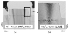
- FIG. 1 It is a figure which shows the process flow of the manufacturing method of the semiconductor device of this invention, and the evaluation method of a semiconductor device. It is the TEM photograph (a) of the cross section of the Fin structure part immediately after ion implantation, and the schematic diagram (b) which shows the direction of ion implantation. It is a schematic diagram which shows the line and space pattern (Fin structure part) of an Example, and the relationship of the direction of a notch. TEM photograph of the cross section of the Fin structure portion of Example 1 where the recovery heat treatment temperature is 600 ° C., the angle between the direction in which the Fin structure extends and the ⁇ 110 ⁇ direction of the silicon substrate is 45 °, and the recovery heat treatment time is 60 minutes ((a )).
- (B) is a partially enlarged photograph of (a).
- (B) is a partially enlarged photograph of (a).
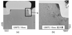
- a TEM photograph of a cross section of the Fin structure portion of Example 2 where the recovery heat treatment temperature is 1200 ° C., the angle between the extending direction of the Fin structure portion and the ⁇ 110 ⁇ direction of the silicon substrate is 45 °, and the recovery heat treatment time is 10 seconds ((a )).
- (B) is a partially enlarged photograph of (a).
- FIG. 1 It is a schematic diagram which shows the relationship between the line and space pattern (Fin structure part) in a comparative example, and the direction of a notch.
- the recovery heat treatment temperature is 600 ° C.
- the direction in which the Fin structure extends and the ⁇ 110 ⁇ direction of the silicon substrate are the same direction
- the recovery heat treatment time is 10 min ((a)), 30 min ((b)), 60 min ((c ))
- (D) is a partially enlarged photograph of (c).
- the inventors of the present invention have formed ion implantation defects such as twins remaining at the end of the Fin structure portion in the process of recovery heat treatment, which is caused by the difference in the recovery rate of crystallinity in the Fin structure portion. It was estimated that.
- a FinFET having a Fin structure is formed in a parallel direction or a vertical direction with respect to the ⁇ 110 ⁇ direction in which a notch is formed in a (100) wafer.
- This is related to the interface order density when the MOS (Metal Oxide Semiconductor) structure is used, and the (111) plane has a higher interface state and lowers the channel mobility. For this reason, there has been a history of adopting (100) wafers so far in MOS devices.
- the difference in the recrystallization speed of the Fin structure portion can be obtained.
- the inventors have found that ion implantation defects can be prevented from being reduced, and the present invention has been completed.
- a method for manufacturing a semiconductor device according to the present invention will be described with reference to FIGS.
- a silicon substrate is prepared, a photolithography process is performed, and then a dry etching process is performed to form a convex columnar structure (Fin structure portion) on the silicon substrate.
- the Fin structure portion is formed so that the ⁇ 110 ⁇ direction of the silicon substrate is different from the direction in which the Fin structure portion extends (step (a) in FIG. 1).
- the ⁇ 110 ⁇ direction means the direction of a plane group equivalent to the (110) plane.
- the Fin structure portion it is preferable to form the Fin structure portion so that an angle formed between the direction in which the Fin structure portion extends and the ⁇ 110 ⁇ direction of the silicon substrate is 1 ° or more and 89 ° or less. If the Fin structure portion is formed to have such an angle, it is possible to more reliably prevent defects from remaining inside the Fin structure portion. In addition, you may have another process before the process of forming Fin structure part.
- ions are implanted into this columnar structure. Since dopants need to be implanted not only into the vertical (vertical) direction as in conventional ion implantation but also into the sidewalls of the columnar structure, Ions are also implanted into the left and right side walls of the columnar structure from an inclined angle, and dopant is implanted into the entire columnar structure (step (b) in FIG. 1). At this time, the angle to be tilted with respect to the vertical is not particularly limited, but may be 45 °, for example. In addition, although ion species and implantation energy to be implanted are not particularly limited, for example, As can be implanted at 400 keV from right and left and right.
- FIG. 2A is a TEM (Transmission Electron Microscope) photograph of the cross section of the columnar structure, and the direction of ion implantation is indicated by a broken line.
- a dark black portion with contrast is a portion made amorphous by As implantation.
- FIG. 2B is a schematic diagram showing a columnar pattern (line and space (L / S) pattern; a pattern in which lines and spaces are alternately formed) formed on a silicon substrate and the direction of ion implantation.
- vertical ion implantation is omitted in FIG.
- a notch 11 is formed in the silicon substrate 10.
- a recovery heat treatment that serves as both defect recovery and activation is performed (step (c) in FIG. 1).
- annealing for a few milliseconds such as FLA (flash lamp annealing) or annealing for a few seconds such as RTA (rapid heating / rapid cooling heat treatment) is generally performed. Even when such a heat treatment is performed, defects generated by ion implantation remain in the columnar structure including the upper end portion of the columnar structure.
- the present inventors have found that if the columnar structure formation direction is changed from the ⁇ 110 ⁇ direction of the silicon substrate, defects at the tip of the columnar structure disappear.
- the silicon in the columnar structure becomes amorphous, and recrystallization occurs in the recovery heat treatment after the ion implantation.
- the single crystal portion that is the seed of recrystallization is the lower part of the columnar structure.
- recrystallization by recovery heat treatment proceeds from the single crystal portion under the columnar structure.
- the recrystallization speed is different inside the columnar structure (Non-Patent Document 2). Therefore, when the crystal grows in the ⁇ 111> axis direction by the recovery heat treatment, ion implantation defects tend to remain.
- the recrystallization rate inside the columnar structure portion is obtained unless crystal growth is performed in the ⁇ 111> axis direction. The difference between the two becomes small, and residual ion implantation defects can be prevented.
- a convex Fin structure is formed on the silicon substrate 10 (step (a) in FIG. 1), and ion implantation is performed from three directions, vertical and left and right (step (b) in FIG. 1). Subsequently, a recovery heat treatment that combines defect recovery and activation is performed (step (c) in FIG. 1). At this time, samples with different recovery heat treatment times are produced.
- the time for the recovery heat treatment depends on the heat treatment method, but when a batch-type heat treatment furnace capable of treating a large number of sheets at a time using a resistance heating method is used, it can be set to, for example, 3 minutes to 3 hours. Moreover, when RTA is used, it can be set to 1 second to 30 seconds, for example.
- step (d) in FIG. 1 by observing a cross section in a direction perpendicular to the direction in which the Fin structure portion of the manufactured sample extends (step (d) in FIG. 1), by ion implantation in the process of recrystallization of amorphous silicon. Defect evaluation can be performed.
- the heat treatment temperature is preferably performed in a temperature range of 550 ° C. or more and 650 ° C. or less. In this way, the rate of single crystal crystallization of amorphous silicon is suppressed, that is, annealing is performed at a low temperature, and recrystallization proceeds slowly over time, so the defect recovery behavior should be investigated more accurately. Is possible.
- the heat treatment temperature is preferably within a temperature range of 800 ° C. or higher and 1200 ° C. or lower. If the recovery heat treatment is performed in the RTA heat treatment furnace in such a temperature range, the recovery heat treatment can be performed in a short time of several tens of seconds or less, so that the behavior of defects in the Fin structure portion can be evaluated easily and in a short time.
- Example 1 Using a silicon substrate having a diameter of 200 mm doped with boron having a resistivity of 10 ⁇ ⁇ cm as a material, a photoresist was first applied to the substrate, and a photolithography process was performed. Then, the L / S pattern direction of this silicon substrate was prepared by tilting it by 1 ° and 45 ° from the normal ⁇ 110 ⁇ direction.
- 3A and 3B are schematic views showing that the direction of the L / S pattern is inclined by 1 ° and 45 ° from the ⁇ 110 ⁇ direction. In FIG. 3B, since the L / S pattern is formed by tilting the notch formed in the ⁇ 110 ⁇ direction by 45 °, the Fin structure portion is tilted by 45 ° with respect to the ⁇ 110 ⁇ direction.
- a negative resist was selected as the photoresist, and a 1.2 ⁇ m L / S pattern was formed on the silicon substrate (wafer) surface.
- This resist-coated wafer was etched by dry etching, and after removing the resist with a sulfuric acid hydrogen peroxide mixed solution, RCA cleaning was performed.
- the dry etching conditions at this time were an output condition of HBr and Cl 2 of 1: 1, a pressure of 1200 mmTorr, and 300 W.
- An As was driven into the wafer on which these Fin structure portions were formed at an acceleration voltage (acceleration energy) of 450 keV and a dose amount of 1 ⁇ 10 15 atoms / cm 2 from three directions, right above and left and right of the L / S pattern.
- FIGS. 4 shows the case where the angle between the ⁇ 110 ⁇ direction of the silicon substrate and the direction in which the Fin structure portion extends is 45 °, and FIG. 5 shows the case of 1 °. In either case, no defect remained at the tip of the Fin structure.
- Example 2 In the same manner as in Example 1, a photolithography process was performed using a silicon substrate having a diameter of 200 mm doped with boron having a resistivity of 10 ⁇ ⁇ cm.
- the notch position of this silicon substrate is the normal ⁇ 110 ⁇ direction, but the notch position was inclined by 1 ° and 45 ° from the original position during the photolithography process.
- FIG. 3B is a schematic diagram showing the relationship among the silicon substrate 10, the notch 11, and the L / S pattern when the fin structure (L / S pattern) is formed by tilting the notch position by 45 °.
- a negative resist was selected as the photoresist, and a 1.2 ⁇ mL / S pattern was formed on the wafer surface.
- This resist-coated wafer was etched by dry etching under the same conditions as in Example 1, and after removing the resist with a sulfuric acid hydrogen peroxide mixture, RCA cleaning was performed.
- These wafers were implanted with As at an acceleration voltage (acceleration energy) of 450 keV, a dose of 1 ⁇ 10 15 atoms / cm 2 , and As from three directions, right above the L / S pattern and left and right.
- the wafer which produced the Fin structure was annealed, and the recovery condition was observed by cross-sectional TEM.
- RTA was used for annealing, and the annealing temperature was set to 1200 ° C. in which defects are likely to remain when the amorphous is recrystallized.
- Atmosphere annealing was N 2.
- the annealing time was set to 10 seconds as a sufficient time for the amorphous silicon in the Fin structure portion to be single-crystallized.
- a TEM photograph of the result is shown in FIG.
- FIG. 6 is a TEM photograph when the notch position is tilted by 45 °. Also in this case, no defect was introduced at the tip of the Fin structure portion.
- the dry etching conditions at this time were as follows: HBr and Cl 2 were 1: 1, and the output conditions were a pressure of 1200 mmTorr and 300 W. These wafers were bombarded with As at an acceleration voltage (acceleration energy) of 450 keV and a dose of 1 ⁇ 10 15 atoms / cm 2 from three directions, right above the L / S pattern and left and right.
- acceleration voltage acceleration energy
- the wafer which produced the Fin structure part was annealed, and the recovery
- the annealing temperature was set at two conditions of 600 ° C. using a batch heat treatment furnace considered to have a very slow recrystallization rate of amorphous silicon and 1200 ° C. using RTA.
- the annealing atmosphere was N 2 for all.
- FIG. 8 shows a TEM photograph of the progress of recrystallization when annealing is performed at a recovery heat treatment temperature of 600 ° C. for different times. It can be seen that annealing at 600 ° C. for 10 minutes does not completely recrystallize the amorphous silicon in the Fin structure portion, and an amorphous portion (EOR (End-of-Range) defect) remains (FIG. 8A). reference). In the annealing at 600 ° C. for 30 minutes, a part of the amorphous portion remains at the tip portion of the Fin structure portion (see FIG. 8B). In the annealing at 600 ° C.
- the Fin structure portion is single-crystallized and no amorphous portion remains, but it can be seen that defects remain at the tip of the Fin structure portion (see FIG. 8C). Furthermore, when the TEM sample was thinned and observed at a high magnification, twins were observed at the tip of the Fin structure (see FIG. 8D). It is thought that twins were formed due to the difference in growth direction depending on the plane orientation.
- FIG. 9 shows the result of annealing for 10 seconds with a recovery heat treatment temperature of 1200 ° C. by RTA.
- a recovery heat treatment temperature of 1200 ° C. by RTA.
- the semiconductor device evaluation method of the present invention could easily evaluate defects due to ion implantation in the Fin structure portion and recrystallization of amorphous silicon without using a miniaturized state-of-the-art process.
- the present invention is not limited to the above embodiment.
- the above-described embodiment is an exemplification, and the present invention has substantially the same configuration as the technical idea described in the claims of the present invention, and any device that exhibits the same function and effect is the present invention. It is included in the technical scope of the invention.
Landscapes
- Insulated Gate Type Field-Effect Transistor (AREA)
- Testing Or Measuring Of Semiconductors Or The Like (AREA)
- Recrystallisation Techniques (AREA)
Abstract
本発明は、半導体シリコン基板上に、上に凸形状を有するFin構造部を形成し、Fin構造部にイオン注入を行った後、半導体シリコン基板に回復熱処理を行い、Fin構造部のシリコンを再結晶化する工程を有する半導体装置の製造方法であって、Fin構造部は少なくとも一方向に延在し、Fin構造部が延在する方向と半導体シリコン基板の{110}方向とが異なる方向となるようにFin構造部を形成することを特徴とする半導体装置の製造方法を提供する。これにより、半導体シリコン基板上にFin構造部を形成し、そのFin構造部にイオン注入し、半導体シリコン基板に回復熱処理を行った後に、Fin構造部にイオン注入による欠陥が残留しない半導体装置の製造方法が提供される。
Description
本発明は半導体装置の製造方法及び半導体装置の評価方法に関するものであり、より詳しくは半導体シリコン基板上にFin構造を形成する工程を有する半導体装置の製造方法及び半導体装置の評価方法に関する。
イオン注入技術は各種トランジスタをはじめとする半導体部品の製造において非常に重要な手法である。しかし、ドーパントとなる注入元素をイオン化して加速し、シリコンに注入する手法であるため、加速されたイオンによるシリコンへのダメージが発生する。このダメージ回避のために種々の手法が検討されているが、基本はダメージを受けたシリコンの結合(例えばアモルファス化したシリコン)を再構成し単結晶化するのに十分な高温で熱処理して回復させる手法である。
シリコン基板に酸化膜を形成してリソグラフィー工程及びエッチング工程により窓開けを行い、ここにイオン注入にて拡散層を形成する工程で作製される従来の平面構造トランジスタでは、ダメージの回復、すなわち、イオン注入層の再結晶化が埋め込み底部と側壁の両方向から起こる。
一方、微細な先端デバイスで採用されているFin構造では、イオン注入後の再結晶化がFin底部からのみ進むため、双晶などの欠陥が入ることがある(非特許文献1)。Fin構造では従来の埋め込み構造のイオン注入領域に比べて、イオン注入される領域が非常に小さいこと、上に凸形状の柱状構造に均一にイオン注入するために、従来の埋め込み構造のように、ウェーハ垂直方向からだけでなく、斜め方向からも注入を行うなどの特徴がある。さらに、微細化構造で採用されることから、イオン注入ダメージの回復アニールは非常に短時間となる傾向がある。これらのことから示唆されるように、FinFET(FET;電界効果トランジスタ)の柱状構造ではイオン注入後のダメージ・欠陥回復が不十分になる可能性がある。
Ext. Abs. the 13th International Workshop on Junction Technology,2013,p.22.
M.Tamura and M.Horiuchi,"Lattice Defects in High-dose As Implantation into Localized Si Area",Jpn.J.Appl.Phys.,27,p.2209-2217,1988.
本発明は、上記問題点に鑑みてなされたものであって、半導体シリコン基板上にFin構造部を形成し、そのFin構造部にイオン注入し、半導体シリコン基板に回復熱処理を行った後に、Fin構造部にイオン注入による欠陥が残留しない半導体装置の製造方法を提供することを目的とする。また、本発明はFin構造部のイオン注入による欠陥の評価を簡便に行うことができる半導体装置の評価方法を提供することを目的とする。
上記目的を達成するために、本発明は、半導体シリコン基板上に、上に凸形状を有するFin構造部を形成し、該Fin構造部にイオン注入を行った後、前記半導体シリコン基板に回復熱処理を行い、前記Fin構造部のシリコンを再結晶化する工程を有する半導体装置の製造方法であって、
前記Fin構造部は少なくとも一方向に延在し、該Fin構造部が延在する方向と前記半導体シリコン基板の{110}方向とが異なる方向となるように前記Fin構造部を形成することを特徴とする半導体装置の製造方法を提供する。
前記Fin構造部は少なくとも一方向に延在し、該Fin構造部が延在する方向と前記半導体シリコン基板の{110}方向とが異なる方向となるように前記Fin構造部を形成することを特徴とする半導体装置の製造方法を提供する。
このように、Fin構造部が延在する方向と半導体シリコン基板の{110}方向とが異なる方向となるようにFin構造部を形成することにより、回復熱処理後にFin構造部内にイオン注入による欠陥が残留するのを抑制することができる。
このとき、前記Fin構造部が延在する方向と前記半導体シリコン基板の{110}方向とのなす角度が1°以上となるように前記Fin構造部を形成することが好ましい。
このような角度となるようにFin構造部を形成すれば、Fin構造部の内部に欠陥が残留することをより確実に防ぐことができる。
このような角度となるようにFin構造部を形成すれば、Fin構造部の内部に欠陥が残留することをより確実に防ぐことができる。
さらに、上記目的を達成するために、本発明では、半導体シリコン基板上に、上に凸形状を有するFin構造部を形成し、該Fin構造部にイオン注入を行った後、前記半導体シリコン基板に回復熱処理を行い、前記Fin構造部のシリコンを再結晶化して、前記Fin構造部のイオン注入による欠陥を評価する方法であって、
前記Fin構造部は少なくとも一方向に延在し、該Fin構造部が延在する方向と前記半導体シリコン基板の{110}方向とが異なる方向となるように前記Fin構造部を形成し、
前記回復熱処理を時間を変えて実施し、前記Fin構造部の前記延在する方向に垂直方向の断面をTEMで観察することにより、前記再結晶化の進行過程でのイオン注入による欠陥の評価を行うことを特徴とする半導体装置の評価方法を提供する。
前記Fin構造部は少なくとも一方向に延在し、該Fin構造部が延在する方向と前記半導体シリコン基板の{110}方向とが異なる方向となるように前記Fin構造部を形成し、
前記回復熱処理を時間を変えて実施し、前記Fin構造部の前記延在する方向に垂直方向の断面をTEMで観察することにより、前記再結晶化の進行過程でのイオン注入による欠陥の評価を行うことを特徴とする半導体装置の評価方法を提供する。
このような半導体装置の評価方法であれば、微細化した最先端プロセスを用いなくともFin構造部の欠陥の挙動を簡便に評価することができる。
このとき、前記回復熱処理を抵抗加熱式のバッチ式熱処理炉を用いた場合は熱処理温度を550℃以上650℃以下の温度範囲で行うことが好ましい。
このような温度範囲の抵抗加熱式のバッチ式熱処理炉による回復熱処理であれば、再結晶化する速度が極めて遅いので、結晶化の進行過程での欠陥の評価を正確かつ詳細に行うことができる。
このような温度範囲の抵抗加熱式のバッチ式熱処理炉による回復熱処理であれば、再結晶化する速度が極めて遅いので、結晶化の進行過程での欠陥の評価を正確かつ詳細に行うことができる。
このとき、前記回復熱処理をRTA熱処理炉を用いた場合は熱処理温度を800℃以上1200℃以下の温度範囲で行うことが好ましい。
このような温度範囲のRTA熱処理炉による回復熱処理であれば、回復熱処理を数十秒以下の短い時間で行えるので、Fin構造部の欠陥の挙動を簡便かつ短時間で評価することができる。
このような温度範囲のRTA熱処理炉による回復熱処理であれば、回復熱処理を数十秒以下の短い時間で行えるので、Fin構造部の欠陥の挙動を簡便かつ短時間で評価することができる。
以上のように、本発明の半導体装置の製造方法によれば、先端デバイスで採用されるFin構造において、イオン注入後の残留ダメージによる欠陥発生を防ぐことが可能になり、Fin構造を使用した先端デバイスを高品質で製造することができる。また、本発明の半導体装置の評価方法によれば、微細化した最先端プロセスを用いなくともFin構造部のイオン注入による欠陥の挙動を簡便に評価することができる。
以下、本発明をより詳細に説明する。
本発明者らはFin構造部の端部に残留する双晶をはじめとしたイオン注入欠陥は回復熱処理の過程で形成されたもので、Fin構造部における結晶性の回復速度の違いが原因になっていると推定した。
本発明者らはFin構造部の端部に残留する双晶をはじめとしたイオン注入欠陥は回復熱処理の過程で形成されたもので、Fin構造部における結晶性の回復速度の違いが原因になっていると推定した。
一般にFin構造を有するFinFETは、(100)ウェーハでノッチが形成されている{110}方向を基準として平行方向または垂直方向に形成されている。これはMOS(Metal Oxide Semiconductor)構造としたときの界面順位密度と関係があり、(111)面は界面準位が高くなり、チャンネル移動度が低下するためである。このため、MOSデバイスではこれまで(100)ウェーハを採用してきた経緯がある。
この場合、回復熱処理におけるFin構造部の再結晶化は<111>軸方向に成長する。この<111>軸方向の結晶性の回復は(111)面全体の結晶性が回復してから次の(111)面の結晶性が回復するファセット成長機構となる。このとき、Fin構造部の温度分布が不均一な熱環境では(111)面全体の結晶性の回復が終了しない状態で次の(111)面の結晶性の回復が開始してしまい、結晶性が完全に回復しない状態で結晶成長(結晶性の回復)が進んでしまう。その結果、Fin構造部にイオン注入欠陥が残留しやすくなると推定した。
そして、Fin構造部が<111>軸方向に結晶成長をしないように、Fin構造部が延在する方向を{110}方向からわずかにずらせば、Fin構造部の再結晶化の速度の違いが小さくなり、イオン注入欠陥の残留を防止することができることを本発明者らは見出し、本発明を完成させた。
以下、本発明について、実施態様の一例として、図を参照しながら詳細に説明するが、本発明はこれに限定されるものではない。
最初に、本発明の半導体装置の製造方法について、図1及び図2を参照して説明する。
まず、シリコン基板を用意し、フォトリソグラフィー工程を行った後にドライエッチング工程を行い、シリコン基板上に上に凸の柱状の構造(Fin構造部)を形成する。このとき、シリコン基板の{110}方向とFin構造部が延在する方向が異なる方向となるように、Fin構造部を形成する(図1の(a)工程)。ここで、{110}方向とは(110)面と等価な面群の方向を意味している。
また、Fin構造部が延在する方向とシリコン基板の{110}方向とのなす角度が1°以上、89°以下となるようにFin構造部を形成することが好ましい。このような角度となるようにFin構造部を形成すれば、Fin構造部の内部に欠陥が残留することをより確実に防ぐことができる。
尚、Fin構造部を形成する工程の前に他の工程を有していてもよい。
まず、シリコン基板を用意し、フォトリソグラフィー工程を行った後にドライエッチング工程を行い、シリコン基板上に上に凸の柱状の構造(Fin構造部)を形成する。このとき、シリコン基板の{110}方向とFin構造部が延在する方向が異なる方向となるように、Fin構造部を形成する(図1の(a)工程)。ここで、{110}方向とは(110)面と等価な面群の方向を意味している。
また、Fin構造部が延在する方向とシリコン基板の{110}方向とのなす角度が1°以上、89°以下となるようにFin構造部を形成することが好ましい。このような角度となるようにFin構造部を形成すれば、Fin構造部の内部に欠陥が残留することをより確実に防ぐことができる。
尚、Fin構造部を形成する工程の前に他の工程を有していてもよい。
次に、この柱状構造にイオン注入を行うが、従来のイオン注入のように直上(垂直)方向からだけではなく、柱状構造の側壁へもドーパントを注入する必要があることから、垂直に対して傾けた角度から柱状構造の左右の側壁にもイオンを打ち込み、柱状構造全体にドーパントを注入する(図1の(b)工程)。このとき、垂直に対して傾ける角度は特に限定されないが、例えば45°とすることができる。また、注入するイオン種や注入エネルギーは特に限定されないが、例えばAsを400keVで直上と左右の三方向から注入することができる。
この傾けた角度からのイオン注入を図2に模式的に示した。図2(a)は柱状構造の断面のTEM(Transmission Electron Microscope)写真であり、イオン注入の方向を破線で示している。図2(a)において、コントラストのついた濃い黒の部分が、As注入によりアモルファス化した部分である。図2(b)はシリコン基板に形成された柱状パターン(ラインアンドスペース(L/S)パターン;ラインとスペースが交互にあるパターン)とイオン注入の方向を示す模式図である。但し、垂直方向のイオン注入は図2(b)では省略してある。シリコン基板10にはノッチ11が形成されている。
その後、欠陥回復と活性化を兼ねた回復熱処理(アニール)を行う(図1の(c)工程)。通常の先端デバイスの製造工程では、一般にFLA(フラッシュランプアニール)のような数ミリ秒という短時間アニールや、RTA(急速加熱・急速冷却熱処理)という数秒のアニールが行われる。このような熱処理を施しても、柱状構造の上側先端部をはじめとする柱状構造内には、イオン注入にて生じた欠陥が残留する。それに対し、柱状構造の形成方向をシリコン基板の{110}方向から変更すると、柱状構造先端部の欠陥の残留がなくなることを本発明者らは見出した。
イオン注入後は、柱状構造部のシリコンはアモルファスになり、これの再結晶化がイオン注入後の回復熱処理で起こるが、柱状構造では再結晶化の種となる単結晶部が柱状構造部の下部にしかなく、回復熱処理による再結晶化は柱状構造下部の単結晶部分から進んでいく。このとき、柱状構造部の内部では再結晶化の速度が異なっていると考えられる(非特許文献2)。そのため、回復熱処理で結晶が<111>軸方向に成長するとイオン注入欠陥が残留しやすくなる。
これに対し、シリコン基板の{110}方向とFin構造部が延在する方向が異なる方向とすることにより、<111>軸方向に結晶成長させなければ、柱状構造部の内部の再結晶化速度の違いが小さくなり、イオン注入欠陥の残留を防止することができる。
次に、本発明の半導体装置の評価方法について、図1及び図2を参照して説明する。
シリコン基板10上に凸形状のFin構造部を形成し(図1の工程(a))、垂直及び左右の三方向からイオン注入を行う(図1の工程(b))。続いて、欠陥回復と活性化を兼ねた回復熱処理を行うが(図1の(c)工程)、このとき回復熱処理の時間を変えたサンプルを作製する。回復熱処理の時間は熱処理の方式に依存するが、抵抗加熱式で多数枚を一度に処理可能なバッチ式の熱処理炉を使用した場合には、例えば3分から3時間とすることができる。また、RTAを用いた場合には、例えば1秒から30秒とすることができる。
シリコン基板10上に凸形状のFin構造部を形成し(図1の工程(a))、垂直及び左右の三方向からイオン注入を行う(図1の工程(b))。続いて、欠陥回復と活性化を兼ねた回復熱処理を行うが(図1の(c)工程)、このとき回復熱処理の時間を変えたサンプルを作製する。回復熱処理の時間は熱処理の方式に依存するが、抵抗加熱式で多数枚を一度に処理可能なバッチ式の熱処理炉を使用した場合には、例えば3分から3時間とすることができる。また、RTAを用いた場合には、例えば1秒から30秒とすることができる。
そして、作製したサンプルのFin構造部が延在する方向に垂直方向の断面をTEMにより観察することにより(図1の(d)工程)、アモルファスシリコンの再結晶化の進行過程でのイオン注入による欠陥の評価を行うことができる。
ここで、回復熱処理を抵抗加熱式のバッチ式熱処理炉を用いた場合は熱処理温度を550℃以上650℃以下の温度範囲で行うことが好ましい。このように、アモルファスシリコンが単結晶化する速度を抑える、すなわち、低温でのアニールを行うことで、再結晶化が時間をかけてゆっくり進行するため、欠陥回復挙動をより正確に調査検討することが可能になる。
また、回復熱処理をRTA熱処理炉を用いた場合は熱処理温度を800℃以上1200℃以下の温度範囲で行うことが好ましい。このような温度範囲のRTA熱処理炉による回復熱処理であれば、回復熱処理を数十秒以下の短い時間で行えるので、Fin構造部の欠陥の挙動を簡便かつ短時間で評価することができる。
以下、実施例及び比較例を示して本発明をより具体的に説明するが、本発明はこれらに限定されるものではない。
(実施例1)
抵抗率10Ω・cmのボロンをドープした直径200mmシリコン基板を材料として、まずこの基板にフォトレジストを塗布し、フォトリソグラフィー工程を実施した。そして、このシリコン基板のL/Sパターンの方向を通常の{110}方向から1°および45°傾けたものを準備した。図3(a)及び(b)はL/Sパターンの方向を{110}方向から1°及び45°傾けたことを示す模式図である。図3(b)では{110}方向に形成したノッチを45°傾けてL/Sパターンを形成しているので、Fin構造部は{110}方向に対して45°傾いている。
抵抗率10Ω・cmのボロンをドープした直径200mmシリコン基板を材料として、まずこの基板にフォトレジストを塗布し、フォトリソグラフィー工程を実施した。そして、このシリコン基板のL/Sパターンの方向を通常の{110}方向から1°および45°傾けたものを準備した。図3(a)及び(b)はL/Sパターンの方向を{110}方向から1°及び45°傾けたことを示す模式図である。図3(b)では{110}方向に形成したノッチを45°傾けてL/Sパターンを形成しているので、Fin構造部は{110}方向に対して45°傾いている。
そして、フォトレジストとしてネガレジストを選択し、1.2μmのL/Sパターンをシリコン基板(ウェーハ)面内に形成した。このレジスト付きウェーハをドライエッチングにてエッチングし、硫酸過酸化水素混合液にてレジストを除去後、RCA洗浄を実施した。このときのドライエッチング条件は、HBrとCl2を1:1として、圧力を1200mmTorr、300Wの出力条件とした。これらのFin構造部を形成したウェーハに加速電圧(加速エネルギー)450keV、ドーズ量を1×1015atoms/cm2としてAsをL/Sパターンの直上と左右の3方向から打ちこんだ。
このようにしてFin構造部を作製したウェーハをアニールし、回復状況を断面TEMで観察した。アニールの雰囲気はN2とした。アニール温度はアモルファスが再結晶化する際に欠陥が残留しやすい600℃とし、時間はFin構造部のアモルファスシリコンが単結晶化するのに十分な時間として60分とした。その結果のTEM写真を図4及び図5に示す。図4は、シリコン基板の{110}方向とFin構造部が延在する方向のなす角度が、45°の場合であり、図5は1°の場合である。いずれの場合も、Fin構造部の先端には欠陥が残留していなかった。
(実施例2)
実施例1と同様に、抵抗率10Ω・cmのボロンをドープした直径200mmシリコン基板を材料として、フォトリソグラフィー工程を実施した。このシリコン基板のノッチ位置は通常の{110}方向であるが、フォトリソグラフィー工程時にノッチ位置を本来の位置から1°および45°傾けて実施した。図3(b)にノッチ位置を45°傾けてFin構造部(L/Sパターン)を形成した場合のシリコン基板10、ノッチ11、及びL/Sパターンの関係の模式図を示す。
実施例1と同様に、抵抗率10Ω・cmのボロンをドープした直径200mmシリコン基板を材料として、フォトリソグラフィー工程を実施した。このシリコン基板のノッチ位置は通常の{110}方向であるが、フォトリソグラフィー工程時にノッチ位置を本来の位置から1°および45°傾けて実施した。図3(b)にノッチ位置を45°傾けてFin構造部(L/Sパターン)を形成した場合のシリコン基板10、ノッチ11、及びL/Sパターンの関係の模式図を示す。
フォトレジストとしてネガレジストを選択し、1.2μmL/Sパターンをウェーハ面内へ形成した。このレジスト付きウェーハを、実施例1と同条件でドライエッチングにてエッチングし、硫酸過酸化水素混合液にてレジストを除去後、RCA洗浄を実施した。これらのウェーハに加速電圧(加速エネルギー)450keVで、ドーズ量を1×1015atoms/cm2としてAsをL/Sパターンの直上と左右の3方向から打ちこんだ。
このようにしてFin構造を作製したウェーハをアニールし、回復状況を断面TEMで観察した。アニールにはRTAを使用し、アニール温度はアモルファスが再結晶化する際に欠陥が残留しやすい1200℃とした。アニールの雰囲気はN2とした。アニール時間はFin構造部のアモルファスシリコンが単結晶化するのに十分な時間として10secとした。その結果のTEM写真を図6に示す。図6は、ノッチ位置を45°傾けた場合のTEM写真である。この場合も、Fin構造部の先端には欠陥が導入されていなかった。
(比較例1)
抵抗率10Ω・cmのボロンをドープした直径200mmのシリコン基板を材料として、これにフォトレジストを塗布し、フォトリソグラフィー工程を行った。このときのノッチ位置は{110}方向で、L/Sパターンは図7に示すように、そのまま{110}方向に形成した。フォトレジストはネガレジストを使用し、1.2μmL/Sパターンをウェーハ面内へ形成した。このレジスト付きウェーハをドライエッチングにてエッチングし、硫酸過酸化水素混合液にてレジストを除去後、RCA洗浄を実施した。このときのドライエッチング条件はHBrとCl2を1:1として、圧力1200mmTorr、300Wの出力条件とした。これらのウェーハに加速電圧(加速エネルギー)450keV、ドーズ量を1×1015atoms/cm2としてAsをL/Sパターンの直上と左右の3方向から打ちこんだ。
抵抗率10Ω・cmのボロンをドープした直径200mmのシリコン基板を材料として、これにフォトレジストを塗布し、フォトリソグラフィー工程を行った。このときのノッチ位置は{110}方向で、L/Sパターンは図7に示すように、そのまま{110}方向に形成した。フォトレジストはネガレジストを使用し、1.2μmL/Sパターンをウェーハ面内へ形成した。このレジスト付きウェーハをドライエッチングにてエッチングし、硫酸過酸化水素混合液にてレジストを除去後、RCA洗浄を実施した。このときのドライエッチング条件はHBrとCl2を1:1として、圧力1200mmTorr、300Wの出力条件とした。これらのウェーハに加速電圧(加速エネルギー)450keV、ドーズ量を1×1015atoms/cm2としてAsをL/Sパターンの直上と左右の3方向から打ちこんだ。
このようにしてFin構造部を作製したウェーハをアニールし回復状況を断面TEMで観察した。アニール温度はアモルファスシリコンが再結晶化する速度が極めて遅いと考えられるバッチ式熱処理炉による600℃と、RTAを使った1200℃の2つの条件とした。アニールの雰囲気はいずれもN2とした。
図8に回復熱処理温度600℃で時間を変えてアニールしたときの再結晶化の進行過程のTEM写真を示す。600℃、10分のアニールではFin構造部のアモルファスシリコンは完全に再結晶化せず、アモルファス部(EOR(End-of-Range)欠陥)が残留していることが分かる(図8(a)参照)。600℃、30分のアニールでは、Fin構造部の先端部に一部アモルファス部が残留している(図8(b)参照)。600℃、60分のアニールではFin構造部内は単結晶化しアモルファス部は残っていないが、Fin構造部の先端部に欠陥が残留していることが分かる(図8(c)参照)。更に、TEMサンプルを薄膜化し、高倍率で観察したところ、Fin構造部の先端部に双晶が確認された(図8(d)参照)。面方位による成長方向の違いで、双晶が生じたのではないかと考えられる。
次に、RTAにて回復熱処理温度を1200℃として、10秒のアニールを行った結果を図9に示す。高温になることで、Fin構造部の先端部の欠陥量は600℃の場合より少なくなったが、このような高温であっても、イオン注入により導入された欠陥が残留することが分かった。
以上のように、Fin構造部が延在する方向と半導体シリコン基板の{110}方向とが異なる場合は、回復熱処理後のFin構造部にはイオン注入による欠陥は観察されなかった。これに対して、Fin構造部が延在する方向とシリコン基板の{110}方向とが同じ場合には、回復熱処理を十分実施してもFin構造部の先端部のイオン注入による欠陥をなくすことはできなかった。
また、本発明の半導体装置の評価方法により、微細化した最先端プロセスを用いなくとも、Fin構造部のイオン注入による欠陥やアモルファス化したシリコンの再結晶化を簡便に評価することができた。
なお、本発明は、上記実施形態に限定されるものではない。上記実施形態は、例示であり、本発明の特許請求の範囲に記載された技術的思想と実質的に同一な構成を有し、同様な作用効果を奏するものは、いかなるものであっても本発明の技術的範囲に包含される。
Claims (5)
- 半導体シリコン基板上に、上に凸形状を有するFin構造部を形成し、該Fin構造部にイオン注入を行った後、前記半導体シリコン基板に回復熱処理を行い、前記Fin構造部のシリコンを再結晶化する工程を有する半導体装置の製造方法であって、
前記Fin構造部は少なくとも一方向に延在し、該Fin構造部が延在する方向と前記半導体シリコン基板の{110}方向とが異なる方向となるように前記Fin構造部を形成することを特徴とする半導体装置の製造方法。 - 前記Fin構造部が延在する方向と前記半導体シリコン基板の{110}方向とのなす角度が1°以上となるように前記Fin構造部を形成することを特徴とする請求項1に記載の半導体装置の製造方法。
- 半導体シリコン基板上に、上に凸形状を有するFin構造部を形成し、該Fin構造部にイオン注入を行った後、前記半導体シリコン基板に回復熱処理を行い、前記Fin構造部のシリコンを再結晶化して、前記Fin構造部のイオン注入による欠陥を評価する方法であって、
前記Fin構造部は少なくとも一方向に延在し、該Fin構造部が延在する方向と前記半導体シリコン基板の{110}方向とが異なる方向となるように前記Fin構造部を形成し、
前記回復熱処理を時間を変えて実施し、前記Fin構造部の前記延在する方向に垂直方向の断面をTEMで観察することにより、前記再結晶化の進行過程でのイオン注入による欠陥の評価を行うことを特徴とする半導体装置の評価方法。 - 前記回復熱処理を抵抗加熱式のバッチ式熱処理炉を用いた場合は熱処理温度を550℃以上650℃以下の温度範囲で行うことを特徴とする請求項3に記載の半導体装置の評価方法。
- 前記回復熱処理をRTA熱処理炉を用いた場合は熱処理温度を800℃以上1200℃以下の温度範囲で行うことを特徴とする請求項3に記載の半導体装置の評価方法。
Applications Claiming Priority (2)
| Application Number | Priority Date | Filing Date | Title |
|---|---|---|---|
| JP2015-083169 | 2015-04-15 | ||
| JP2015083169A JP6323383B2 (ja) | 2015-04-15 | 2015-04-15 | 半導体装置の評価方法 |
Publications (1)
| Publication Number | Publication Date |
|---|---|
| WO2016166930A1 true WO2016166930A1 (ja) | 2016-10-20 |
Family
ID=57126745
Family Applications (1)
| Application Number | Title | Priority Date | Filing Date |
|---|---|---|---|
| PCT/JP2016/001236 Ceased WO2016166930A1 (ja) | 2015-04-15 | 2016-03-08 | 半導体装置の製造方法及び半導体装置の評価方法 |
Country Status (2)
| Country | Link |
|---|---|
| JP (1) | JP6323383B2 (ja) |
| WO (1) | WO2016166930A1 (ja) |
Cited By (1)
| Publication number | Priority date | Publication date | Assignee | Title |
|---|---|---|---|---|
| WO2018020961A1 (ja) * | 2016-07-26 | 2018-02-01 | 信越半導体株式会社 | 半導体装置の製造方法及び半導体装置の評価方法 |
Families Citing this family (1)
| Publication number | Priority date | Publication date | Assignee | Title |
|---|---|---|---|---|
| JP2021034408A (ja) * | 2019-08-15 | 2021-03-01 | 信越半導体株式会社 | シリコン基板の熱処理方法 |
Citations (5)
| Publication number | Priority date | Publication date | Assignee | Title |
|---|---|---|---|---|
| WO1997006564A1 (fr) * | 1995-08-07 | 1997-02-20 | Hitachi, Ltd. | Dispositif a semiconducteur et procede de fabrication |
| JP2005236305A (ja) * | 2004-02-20 | 2005-09-02 | Samsung Electronics Co Ltd | トリプルゲートトランジスタを有する半導体素子及びその製造方法 |
| JP2011249780A (ja) * | 2010-04-28 | 2011-12-08 | Semiconductor Energy Lab Co Ltd | 半導体基板の作製方法及び光電変換装置の作製方法 |
| JP2014063897A (ja) * | 2012-09-21 | 2014-04-10 | Toshiba Corp | 半導体装置の製造方法、アニール装置及びアニール方法 |
| US20150024565A1 (en) * | 2012-06-25 | 2015-01-22 | Shigenobu Maeda | Method of forming semiconductor device having embedded strain-inducing pattern |
-
2015
- 2015-04-15 JP JP2015083169A patent/JP6323383B2/ja active Active
-
2016
- 2016-03-08 WO PCT/JP2016/001236 patent/WO2016166930A1/ja not_active Ceased
Patent Citations (5)
| Publication number | Priority date | Publication date | Assignee | Title |
|---|---|---|---|---|
| WO1997006564A1 (fr) * | 1995-08-07 | 1997-02-20 | Hitachi, Ltd. | Dispositif a semiconducteur et procede de fabrication |
| JP2005236305A (ja) * | 2004-02-20 | 2005-09-02 | Samsung Electronics Co Ltd | トリプルゲートトランジスタを有する半導体素子及びその製造方法 |
| JP2011249780A (ja) * | 2010-04-28 | 2011-12-08 | Semiconductor Energy Lab Co Ltd | 半導体基板の作製方法及び光電変換装置の作製方法 |
| US20150024565A1 (en) * | 2012-06-25 | 2015-01-22 | Shigenobu Maeda | Method of forming semiconductor device having embedded strain-inducing pattern |
| JP2014063897A (ja) * | 2012-09-21 | 2014-04-10 | Toshiba Corp | 半導体装置の製造方法、アニール装置及びアニール方法 |
Cited By (2)
| Publication number | Priority date | Publication date | Assignee | Title |
|---|---|---|---|---|
| WO2018020961A1 (ja) * | 2016-07-26 | 2018-02-01 | 信越半導体株式会社 | 半導体装置の製造方法及び半導体装置の評価方法 |
| US10886129B2 (en) | 2016-07-26 | 2021-01-05 | Shin-Etsu Handotai Co., Ltd. | Method for manufacturing semiconductor device and method for evaluating semiconductor device |
Also Published As
| Publication number | Publication date |
|---|---|
| JP2016207682A (ja) | 2016-12-08 |
| JP6323383B2 (ja) | 2018-05-16 |
Similar Documents
| Publication | Publication Date | Title |
|---|---|---|
| CN100353497C (zh) | 半导体器件的制造方法 | |
| TWI475600B (zh) | 鰭型場效電晶體裝置及多重閘極電晶體裝置的形成方法 | |
| TWI763691B (zh) | 半導體元件與半導體元件的製造方法 | |
| TWI596649B (zh) | 在應變鬆弛緩衝層上方形成具應變之磊晶半導體材料的方法 | |
| JPH10500254A (ja) | 半導体基板中に埋め込まれた酸化物層を備えた低転位密度構造の製造プロセス | |
| US8343825B2 (en) | Reducing dislocation formation in semiconductor devices through targeted carbon implantation | |
| JP6323383B2 (ja) | 半導体装置の評価方法 | |
| KR102312816B1 (ko) | 반도체 장치의 제조방법 및 반도체 장치의 평가방법 | |
| CN103632925B (zh) | 半导体器件制造方法 | |
| US11424164B2 (en) | Enhanced etch resistance for insulator layers implanted with low energy ions | |
| US7122452B2 (en) | Method of manufacturing a semiconductor on a silicon on insulator (SOI) substrate using solid epitaxial regrowth (SPER) and semiconductor device made thereby | |
| JPH06216137A (ja) | 半導体装置およびその製造方法 | |
| CN112885716B (zh) | 半导体结构的形成方法 | |
| JPH0964355A (ja) | 半導体素子の製造方法 | |
| JPH04293241A (ja) | 半導体基板の製造方法 | |
| US8030183B2 (en) | Method for reducing crystal defect of SIMOX wafer and SIMOX wafer | |
| JP2011077066A (ja) | 半導体基板の製造方法 | |
| KR100992215B1 (ko) | 반도체소자의 트랜지스터 형성방법 | |
| KR101002045B1 (ko) | 반도체소자의 트랜지스터 형성방법 | |
| EP1577932A2 (en) | Method of manufacturing a semiconductor on a silicon on insulator (SOI) substrate using solid epitaxial regrowth (SPER) and semiconductor device made thereby | |
| CN104835786B (zh) | 一种制作半导体器件的方法 | |
| CN103972065A (zh) | SiGe层的形成方法 | |
| JPH0529243A (ja) | 半導体装置の製造方法 | |
| JP2002280320A (ja) | 半導体装置の製造方法 | |
| JP2010118382A (ja) | Simoxウェーハの結晶欠陥の低減方法 |
Legal Events
| Date | Code | Title | Description |
|---|---|---|---|
| 121 | Ep: the epo has been informed by wipo that ep was designated in this application |
Ref document number: 16779729 Country of ref document: EP Kind code of ref document: A1 |
|
| NENP | Non-entry into the national phase |
Ref country code: DE |
|
| 122 | Ep: pct application non-entry in european phase |
Ref document number: 16779729 Country of ref document: EP Kind code of ref document: A1 |